Embed Size (px)
Citation preview

Lecture 2: Field Programmable Gate Arrays I September 5, 2013
ECE 636
Reconfigurable Computing
Lecture 2
Field Programmable Gate Arrays I

Lecture 2: Field Programmable Gate Arrays I September 5, 2013
Overview
• Anti-fuse and EEPROM-based devices
• Contemporary SRAM devices
- Wiring
- Embedded
• New trends
- Single-driver wiring
- Power optimization

Lecture 2: Field Programmable Gate Arrays I September 5, 2013
22V10 PAL° Combinational logic
elements (SoP)
° Sequential logicelements (D-FFs)
° Up to 10 outputs
° Up to 10 FFs
° Up to 22 inputs

Lecture 2: Field Programmable Gate Arrays I September 5, 2013
Antifuse Switch
Metal 3
Metal-to-Metal Antifuse
Metal 2
Via
Metal 1
Contact
Silicon
• Anti-fuses are one-time programmable.
- Pulse eliminates dielectric
- Only need to program once.

Lecture 2: Field Programmable Gate Arrays I September 5, 2013
Anti-Fuse FPGA
• Negligible programming overhead
• Low capacitance routing (fast)
• Security
• Tolerant of firm errors• Resistance of about 100
antifuse polysilicon ONO dielectric
n+ antifuse diffusion
2

Lecture 2: Field Programmable Gate Arrays I September 5, 2013
Interconnection Fabric
Logic Module
Horizontal Track
Vertical Track
Anti-fuse
Typical Actel Anti-fuse Interconnect

Lecture 2: Field Programmable Gate Arrays I September 5, 2013
° Very good for design security• No bitstream can be intercepted in the field (no bitstream
transfer, no external configuration device)
• Need a Scanning Electron Microscope (SEM) to try to know the antifuse states (an Actel AX2OOO antifuse FPGA contains 53 million antifuses with only 2-5% programmed in an average design)
Anti-fuse Security
©ACTEL
Courtesy: Burleson/Gogniat

Lecture 2: Field Programmable Gate Arrays I September 5, 2013
FLASH-Memory Switch
SEL 1 SEL 2
SWITCHPRG/SEN
WORD LINE

Lecture 2: Field Programmable Gate Arrays I September 5, 2013
Flash/EEPROM Trends
• Logic elements (LUTs and flip flops)
• Segmented routing
• Low logic to register ratio
• Future?
Altera Max II

Lecture 2: Field Programmable Gate Arrays I September 5, 2013
SRAM-based FPGA
• SRAM bits can be programmed many times
• Each programming bit takes up five transistors
• Larger device area reduces speed versus EPROM and antifuse.
Read or Write
Data
Q
Q
Programming Bit I1I2
P1
P2P3P4
Out
2-Input LUT

Lecture 2: Field Programmable Gate Arrays I September 5, 2013
Field Programmable Gate Array

Lecture 2: Field Programmable Gate Arrays I September 5, 2013
Design Tradeoffs
• Some logic clusters are large (e.g. Altera contains 8 LUT-FF pairs)
• Three important issues:
- Logic elements per cluster
- Cluster connectivity to interconnect – wires (FC) – connection flexibility
- Switchbox flexibility (Fs)
LogicCluster
IO connectionsswitchbox

Lecture 2: Field Programmable Gate Arrays I September 5, 2013
Issue 1: The Logic Cluster
• Question: How many BLE should there be per cluster?
Lecture 2: Field Programmable Gate Arrays I September 5, 2013
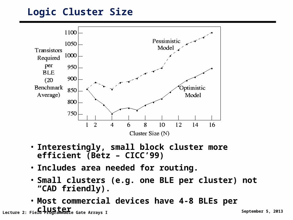
Logic Cluster Size
• Interestingly, small block cluster more efficient (Betz – CICC’99)
• Includes area needed for routing.
• Small clusters (e.g. one BLE per cluster) not “CAD friendly).
• Most commercial devices have 4-8 BLEs per cluster

Lecture 2: Field Programmable Gate Arrays I September 5, 2013
Number of Inputs per Cluster
• Lots of opportunities for input sharing in large clusters (Betz – CICC’99)
• Reducing inputs reduces the size of the device and makes it faster.
• Most FPGA devices (Xilinx, Lucent) have 4 BLE per cluster with more inputs than actually needed.

Lecture 2: Field Programmable Gate Arrays I September 5, 2013
Connection Box Flexibility
• Fc -> How many tracks does an input pin connect to?
• If logic cluster is small, FC is large FC = W
• If logic cluster is large, Fc can be less.
- Approximately 0.2W for Xilinx XC4000EX
LogicCluster
IO pin
Tracks
OutT0 T1 T2
T0T1T2
Out
FC = 3T0 T1 T2

Lecture 2: Field Programmable Gate Arrays I September 5, 2013
Switchbox Flexibility
• Switch box provides optimized interconnection area.
• Flexibility found to be not as important as FC
• Six transistors needed for FS= 3
0
1
0
1
0 1
0 1

Lecture 2: Field Programmable Gate Arrays I September 5, 2013
Switchbox Issues
Lecture 2: Field Programmable Gate Arrays I September 5, 2013
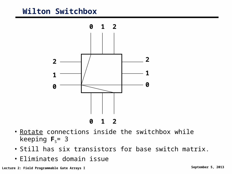
Wilton Switchbox
• Rotate connections inside the switchbox while keeping FS= 3
• Still has six transistors for base switch matrix.
• Eliminates domain issue
0 21
2
0
1
2
0
1
0 21

Lecture 2: Field Programmable Gate Arrays I September 5, 2013
Switchbox Issues

Lecture 2: Field Programmable Gate Arrays I September 5, 2013
Buffering
• FPGAs need to buffer to isolate large RC networks
• Architects must decide where to place buffers.
S S

Lecture 2: Field Programmable Gate Arrays I September 5, 2013
Segmentation
• Segmentation distribution: how many of each length?
• Longer length
- Better performance? - Reduced routability?
X Y
Length 4
Length 2
Length 1

Lecture 2: Field Programmable Gate Arrays I September 5, 2013
Modern CLB (V5): Slices
Source: Brad Hutchings, BYU
• More hierarchy in current devices
• Slices are complex. Multiple slices communicate with switch matrix
Lecture 2: Field Programmable Gate Arrays I September 5, 2013
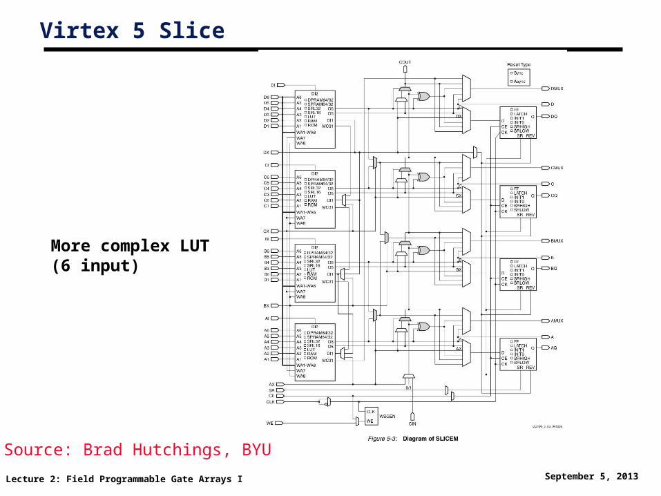
Virtex 5 Slice
Source: Brad Hutchings, BYU
More complex LUT(6 input)

Lecture 2: Field Programmable Gate Arrays I September 5, 2013
Implementing Memory on FPGAs
• For 4-input LUTs 16 bits of information available
• Can be chained together through programmable network.
• Decoder and multiplexer an issue.
• Flexibility is a key aspect.
Addr
A D
A D
16X1
16X1LUT1
LUT2
Lecture 2: Field Programmable Gate Arrays I September 5, 2013
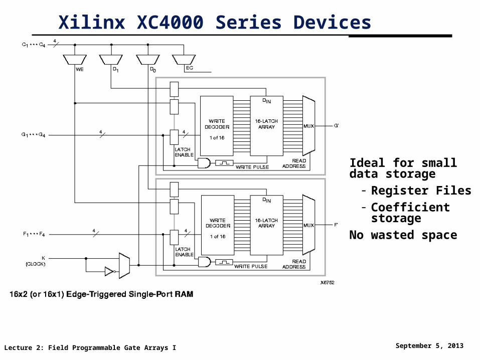
Xilinx XC4000 Series Devices
• Ideal for small data storage
- Register Files- Coefficient
storage• No wasted space

Lecture 2: Field Programmable Gate Arrays I September 5, 2013
Xilinx XC4000 Dual Port Mem
• Access data concurrently.
• Fine-grained access
• Synchronous access
Lecture 2: Field Programmable Gate Arrays I September 5, 2013
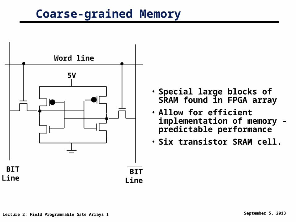
Coarse-grained Memory
• Special large blocks of SRAM found in FPGA array
• Allow for efficient implementation of memory – predictable performance
• Six transistor SRAM cell.
5V
Word line
BITLine
BITLine

Lecture 2: Field Programmable Gate Arrays I September 5, 2013
Xilinx Block Memory
• Each memory block is 4 CLBs high
• 4096 bit SRAMs.
• Can be implemented in differeent aspect ratios.
• Need to address performance.

Lecture 2: Field Programmable Gate Arrays I September 5, 2013
Stratix-4 Block Diagram
Courtesy: Brad Hutchings

Lecture 2: Field Programmable Gate Arrays I September 5, 2013
Stratix-4 ALM (LE)
Courtesy: Brad Hutchings

Lecture 2: Field Programmable Gate Arrays I September 5, 2013
Inside the EAB - Altera
• Embedded array highly optimized
• Address and data can be latched for fast performance.
• Scalable to even larger sizes.

Lecture 2: Field Programmable Gate Arrays I September 5, 2013
Inside the ESB• Embedded System Blocks can be configured as either memory or PLA.
• Multiple levels of hierarchy.
Lecture 2: Field Programmable Gate Arrays I September 5, 2013
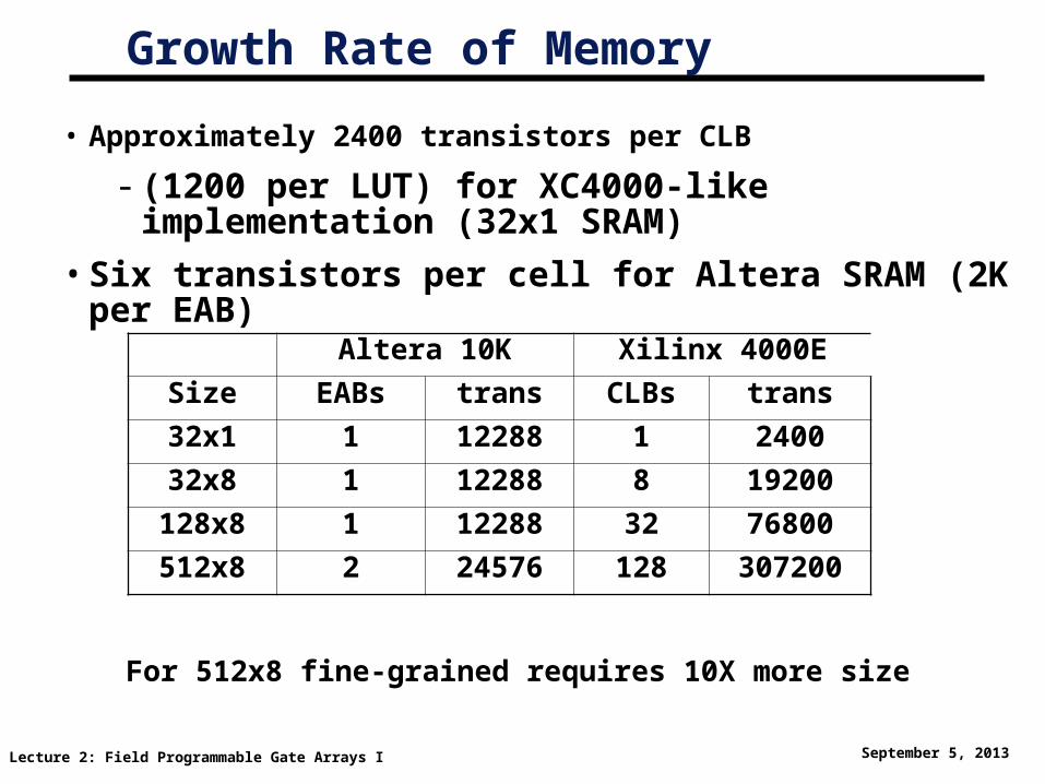
Growth Rate of Memory
• Approximately 2400 transistors per CLB
- (1200 per LUT) for XC4000-like implementation (32x1 SRAM)
• Six transistors per cell for Altera SRAM (2K per EAB)
Altera 10K Xilinx 4000E
Size EABs trans CLBs trans
32x1 1 12288 1 2400
32x8 1 12288 8 19200
128x8 1 12288 32 76800
512x8 2 24576 128 307200
For 512x8 fine-grained requires 10X more size
Lecture 2: Field Programmable Gate Arrays I September 5, 2013
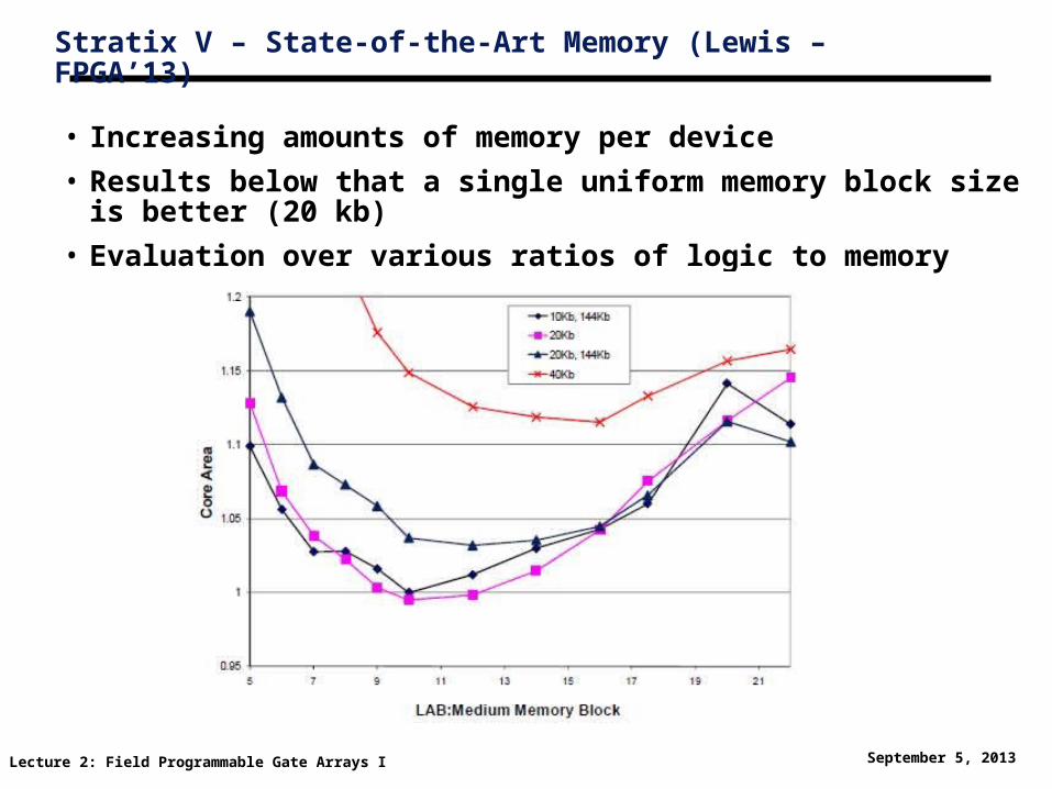
Stratix V – State-of-the-Art Memory (Lewis – FPGA’13)
• Increasing amounts of memory per device
• Results below that a single uniform memory block size is better (20 kb)
• Evaluation over various ratios of logic to memory
Lecture 2: Field Programmable Gate Arrays I September 5, 2013
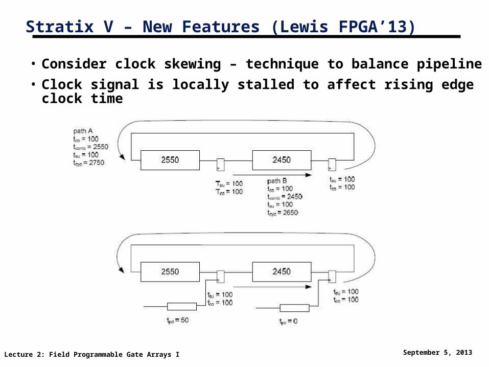
Stratix V – New Features (Lewis FPGA’13)
• Consider clock skewing – technique to balance pipeline
• Clock signal is locally stalled to affect rising edge clock time

Lecture 2: Field Programmable Gate Arrays I September 5, 2013
Summary
• Three basic types of FPGA devices
- Antifuse
- EEPROM
- SRAM
• Key issues for SRAM FPGA are logic cluster, connection box, and switch box.
• Latest advances examine performance and routability.
• Newer FPGAs require large amounts of RAM.
- Trends indicate uniform blocks
- Experimentation over many benchmarks is key


![Architecture of field-programmable gate arrays ...arantxa.ii.uam.es/~die/[Lectura FPGA Architecture] Architecture of... · Architecture of Field-Programmable Gate Arrays JONATHAN](https://img.pdfslide.net/doc/110x75/5f41b9382d13750b786f03bd/architecture-of-field-programmable-gate-arrays-dielectura-fpga-architecture.jpg)


![Field Programmable Gate Arrays [Fpga]](https://img.pdfslide.net/doc/110x75/544092dcb1af9f441d8b45c9/field-programmable-gate-arrays-fpga.jpg)