Embed Size (px)
Citation preview
Lecture 4: Signal Conditioning
Some of these slides are prepared by Dr. Chok Keawboonchuay, Assumption University.
1
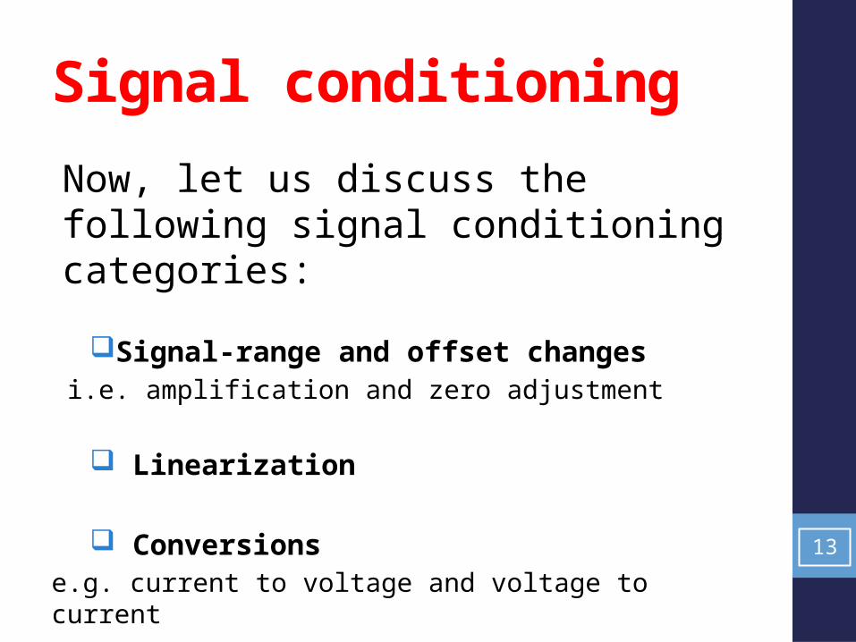
Signal Conditioning
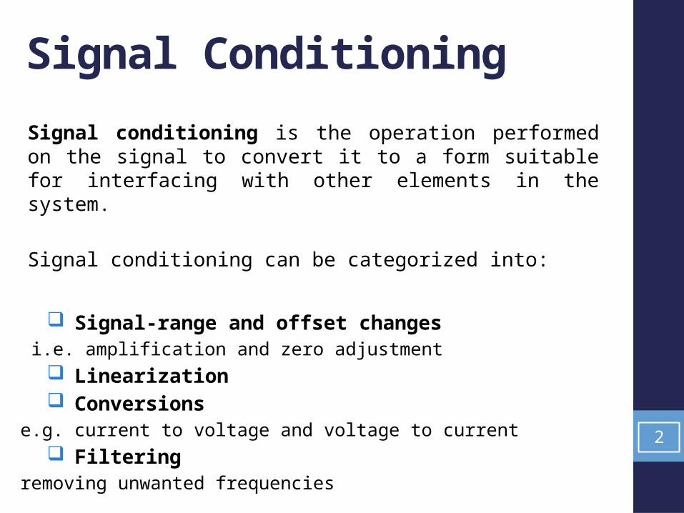
Signal conditioning is the operation performed on the signal to convert it to a form suitable for interfacing with other elements in the system.
Signal conditioning can be categorized into:
Signal-range and offset changesi.e. amplification and zero adjustment
Linearization Conversions
e.g. current to voltage and voltage to current Filtering
removing unwanted frequencies
2
Before discussing signal conditioning, it is important to understand:
the loading effect. the buffer circuit. the difference amplifier. the instrumentation amplifier.
3
Signal Conditioning
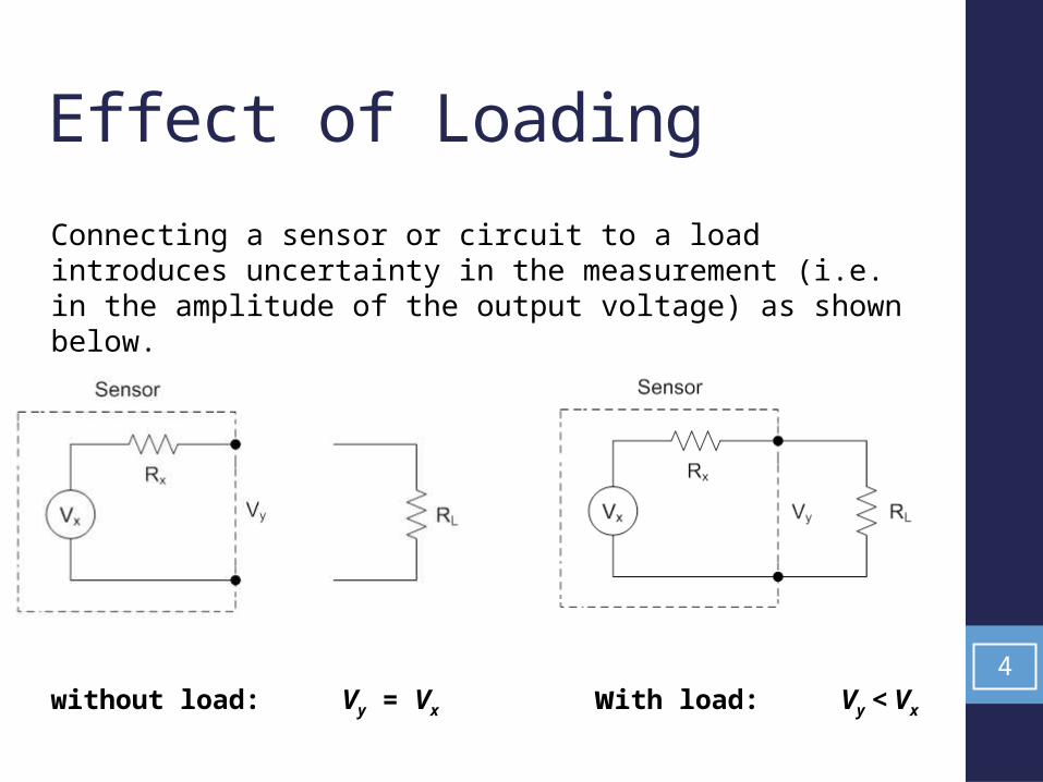
Connecting a sensor or circuit to a load introduces uncertainty in the measurement (i.e. in the amplitude of the output voltage) as shown below.
without load: Vy = Vx with load: Vy < Vx
Effect of Loading
4
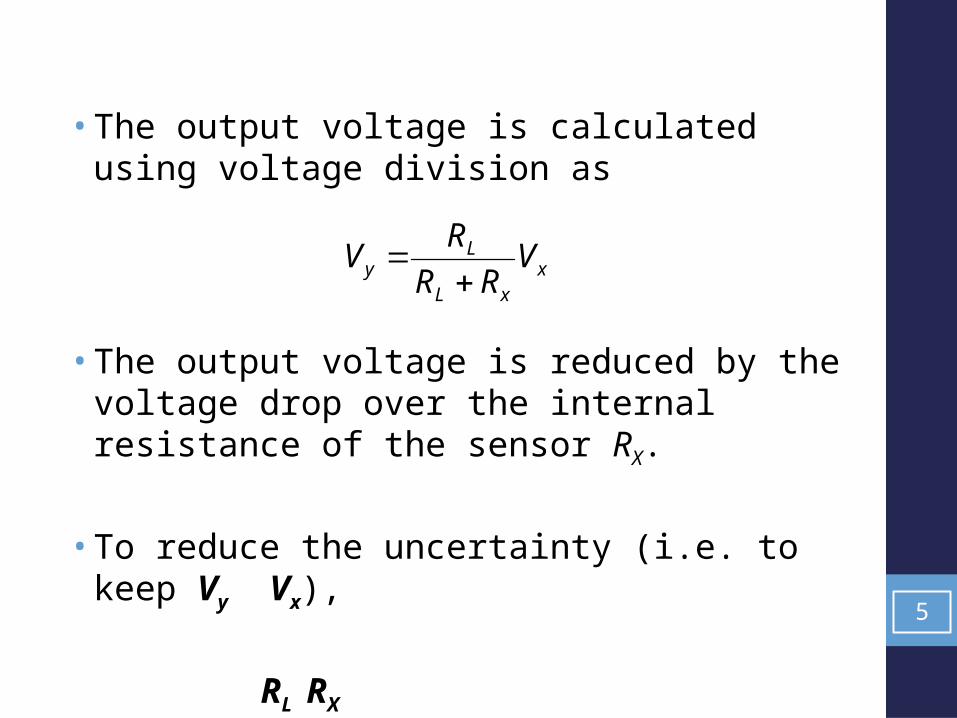
• The output voltage is calculated using voltage division as
• The output voltage is reduced by the voltage drop over the internal resistance of the sensor RX.
• To reduce the uncertainty (i.e. to keep Vy Vx),
RL RX
xxL
Ly V
RR
RV
5
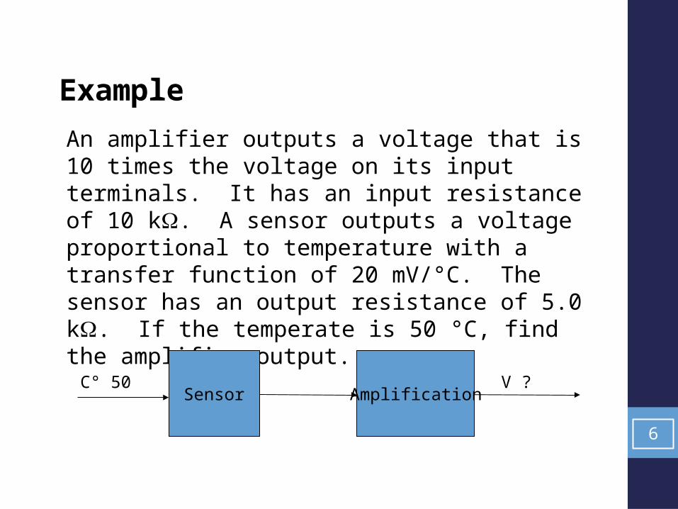
An amplifier outputs a voltage that is 10 times the voltage on its input terminals. It has an input resistance of 10 k. A sensor outputs a voltage proportional to temperature with a transfer function of 20 mV/°C. The sensor has an output resistance of 5.0 k. If the temperate is 50 °C, find the amplifier output.
Sensor50° C ?V
Amplification
Example
6
Answer
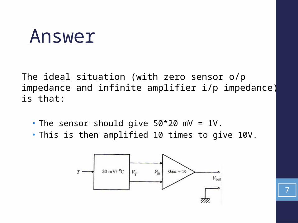
The ideal situation (with zero sensor o/p impedance and infinite amplifier i/p impedance) is that:
• The sensor should give 50*20 mV = 1V.• This is then amplified 10 times to give 10V.
7
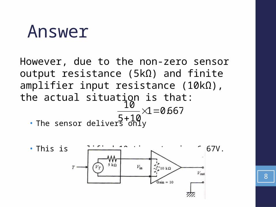
Answer However, due to the non-zero sensor output resistance (5kΩ) and finite amplifier input resistance (10kΩ), the actual situation is that:
• The sensor delivers only
• This is amplified 10 times to give 6.67V.
667.01105
10
8
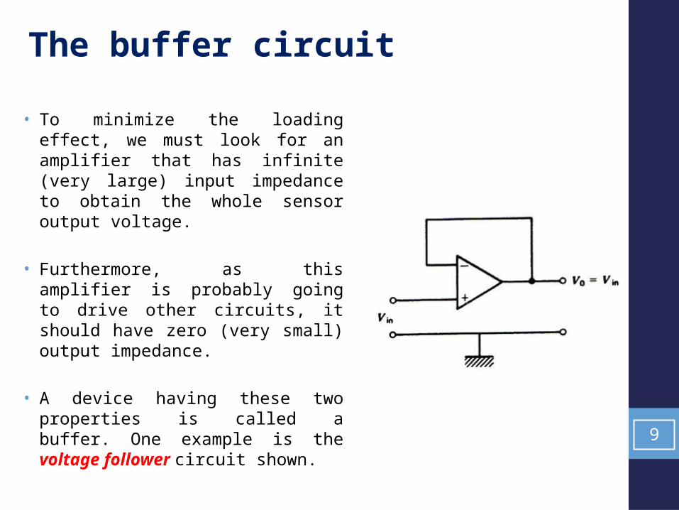
• To minimize the loading effect, we must look for an amplifier that has infinite (very large) input impedance to obtain the whole sensor output voltage.
• Furthermore, as this amplifier is probably going to drive other circuits, it should have zero (very small) output impedance.
• A device having these two properties is called a buffer. One example is the voltage follower circuit shown.
The buffer circuit
9
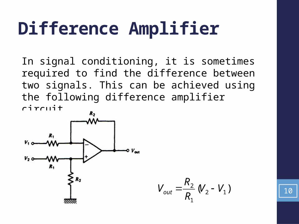
Difference Amplifier
In signal conditioning, it is sometimes required to find the difference between two signals. This can be achieved using the following difference amplifier circuit.
)( 121
2 VVR
RVout 10
The instrumentation amplifier
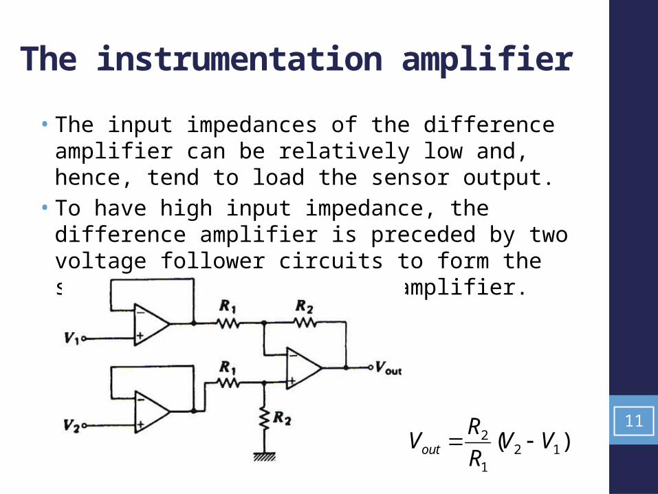
• The input impedances of the difference amplifier can be relatively low and, hence, tend to load the sensor output.
• To have high input impedance, the difference amplifier is preceded by two voltage follower circuits to form the so-called instrumentation amplifier.
)( 121
2 VVR
RVout
11
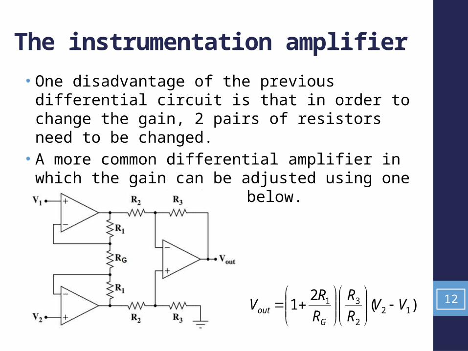
• One disadvantage of the previous differential circuit is that in order to change the gain, 2 pairs of resistors need to be changed.
• A more common differential amplifier in which the gain can be adjusted using one resistor (RG) is shown below.
)(2
1 122
31 VVR
R
R
RV
Gout
The instrumentation amplifier
12
Signal conditioning
Now, let us discuss the following signal conditioning categories:
Signal-range and offset changesi.e. amplification and zero adjustment
Linearization
Conversions e.g. current to voltage and voltage to current 13
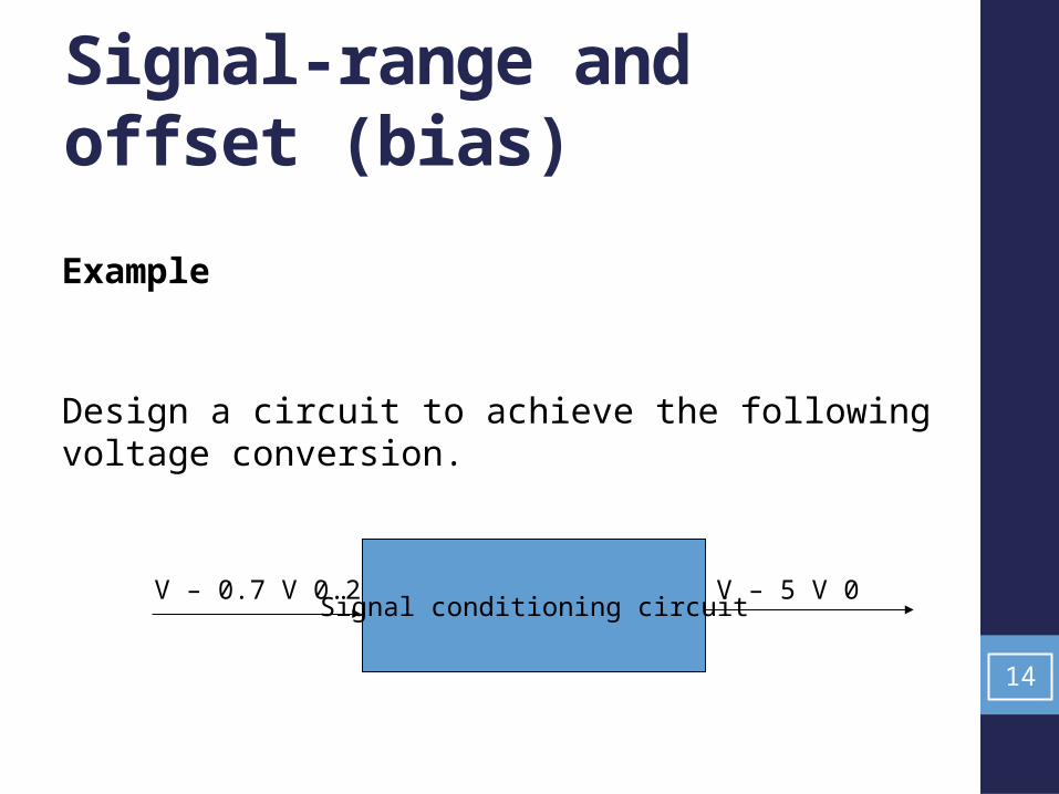
Signal-range and offset (bias)
Example
Design a circuit to achieve the following voltage conversion.
Signal conditioning circuit0.2 V – 0.7 V 0 V – 5 V
14
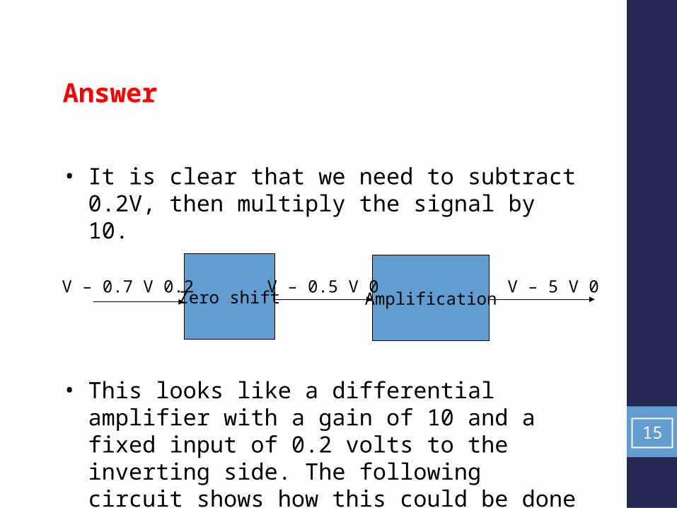
Zero shift0.2 V – 0.7 V 0 V – 5 V
Amplification0 V – 0.5 V
Answer
• It is clear that we need to subtract 0.2V, then multiply the signal by 10.
• This looks like a differential amplifier with a gain of 10 and a fixed input of 0.2 volts to the inverting side. The following circuit shows how this could be done using an instrumentation amplifier.
15
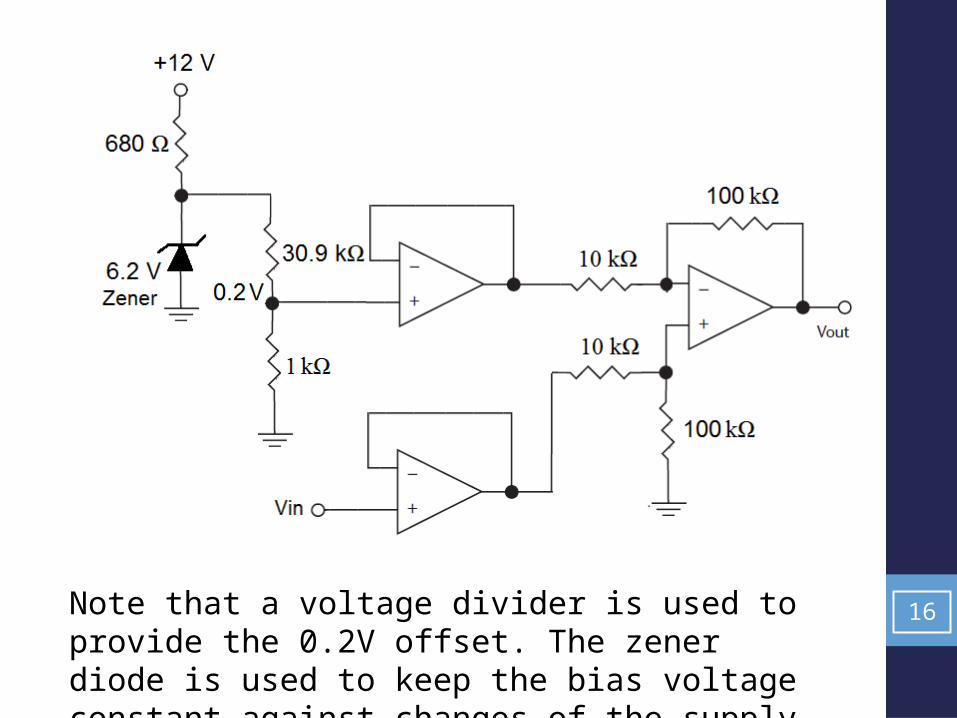
Note that a voltage divider is used to provide the 0.2V offset. The zener diode is used to keep the bias voltage constant against changes of the supply.
16
A sensor output a range of 20 to 250 mV as a variable varies over its range. Develop signal conditioning so that this become 0 to 5 V. The circuit must have very high input impedance.
AnswerLet us develop an linear equation for the output in terms of the input
Vout = aVin+b
where a and b are to be found.
Example 2-20 (Johnson, page 89)
17
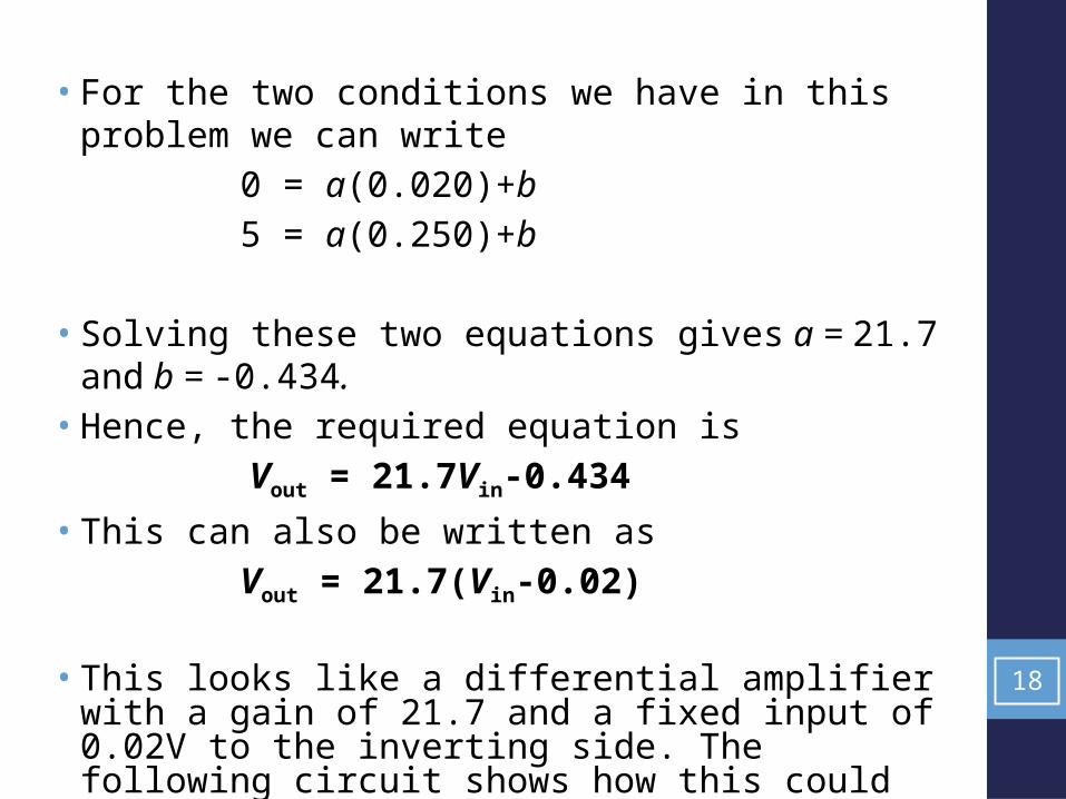
• For the two conditions we have in this problem we can write 0 = a(0.020)+b
5 = a(0.250)+b
• Solving these two equations gives a = 21.7 and b = -0.434. • Hence, the required equation is
Vout = 21.7Vin-0.434
• This can also be written asVout = 21.7(Vin-0.02)
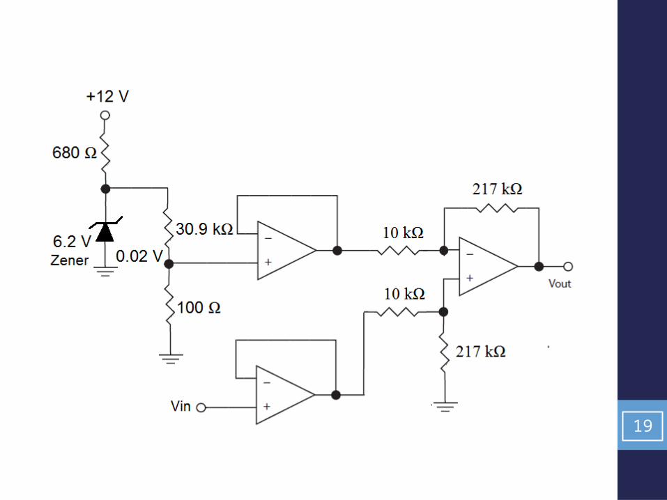
• This looks like a differential amplifier with a gain of 21.7 and a fixed input of 0.02V to the inverting side. The following circuit shows how this could be done using an instrumentation amplifier. 18
19
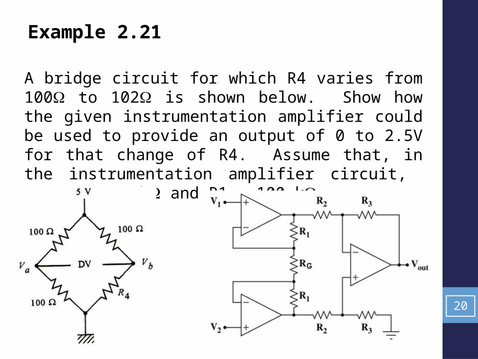
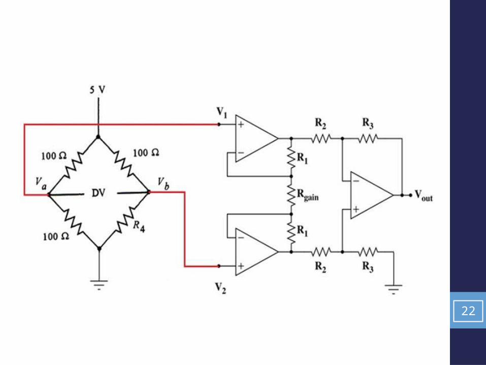
Example 2.21
A bridge circuit for which R4 varies from 100 to 102 is shown below. Show how the given instrumentation amplifier could be used to provide an output of 0 to 2.5V for that change of R4. Assume that, in the instrumentation amplifier circuit, R2 = R3 = 1 k and R1 = 100 k.
20
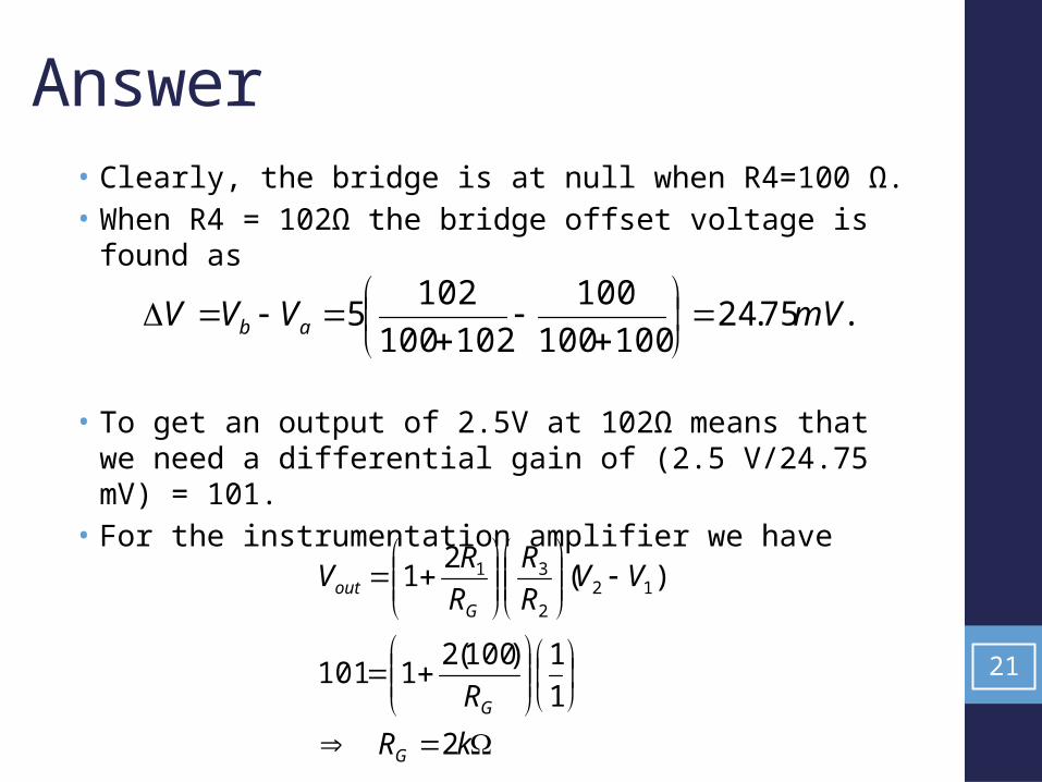
Answer• Clearly, the bridge is at null when R4=100 Ω. • When R4 = 102Ω the bridge offset voltage is found as
• To get an output of 2.5V at 102Ω means that we need a differential gain of (2.5 V/24.75 mV) = 101.
• For the instrumentation amplifier we have
.75.24100100
100
102100
1025 mVVVV ab
kR
R
VVR
R
R
RV
G
G
Gout
2
1
1)100(21101
)(2
1 122
31
21
22
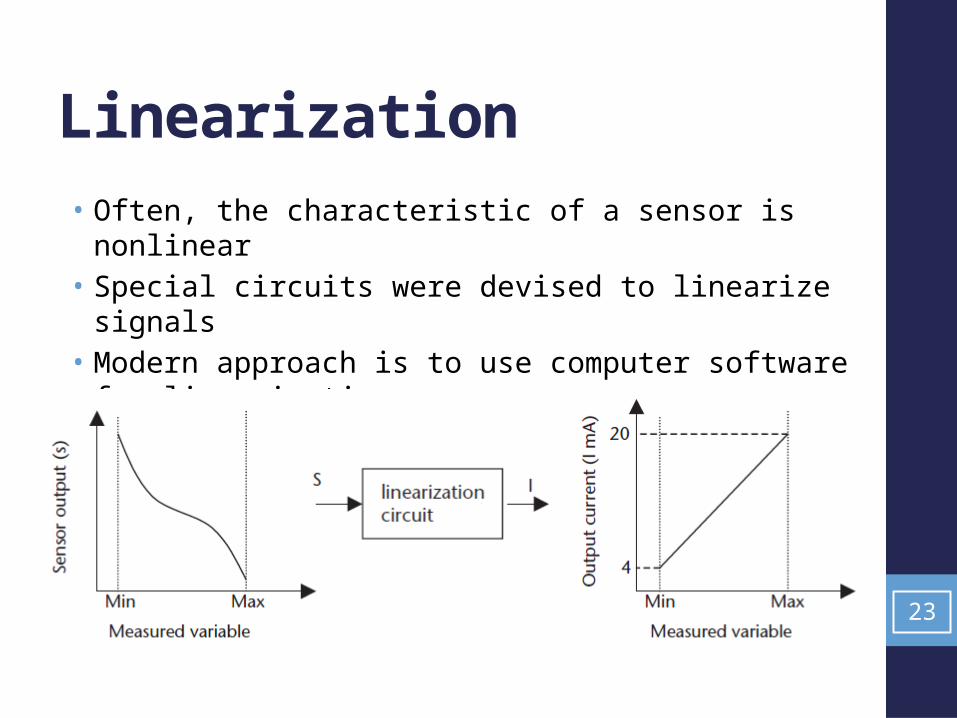
Linearization• Often, the characteristic of a sensor is nonlinear• Special circuits were devised to linearize signals• Modern approach is to use computer software for linearization.
23
Conversion In many situations it is required to convert one form of
signal or physical value into another form such aso resistance to voltageo voltage-to-current o current-to-voltage
A typical standard in process control systems is to use current signals in the range 4 to 20 mA for transmission. This requires conversion from voltage to current at the sending end and a conversion from current to voltage at the receiving end. 24
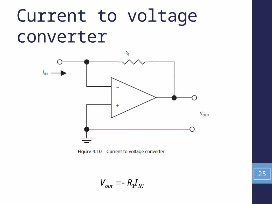
Current to voltage converter
25
INout IRV 1
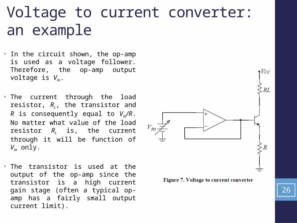
Voltage to current converter: an example
26
• In the circuit shown, the op-amp is used as a voltage follower. Therefore, the op-amp output voltage is Vin.
• The current through the load resistor, RL, the transistor and R is consequently equal to Vin/R. No matter what value of the load resistor RL is, the current through it will be function of Vin only.
• The transistor is used at the output of the op-amp since the transistor is a high current gain stage (often a typical op-amp has a fairly small output current limit).