Embed Size (px)
Citation preview
Lecture 7 - 1Introduction to Digital Integrated Circuit DesignMemory and Array Circuits
Lecture 7
Memory and Array Circuits
Konstantinos MasselosDepartment of Electrical & Electronic Engineering
Imperial College London
URL: http://cas.ee.ic.ac.uk/~kostasE-mail: [email protected]
Lecture 7 - 2Introduction to Digital Integrated Circuit DesignMemory and Array Circuits
Based on slides/material by…
J. Rabaey http://bwrc.eecs.berkeley.edu/Classes/IcBook/instructors.html“Digital Integrated Circuits: A Design Perspective”, Prentice Hall
D. Harris http://www.cmosvlsi.com/coursematerials.htmlWeste and Harris, “CMOS VLSI Design: A Circuits and Systems Perspective”, Addison Wesley
Lecture 7 - 3Introduction to Digital Integrated Circuit DesignMemory and Array Circuits
Recommended Reading
J. Rabaey et. al. “Digital Integrated Circuits: A Design Perspective”: Chapter 12
Weste and Harris, “CMOS VLSI Design: A Circuits and Systems Perspective”: Chapter 11
Lecture 7 - 4Introduction to Digital Integrated Circuit DesignMemory and Array Circuits
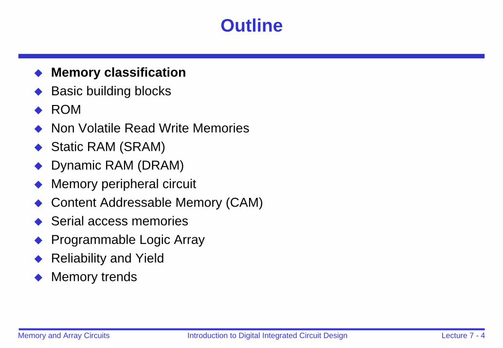
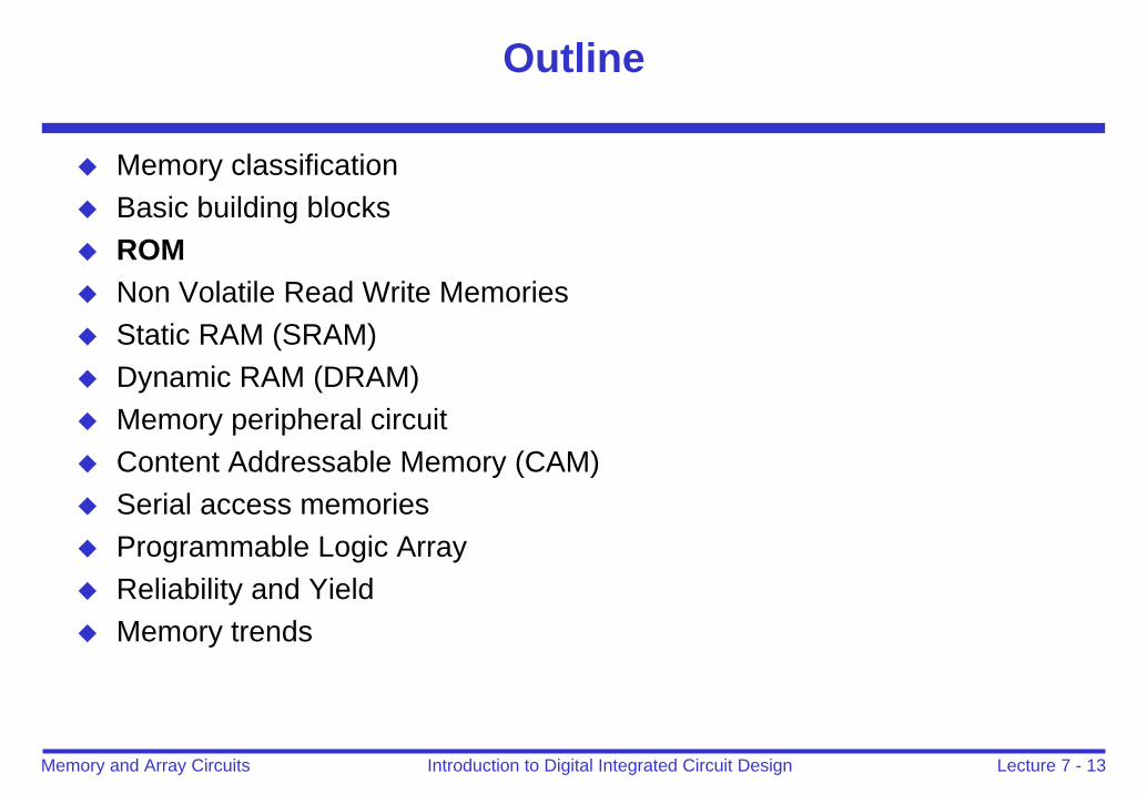
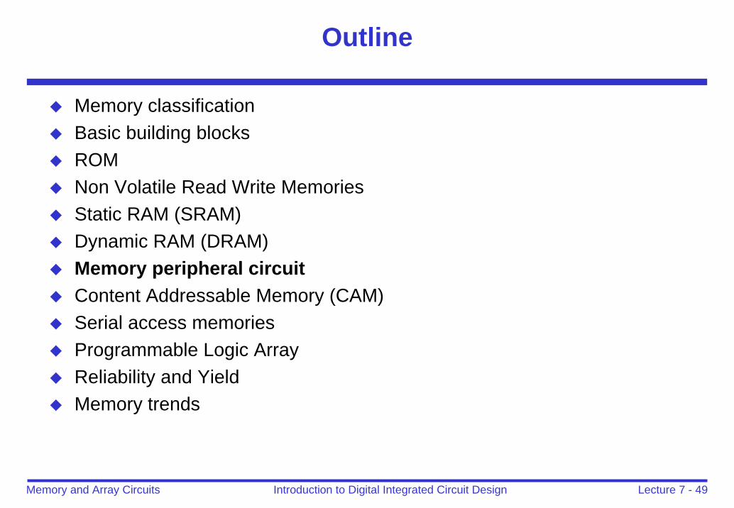
Outline
Memory classificationBasic building blocksROMNon Volatile Read Write MemoriesStatic RAM (SRAM)Dynamic RAM (DRAM)Memory peripheral circuitContent Addressable Memory (CAM)Serial access memoriesProgrammable Logic ArrayReliability and YieldMemory trends
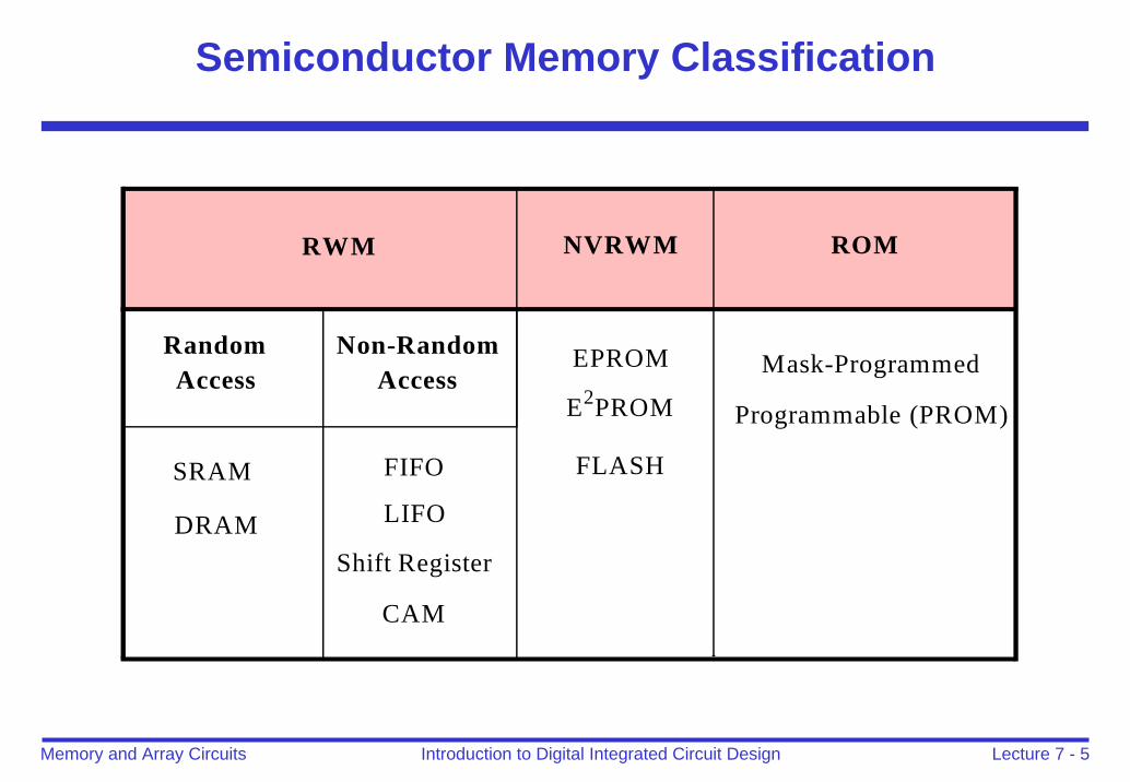
Lecture 7 - 5Introduction to Digital Integrated Circuit DesignMemory and Array Circuits
Semiconductor Memory Classification
RWM NVRWM ROM
EPROM
E2PROM
FLASH
RandomAccess
Non-RandomAccess
SRAM
DRAM
Mask-Programmed
Programmable (PROM)
FIFO
Shift Register
CAM
LIFO
Lecture 7 - 6Introduction to Digital Integrated Circuit DesignMemory and Array Circuits
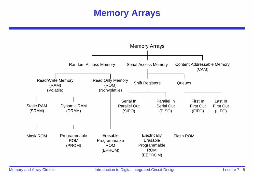
Memory Arrays
Memory Arrays
Random Access Memory Serial Access Memory Content Addressable Memory(CAM)
Read/Write Memory(RAM)
(Volatile)
Read Only Memory(ROM)
(Nonvolatile)
Static RAM(SRAM)
Dynamic RAM(DRAM)
Shift Registers Queues
First InFirst Out(FIFO)
Last InFirst Out(LIFO)
Serial InParallel Out
(SIPO)
Parallel InSerial Out
(PISO)
Mask ROM ProgrammableROM
(PROM)
ErasableProgrammable
ROM(EPROM)
ElectricallyErasable
ProgrammableROM
(EEPROM)
Flash ROM
Lecture 7 - 7Introduction to Digital Integrated Circuit DesignMemory and Array Circuits
Outline
Memory classificationBasic building blocksROMNon Volatile Read Write MemoriesStatic RAM (SRAM)Dynamic RAM (DRAM)Memory peripheral circuitContent Addressable Memory (CAM) Serial access memoriesProgrammable Logic ArrayReliability and YieldMemory trends
Lecture 7 - 8Introduction to Digital Integrated Circuit DesignMemory and Array Circuits
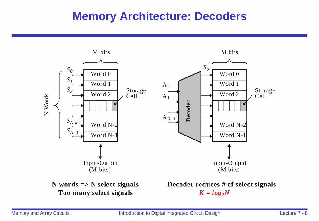
Memory Architecture: Decoders
Word 0Word 1
Word 2
Word N-1
Word N-2
Input-Output
S0
S1
S2
SN-2
SN_1
(M bits)
StorageCell
M bitsN
Wor
ds
Word 0Word 1
Word 2
Word N-1
Word N-2
Input-Output(M bits)
StorageCell
M bits
Dec
oder
A0
A1
AK -1
S0
N words => N select signalsToo many select signals
Decoder reduces # of select signalsK = log2N
Lecture 7 - 9Introduction to Digital Integrated Circuit DesignMemory and Array Circuits
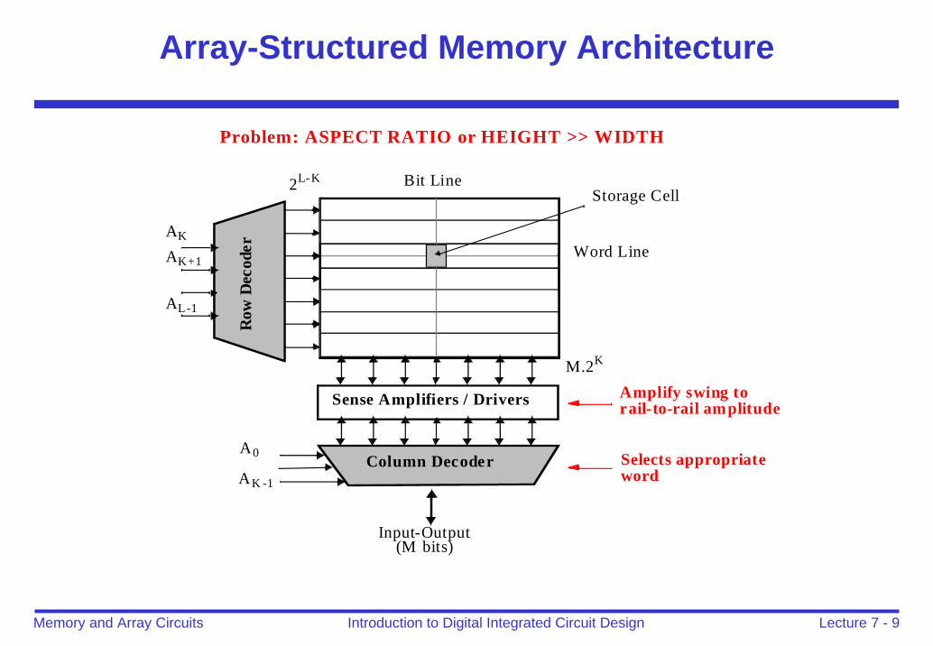
Array-Structured Memory Architecture
Input-Output(M bits)
Row
Dec
oder
AK
AK+1
AL-1
2L-K
Column Decoder
Bit Line
Word Line
A0
AK -1
Storage Cell
Sense Amplifiers / Drivers
M.2K
Problem: ASPECT RATIO or HEIGHT >> WIDTH
Amplify swing torail-to-rail amplitude
Selects appropriateword
Lecture 7 - 10Introduction to Digital Integrated Circuit DesignMemory and Array Circuits
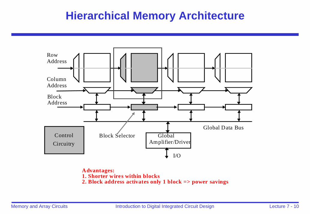
Hierarchical Memory Architecture
Global Data Bus
RowAddress
ColumnAddress
BlockAddress
Block Selector GlobalAmplifier/Driver
I/O
ControlCircuitry
Advantages:1. Shorter wires within blocks2. Block address activates only 1 block => power savings
Lecture 7 - 11Introduction to Digital Integrated Circuit DesignMemory and Array Circuits
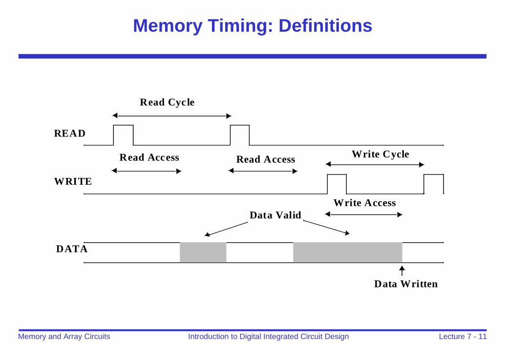
Memory Timing: Definitions
READ
WRITE
DATA
Read Access Read Access
Read Cycle
Data Valid
Data Written
Write Access
Write Cycle
Lecture 7 - 12Introduction to Digital Integrated Circuit DesignMemory and Array Circuits
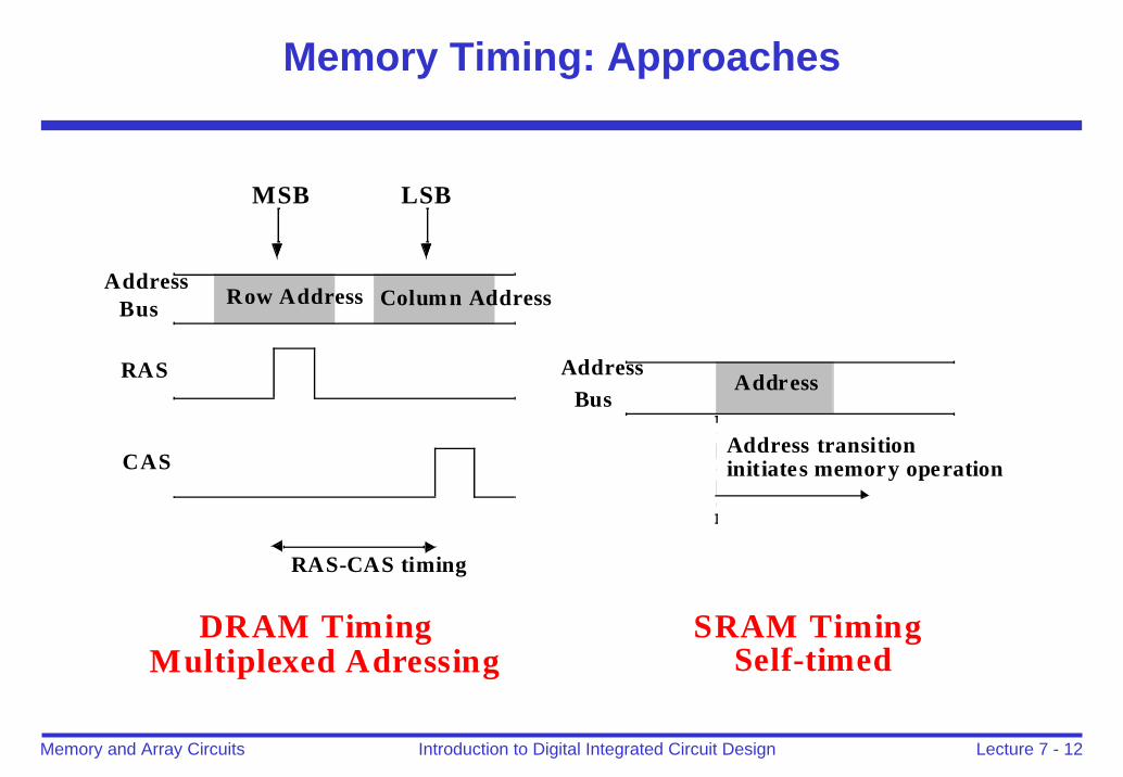
Memory Timing: Approaches
AddressBus
RAS
CAS
RAS-CAS timing
AddressBus
Address
Address transitioninitiates memory operation
DRAM Timing SRAM Timing
Row Address Column Address
MSB LSB
Multiplexed Adressing Self-timed
Lecture 7 - 13Introduction to Digital Integrated Circuit DesignMemory and Array Circuits
Outline
Memory classificationBasic building blocksROMNon Volatile Read Write MemoriesStatic RAM (SRAM)Dynamic RAM (DRAM)Memory peripheral circuitContent Addressable Memory (CAM)Serial access memoriesProgrammable Logic ArrayReliability and YieldMemory trends
Lecture 7 - 14Introduction to Digital Integrated Circuit DesignMemory and Array Circuits
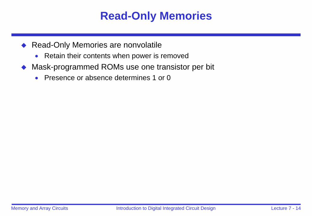
Read-Only Memories
Read-Only Memories are nonvolatile• Retain their contents when power is removed
Mask-programmed ROMs use one transistor per bit• Presence or absence determines 1 or 0
Lecture 7 - 15Introduction to Digital Integrated Circuit DesignMemory and Array Circuits
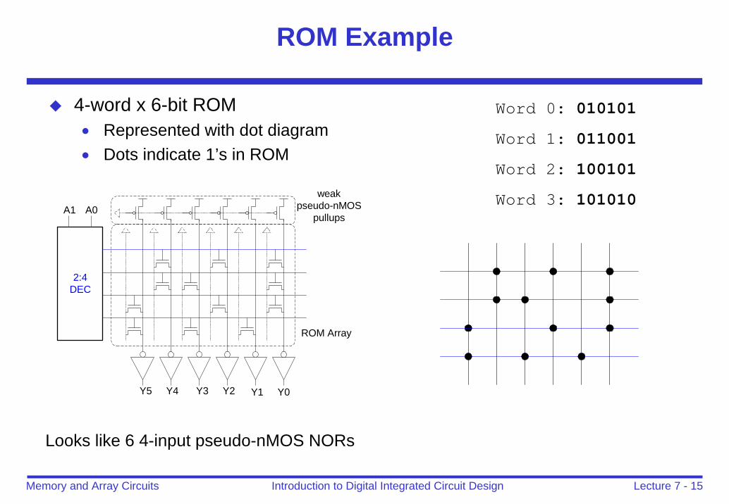
ROM Example
4-word x 6-bit ROM• Represented with dot diagram• Dots indicate 1’s in ROM
Word 0: 010101
Word 1: 011001
Word 2: 100101
Word 3: 101010
ROM Array
2:4DEC
A0A1
Y0Y1Y2Y3Y4Y5
weakpseudo-nMOS
pullups
Looks like 6 4-input pseudo-nMOS NORs
Lecture 7 - 16Introduction to Digital Integrated Circuit DesignMemory and Array Circuits
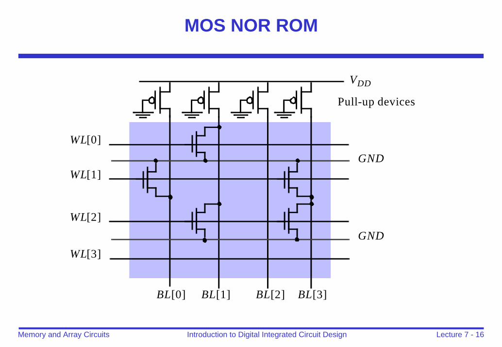
MOS NOR ROM
WL[0]
WL[1]
WL[2]
WL[3]
BL[0] BL[1] BL[2] BL[3]
GND
GND
VDD
Pull-up devices
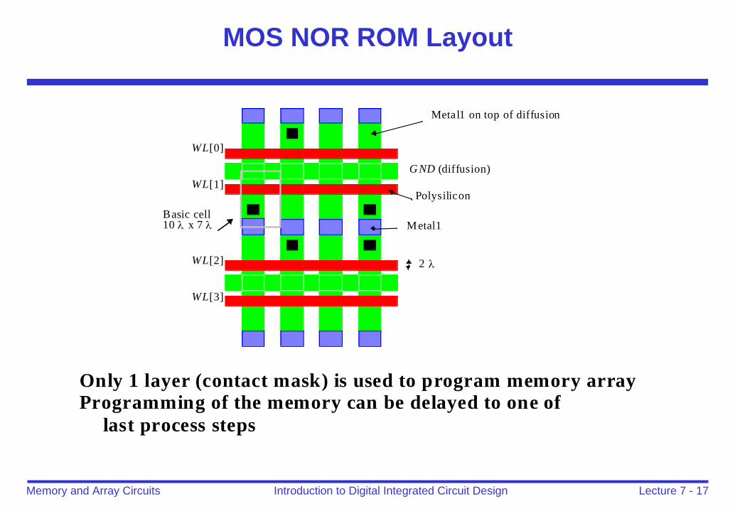
Lecture 7 - 17Introduction to Digital Integrated Circuit DesignMemory and Array Circuits
MOS NOR ROM Layout
Metal1 on top of diffusion
Basic cell10 λ x 7 λ
2 λ
WL[0]
WL[1]
WL[2]
WL[3]
GND (diffusion)
Metal1
Polysilicon
Only 1 layer (contact mask) is used to program memory arrayProgramming of the memory can be delayed to one of
last process steps
Lecture 7 - 18Introduction to Digital Integrated Circuit DesignMemory and Array Circuits
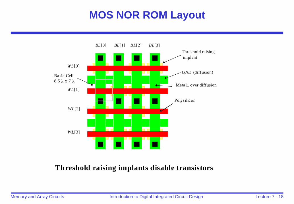
MOS NOR ROM Layout
Basic Cell8.5 λ x 7 λ
WL[0]
WL[1]
WL[2]
WL[3]
Metal1 over diffusion
Threshold raisingimplant
BL[0] BL[1] BL[2] BL[3]
Polysilicon
GND (diffusion)
Threshold raising implants disable transistors
Lecture 7 - 19Introduction to Digital Integrated Circuit DesignMemory and Array Circuits
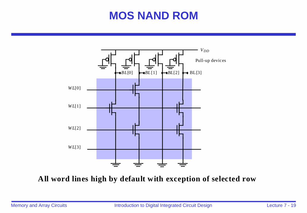
MOS NAND ROM
WL[0]
WL[1]
WL[2]
WL[3]
BL[0] BL [1] BL[2] BL[3]
VDD
Pull-up devices
All word lines high by default with exception of selected row
Lecture 7 - 20Introduction to Digital Integrated Circuit DesignMemory and Array Circuits
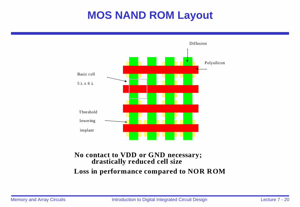
MOS NAND ROM Layout
Basic cell
5 λ x 6 λ
Threshold
implant
Polysilicon
Diffusion
lowering
No contact to VDD or GND necessary;
Loss in performance compared to NOR ROMdrastically reduced cell size
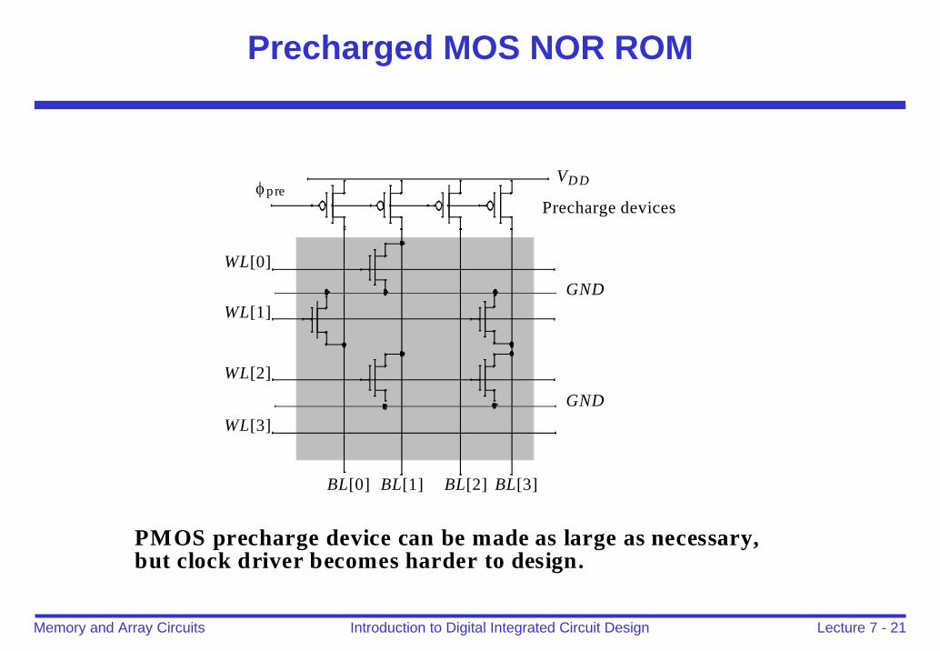
Lecture 7 - 21Introduction to Digital Integrated Circuit DesignMemory and Array Circuits
Precharged MOS NOR ROM
WL[0]
WL[1]
WL[2]
WL[3]
BL[0] BL[1] BL[2] BL[3]
GND
GND
VDD
Precharge devicesφpre
PMOS precharge device can be made as large as necessary,but clock driver becomes harder to design.
Lecture 7 - 22Introduction to Digital Integrated Circuit DesignMemory and Array Circuits
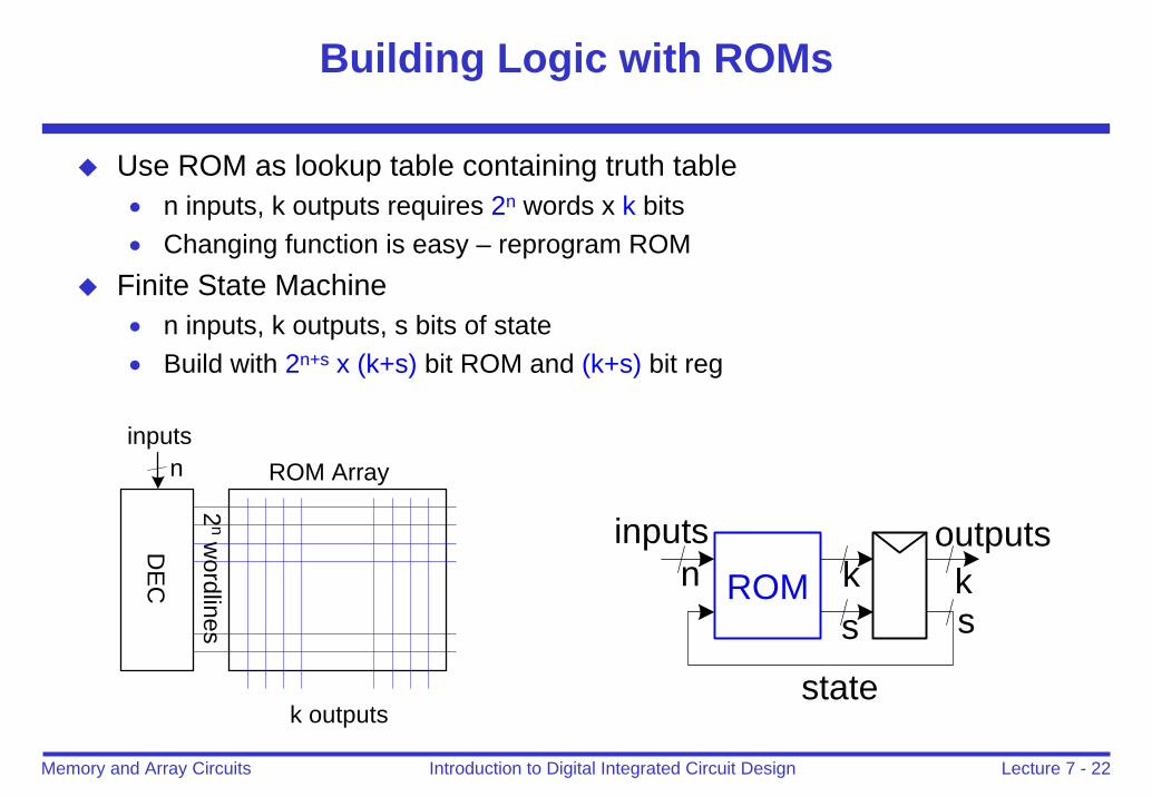
Building Logic with ROMs
Use ROM as lookup table containing truth table• n inputs, k outputs requires 2n words x k bits• Changing function is easy – reprogram ROM
Finite State Machine• n inputs, k outputs, s bits of state• Build with 2n+s x (k+s) bit ROM and (k+s) bit reg
ninputs
2n w
ordlines
ROM Array
k outputs
DE
C ROMinputs outputs
state
n ks
ks
Lecture 7 - 23Introduction to Digital Integrated Circuit DesignMemory and Array Circuits
Outline
Memory classificationBasic building blocksROMNon Volatile Read Write MemoriesStatic RAM (SRAM)Dynamic RAM (DRAM)Memory peripheral circuitContent Addressable Memory (CAM)Serial access memoriesProgrammable Logic ArrayReliability and YieldMemory trends
Lecture 7 - 24Introduction to Digital Integrated Circuit DesignMemory and Array Circuits
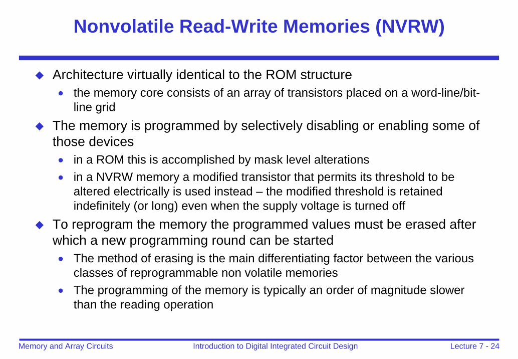
Nonvolatile Read-Write Memories (NVRW)
Architecture virtually identical to the ROM structure • the memory core consists of an array of transistors placed on a word-line/bit-
line gridThe memory is programmed by selectively disabling or enabling some of those devices
• in a ROM this is accomplished by mask level alterations• in a NVRW memory a modified transistor that permits its threshold to be
altered electrically is used instead – the modified threshold is retained indefinitely (or long) even when the supply voltage is turned off
To reprogram the memory the programmed values must be erased after which a new programming round can be started
• The method of erasing is the main differentiating factor between the various classes of reprogrammable non volatile memories
• The programming of the memory is typically an order of magnitude slower than the reading operation
Lecture 7 - 25Introduction to Digital Integrated Circuit DesignMemory and Array Circuits
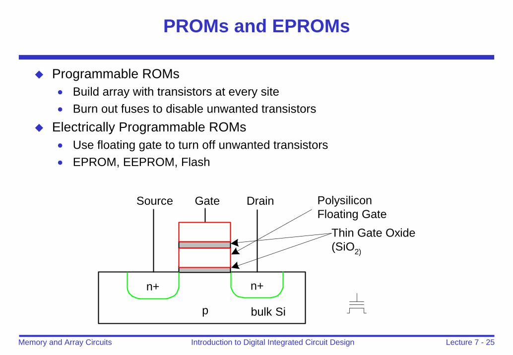
PROMs and EPROMs
Programmable ROMs• Build array with transistors at every site• Burn out fuses to disable unwanted transistors
Electrically Programmable ROMs• Use floating gate to turn off unwanted transistors• EPROM, EEPROM, Flash
n+
p
GateSource Drain
bulk Si
Thin Gate Oxide(SiO2)
n+
PolysiliconFloating Gate
Lecture 7 - 26Introduction to Digital Integrated Circuit DesignMemory and Array Circuits
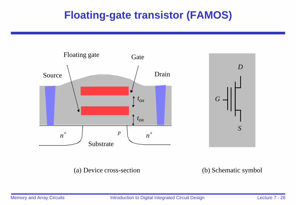
Floating-gate transistor (FAMOS)
Source Drain
GateFloating gate
tox
tox
Substraten+n+ p
(a) Device cross-section
S
D
G
(b) Schematic symbol
Lecture 7 - 27Introduction to Digital Integrated Circuit DesignMemory and Array Circuits
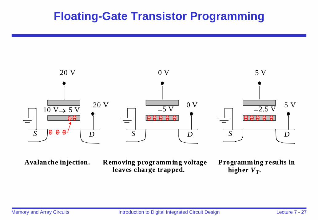
Floating-Gate Transistor Programming
DS
20 V
20 V
DS
0 V
0 V10 V→ 5 V −5 V
DS
5 V
5 V−2.5 V
Avalanche injection. Removing programming voltageleaves charge trapped.
Programming results inhigher VT.
Lecture 7 - 28Introduction to Digital Integrated Circuit DesignMemory and Array Circuits
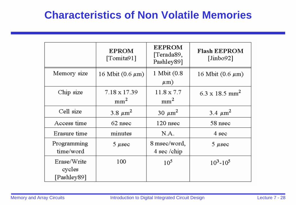
Characteristics of Non Volatile Memories
Lecture 7 - 29Introduction to Digital Integrated Circuit DesignMemory and Array Circuits
Outline
Memory classificationBasic building blocksROMNon Volatile Read Write MemoriesStatic RAM (SRAM)Dynamic RAM (DRAM)Memory peripheral circuitContent Addressable Memory (CAM)Serial access memoriesProgrammable Logic ArrayReliability and YieldMemory trends
Lecture 7 - 30Introduction to Digital Integrated Circuit DesignMemory and Array Circuits
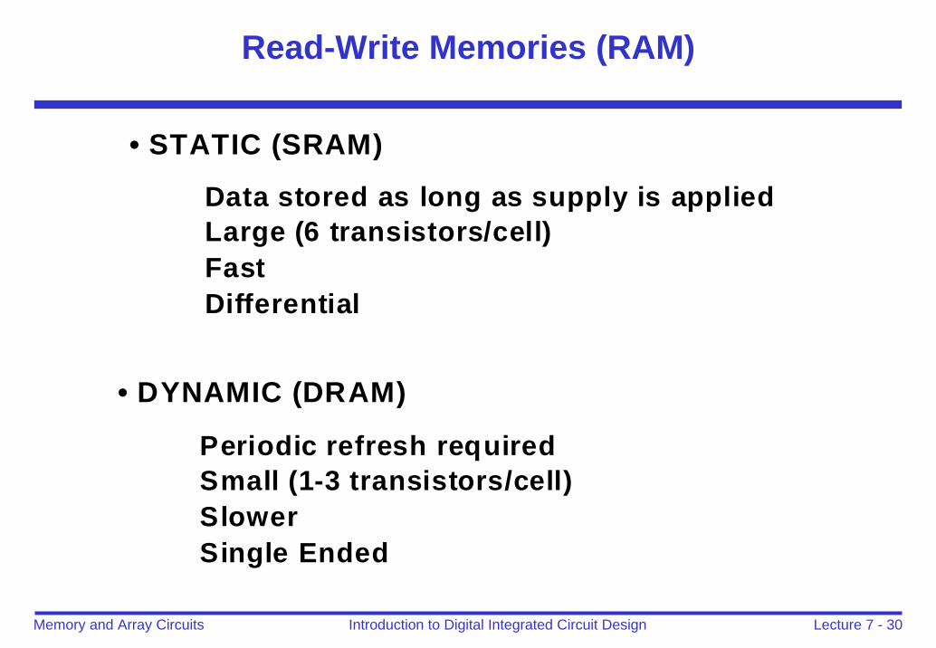
Read-Write Memories (RAM)
• STATIC (SRAM)
• DYNAMIC (DRAM)
Data stored as long as supply is appliedLarge (6 transistors/cell)FastDifferential
Periodic refresh requiredSmall (1-3 transistors/cell)SlowerSingle Ended
Lecture 7 - 31Introduction to Digital Integrated Circuit DesignMemory and Array Circuits
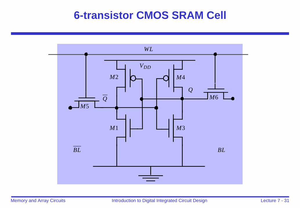
6-transistor CMOS SRAM Cell
VDD
M1 M3
M4M2
M5
BL
WL
BL
M6
Lecture 7 - 32Introduction to Digital Integrated Circuit DesignMemory and Array Circuits
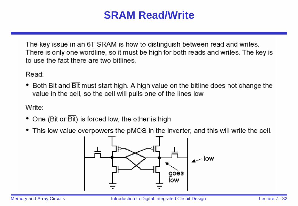
SRAM Read/Write
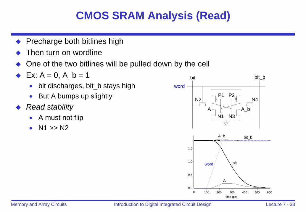
Lecture 7 - 33Introduction to Digital Integrated Circuit DesignMemory and Array Circuits
CMOS SRAM Analysis (Read)
bit bit_b
N1
N2P1
A
P2
N3
N4
A_b
word
0.0
0.5
1.0
1.5
0 100 200 300 400 500 600time (ps)
word bit
A
A_b bit_b
Precharge both bitlines highThen turn on wordlineOne of the two bitlines will be pulled down by the cellEx: A = 0, A_b = 1• bit discharges, bit_b stays high• But A bumps up slightly
Read stability• A must not flip• N1 >> N2
Lecture 7 - 34Introduction to Digital Integrated Circuit DesignMemory and Array Circuits
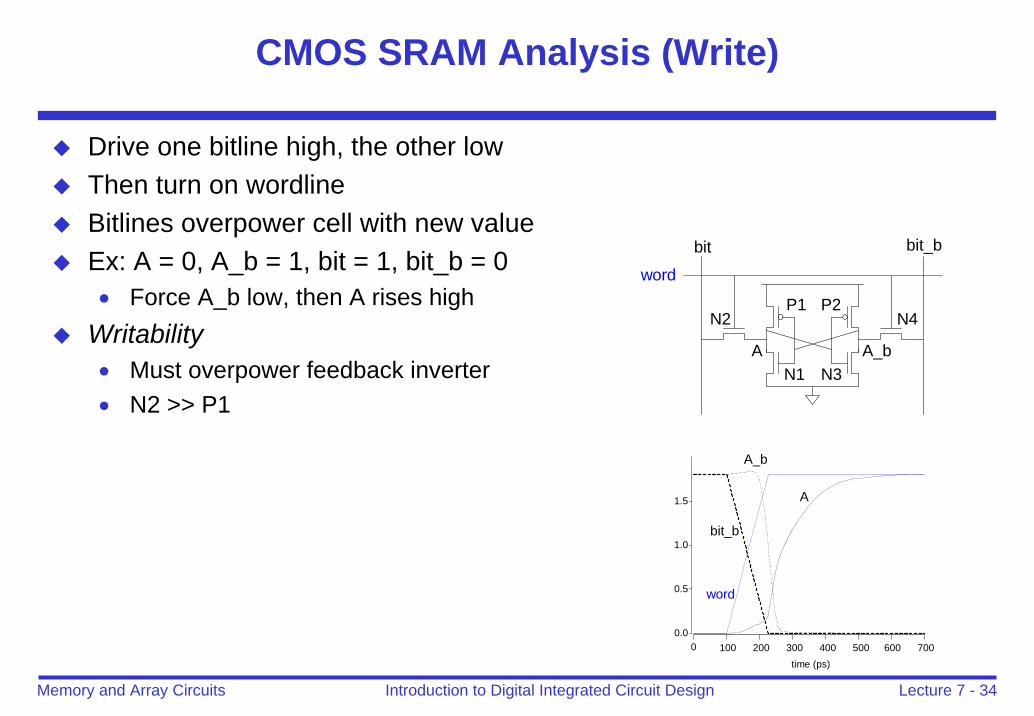
CMOS SRAM Analysis (Write)
Drive one bitline high, the other lowThen turn on wordlineBitlines overpower cell with new valueEx: A = 0, A_b = 1, bit = 1, bit_b = 0• Force A_b low, then A rises high
Writability• Must overpower feedback inverter• N2 >> P1
time (ps)
word
A
A_b
bit_b
0.0
0.5
1.0
1.5
0 100 200 300 400 500 600 700
bit bit_b
N1
N2P1
A
P2
N3
N4
A_b
word
Lecture 7 - 35Introduction to Digital Integrated Circuit DesignMemory and Array Circuits
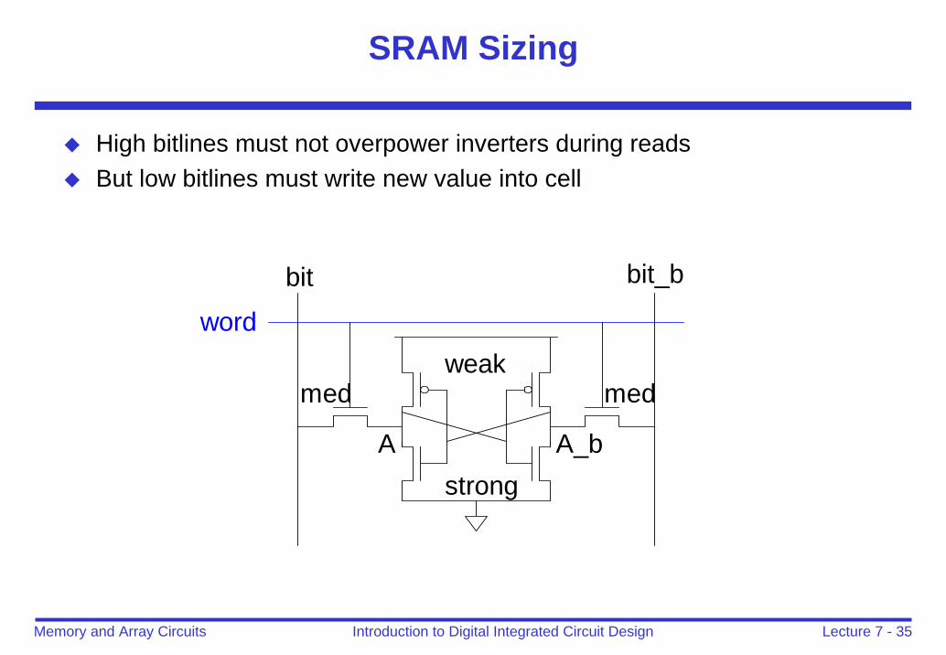
SRAM Sizing
High bitlines must not overpower inverters during readsBut low bitlines must write new value into cell
bit bit_b
med
A
weak
strong
med
A_b
word
Lecture 7 - 36Introduction to Digital Integrated Circuit DesignMemory and Array Circuits
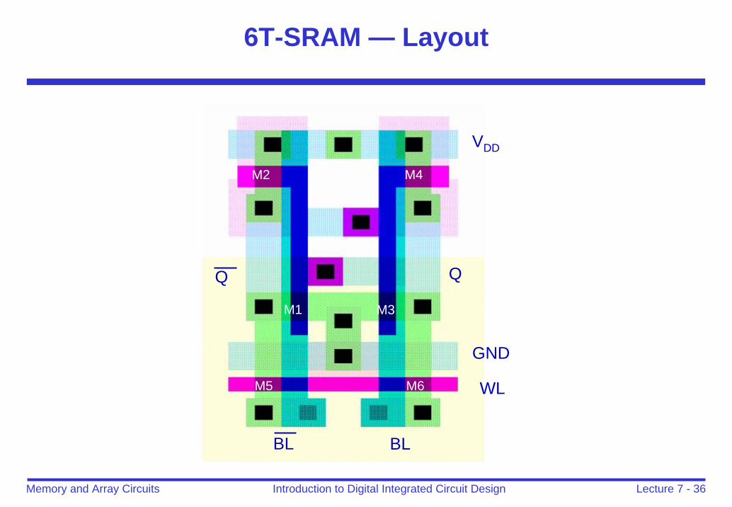
6T-SRAM — Layout
VDD
GND
WL
BLBL
M1 M3
M4M2
M5 M6
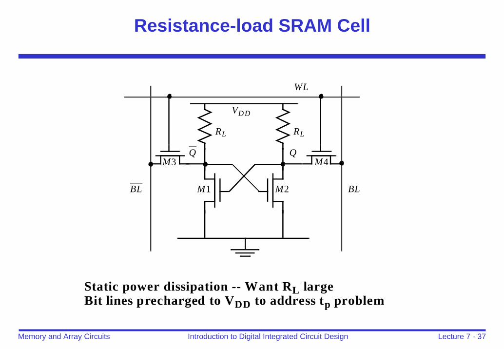
Lecture 7 - 37Introduction to Digital Integrated Circuit DesignMemory and Array Circuits
Resistance-load SRAM Cell
VDD
M1 M2
M3
BL
WL
BL
M4
RL RL
Static power dissipation -- Want RL largeBit lines precharged to VDD to address tp problem
Lecture 7 - 38Introduction to Digital Integrated Circuit DesignMemory and Array Circuits
Multiple Ports
We have considered single-ported SRAM• One read or one write on each cycle
Multiported SRAM are needed for register filesExamples:• Multicycle MIPS must read two sources or write a result on some cycles• Pipelined MIPS must read two sources and write a third result each cycle• Superscalar MIPS must read and write many sources and results each cycle
Lecture 7 - 39Introduction to Digital Integrated Circuit DesignMemory and Array Circuits
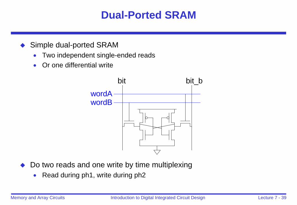
Dual-Ported SRAM
Simple dual-ported SRAM• Two independent single-ended reads• Or one differential write
Do two reads and one write by time multiplexing• Read during ph1, write during ph2
bit bit_b
wordBwordA
Lecture 7 - 40Introduction to Digital Integrated Circuit DesignMemory and Array Circuits
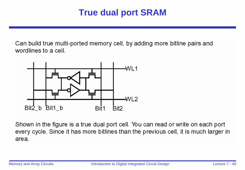
True dual port SRAM
Lecture 7 - 41Introduction to Digital Integrated Circuit DesignMemory and Array Circuits
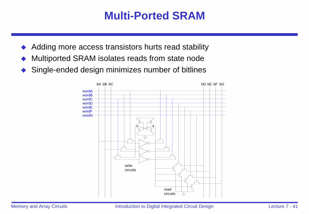
Multi-Ported SRAM
Adding more access transistors hurts read stabilityMultiported SRAM isolates reads from state nodeSingle-ended design minimizes number of bitlines
bA
wordBwordA
wordDwordC
wordFwordE
wordG
bB bC
writecircuits
readcircuits
bD bE bF bG
Lecture 7 - 42Introduction to Digital Integrated Circuit DesignMemory and Array Circuits
Outline
Memory classificationBasic building blocksROMNon Volatile Read Write MemoriesStatic RAM (SRAM)Dynamic RAM (DRAM)Memory peripheral circuitContent Addressable Memory (CAM)Serial access memoriesProgrammable Logic ArrayReliability and YieldMemory trends
Lecture 7 - 43Introduction to Digital Integrated Circuit DesignMemory and Array Circuits
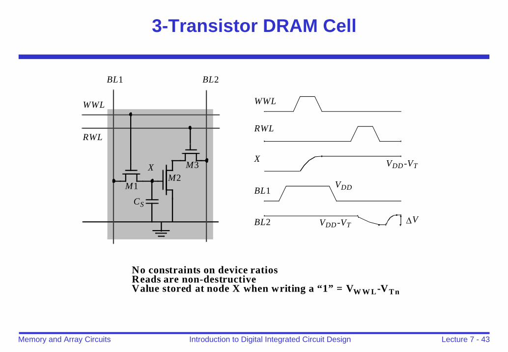
3-Transistor DRAM Cell
M2M1
BL1
WWL
BL2
M3
RWL
CS
X
WWL
RWL
X
BL1
BL2
VDD-VT
ΔV
VDD
VDD-VT
No constraints on device ratiosReads are non-destructiveValue stored at node X when writing a “1” = VW W L-VT n
Lecture 7 - 44Introduction to Digital Integrated Circuit DesignMemory and Array Circuits
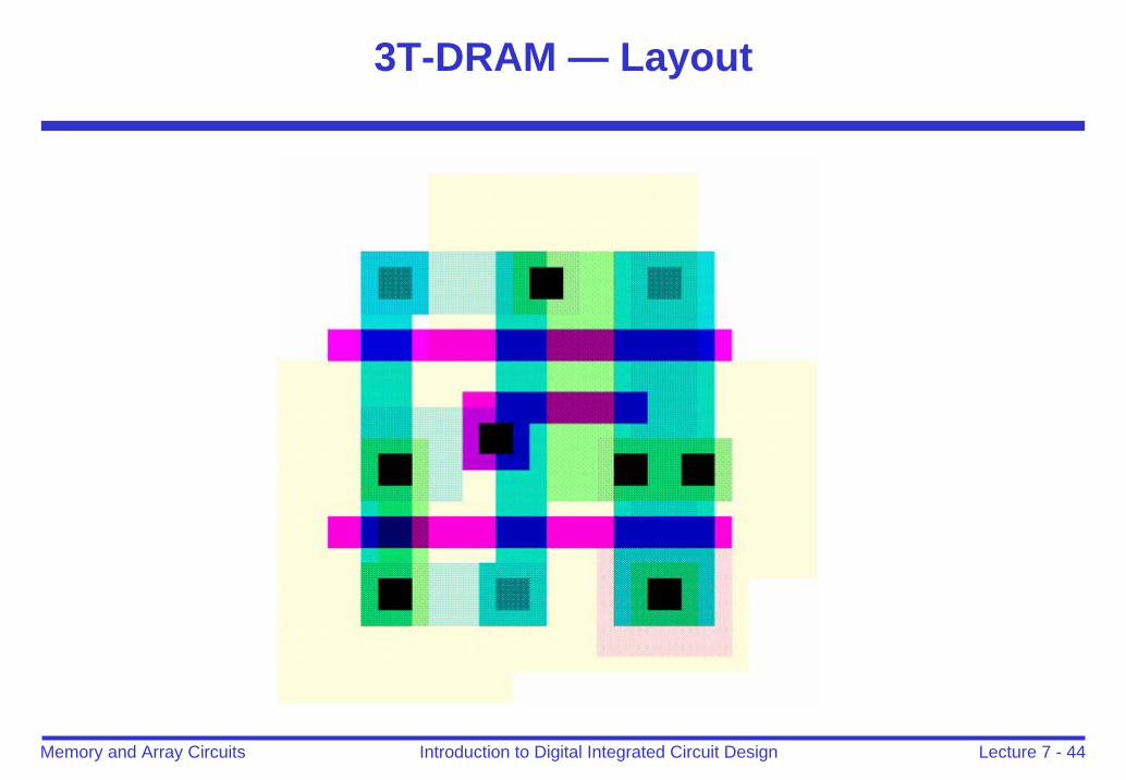
3T-DRAM — Layout
Lecture 7 - 45Introduction to Digital Integrated Circuit DesignMemory and Array Circuits
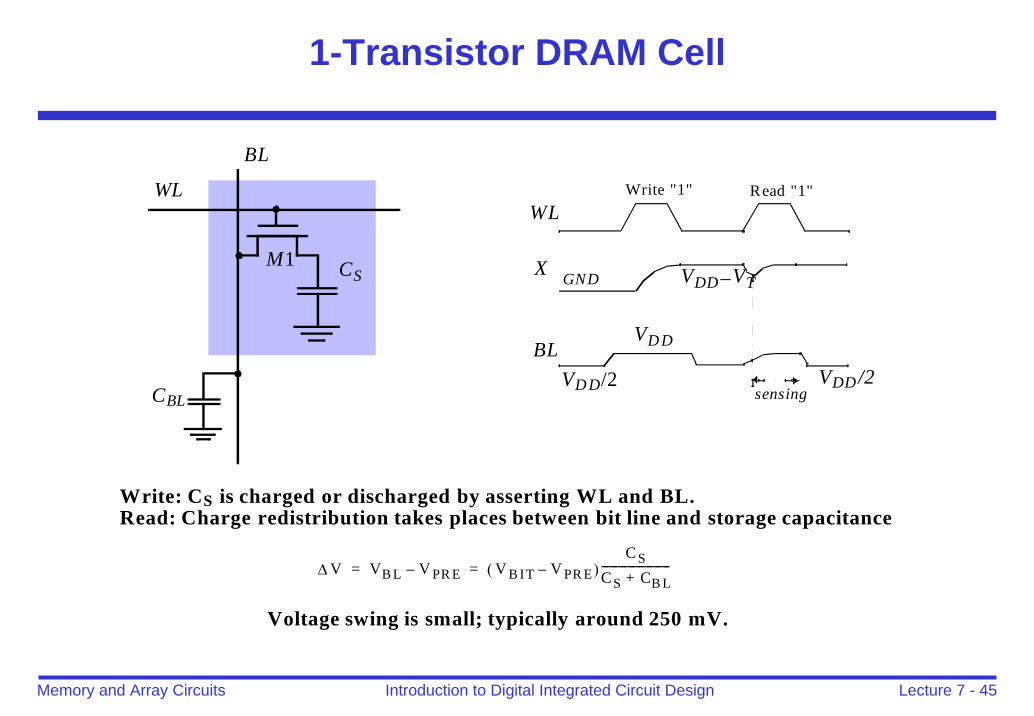
1-Transistor DRAM Cell
CSM1
BL
WL
CBL
WL
X
BL
VDD−VT
VDD/2
VDD
GND
Write "1" Read "1"
sensingVDD/2
Δ V VB L V PR E– V B IT V PR E–( )CS
CS CB L+------------------------= =
Write: CS is charged or discharged by asserting WL and BL.Read: Charge redistribution takes places between bit line and storage capacitance
Voltage swing is small; typically around 250 mV.
Lecture 7 - 46Introduction to Digital Integrated Circuit DesignMemory and Array Circuits
DRAM Cell Observations
1T DRAM requires a sense amplifier for each bit line, due to charge redistribution read-out.
DRAM memory cells are single ended in contrast to SRAM cells.
The read-out of the 1T DRAM cell is destructive; read and refresh operations are necessary for correct operation.
Unlike 3T cell, 1T cell requires presence of an extra capacitance that must be explicitly included in the design.
When writing a “1” into a DRAM cell, a threshold voltage is lost. This charge loss can be circumvented by bootstrapping the word lines to a higher value than VD D .
Lecture 7 - 47Introduction to Digital Integrated Circuit DesignMemory and Array Circuits
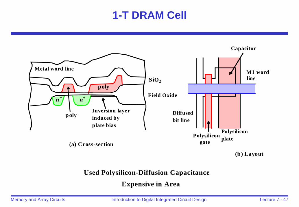
1-T DRAM Cell
(a) Cross-section
(b) Layout
Diffusedbit line
Polysiliconplate
M1 wordline
Capacitor
Polysilicongate
Metal word line
SiO2
n+ Field Oxide
Inversion layerinduced by plate bias
n+
poly
poly
Used Polysilicon-Diffusion Capacitance
Expensive in Area
Lecture 7 - 48Introduction to Digital Integrated Circuit DesignMemory and Array Circuits
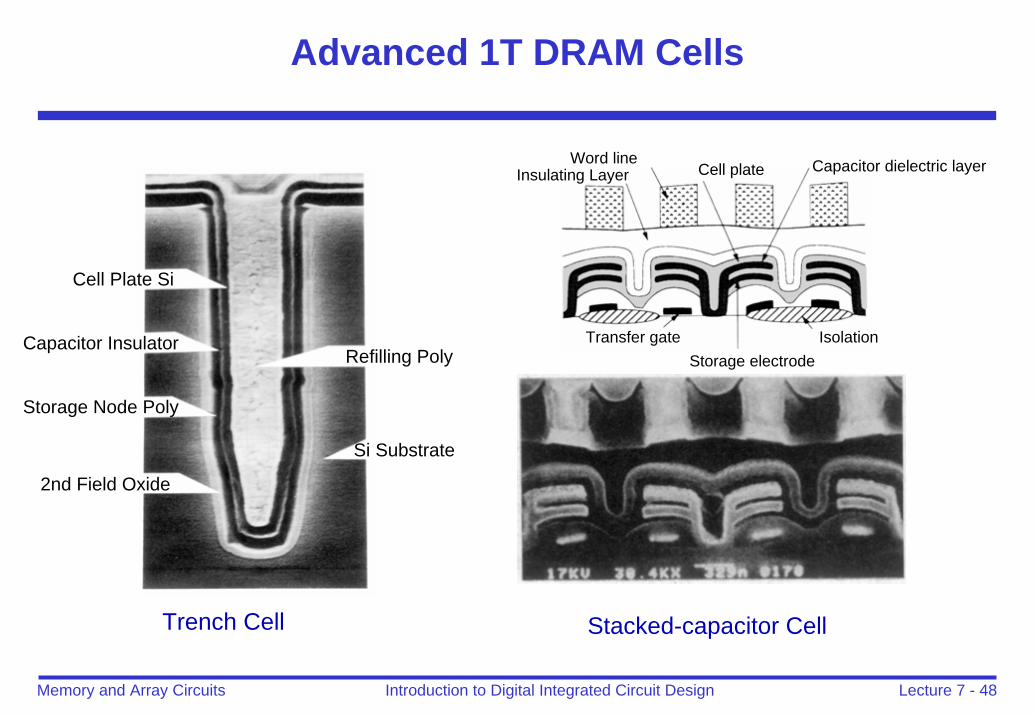
Advanced 1T DRAM Cells
Cell Plate Si
Capacitor Insulator
Storage Node Poly
2nd Field Oxide
Refilling Poly
Si Substrate
Trench Cell Stacked-capacitor Cell
Capacitor dielectric layerCell plateWord line
Insulating Layer
IsolationTransfer gateStorage electrode
Lecture 7 - 49Introduction to Digital Integrated Circuit DesignMemory and Array Circuits
Outline
Memory classificationBasic building blocksROMNon Volatile Read Write MemoriesStatic RAM (SRAM)Dynamic RAM (DRAM)Memory peripheral circuitContent Addressable Memory (CAM)Serial access memoriesProgrammable Logic ArrayReliability and YieldMemory trends
Lecture 7 - 50Introduction to Digital Integrated Circuit DesignMemory and Array Circuits
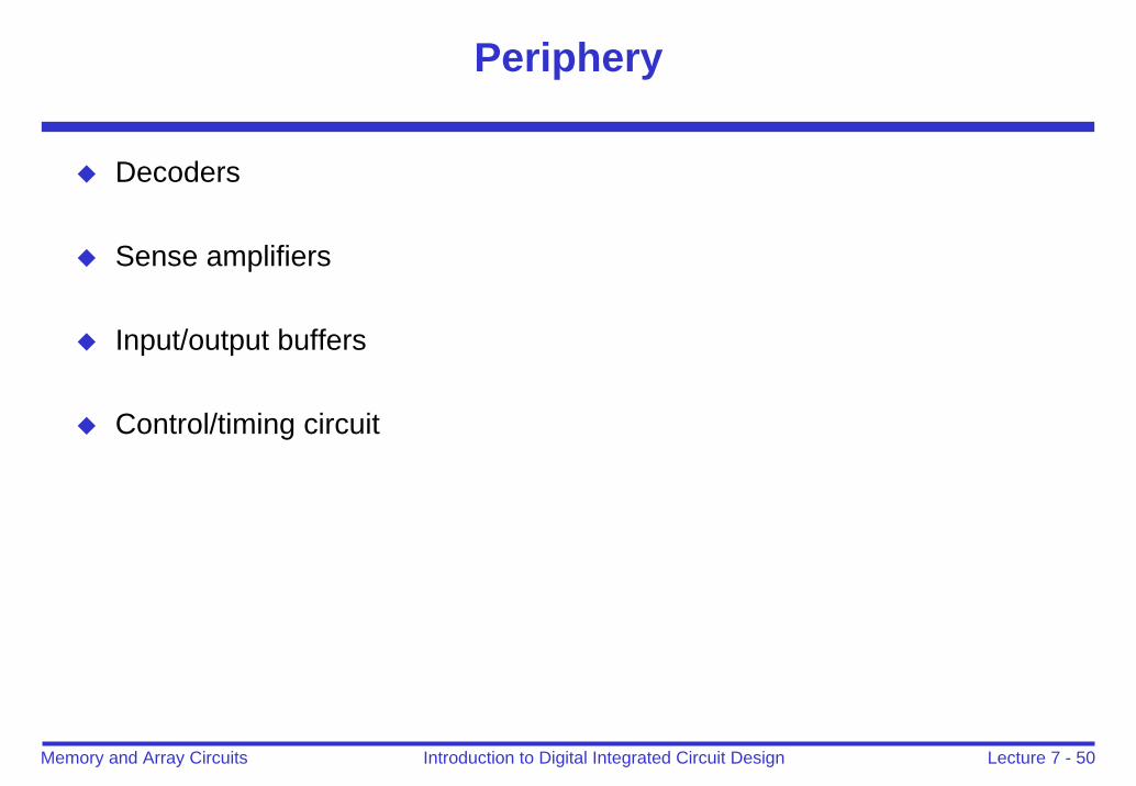
Periphery
Decoders
Sense amplifiers
Input/output buffers
Control/timing circuit
Lecture 7 - 51Introduction to Digital Integrated Circuit DesignMemory and Array Circuits
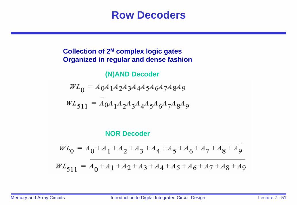
Row Decoders
Collection of 2M complex logic gatesOrganized in regular and dense fashion
(N)AND Decoder
NOR Decoder
Lecture 7 - 52Introduction to Digital Integrated Circuit DesignMemory and Array Circuits
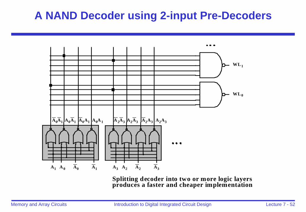
A NAND Decoder using 2-input Pre-Decoders
A0A1 A0A1 A0A1 A0A 1 A 2A3 A2A3 A2A3 A2A3
A1 A 0 A0 A1 A3 A2 A2 A3
WL0
WL1
Splitting decoder into two or more logic layersproduces a faster and cheaper implementation
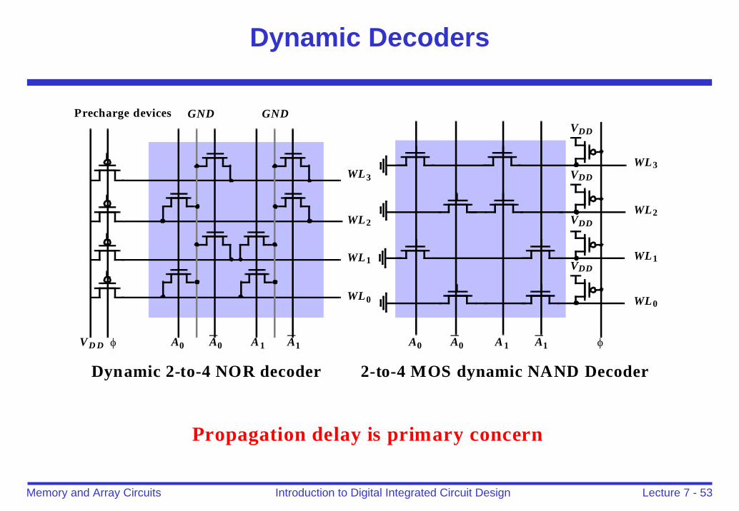
Lecture 7 - 53Introduction to Digital Integrated Circuit DesignMemory and Array Circuits
Dynamic Decoders
WL3
GND GNDPrecharge devices
WL2
WL1
WL0
VD D φ A0 A0 A1 A1 A0 A0 A1 A1
VDD
VDD
VDD
VDD
φ
WL3
WL2
WL1
WL0
Dynamic 2-to-4 NOR decoder 2-to-4 MOS dynamic NAND Decoder
Propagation delay is primary concern
Lecture 7 - 54Introduction to Digital Integrated Circuit DesignMemory and Array Circuits
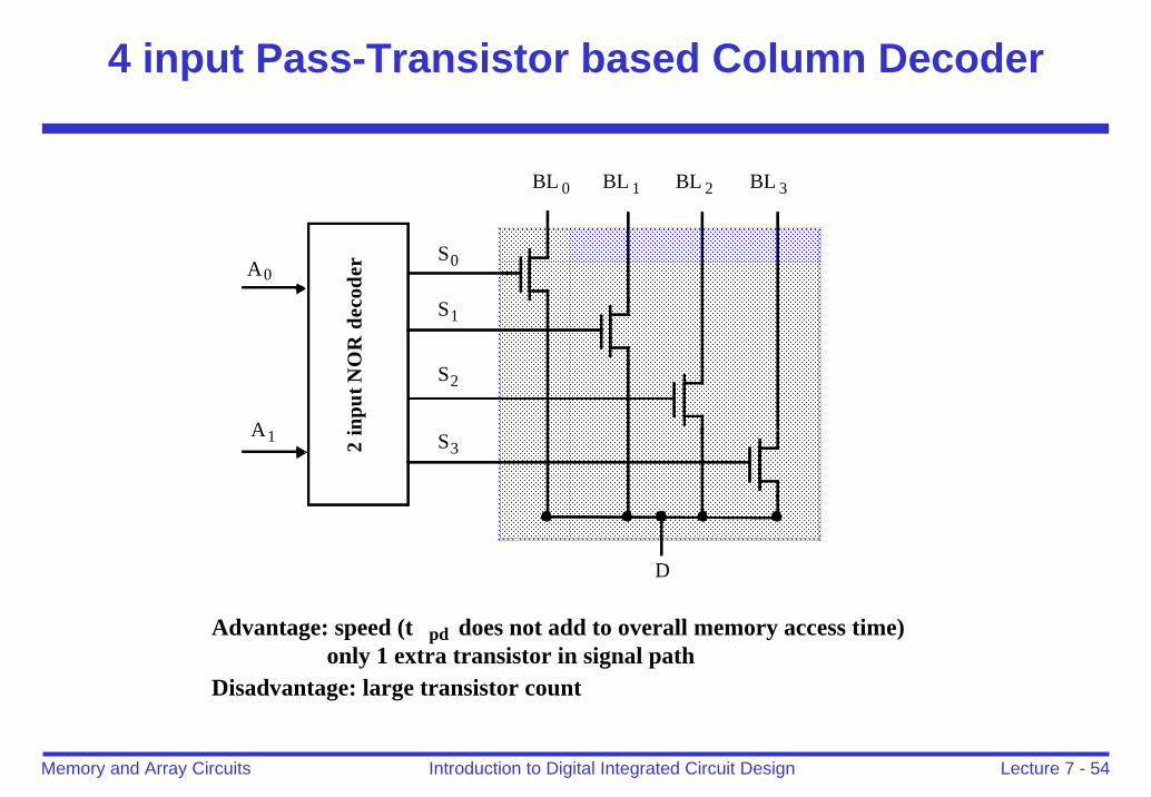
4 input Pass-Transistor based Column Decoder
BL 0 BL 1 BL 2 BL 3
D
A0
A1
S0
S1
S2
S32in
putN
OR
deco
der
Advantage: speed (t pd does not add to overall memory access time)
Disadvantage: large transistor countonly 1 extra transistor in signal path
Lecture 7 - 55Introduction to Digital Integrated Circuit DesignMemory and Array Circuits
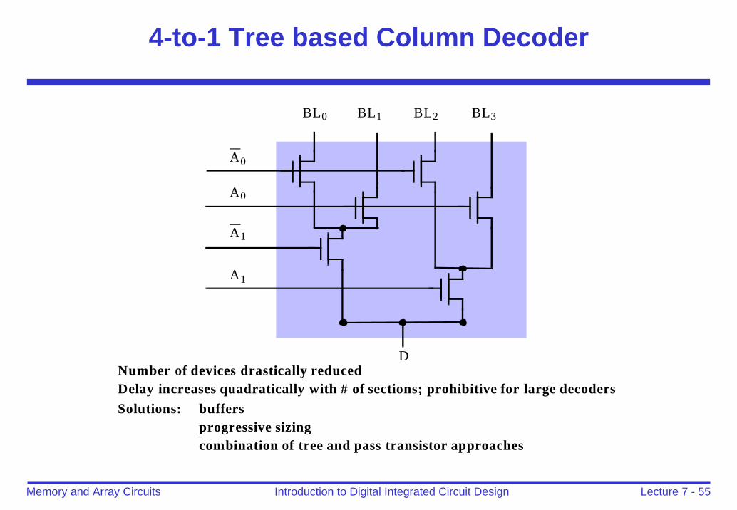
4-to-1 Tree based Column Decoder
BL0 BL1 BL2 BL3
D
A0
A0
A1
A1
Number of devices drastically reducedDelay increases quadratically with # of sections; prohibitive for large decoders
buffersprogressive sizingcombination of tree and pass transistor approaches
Solutions:
Lecture 7 - 56Introduction to Digital Integrated Circuit DesignMemory and Array Circuits
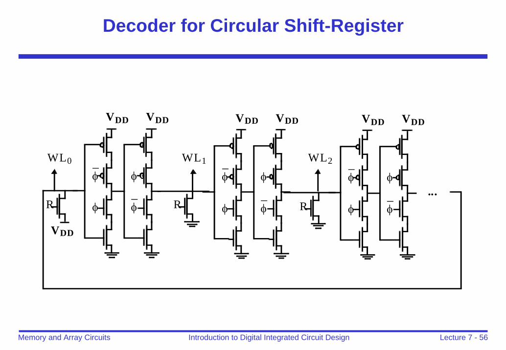
Decoder for Circular Shift-Register
φ
φ φ
φ
VDDVDD
φ
φ φ
φ
VDDVDD
φ
φ φ
φ
VDDVDD
RRR
VDD
...
WL0 WL1 WL2
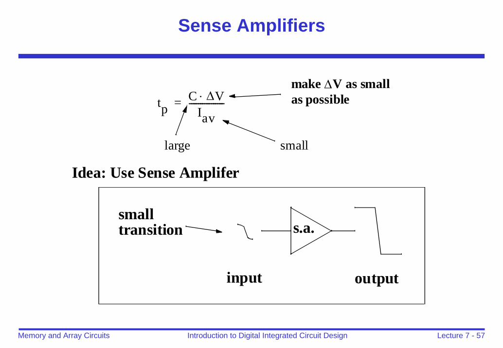
Lecture 7 - 57Introduction to Digital Integrated Circuit DesignMemory and Array Circuits
Sense Amplifiers
tpC ΔV⋅
Iav----------------=
make ΔV as smallas possible
smalllarge
Idea: Use Sense Amplifer
outputinput
s.a.smalltransition
Lecture 7 - 58Introduction to Digital Integrated Circuit DesignMemory and Array Circuits
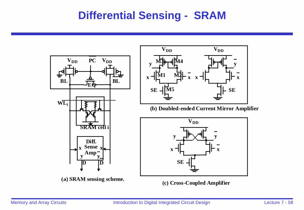
Differential Sensing - SRAM
Diff.SenseAmp
BLBL
SRAM cell i
x xy yD D
VDDVDD
WLi
PC
EQ
VDD
x x
y
SE
VDD
xx
y
SE
VDD
x x
y
SE
(b) Doubled-ended Current Mirror Amplifier
y
(a) SRAM sensing scheme.(c) Cross-Coupled Amplifier
M1 M2
M4M3
M5
Lecture 7 - 59Introduction to Digital Integrated Circuit DesignMemory and Array Circuits
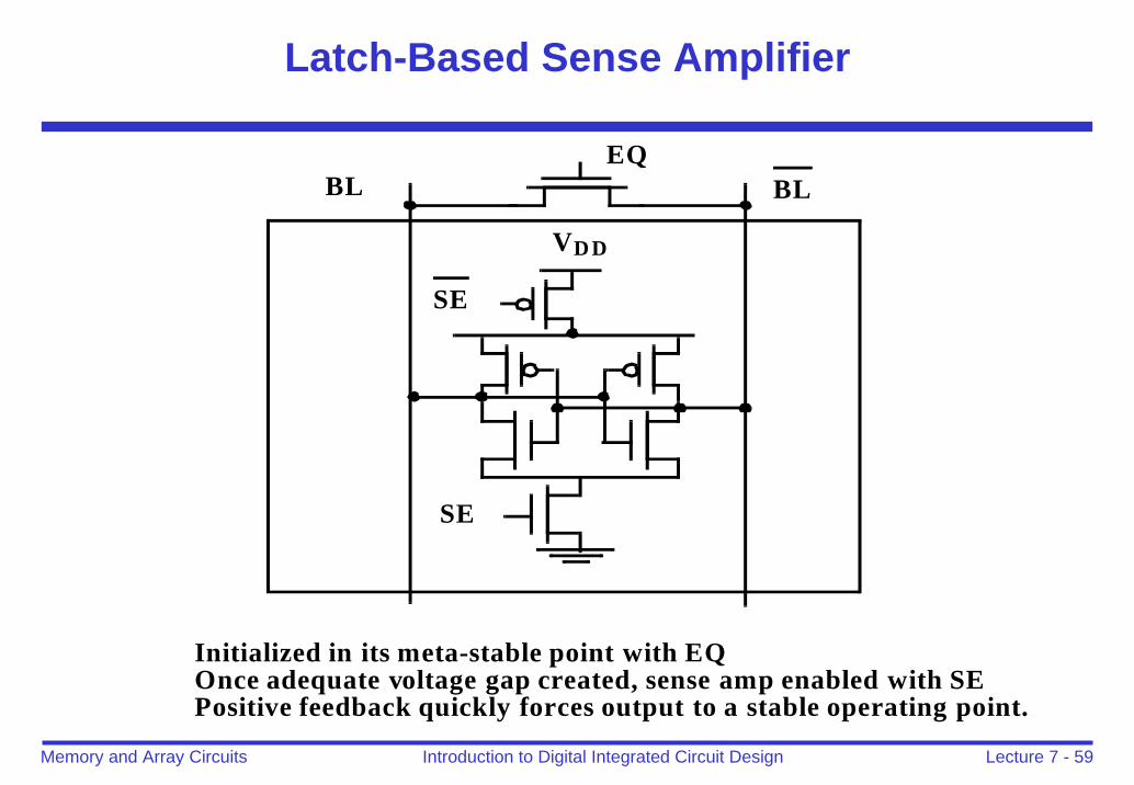
Latch-Based Sense Amplifier
VD D
BL
SE
SE
BLEQ
Initialized in its meta-stable point with EQOnce adequate voltage gap created, sense amp enabled with SEPositive feedback quickly forces output to a stable operating point.
Lecture 7 - 60Introduction to Digital Integrated Circuit DesignMemory and Array Circuits
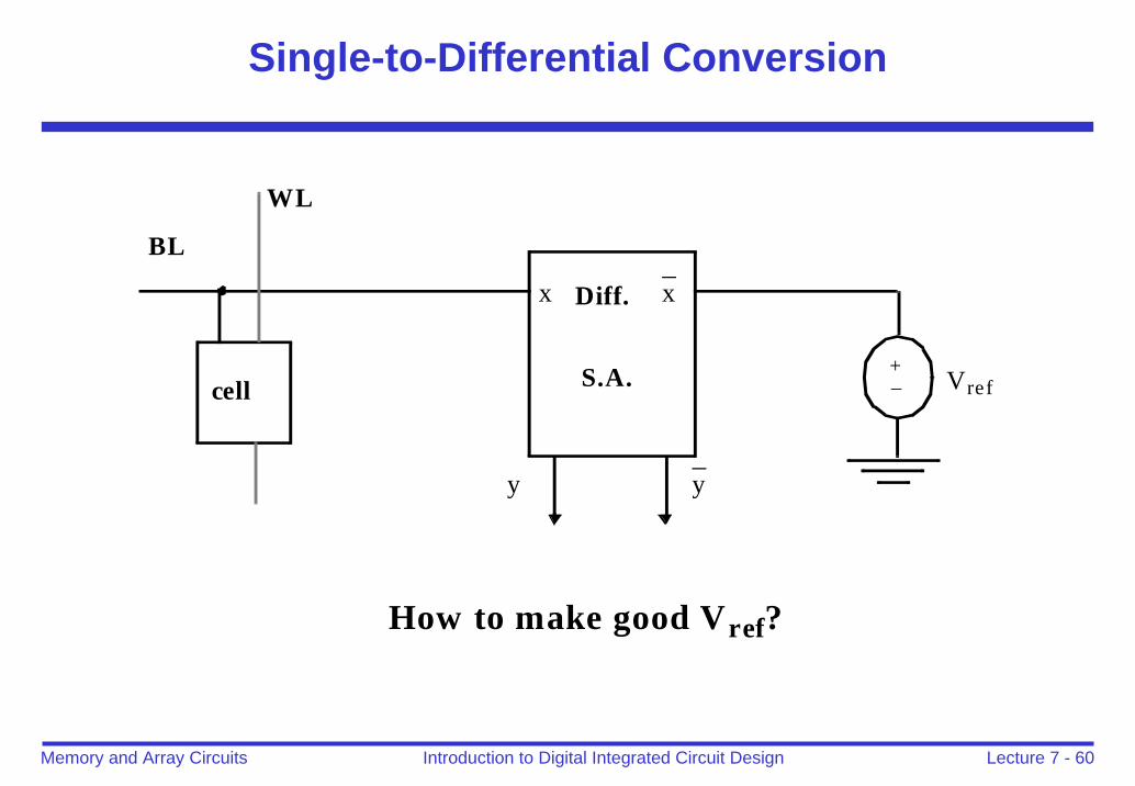
Single-to-Differential Conversion
Diff.
S.A.cell
BL
Vref+_
WL
x x
y y
How to make good Vref?
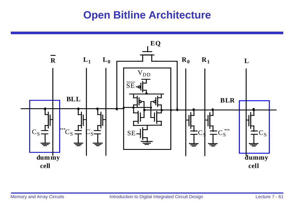
Lecture 7 - 61Introduction to Digital Integrated Circuit DesignMemory and Array Circuits
Open Bitline Architecture
VDD
SE
SE
CS CS CS
L
...CSCS...
CS
R
BLL BLR
L0L1 R0 R1
dummycell
dummycell
EQ
Lecture 7 - 62Introduction to Digital Integrated Circuit DesignMemory and Array Circuits
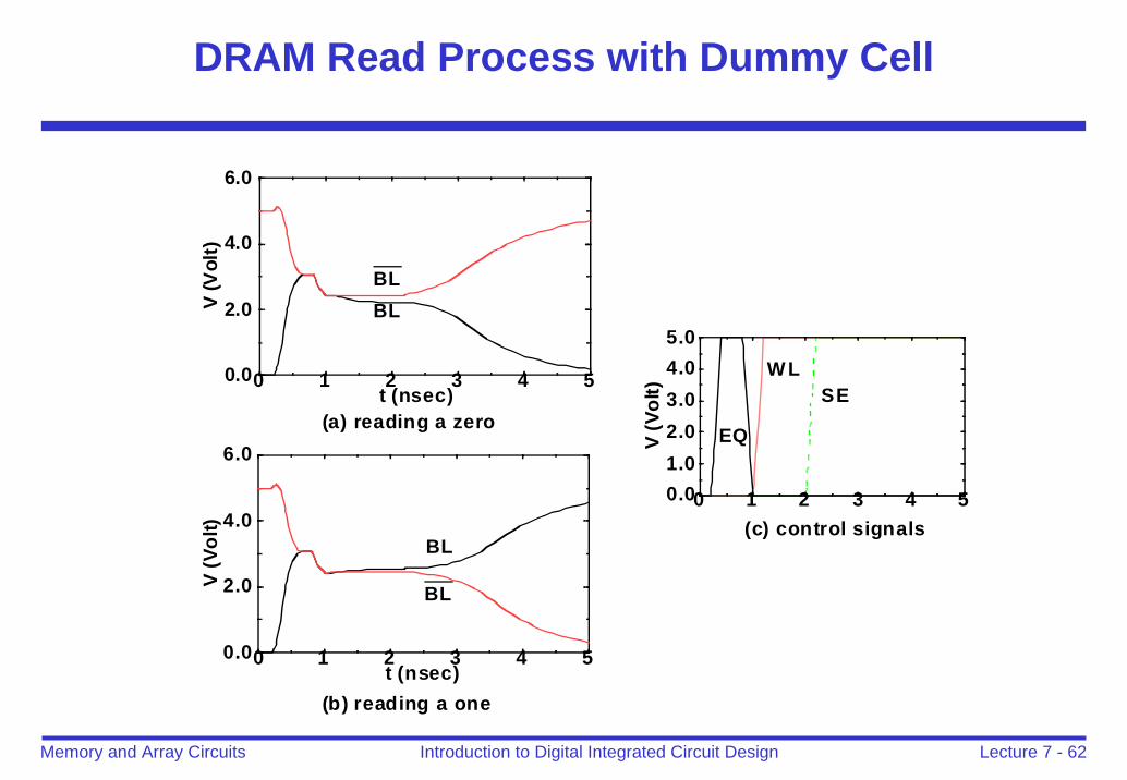
DRAM Read Process with Dummy Cell
0 1 2 3 4 5t (nsec)
0.0
2.0
4.0
6.0V
(Vol
t)
0 1 2 3 4 5t (nsec)
0.0
2.0
4.0
6.0
V (V
olt)
0 1 2 3 4 50.01.02.03.04.05.0
V (V
olt)
EQ
WLSE
BLBL
BL
BL
(a) reading a zero
(b) reading a one
(c) control signals
Lecture 7 - 63Introduction to Digital Integrated Circuit DesignMemory and Array Circuits
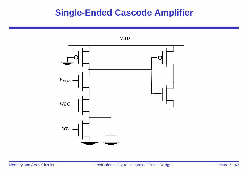
Single-Ended Cascode Amplifier
VDD
WL
WLC
Vcasc
Lecture 7 - 64Introduction to Digital Integrated Circuit DesignMemory and Array Circuits
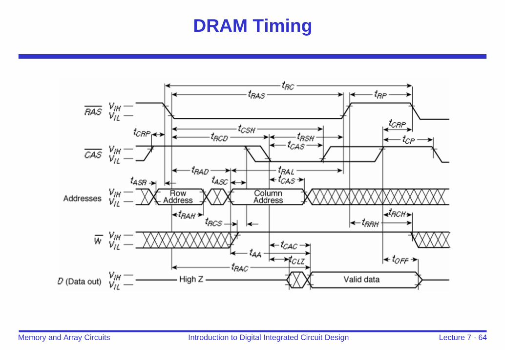
DRAM Timing
Lecture 7 - 65Introduction to Digital Integrated Circuit DesignMemory and Array Circuits
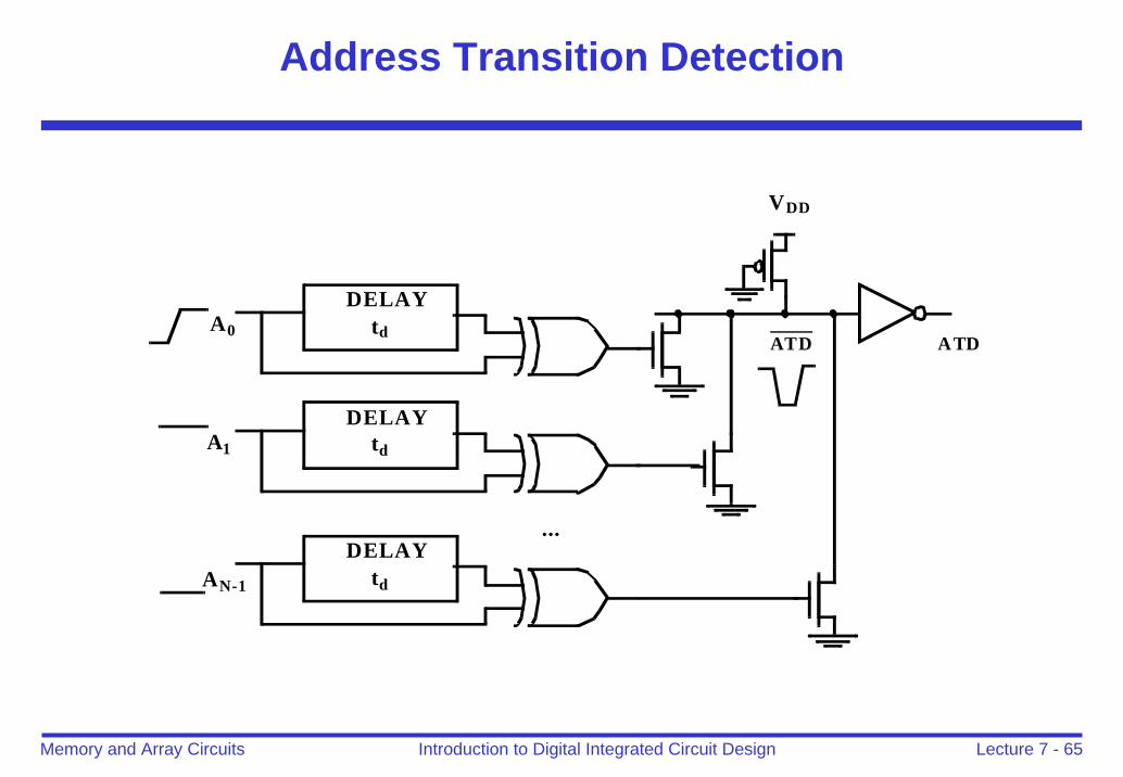
Address Transition Detection
DELAYtdA0
DELAYtd
DELAYtd
ATD
...
A1
AN-1
VDD
ATD
Lecture 7 - 66Introduction to Digital Integrated Circuit DesignMemory and Array Circuits
Outline
Memory classificationBasic building blocksROMNon Volatile Read Write MemoriesStatic RAM (SRAM)Dynamic RAM (DRAM)Memory peripheral circuitContent Addressable Memory (CAM)Serial access memoriesProgrammable Logic ArrayReliability and YieldMemory trends
Lecture 7 - 67Introduction to Digital Integrated Circuit DesignMemory and Array Circuits
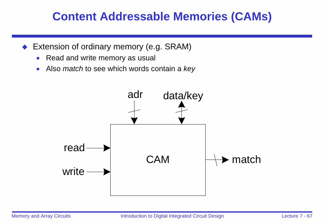
Content Addressable Memories (CAMs)
Extension of ordinary memory (e.g. SRAM)• Read and write memory as usual• Also match to see which words contain a key
CAM
adr data/key
matchread
write
Lecture 7 - 68Introduction to Digital Integrated Circuit DesignMemory and Array Circuits
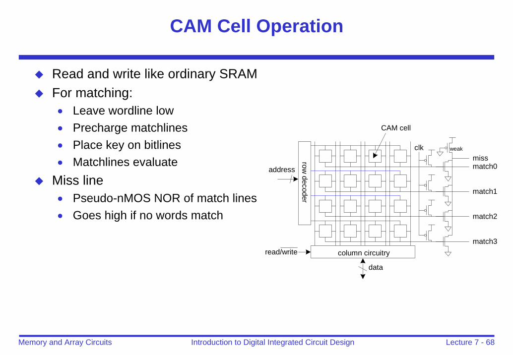
CAM Cell Operation
Read and write like ordinary SRAMFor matching:• Leave wordline low• Precharge matchlines• Place key on bitlines• Matchlines evaluate
Miss line• Pseudo-nMOS NOR of match lines• Goes high if no words match
row decoder
weak
missmatch0
match1
match2
match3
clk
column circuitry
CAM cell
address
data
read/write
Lecture 7 - 69Introduction to Digital Integrated Circuit DesignMemory and Array Circuits
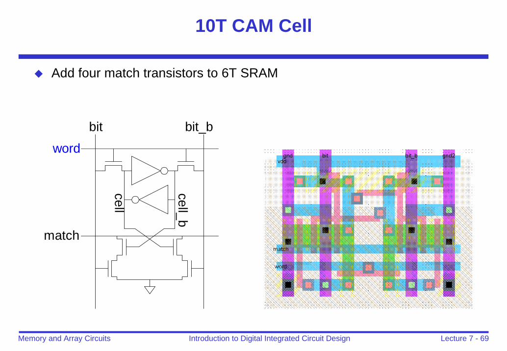
10T CAM Cell
Add four match transistors to 6T SRAM
bit bit_b
word
match
cell
cell_b
Lecture 7 - 70Introduction to Digital Integrated Circuit DesignMemory and Array Circuits
Outline
Memory classificationBasic building blocksROMNon Volatile Read Write MemoriesStatic RAM (SRAM)Dynamic RAM (DRAM)Memory peripheral circuitContent Addressable Memory (CAM)Serial access memoriesProgrammable Logic ArrayReliability and YieldMemory trends
Lecture 7 - 71Introduction to Digital Integrated Circuit DesignMemory and Array Circuits
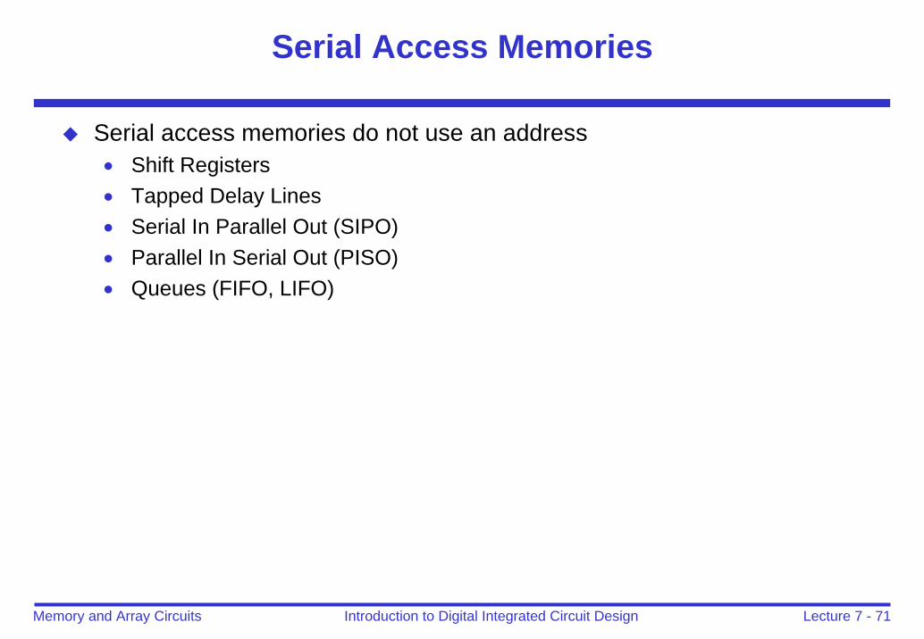
Serial Access Memories
Serial access memories do not use an address• Shift Registers• Tapped Delay Lines• Serial In Parallel Out (SIPO)• Parallel In Serial Out (PISO)• Queues (FIFO, LIFO)
Lecture 7 - 72Introduction to Digital Integrated Circuit DesignMemory and Array Circuits
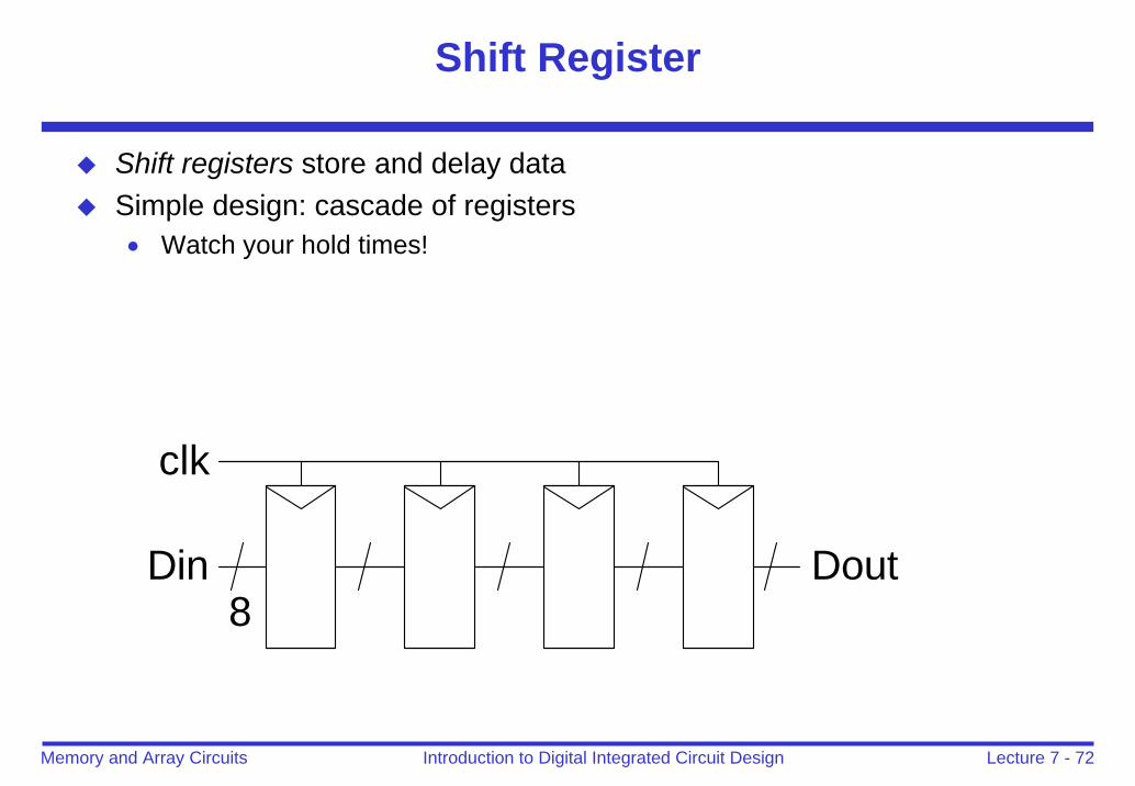
Shift Register
Shift registers store and delay dataSimple design: cascade of registers• Watch your hold times!
clk
Din Dout8
Lecture 7 - 73Introduction to Digital Integrated Circuit DesignMemory and Array Circuits
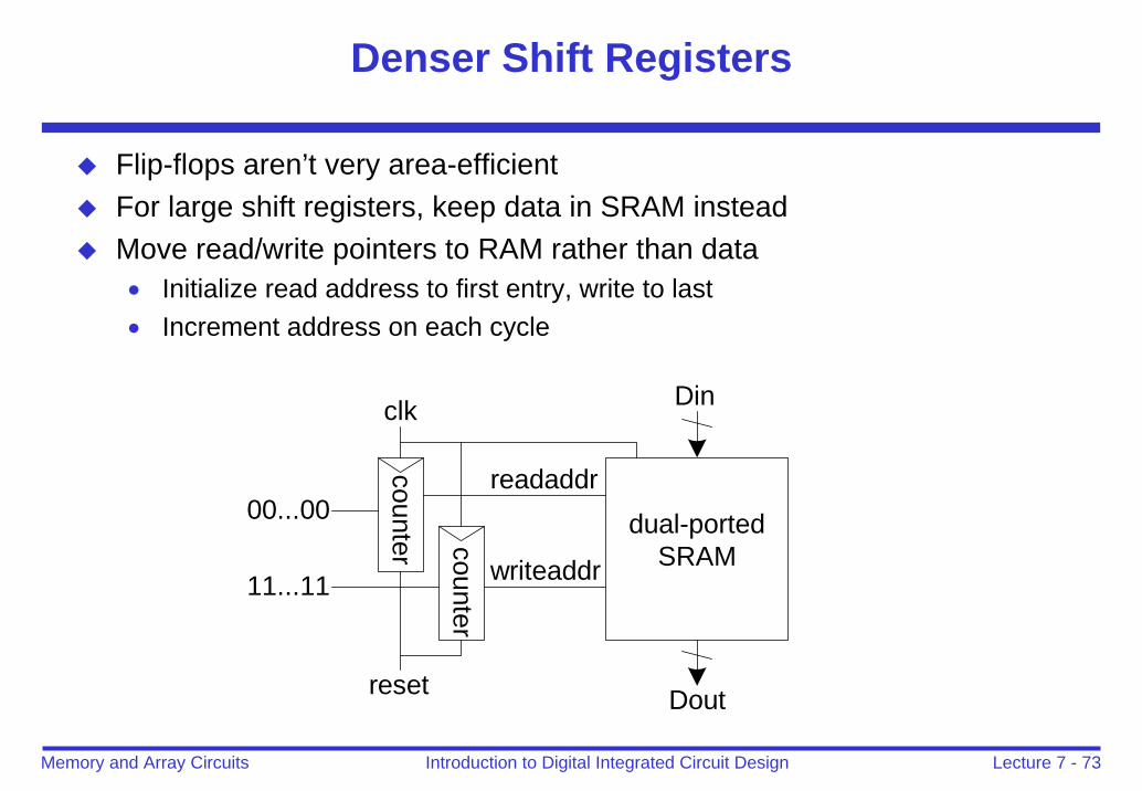
Denser Shift Registers
Flip-flops aren’t very area-efficientFor large shift registers, keep data in SRAM insteadMove read/write pointers to RAM rather than data• Initialize read address to first entry, write to last• Increment address on each cycle
Din
Dout
clk
counter counterreset
00...00
11...11
readaddr
writeaddr
dual-portedSRAM
Lecture 7 - 74Introduction to Digital Integrated Circuit DesignMemory and Array Circuits
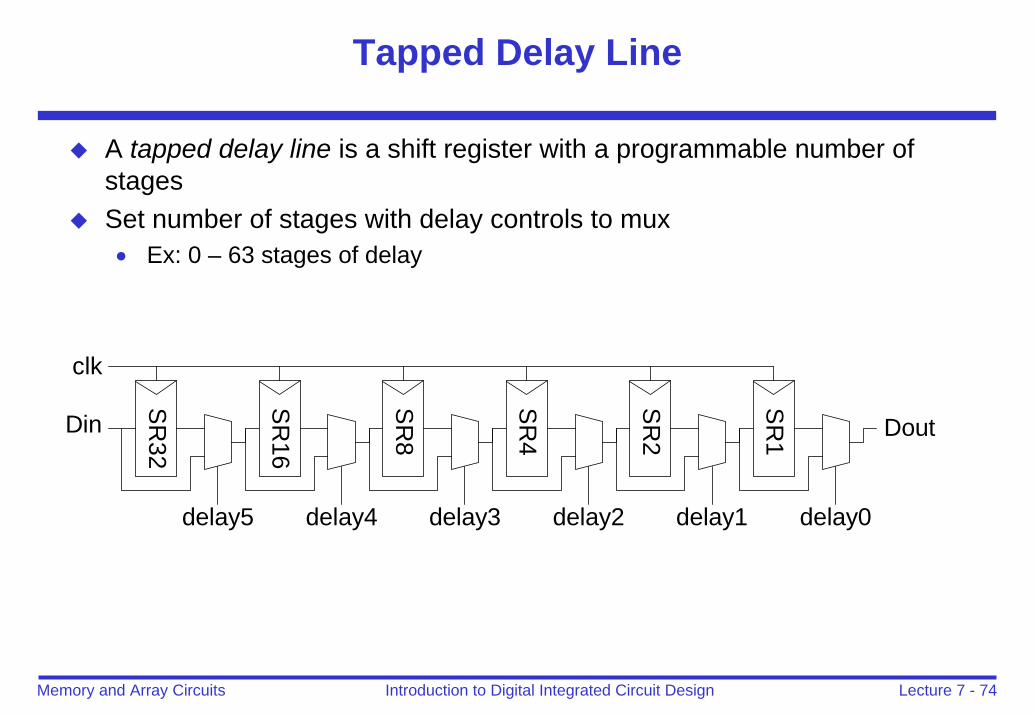
Tapped Delay Line
A tapped delay line is a shift register with a programmable number of stagesSet number of stages with delay controls to mux• Ex: 0 – 63 stages of delay
SR
32
clk
Din
delay5
SR
16
delay4
SR
8
delay3S
R4
delay2
SR
2
delay1
SR
1
delay0
Dout
Lecture 7 - 75Introduction to Digital Integrated Circuit DesignMemory and Array Circuits
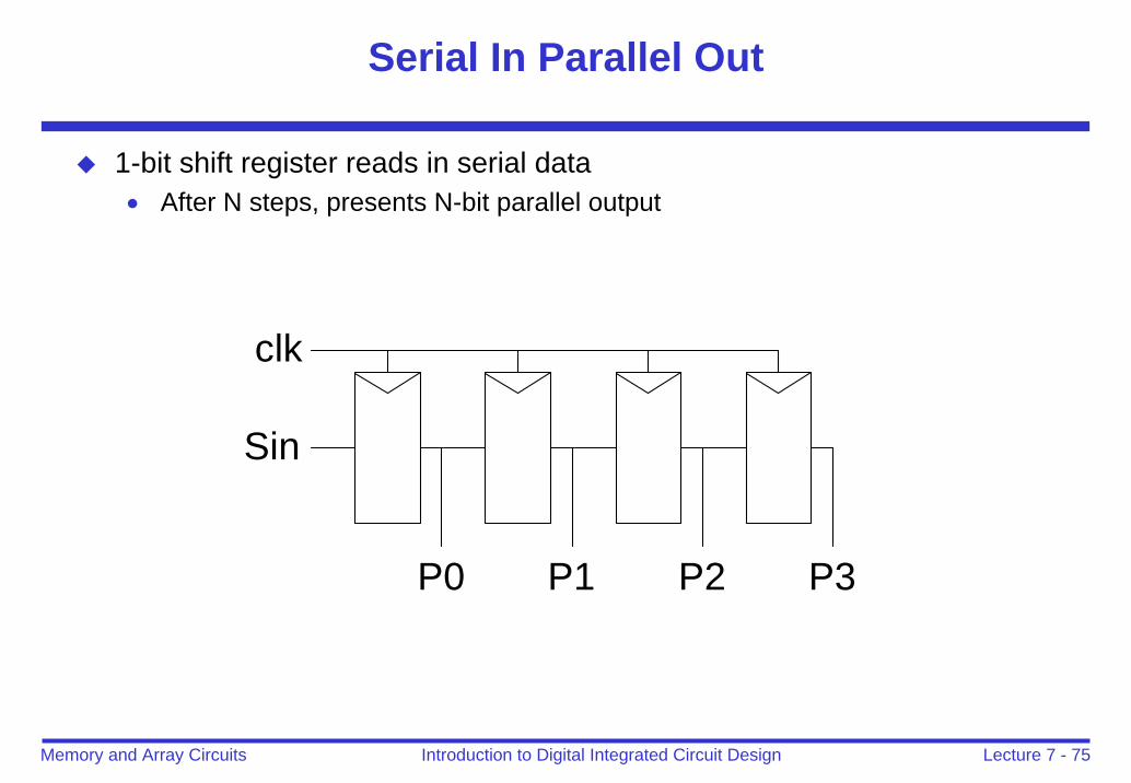
Serial In Parallel Out
1-bit shift register reads in serial data• After N steps, presents N-bit parallel output
clk
P0 P1 P2 P3
Sin
Lecture 7 - 76Introduction to Digital Integrated Circuit DesignMemory and Array Circuits
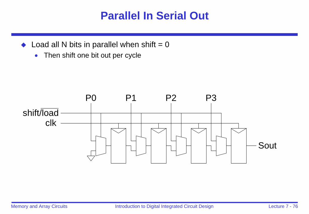
Parallel In Serial Out
Load all N bits in parallel when shift = 0• Then shift one bit out per cycle
clkshift/load
P0 P1 P2 P3
Sout
Lecture 7 - 77Introduction to Digital Integrated Circuit DesignMemory and Array Circuits
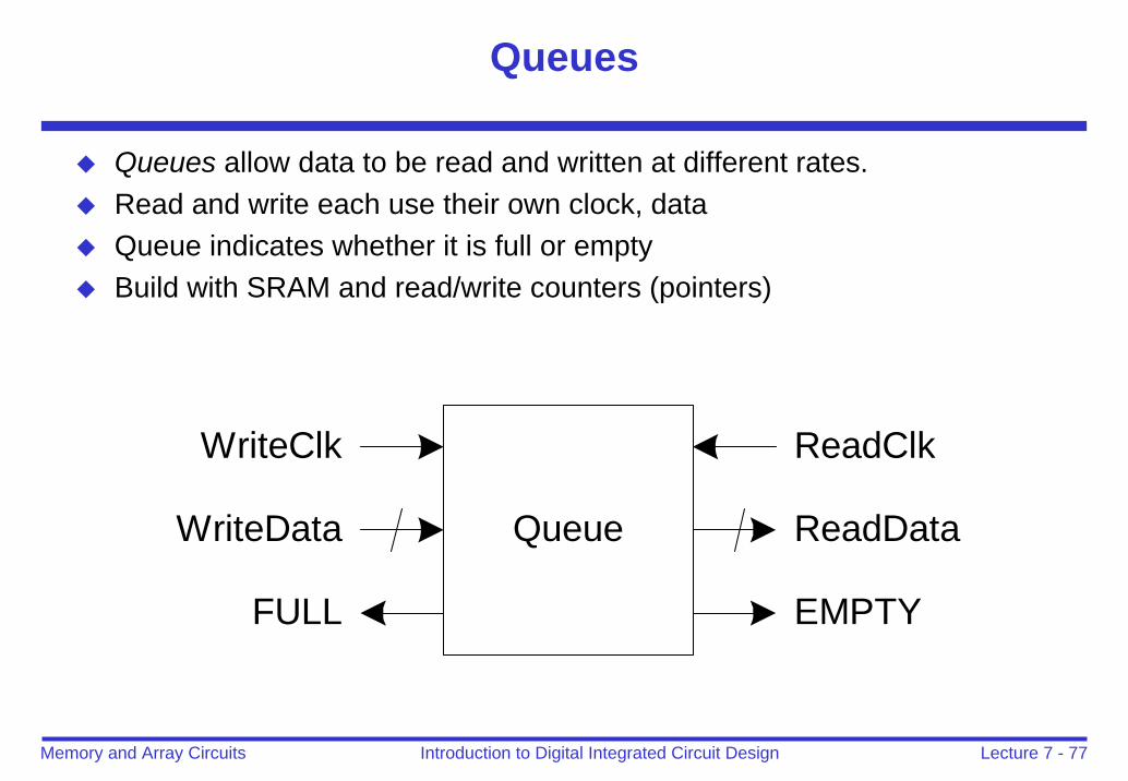
Queues
Queues allow data to be read and written at different rates.Read and write each use their own clock, dataQueue indicates whether it is full or emptyBuild with SRAM and read/write counters (pointers)
Queue
WriteClk
WriteData
FULL
ReadClk
ReadData
EMPTY
Lecture 7 - 78Introduction to Digital Integrated Circuit DesignMemory and Array Circuits
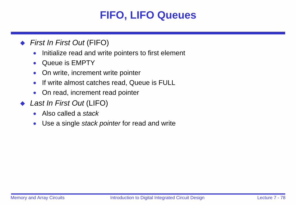
FIFO, LIFO Queues
First In First Out (FIFO)• Initialize read and write pointers to first element• Queue is EMPTY• On write, increment write pointer• If write almost catches read, Queue is FULL• On read, increment read pointer
Last In First Out (LIFO)• Also called a stack• Use a single stack pointer for read and write
Lecture 7 - 79Introduction to Digital Integrated Circuit DesignMemory and Array Circuits
Outline
Memory classificationBasic building blocksROMNon Volatile Read Write MemoriesStatic RAM (SRAM)Dynamic RAM (DRAM)Memory peripheral circuitContent Addressable Memory (CAM)Serial access memoriesProgrammable Logic ArraysReliability and YieldMemory trends
Lecture 7 - 80Introduction to Digital Integrated Circuit DesignMemory and Array Circuits
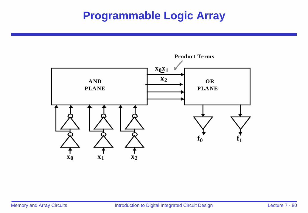
Programmable Logic Array
x0 x1 x2
f0 f1
A NDPLA NE
ORPLA NE
x0x1x2
Product Terms
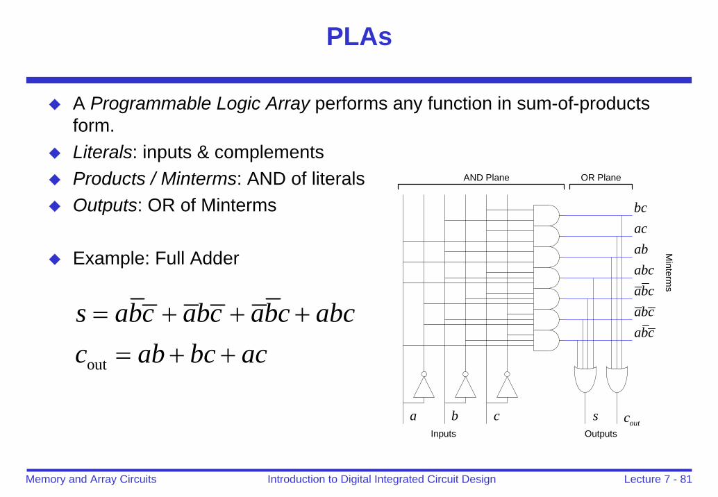
Lecture 7 - 81Introduction to Digital Integrated Circuit DesignMemory and Array Circuits
PLAs
A Programmable Logic Array performs any function in sum-of-products form.Literals: inputs & complementsProducts / Minterms: AND of literalsOutputs: OR of Minterms
Example: Full Adder
out
s abc abc abc abcc ab bc ac
= + + += + +
AND Plane OR Plane
abcabcabcabcab
bcac
sa b coutc
Minterm
s
Inputs Outputs
Lecture 7 - 82Introduction to Digital Integrated Circuit DesignMemory and Array Circuits
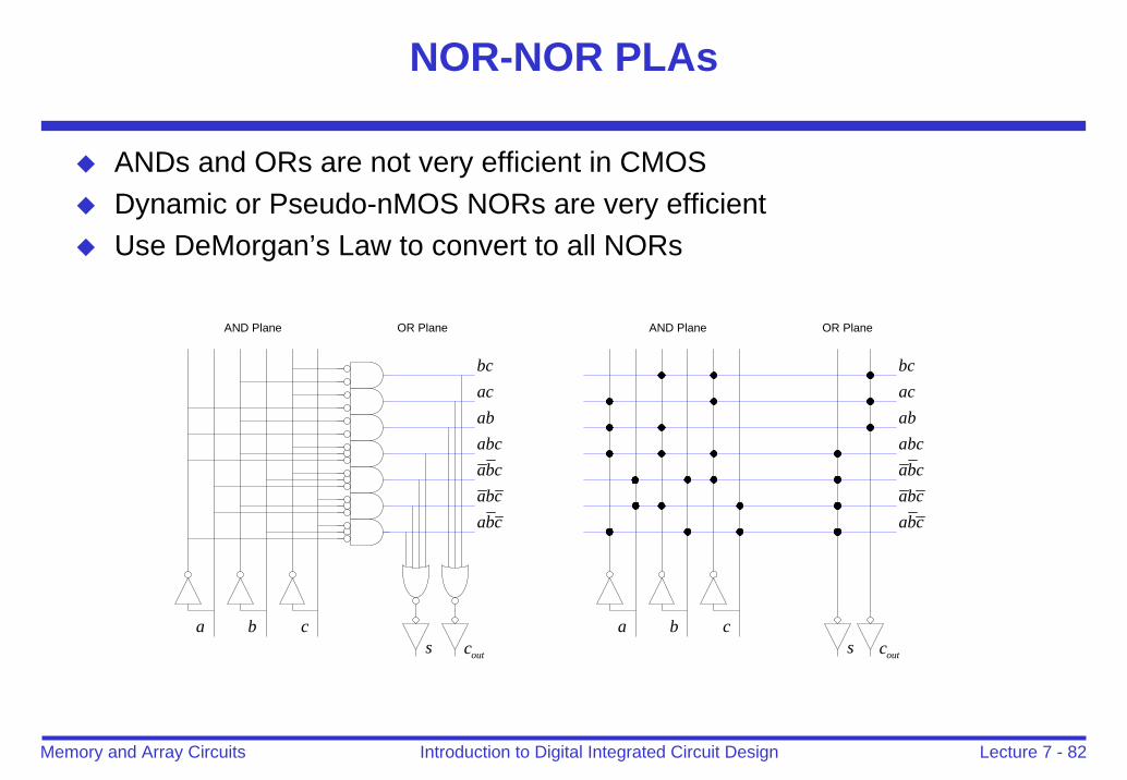
NOR-NOR PLAs
ANDs and ORs are not very efficient in CMOSDynamic or Pseudo-nMOS NORs are very efficientUse DeMorgan’s Law to convert to all NORs
AND Plane OR Plane
abcabcabcabcab
bcac
sa b c
outc
AND Plane OR Plane
abcabcabcabcab
bcac
sa b c
outc
Lecture 7 - 83Introduction to Digital Integrated Circuit DesignMemory and Array Circuits
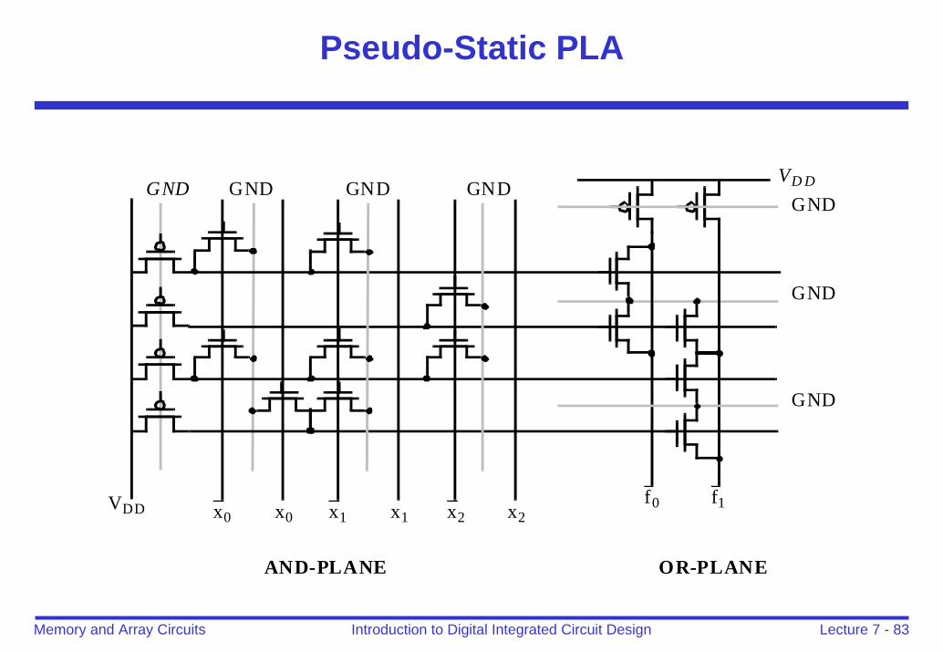
Pseudo-Static PLA
f0 f1
GND
GND
VD D
GND
x0 x0 x1 x1 x2 x2
GND GND GND GND
VDD
AND-PLANE OR-PLANE
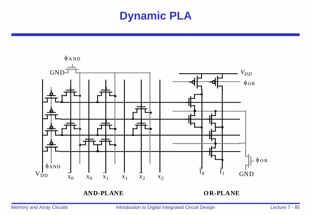
Lecture 7 - 84Introduction to Digital Integrated Circuit DesignMemory and Array Circuits
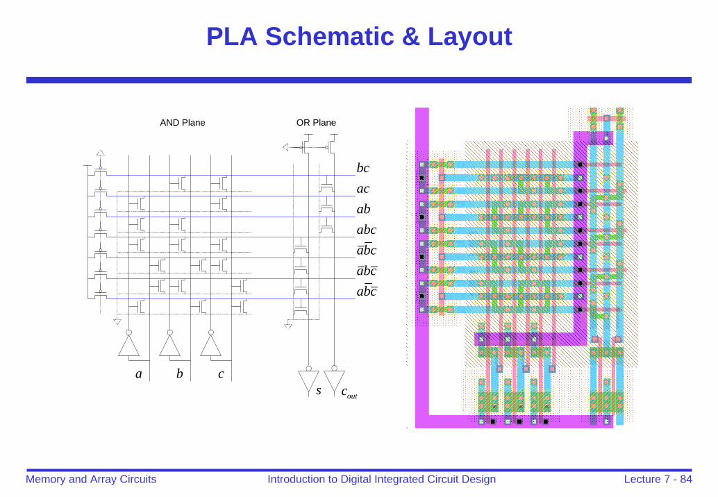
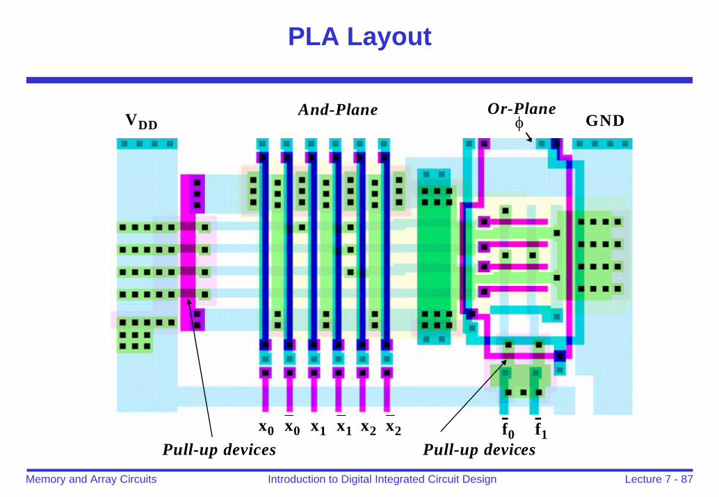
PLA Schematic & Layout
AND Plane OR Plane
abcabcabcabcab
bcac
sa b c
outc
Lecture 7 - 85Introduction to Digital Integrated Circuit DesignMemory and Array Circuits
Dynamic PLA
f0 f1 GND
VDD
φOR
x0 x0 x1 x1 x2 x2
GND
VDD
AND-PLANE OR-PLANE
φANDφO R
φA ND
Lecture 7 - 86Introduction to Digital Integrated Circuit DesignMemory and Array Circuits
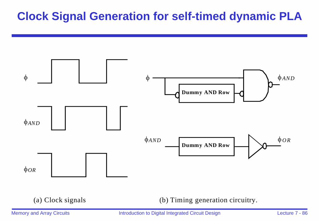
Clock Signal Generation for self-timed dynamic PLA
φ
φAND
φOR
φ φAND
Dummy AND Row
φANDDummy AND Row
φOR
(a) Clock signals (b) Timing generation circuitry.
Lecture 7 - 87Introduction to Digital Integrated Circuit DesignMemory and Array Circuits
PLA Layout
VDD GNDφAnd-Plane Or-Plane
f0 f1x0 x0 x1 x1 x2 x2Pull-up devices Pull-up devices
Lecture 7 - 88Introduction to Digital Integrated Circuit DesignMemory and Array Circuits
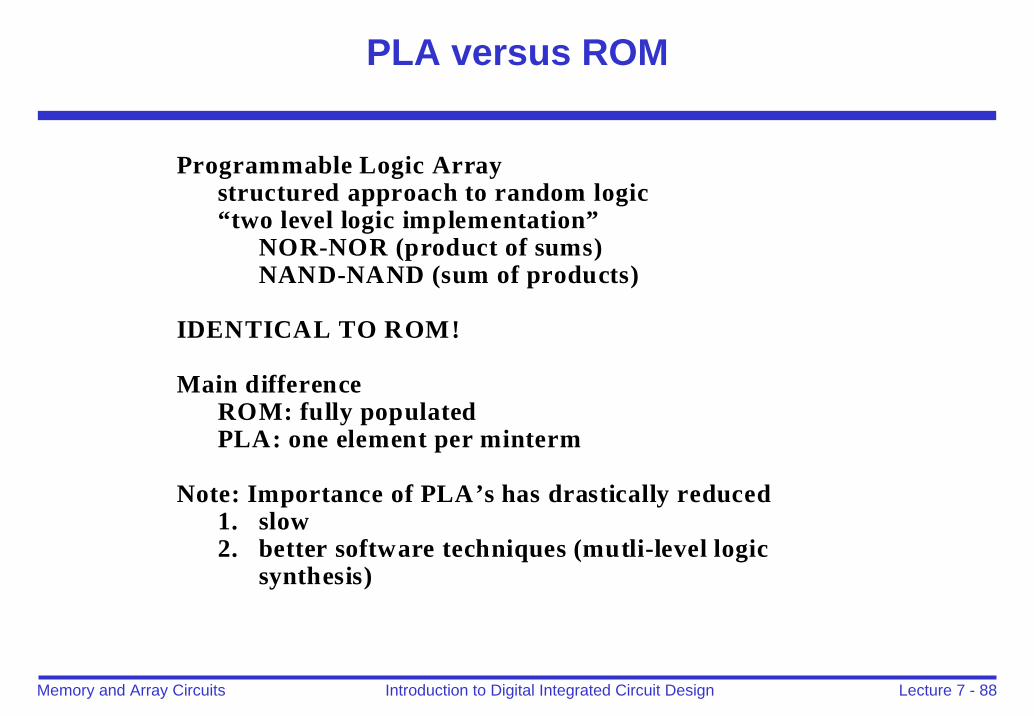
PLA versus ROM
Programmable Logic Arraystructured approach to random logic“two level logic implementation”
NOR-NOR (product of sums)NAND-NAND (sum of products)
IDENTICAL TO ROM!
Main differenceROM: fully populatedPLA: one element per minterm
Note: Importance of PLA’s has drastically reduced1. slow2. better software techniques (mutli-level logic
synthesis)
Lecture 7 - 89Introduction to Digital Integrated Circuit DesignMemory and Array Circuits
Outline
Memory classificationBasic building blocksROMNon Volatile Read Write MemoriesStatic RAM (SRAM)Dynamic RAM (DRAM)Memory peripheral circuitSerial access memoriesContent Addressable Memory (CAM)Programmable Logic ArrayReliability and YieldMemory trends
Lecture 7 - 90Introduction to Digital Integrated Circuit DesignMemory and Array Circuits
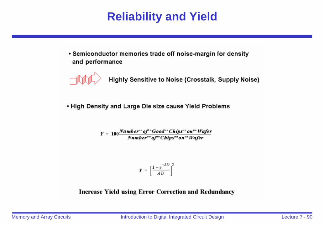
Reliability and Yield
Lecture 7 - 91Introduction to Digital Integrated Circuit DesignMemory and Array Circuits
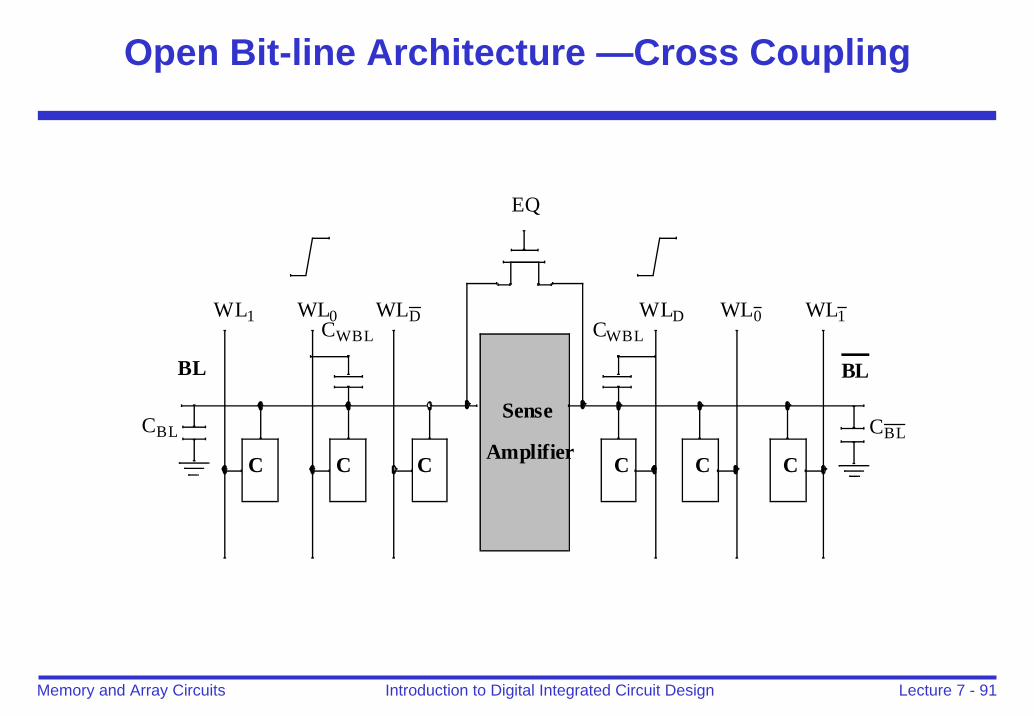
Open Bit-line Architecture —Cross Coupling
Sense
Amplifier C C CCCC
WL1 WL0 WLD WLD WL0 WL1
EQ
CWBLCWBL
CBL
BL
CBL
BL
Lecture 7 - 92Introduction to Digital Integrated Circuit DesignMemory and Array Circuits
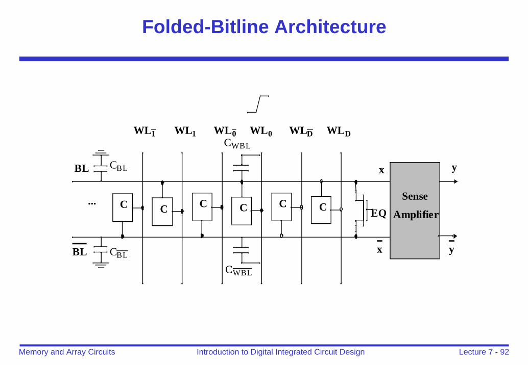
Folded-Bitline Architecture
BL
...
WLDWLD
BL
y
yx
x
WL0
CCCCCCEQ
Sense
Amplifier
WL0WL1WL1
CBL
CBL
CWBL
CWBL
Lecture 7 - 93Introduction to Digital Integrated Circuit DesignMemory and Array Circuits
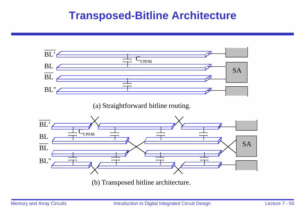
Transposed-Bitline Architecture
BLBL
BL’
BL"
SA
Ccross
SABLBL
BL’
BL"
Ccross
(a) Straightforward bitline routing.
(b) Transposed bitline architecture.
Lecture 7 - 94Introduction to Digital Integrated Circuit DesignMemory and Array Circuits
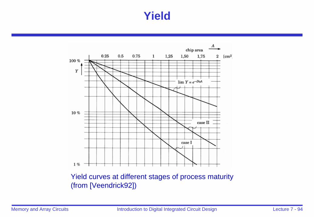
Yield
Yield curves at different stages of process maturity(from [Veendrick92])
Lecture 7 - 95Introduction to Digital Integrated Circuit DesignMemory and Array Circuits
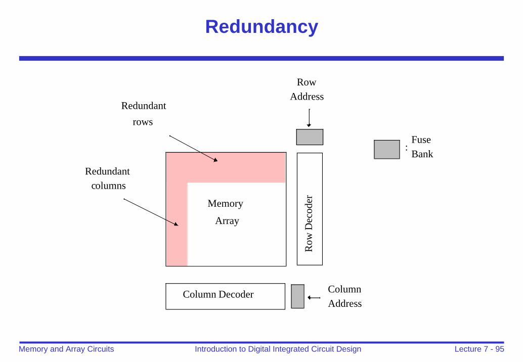
Redundancy
Memory
Array
Redundantcolumns
Redundantrows
Column DecoderR
ow D
ecod
er
RowAddress
ColumnAddress
FuseBank
:
Lecture 7 - 96Introduction to Digital Integrated Circuit DesignMemory and Array Circuits
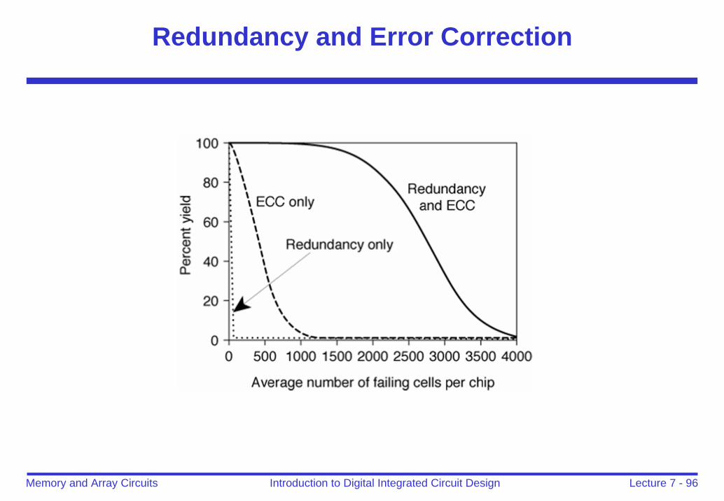
Redundancy and Error Correction
Lecture 7 - 97Introduction to Digital Integrated Circuit DesignMemory and Array Circuits
Outline
Memory classificationBasic building blocksROMNon Volatile Read Write MemoriesStatic RAM (SRAM)Dynamic RAM (DRAM)Memory peripheral circuitSerial access memoriesContent Addressable Memory (CAM)Programmable Logic ArrayReliability and YieldMemory trends
Lecture 7 - 98Introduction to Digital Integrated Circuit DesignMemory and Array Circuits
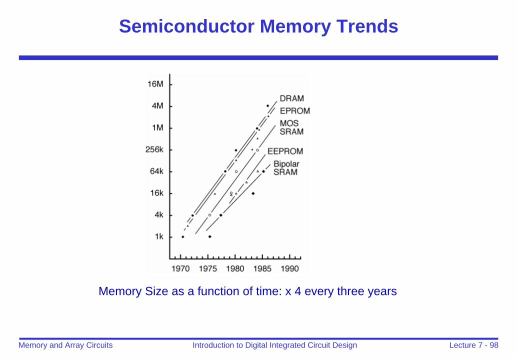
Semiconductor Memory Trends
Memory Size as a function of time: x 4 every three years
Lecture 7 - 99Introduction to Digital Integrated Circuit DesignMemory and Array Circuits
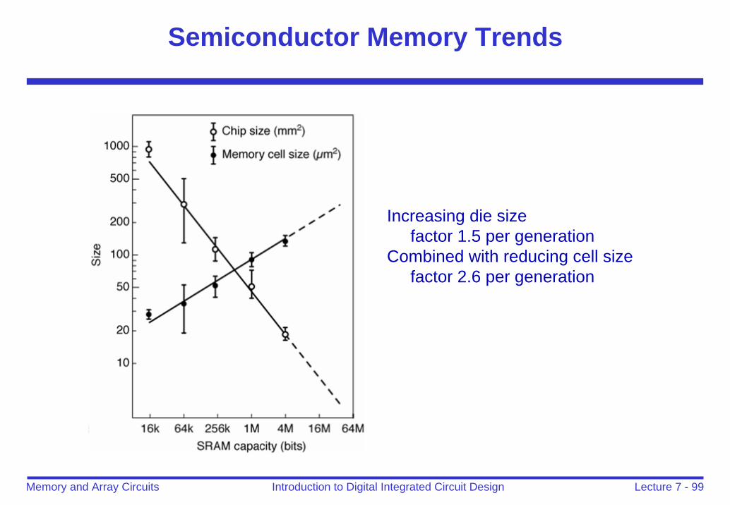
Semiconductor Memory Trends
Increasing die sizefactor 1.5 per generation
Combined with reducing cell sizefactor 2.6 per generation
Lecture 7 - 100Introduction to Digital Integrated Circuit DesignMemory and Array Circuits
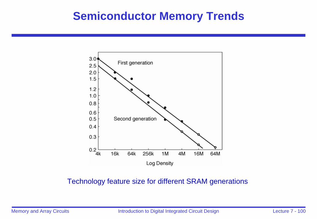
Semiconductor Memory Trends
Technology feature size for different SRAM generations


![[Array, Array, Array, Array, Array, Array, Array, Array, Array, Array, Array, Array]](https://img.pdfslide.net/doc/110x75/56816460550346895dd63b8b/array-array-array-array-array-array-array-array-array-array-array.jpg)

