Embed Size (px)
Citation preview

Lecture 8
ANNOUNCEMENTS• A summary of frequently misunderstood/missed concepts is• A summary of frequently misunderstood/missed concepts is
now posted on the class website, and will be updated regularly.• Graded HW assignments can be picked up in lab (353 Cory).
OUTLINE
Please indicate your lab section on your HW assignments!
OUTLINE• BJT Amplifiers (cont’d)
– Common‐emitter topology– CE stage with emitter degeneration– Impact of Early effect (ro)
EE105 Fall 2007 Lecture 8, Slide 1 Prof. Liu, UC Berkeley
Reading: Finish Chapter 5.3.1

Emitter Degeneration• By inserting a resistor in series with the emitter, we “degenerate” the CE stage. g g
• This topology will decrease the gain of the amplifier but improve other aspects, such as linearity, and input
dimpedance.
EE105 Fall 2007 Lecture 8, Slide 2 Prof. Liu, UC Berkeley

Small‐Signal Analysis
• The gain of a degenerated CE stage = the total load resistance seen at the collector divided by 1/g plusresistance seen at the collector divided by 1/gm plus the total resistance placed in series with the emitter.
RRg −−
Em
C
Em
Cmv
Rg
RRgRgA
+=
+= 11
mg
EE105 Fall 2007 Lecture 8, Slide 3 Prof. Liu, UC Berkeley

Emitter Degeneration Example 1
Note that the input impedance of Q2 is in parallel with RE.
2||1πrR
RAE
Cv
+−=
EE105 Fall 2007 Lecture 8, Slide 4 Prof. Liu, UC Berkeley
21
|| πg Em

Emitter Degeneration Example 2
Note that the input impedance of Q2 is in parallel with RC.
E
Cv
R
rRA+
−= 2
1|| π
EE105 Fall 2007 Lecture 8, Slide 5 Prof. Liu, UC Berkeley
Emg 1

Input Impedance of Degenerated CE Stage
• With emitter degeneration, the input impedance is increased from r to r + (β+1)R ― a desirable effectincreased from rπ to rπ + (β+1)RE a desirable effect.
A
iRiV
)1()( ∞=
β
Ex
in
xExx
RrvR
iRirv
)1(
)1(
++=≡
++=
β
β
π
π
EE105 Fall 2007 Lecture 8, Slide 6 Prof. Liu, UC Berkeley
Ex
in i)(βπ

Output Impedance of Degenerated CE Stage
• Emitter degeneration does not alter the output impedance if the Early effect is negligibleimpedance, if the Early effect is negligible.
A
Rv
V
⇒⎞
⎜⎜⎛
++
∞=
00
)(
π
x
Emin
RvR
vRvgr
vv =⇒⎠
⎜⎜⎝
++== 00 πππ
ππ
EE105 Fall 2007 Lecture 8, Slide 7 Prof. Liu, UC Berkeley
Cx
xout R
iR =≡

Degenerated CE Stage as a “Black Box”
AV ∞= )(
E
inmout Rgr
vgi++
= − )(1 1
• If gmRE >> 1, Gm is more linear.mout
m
Em
RgiG
Rgr
+≈≡
++
1
)(1 π
EE105 Fall 2007 Lecture 8, Slide 8 Prof. Liu, UC Berkeley
gm E , mEmin Rgv +1

Degenerated CE Stage with Base Resistance
)( ∞=AV
.=
βA
out
in
A
in
out
vv
vv
vv
)1( +++−
=β
β
π BE
C
in
out
RRrR
vv
1++
−≈
BE
Cv RR
RA
EE105 Fall 2007 Lecture 8, Slide 9 Prof. Liu, UC Berkeley
1+++βE
m
Rg

Degenerated CE Stage: Input/Output ImpedancesInput/Output Impedances
• Rin1 is more important in practice, because RB is often the output impedance of the previous stagethe output impedance of the previous stage.
AV ∞= )(
Ein
A
RRRRrR+++
++=)1(
)1(1
ββπ
Cout
EBin
RRRrRR
=+++= )1(2 βπ
EE105 Fall 2007 Lecture 8, Slide 10 Prof. Liu, UC Berkeley

Emitter Degeneration Example 3
2
1
1)||(RR
RRAB
Cv
++
−=
2
2
)1(1RRrR
g
Bin
m
+++=+
ββ
π
EE105 Fall 2007 Lecture 8, Slide 11 Prof. Liu, UC Berkeley
1|| RRR Cout =

Output Impedance of Degenerated CE Stage with VA<∞with VA
• Emitter degeneration boosts the output impedance.– This improves the gain of the amplifier and makes theThis improves the gain of the amplifier and makes the circuit a better current source.
[ ])||)(1(
||)||(1
π
ππ
rRrgrRrRrrRgR
EOmOout
EOEmout
++=++=
EE105 Fall 2007 Lecture 8, Slide 12 Prof. Liu, UC Berkeley
[ ])||(1 π
π
rRgrR EmOout
EOmOout
+≈

Two Special Cases
Stage with explicit depiction of ro:
OmOoutE rrgrRrR )1( : )1 ≈+≈>> ππ β
OEE rRgRrR )1(:)2 +≈<<
EE105 Fall 2007 Lecture 8, Slide 13 Prof. Liu, UC Berkeley
OEmoutE rRgRrR )1( :)2 +≈<< π

Analysis by Inspection• This seemingly complicated circuit can be greatly simplified by first recognizing that the capacitor creates an AC short to ground, and gradually transforming the circuit to a known topology.
[ ][ ]EE105 Fall 2007 Lecture 8, Slide 14 Prof. Liu, UC Berkeley
[ ] 12 ||)||(1 RrrRgR Omout π+=[ ] Omout rrRgR )||(1 21 π+=11 || outout RRR =

Example: Degeneration by Another BJT
[ ] 1121 )||(1 OOmout rrrgR π+=
• Called a “cascode”, this circuit offers many advantages
EE105 Fall 2007 Lecture 8, Slide 15 Prof. Liu, UC Berkeley
, y gthat we will study later...

Bad Input Connection
• Since the microphone has a very low resistance (connecting the base of Q1 to ground), it attenuates ( g 1 g )the base voltage and renders Q1 with a very small bias current.
EE105 Fall 2007 Lecture 8, Slide 16 Prof. Liu, UC Berkeley

Use of Coupling Capacitor
• A capacitor is used to isolate the DC bias network from the microphone and to short (or “couple”) thefrom the microphone , and to short (or couple ) the microphone to the amplifier at higher frequencies.
EE105 Fall 2007 Lecture 8, Slide 17 Prof. Liu, UC Berkeley

DC and AC Analysis• The coupling capacitor is replaced with an open circuit for DC analysis, and then replaced with a shortcircuit for DC analysis, and then replaced with a short circuit for AC analysis.
Bin
OCmv
RrRrRgA
||)||(
=−=
π
OCout rRR ||=
EE105 Fall 2007 Lecture 8, Slide 18 Prof. Liu, UC Berkeley
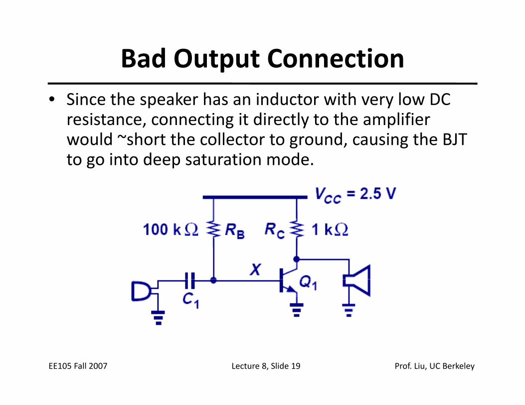
Bad Output Connection• Since the speaker has an inductor with very low DC resistance, connecting it directly to the amplifier , g y pwould ~short the collector to ground, causing the BJT to go into deep saturation mode.
EE105 Fall 2007 Lecture 8, Slide 19 Prof. Liu, UC Berkeley

Use of Coupling Capacitor at Output• The AC coupling indeed allows for correct biasing. However due to the speaker’s small inputHowever, due to the speaker s small input impedance, the overall gain drops considerably.
EE105 Fall 2007 Lecture 8, Slide 20 Prof. Liu, UC Berkeley

CE Stage with Voltage‐Divider Biasing
OCmv rRgA )||(−=
OCout
in
rRRRRrR
|||||| 21
== π
EE105 Fall 2007 Lecture 8, Slide 21 Prof. Liu, UC Berkeley

CE Stage with Robust Biasing
∞=V ∞AV
)( ∞=AVC
v
R
RA+
−= 1
)( ∞AV
[ ]Ein
Em
RRRrR
Rg
++=
+
21 ||||)1(βπ
EE105 Fall 2007 Lecture 8, Slide 22 Prof. Liu, UC BerkeleyCout RR =

Elimination of Emitter Degeneration for AC Signalsfor AC Signals
• The capacitor C2 shorts out RE at higher frequencies to eliminate the emitter degenerationto eliminate the emitter degeneration.
)( ∞=AV
i
Cmv
RRrRRgA
=−=
21 ||||
)( A
Cout
in
RRRRrR
=21 ||||π
EE105 Fall 2007 Lecture 8, Slide 23 Prof. Liu, UC Berkeley

Complete CE Stage
ss
LCv RRR
RRRRRR
RRA+
⋅++
−=
21
21
21 ||||
||||1||
EE105 Fall 2007 Lecture 8, Slide 24 Prof. Liu, UC Berkeley
ssE
m
Rg +
++ 2121 ||1β

Summary of CE Concepts
EE105 Fall 2007 Lecture 8, Slide 25 Prof. Liu, UC Berkeley