Embed Size (px)
Citation preview
Lecture: Silicon Photonics Waveguides
Prepared by Prof. Graham T. Reed,G. Mashanovich, M. Milosevic, and F. Gardes
University of Surrey, Guildford, UK
Waveguide materialsPlanar waveguidesRib and ridge waveguidesStrip waveguidesLossesPolarisation issuesEffect of stress
Contents
Silicon Photonics –PhD course prepared within FP7-224312 Helios project
Waveguide materialsPlanar waveguidesRib and ridge waveguidesStrip waveguidesLossesPolarisation issuesEffect of stress

Materials – Si and Ge
[Palik E D 1985 Handbook of Optical Constants of Solids vol 1 (New York: Academic)]
Refractive index and absorption loss of Si as a function of wavelength
Absorption coefficient of Ge as a function of wavenumber
[Hawkins G J 1998 Spectral characteristics of infrared optical materials and filters PhD Thesis Department of Cybernetics, University of Reading, UK]
Si3N4: 1.2 – 6.7 μm
Al2O3: 1.2 – 4.4 μm
(1.2 - 8 μm) + (24 – 200 μm)
(1.9 – 16.8 μm) + (140 – 200 μm)
Silicon Photonics –PhD course prepared within FP7-224312 Helios project
Materials – SiO2
[Palik E D 1985 Handbook of Optical Constants of Solids vol 1 (New York: Academic)]
Refractive index and absorption loss of SiO2 as a function of wavelength
[R. Soref et al, J. Opt. A: Pure Appl. Opt, 8 (840) 2006]
Absorption loss of SiO2 as a function of wavelength (2-5 μm)
Silicon Photonics –PhD course prepared within FP7-224312 Helios project
Waveguide materialsPlanar waveguidesRib and ridge waveguidesStrip waveguidesLossesPolarisation issuesEffect of stress
Silicon Photonics –PhD course prepared within FP7-224312 Helios project

n2
n1
2211 sinnsinn θ=θ
θ1
θ2n2
n1
Ei Er
Et
Light rays refracted and reflected at the interface of two media
θ1
θc
The Ray Optics Approach to Describing Planar Waveguides
Silicon Photonics –PhD course prepared within FP7-224312 Helios project
n1
n2
211 sin nn =θ
1
2sinnn
c =θ
Total internal reflection at two interfaces demonstrating the concept of a waveguide
Silicon Photonics –PhD course prepared within FP7-224312 Helios project

Reflection Coefficients
ir ErE .=
where ‘r’ is a complex reflection coefficient, which is polarisation dependant
The Transverse Electric (TE) condition is defined as the condition when the
electric fields of the waves are perpendicular to the plane of incidence.
Correspondingly, the Transverse Magnetic (TM) condition occurs when the magnetic fields are perpendicular to the plane of incidence.
n2
n1
Ei Er
Et
Circles indicate that the electric fields are vertical (i.e. coming out of screen)Orientation of electric fields for TE incidence at the interface between 2 media.
interface
Silicon Photonics –PhD course prepared within FP7-224312 Helios project
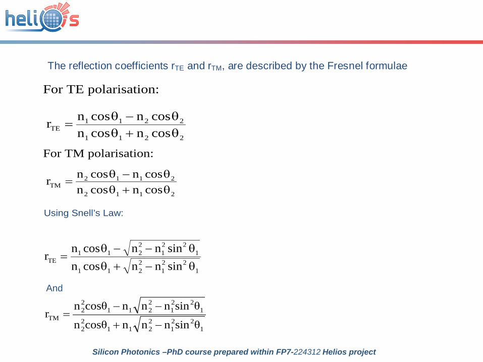
The reflection coefficients rTE and rTM, are described by the Fresnel formulae
For TE polarisation:
2211
2211TE cosncosn
cosncosnrθ+θθ−θ
=
For TM polarisation:
2112
2112TM cosncosn
cosncosnrθ+θθ−θ
=
Using Snell’s Law:
122
12211
122
12211
TE sinnncosnsinnncosn
rθ−+θθ−−θ
=
And
122
12211
22
122
12211
22
TMθsinnnncosθn
θsinnnncosθnr
−+
−−=
Silicon Photonics –PhD course prepared within FP7-224312 Helios project
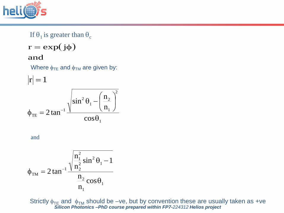
If θ1 is greater than θc
( )and
jexpr φ=
1r =Where φTE and φTM are given by:
and
1
2
1
21
2
1TE cos
nnsin
tan2θ
−θ
=φ −
11
2
12
22
21
1TM
cosnn
1sinnn
tan2θ
−θ=φ −
Strictly φTE and φTM should be –ve, but by convention these are usually taken as +veSilicon Photonics –PhD course prepared within FP7-224312 Helios project
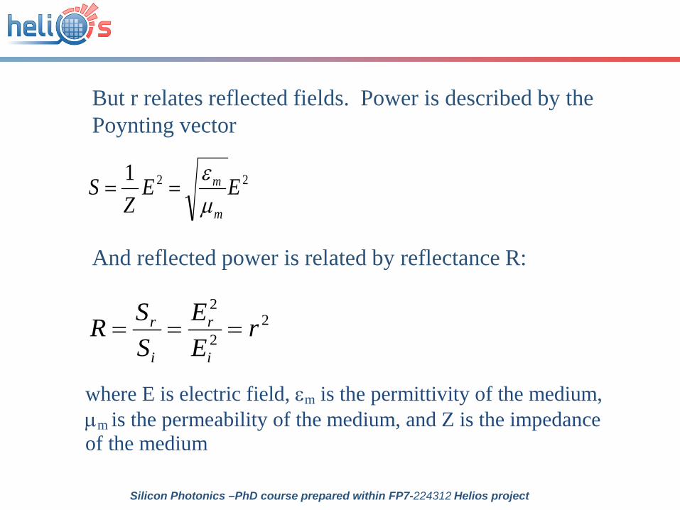
But r relates reflected fields. Power is described by the Poynting vector
221 EEZ
Sm
m
µε
==
And reflected power is related by reflectance R:
22
2
rEE
SSR
i
r
i
r ===
where E is electric field, εm is the permittivity of the medium, µm is the permeability of the medium, and Z is the impedance of the medium
Silicon Photonics –PhD course prepared within FP7-224312 Helios project
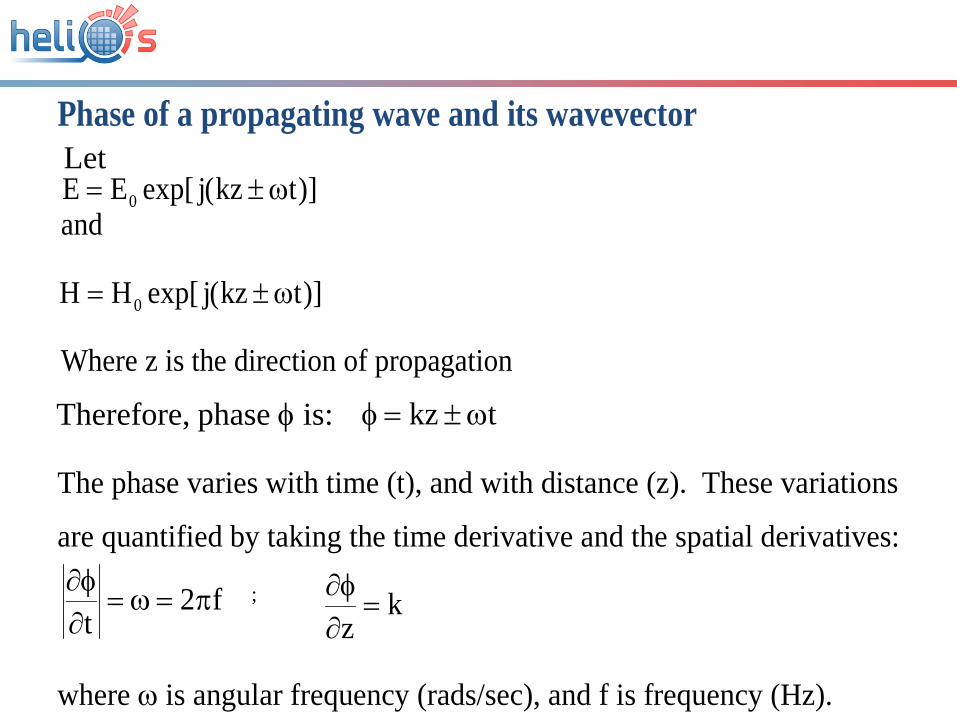
Phase of a propagating wave and its wavevector Let
and
Where z is the direction of propagation
)]tkz(jexp[EE 0 ω±=
)]tkz(jexp[HH 0 ω±=
Therefore, phase φ is: tkz ω±=φ
The phase varies with time (t), and with distance (z). These variations
are quantified by taking the time derivative and the spatial derivatives:
;
where ω is angular frequency (rads/sec), and f is frequency (Hz).
f2t
π=ω=∂φ∂
kz=
∂φ∂
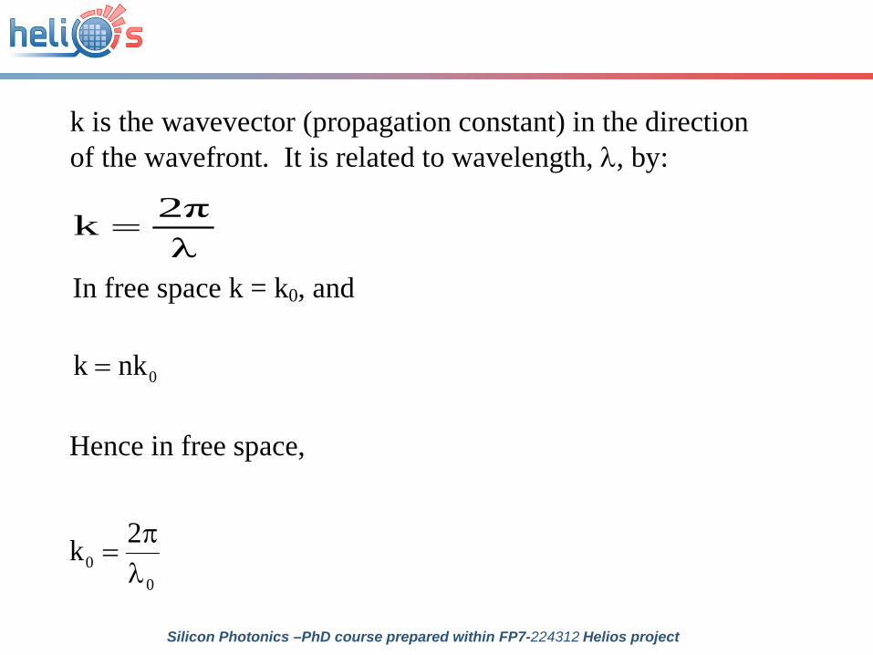
k is the wavevector (propagation constant) in the direction of the wavefront. It is related to wavelength, λ, by:
λ2πk =
In free space k = k0, and
Hence in free space,
0nkk =
00
2kλπ
=
Silicon Photonics –PhD course prepared within FP7-224312 Helios project

Modes of a planar waveguide
The wavevector in a planar waveguide
n1
n2
n3
y x z
h k0n1
We can decompose the wavevector k, into two components, in the y and z directions.
θ1k=n1k0
kz= n1k0sinθ1
ky= n1k0cosθ1
The relationship between propagation constants in the y, z, and wavenormal directions
Silicon Photonics –PhD course prepared within FP7-224312 Helios project
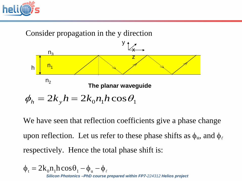
The planar waveguide
n1
n2
n3
y x z
h
Consider propagation in the y direction
110 cos22 θφ hnkhkyh ==
We have seen that reflection coefficients give a phase change
upon reflection. Let us refer to these phase shifts as φu, and φ
respectively. Hence the total phase shift is:
φ−φ−θ=φ u110t coshnk2
Silicon Photonics –PhD course prepared within FP7-224312 Helios project

For self this total phase shift must be a multiple of 2π,
hence:
π=φ−φ−θ m2coshnk2 u110
Thus light propagates in discrete modes described by the polarisation and the mode number.
E.g. TE0, TE1, TM0, etc
Each mode will have a unique propagation constant in the y and z directions
The number of modes is limited by satisfaction of the requirements of total internal reflection.
Silicon Photonics –PhD course prepared within FP7-224312 Helios project
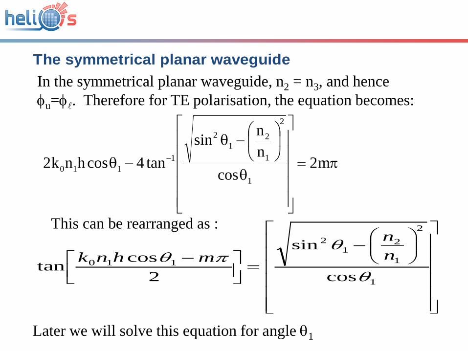
The symmetrical planar waveguide In the symmetrical planar waveguide, n2 = n3, and hence φu=φ. Therefore for TE polarisation, the equation becomes:
This can be rearranged as :
π=
θ
−θ
−θ − m2cos
nnsin
tan4coshnk21
2
1
21
2
1110
−
=
−
1
2
1
21
2
110
cos
sin
2costan
θ
θπθ n
nmhnk
Later we will solve this equation for angle θ1
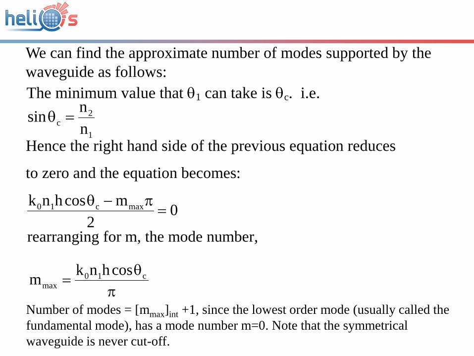
We can find the approximate number of modes supported by the waveguide as follows:The minimum value that θ1 can take is θc. i.e.
1
2c n
nsin =θ
Hence the right hand side of the previous equation reduces
to zero and the equation becomes:
0
2mcoshnk maxc10 =
π−θ
rearranging for m, the mode number,
πθ
= c10max
coshnkm
Number of modes = [mmax]int +1, since the lowest order mode (usually called the fundamental mode), has a mode number m=0. Note that the symmetrical waveguide is never cut-off.
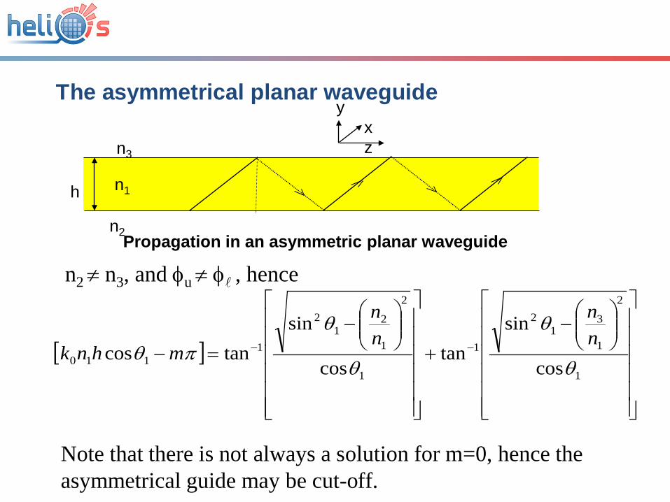
The asymmetrical planar waveguide
n2 ≠ n3, and φu ≠ φ , hence Propagation in an asymmetric planar waveguide
n1
n2
n3
y x z
h
[ ]
−
+
−
=− −−
1
2
1
31
2
1
1
2
1
21
2
1110 cos
sintan
cos
sintancos
θ
θ
θ
θπθ
nn
nn
mhnk
Note that there is not always a solution for m=0, hence the asymmetrical guide may be cut-off.
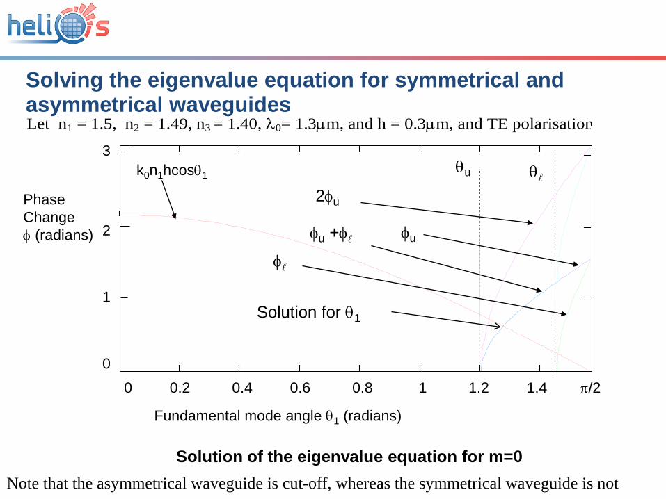
Solving the eigenvalue equation for symmetrical and asymmetrical waveguides Let n1 = 1.5, n2 = 1.49, n3 = 1.40, λ0= 1.3µm, and h = 0.3µm, and TE polarisation.
Note that the asymmetrical waveguide is cut-off, whereas the symmetrical waveguide is not
0 0.2 0.4 0.6 0.8 1 1.2 1.40
1
2
3
f( )θ
θ2( )θ
θ1( )θ
θ3( )θ
θ4( )θ
θ
θu θk0n1hcosθ1
φ
2φu
φu +φ φu
Phase Changeφ (radians)
Fundamental mode angle θ1 (radians)
Solution of the eigenvalue equation for m=0
Solution for θ1
π20 0.2 0.4 0.6 0.8 1 1.2 1.4 π/2
3
2
1
0
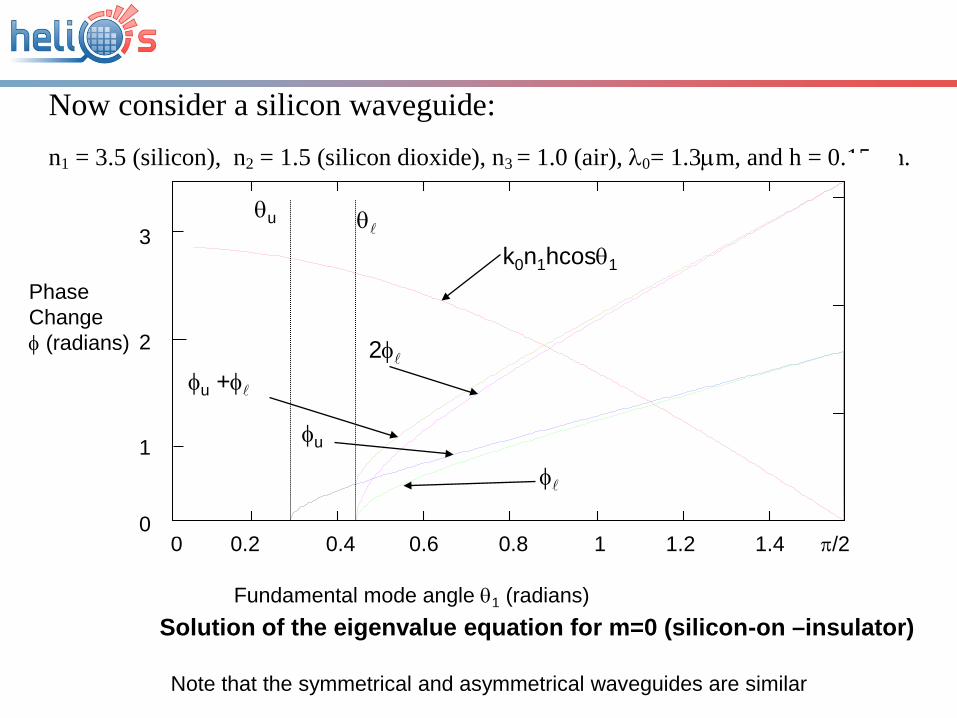
Now consider a silicon waveguide: n1 = 3.5 (silicon), n2 = 1.5 (silicon dioxide), n3 = 1.0 (air), λ0= 1.3µm, and h = 0.15µm.
0 0.2 0.4 0.6 0.8 1 1.2 1.40
1
2
3
f( )θ
θ2( )θ
θ1( )θ
θ3( )θ
θ4( )θ
θ
k0n1hcosθ1
2φ
φu
φ
Fundamental mode angle θ1 (radians)
θu θ
Phase Changeφ (radians)
Solution of the eigenvalue equation for m=0 (silicon-on –insulator)
π20 0.2 0.4 0.6 0.8 1 1.2 1.4 π/2
3
2
1
0
Note that the symmetrical and asymmetrical waveguides are similar
φu +φ
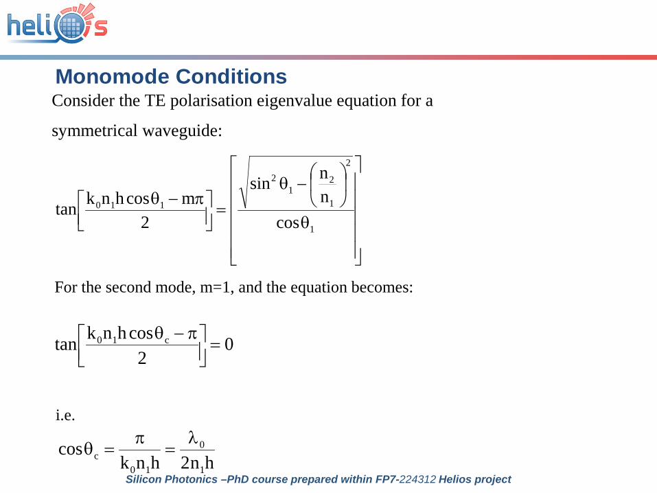
Monomode Conditions
Consider the TE polarisation eigenvalue equation for a
symmetrical waveguide:
θ
−θ
=
π−θ
1
2
1
21
2
110
cosnnsin
2mcoshnktan
For the second mode, m=1, and the equation becomes:
i.e.
02
coshnktan c10 =
π−θ
hn2hnkcos
1
0
10c
λ=
π=θ
Silicon Photonics –PhD course prepared within FP7-224312 Helios project
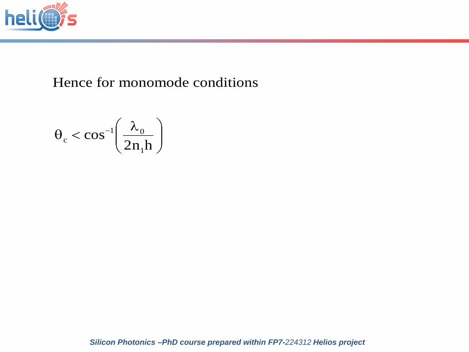
Hence for monomode conditions
λ<θ −
hn2cos
1
01c
Silicon Photonics –PhD course prepared within FP7-224312 Helios project

Effective Index We have seen that propagation constants in the z and y directions are:
and
101z sinknk θ=
101y cosknk θ=
kz is also known as β, the propagation constant in the direction of the waveguide
Now define a parameter N, called the effective index of the
mode, such that:
11 sinnN θ=
i.e.
0z Nkk =β=
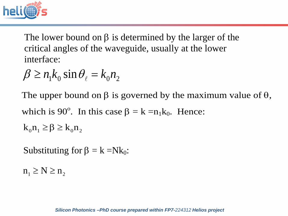
The lower bound on β is determined by the larger of the critical angles of the waveguide, usually at the lower interface:
2001 sin nkkn =≥ θβ
The upper bound on β is governed by the maximum value of θ,
which is 90o. In this case β = k =n1k0. Hence:
2010 nknk ≥β≥
Substituting for β = k =Nk0:
21 nNn ≥≥
Silicon Photonics –PhD course prepared within FP7-224312 Helios project

Just a little electromagnetic theory Starting with Maxwell’s equations, if we assume a loss-less, non conducting
medium, limit ourselves to propagation in the z direction, and consider one
polarisation at a time (TE or TM),we can derive a scalar equation describing
wave propagation in our planar waveguide:
2
2
2
2
2
2
tE
zE
yE x
mmxx
∂∂
=∂∂
+∂∂ εµ
where εm is the permittivity of the waveguide, µm is the permeability of the
waveguide, and in this case the electric field polarised in the x direction
corresponds to TE polarisaton. This is caliled the scalar wave equation.
Silicon Photonics –PhD course prepared within FP7-224312 Helios project
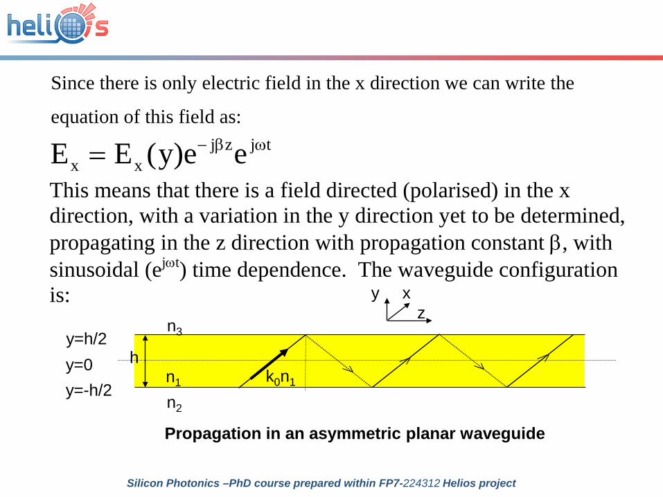
Since there is only electric field in the x direction we can write the
equation of this field as:
tjzjxx ey)e(EE ωβ−=
This means that there is a field directed (polarised) in the x direction, with a variation in the y direction yet to be determined, propagating in the z direction with propagation constant β, with sinusoidal (ejωt) time dependence. The waveguide configuration is:
Propagation in an asymmetric planar waveguide
n1
n2
n3
y x z
hk0n1y=-h/2
y=h/2y=0
Silicon Photonics –PhD course prepared within FP7-224312 Helios project
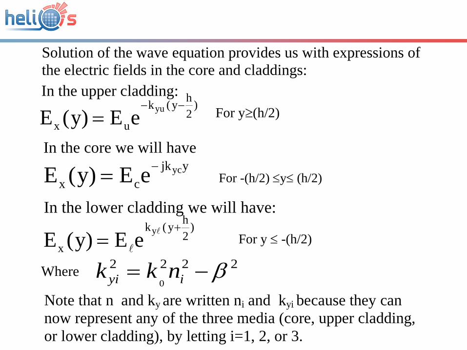
Solution of the wave equation provides us with expressions of the electric fields in the core and claddings:
In the upper cladding:
For y≥(h/2) )2hy(k
uxyueEy)(E
−−=
In the core we will have
For -(h/2) ≤y≤ (h/2) yjk
cxyceEy)(E −=
In the lower cladding we will have:
For y ≤ -(h/2) )
2hy(k
xyeEy)(E
+=
Where 22220
β−= iyi nkkNote that n and ky are written ni and kyi because they can now represent any of the three media (core, upper cladding, or lower cladding), by letting i=1, 2, or 3.
Propagation constants again In solving the wave equation we assumed field solutions with propagation constants in the core, and the upper and lower claddings, but we didn’t discuss why the propagation constants took the form they did.
Our general solution was of the form:
tjzjykcx eeeEE y ωβ−−=
However, in the three media, core, upper cladding and lower cladding, the propagation constant ky took different forms. In the claddings ky was a real number, whereas in the core ky was an imaginary number • total internal reflection occurs
• field decays in cladding
• part of the field propagates in the cladding
Mode Profiles Now that we have field solutions for modes in the planar
waveguide, we can plot the field distribution, Ex(y) or the
intensity distribution, Ex(y)2. Consider the following
waveguide:
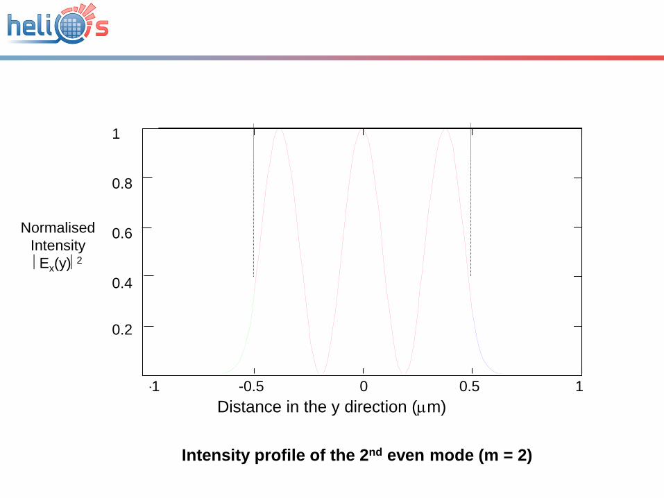
n1 = 3.5, n2 = 1.5, n3 = 1.0, λ0= 1.3µm, and h = 1.0µm.
For even functions, the field in the core is a cosine function, and in the claddings, an exponential decay. Therefore, solutions for m=0, and m=2 are even functions, and are plotted below. The field distribution is plotted for m = 0, and the intensity distribution is plotted for m = 2.
Silicon Photonics –PhD course prepared within FP7-224312 Helios project
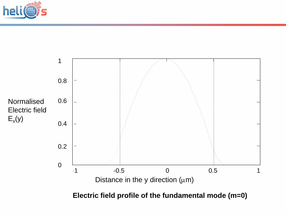
Electric field profile of the fundamental mode (m=0)
1 10 6 5 10 7 0 5 10 7 1 10 60
0.2
0.4
0.6
0.8
1
EC0 ( )y
EU0 ( )y2
EL0 ( )y1
,,y y2 y1
NormalisedElectric field Ex(y)
Distance in the y direction (µm)-1 -0.5 0 0.5 1
1
0.8
0.6
0.4
0.2
0
1 10 6 5 10 7 0 5 10 7 1 10 60
0.2
0.4
0.6
0.8
1
IC2( )y
IU2( )y2
IL2( )y1
,,y y2 y1
Normalised Intensity Ex(y)2
Distance in the y direction (µm)
Intensity profile of the 2nd even mode (m = 2)
-1 -0.5 0 0.5 1
1
0.8
0.6
0.4
0.2
0

Confinement factor
How much of the power propagates inside the core? We can define a confinement factor Γ:
∫
∫=Γ ∞
∞−
−
dy)y(E
dy)y(E
2x
2/h
2/h
2x
Silicon Photonics –PhD course prepared within FP7-224312 Helios project
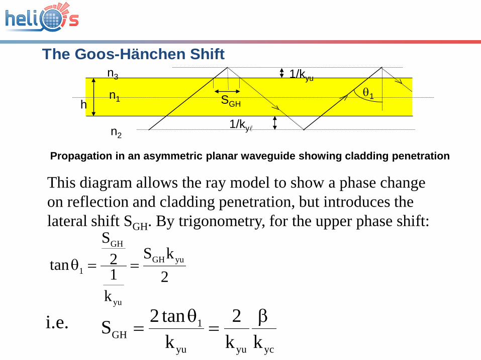
The Goos-Hänchen Shift
This diagram allows the ray model to show a phase change on reflection and cladding penetration, but introduces the lateral shift SGH. By trigonometry, for the upper phase shift:
Propagation in an asymmetric planar waveguide showing cladding penetration
n1
n2
n3
h
1/kyu
1/ky
SGHθ1
2kS
k12
S
tan yuGH
yu
GH
1 ==θ
i.e.
ycyuyu
1GH kk
2ktan2S β
=θ
=
Waveguide materialsPlanar waveguidesRib and ridge waveguidesStrip waveguidesLossesPolarisation issuesEffect of stress
Silicon Photonics –PhD course prepared within FP7-224312 Helios project
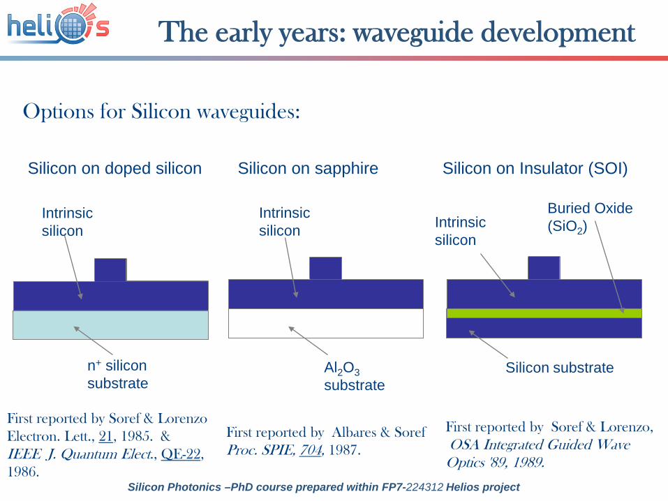
Options for Silicon waveguides:
Intrinsic silicon
n+ silicon substrate
Intrinsic silicon
Al2O3 substrate
Intrinsic silicon
Silicon substrate
Buried Oxide (SiO2)
Silicon on doped silicon Silicon on sapphire Silicon on Insulator (SOI)
First reported by Soref & Lorenzo Electron. Lett., 21, 1985. &IEEE J. Quantum Elect., QE-22, 1986.
First reported by Albares & SorefProc. SPIE, 704, 1987.
First reported by Soref & Lorenzo, OSA Integrated Guided Wave Optics '89, 1989.
The early years: waveguide development
Silicon Photonics –PhD course prepared within FP7-224312 Helios project

The most popular waveguides
Rib/ridge waveguide (H=200-400 nm to several microns; 0.1 dB/cm loss)
Strip waveguide (SM: 200×500 nm; 2-3 dB/cm loss)
W
D
t
t
h
H
Si
SiO2
Si
SiO2
Top oxide cover
Substrate
Buried oxide
Core
y
xz
θ
Photonic crystal waveguide (L=100 μm; 3-4 dB/cm loss)
Slot waveguide (non-linear effects, sensors)
Silicon Photonics –PhD course prepared within FP7-224312 Helios project
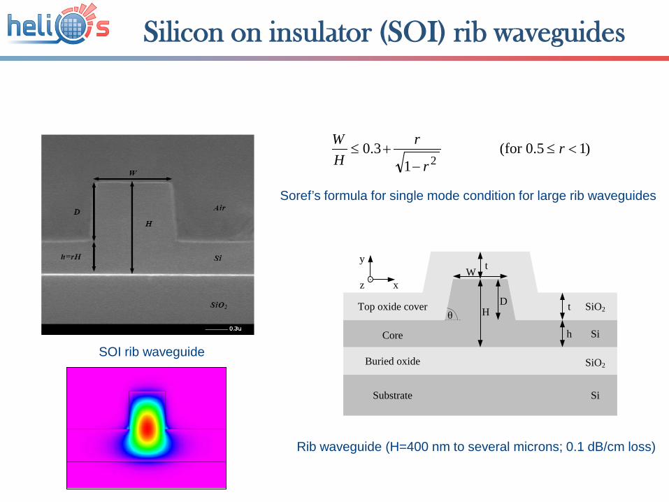
Silicon on insulator (SOI) rib waveguides
Soref’s formula for single mode condition for large rib waveguides
)15.0for(1
3.02
<≤−
+≤ rr
rHW
SOI rib waveguide
W
D
t
t
h
H
Si
SiO2
Si
SiO2
Top oxide cover
Substrate
Buried oxide
Core
y
xz
θ
Rib waveguide (H=400 nm to several microns; 0.1 dB/cm loss)
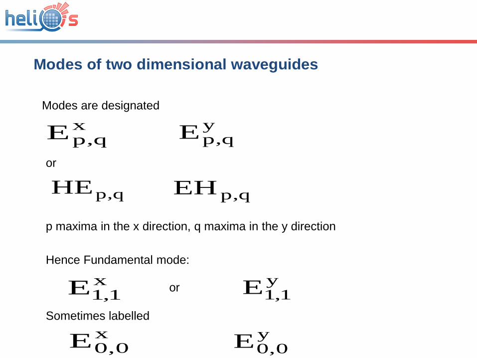
Modes of two dimensional waveguides
xq,pE
Modes are designated
yq,pE
or
q,pHE q,pEH
p maxima in the x direction, q maxima in the y direction
Hence Fundamental mode:
x1,1E or y
1,1ESometimes labelled
x0,0E y
0,0E
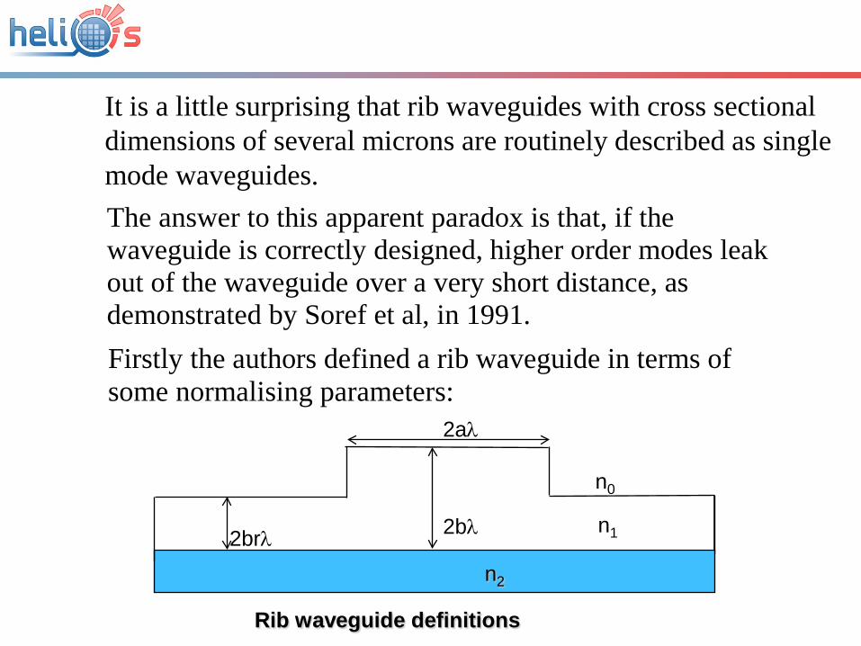
It is a little surprising that rib waveguides with cross sectional dimensions of several microns are routinely described as single mode waveguides.The answer to this apparent paradox is that, if the waveguide is correctly designed, higher order modes leak out of the waveguide over a very short distance, as demonstrated by Soref et al, in 1991. Firstly the authors defined a rib waveguide in terms of some normalising parameters:
n2
Rib waveguide definitions
2brλ 2bλ n1
n0
2aλ
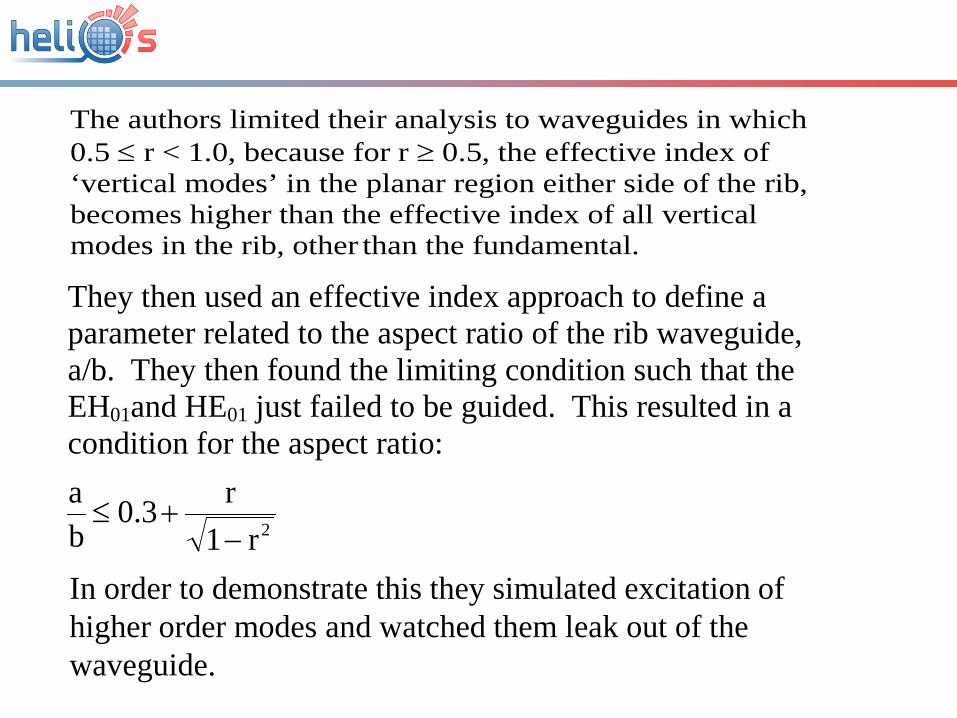
The authors limited their analysis to waveguides in which 0.5 ≤ r < 1.0, because for r ≥ 0.5, the effective index of ‘vertical modes’ in the planar region either side of the rib, becomes higher than the effective index of all vertical modes in the rib, other than the fundamental.
They then used an effective index approach to define a parameter related to the aspect ratio of the rib waveguide, a/b. They then found the limiting condition such that the EH01and HE01 just failed to be guided. This resulted in a condition for the aspect ratio:
2r1
r3.0ba
−+≤
In order to demonstrate this they simulated excitation of higher order modes and watched them leak out of the waveguide.

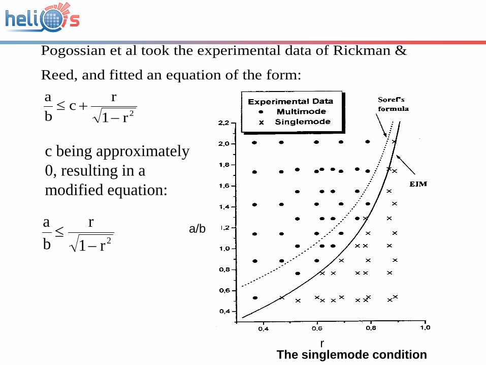
Pogossian et al took the experimental data of Rickman &
Reed, and fitted an equation of the form:
2r1
rcba
−+≤
2r1r
ba
−≤
The singlemode condition
a/b
r
c being approximately 0, resulting in a modified equation:
SOI rib waveguides – modelling
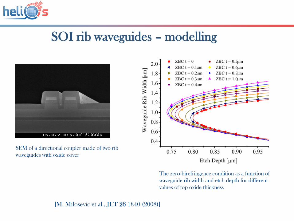
SEM of a directional coupler made of two rib waveguides with oxide cover
The zero-birefringence condition as a function of waveguide rib width and etch depth for different values of top oxide thickness
[M. Milosevic et al., JLT 26 1840 (2008)]
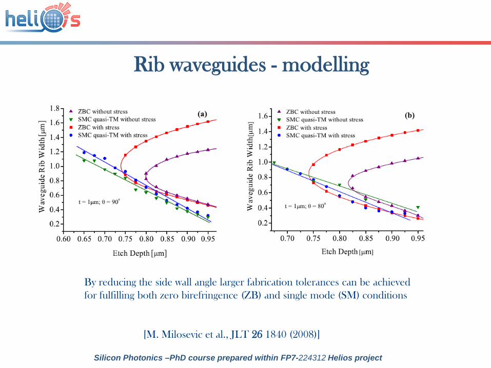
Rib waveguides - modelling
By reducing the side wall angle larger fabrication tolerances can be achieved for fulfilling both zero birefringence (ZB) and single mode (SM) conditions
[M. Milosevic et al., JLT 26 1840 (2008)]
Silicon Photonics –PhD course prepared within FP7-224312 Helios project

Rib waveguides – oxide thickness and side wall angle influence
Influence of the sidewall angle on polarisation independent propagation [M. Milosevic et al., JLT 2008]
By suitable selection of the waveguide dimensions and the oxide layer parameters, the additional stress can be used to allow greater flexibility in the design of the waveguide [G. Mashanovich et al., SST, 2008]
Silicon Photonics –PhD course prepared within FP7-224312 Helios project
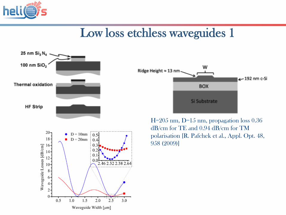
Low loss etchless waveguides 1
H=205 nm, D=15 nm, propagation loss 0.36 dB/cm for TE and 0.94 dB/cm for TM polarisation [R. Pafchek et al., Appl. Opt. 48, 958 (2009)]

Low loss etchless waveguides 2
H=70 nm, W = 1 um, loss 0.3 dB/cm, 0.007 dB/bend with R=50 um (0.15 dB/bend with R=10 um) [ J. Cardenas et al., OE 17, 4752 (2009)]
Silicon Photonics –PhD course prepared within FP7-224312 Helios project
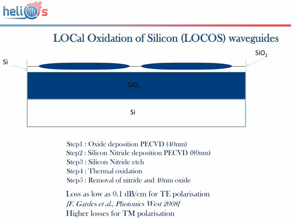
SiO2
Si
Si
Step1 : Oxide deposition PECVD (40nm)
SiO2
Step2 : Silicon Nitride deposition PECVD (80nm)
Si3N4
Step3 : Silicon Nitride etch
Step5 : Removal of nitride and 40nm oxideStep4 : Thermal oxidation
Loss as low as 0.1 dB/cm for TE polarisation [F. Gardes et al., Photonics West 2008]Higher losses for TM polarisation
LOCal Oxidation of Silicon (LOCOS) waveguides

Waveguide materialsPlanar waveguidesRib and ridge waveguidesStrip waveguidesLossesPolarisation issuesEffect of stress
Silicon Photonics –PhD course prepared within FP7-224312 Helios project
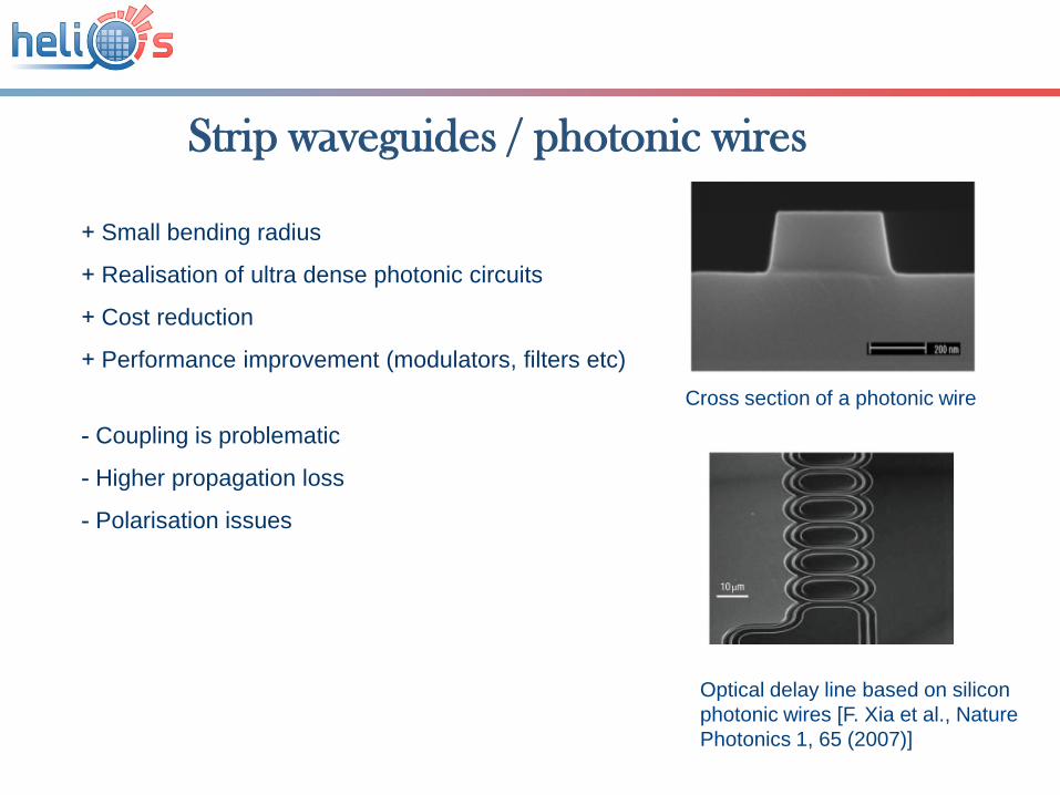
Strip waveguides / photonic wires
+ Small bending radius
+ Realisation of ultra dense photonic circuits
+ Cost reduction
+ Performance improvement (modulators, filters etc)
- Coupling is problematic
- Higher propagation loss
- Polarisation issues
Optical delay line based on silicon photonic wires [F. Xia et al., Nature Photonics 1, 65 (2007)]
Cross section of a photonic wire
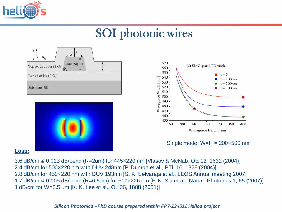
SOI photonic wires
Loss:
3.6 dB/cm & 0.013 dB/bend (R=2um) for 445×220 nm [Vlasov & McNab, OE 12, 1622 (2004)]2.4 dB/cm for 500×220 nm with DUV 248nm [P. Dumon et al., PTL 16, 1328 (2004)]2.8 dB/cm for 450×220 nm with DUV 193nm [S. K. Selvaraja et al., LEOS Annual meeting 2007]1.7 dB/cm & 0.005 dB/bend (R=6.5um) for 510×226 nm [F. N. Xia et al., Nature Photonics 1, 65 (2007)]1 dB/cm for W=0.5 um [K. K. Lee et al., OL 26, 1888 (2001)]
Single mode: W×H = 200×500 nm
Silicon Photonics –PhD course prepared within FP7-224312 Helios project
Poly-Si: 6.5 dB/cm for 700×250 nm waveguides [Q. Fang et al., OE 16, 6425 (2008)]
a-Si: 3.5 dB/cm for 480×220 nm waveguides [S. K. Selvaraja, Opt. Comm. 282, 1767 (2009)]
SiN: 1.5 dB/cm for 310×1050 nm waveguides[T. Barwicz et al., OE 12, 1437 (2004)]
Other silicon based waveguide materials
Silicon Photonics –PhD course prepared within FP7-224312 Helios project

Waveguide materialsPlanar waveguidesRib and ridge waveguidesStrip waveguidesLossesPolarisation issuesEffect of stress
Silicon Photonics –PhD course prepared within FP7-224312 Helios project
Refractive index and loss coefficient in optical waveguides Complex refractive index can be defined as:
IR jnn'n +=
And we have expressed a propagating field as:
)tkz(j
0eEE ω−=Substituting for propagation constant and complex refractive index: tjznkznjk
0)tz'nk(j
0 e.e.e.EeEE I0R00 ω−−ω− ==
The term exp(-k0nIz) is often re-designated . The term α is called the loss coefficient. The factor of ½ is included in the definition above because α is an intensity loss coefficient. Therefore we can write :
)21exp( α−
z
0eII α−=The benchmark for acceptable waveguide loss is of the order of 1dB/cm. Typical losses for SOI rib waveguides are in the range 0.1 - 0.5 dB/cm
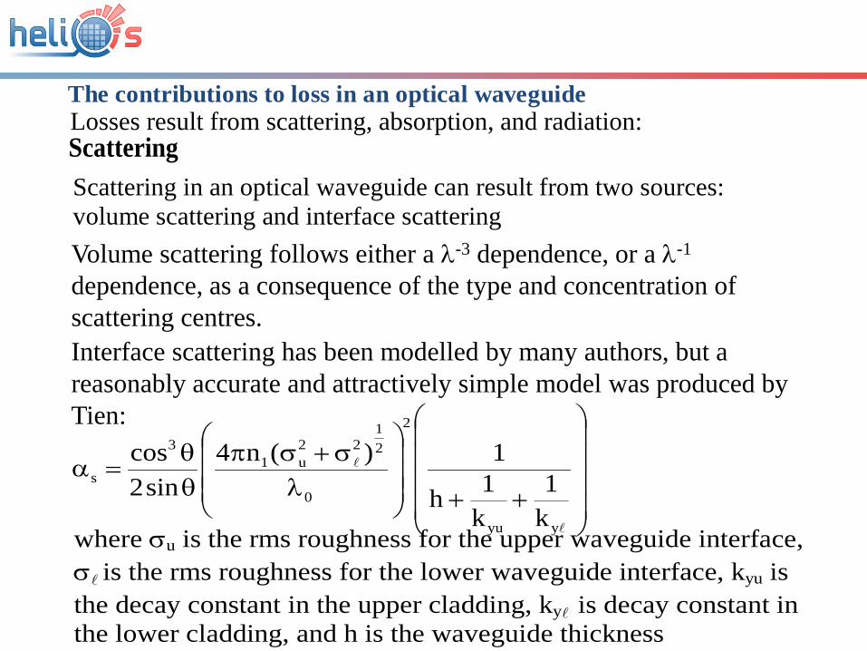
The contributions to loss in an optical waveguide
Scattering Losses result from scattering, absorption, and radiation:
Scattering in an optical waveguide can result from two sources: volume scattering and interface scattering Volume scattering follows either a λ-3 dependence, or a λ-1
dependence, as a consequence of the type and concentration of scattering centres.Interface scattering has been modelled by many authors, but a reasonably accurate and attractively simple model was produced by Tien:
where σu is the rms roughness for the upper waveguide interface, σ is the rms roughness for the lower waveguide interface, kyu is the decay constant in the upper cladding, ky is decay constant in the lower cladding, and h is the waveguide thickness
++
λσ+σπ
θθ
=α
yyu
2
0
21
22u1
3
s
k1
k1h
1)(n4sin2
cos
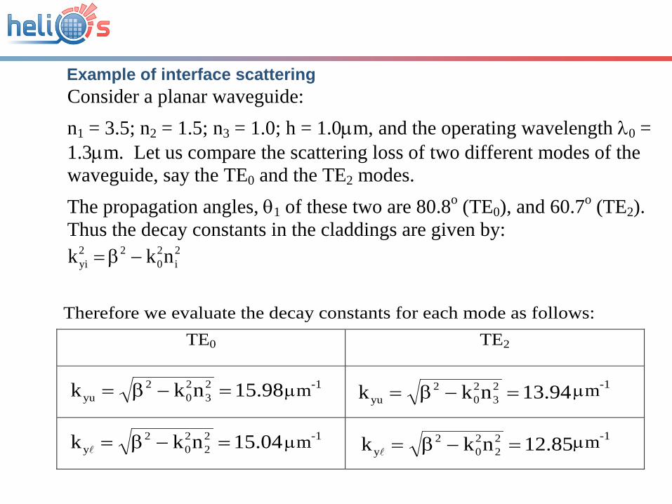
Example of interface scatteringConsider a planar waveguide: n1 = 3.5; n2 = 1.5; n3 = 1.0; h = 1.0µm, and the operating wavelength λ0 = 1.3µm. Let us compare the scattering loss of two different modes of the waveguide, say the TE0 and the TE2 modes. The propagation angles, θ1 of these two are 80.8o (TE0), and 60.7o (TE2). Thus the decay constants in the claddings are given by:
2i
20
22yi nkk −β=
Therefore we evaluate the decay constants for each mode as follows: TE0 TE2
µm-1 µm-1
µm-1 µm-1
98.15nkk 23
20
2yu =−β= 94.13nkk 2
320
2yu =−β=
04.15nkk 22
20
2y =−β= 85.12nkk 2
220
2y =−β=
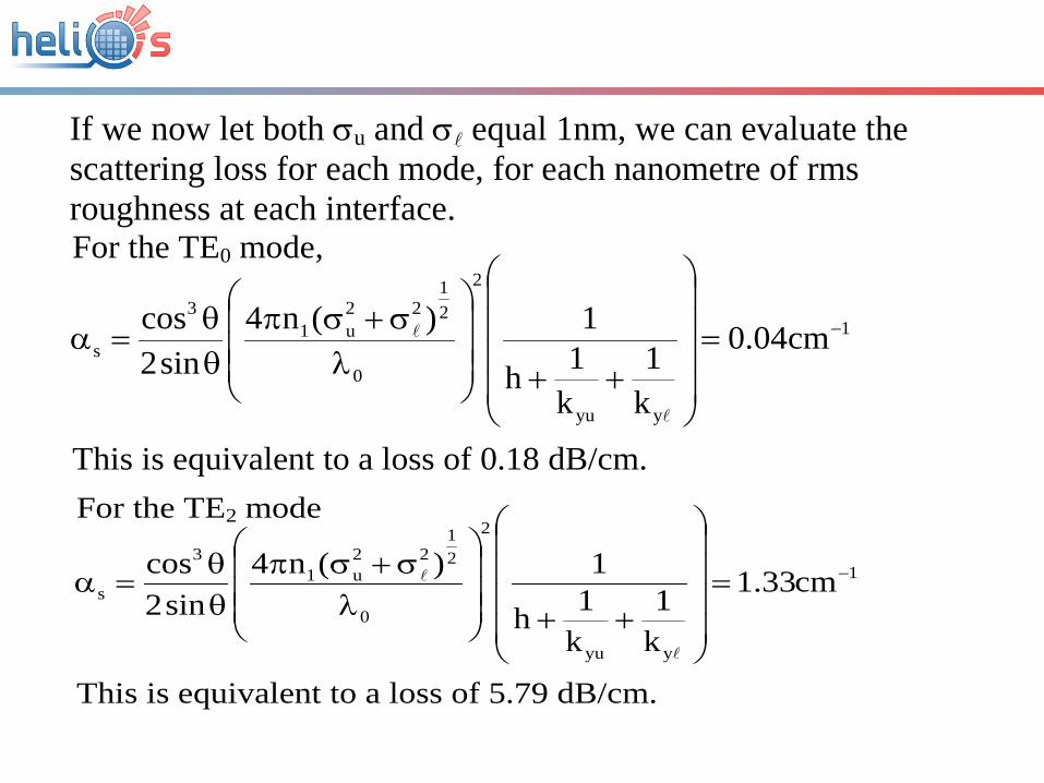
If we now let both σu and σ equal 1nm, we can evaluate the scattering loss for each mode, for each nanometre of rms roughness at each interface. For the TE0 mode,
This is equivalent to a loss of 0.18 dB/cm.
1
yyu
2
0
21
22u1
3
s cm04.0
k1
k1h
1)(n4sin2
cos −=
++
λσ+σπ
θθ
=α
For the TE2 mode
This is equivalent to a loss of 5.79 dB/cm.
1
yyu
2
0
21
22u1
3
s cm33.1
k1
k1h
1)(n4sin2
cos −=
++
λσ+σπ
θθ
=α

Absorption The two main potential sources of absorption loss for semiconductor waveguides are band edge absorption and free carrier absorption. If we operate at a wavelength well away from the band edge, the former is negligible.
Changes in free carrier absorption can be described by Drude-Lorenz equation:
where e is the electronic charge; c is the velocity of light in vacuum; µe is the electron mobility; µh is the hole mobility; is the effective mass of electrons; is the effective mass of holes; Ne is the free electron concentration; ; Nh is the free hole concentration; ε0 is the permittivity of free space; and λ0 is the free space wavelength.
µ
+µεπ
λ=α∆ 2*
chh
h2*
cee
e
032
20
3
)m(N
)m(N
nc4e
*cem
*chm
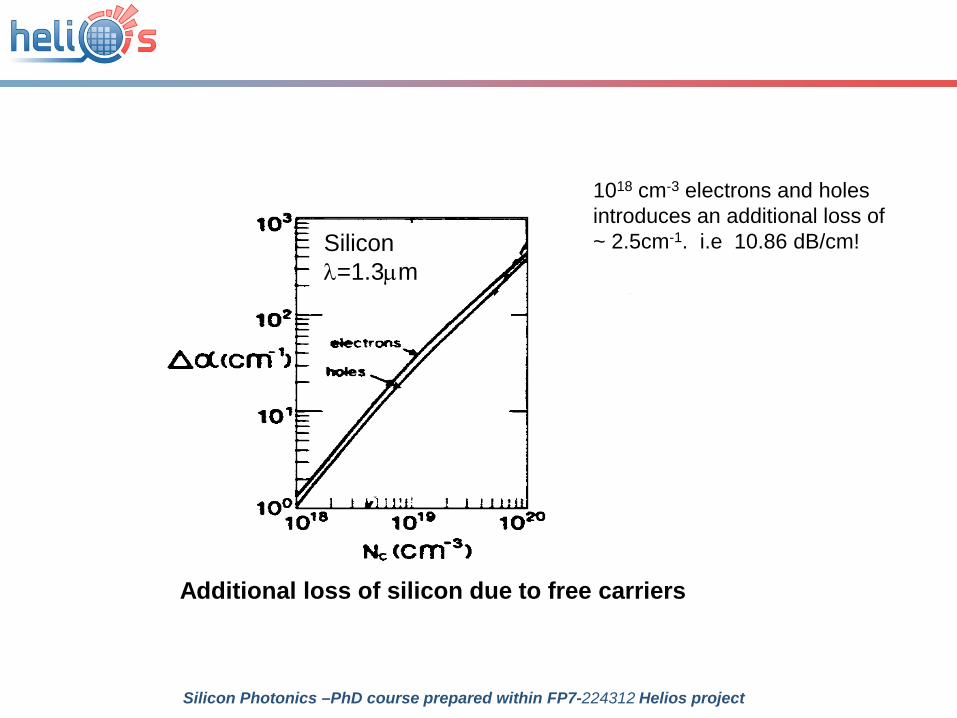
Additional loss of silicon due to free carriers
Siliconλ=1.3µm
1018 cm-3 electrons and holes introduces an additional loss of ~ 2.5cm-1. i.e 10.86 dB/cm!
Silicon Photonics –PhD course prepared within FP7-224312 Helios project

Radiation Losses in optical waveguides
Ideally negligible.
Possibility of radiation via leaky modes or curvature at too fast a rate.
Silicon Photonics –PhD course prepared within FP7-224312 Helios project
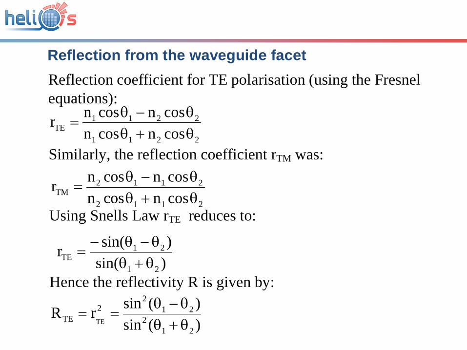
Reflection from the waveguide facet Reflection coefficient for TE polarisation (using the Fresnel equations):
2211
2211TE cosncosn
cosncosnrθ+θθ−θ
=
Similarly, the reflection coefficient rTM was:
2112
2112TM cosncosn
cosncosnrθ+θθ−θ
=
Using Snells Law rTE reduces to:
)sin()sin(r
21
21TE θ+θ
θ−θ−=
Hence the reflectivity R is given by:
)(sin)(sinrR
212
212
2TE TE θ+θ
θ−θ==
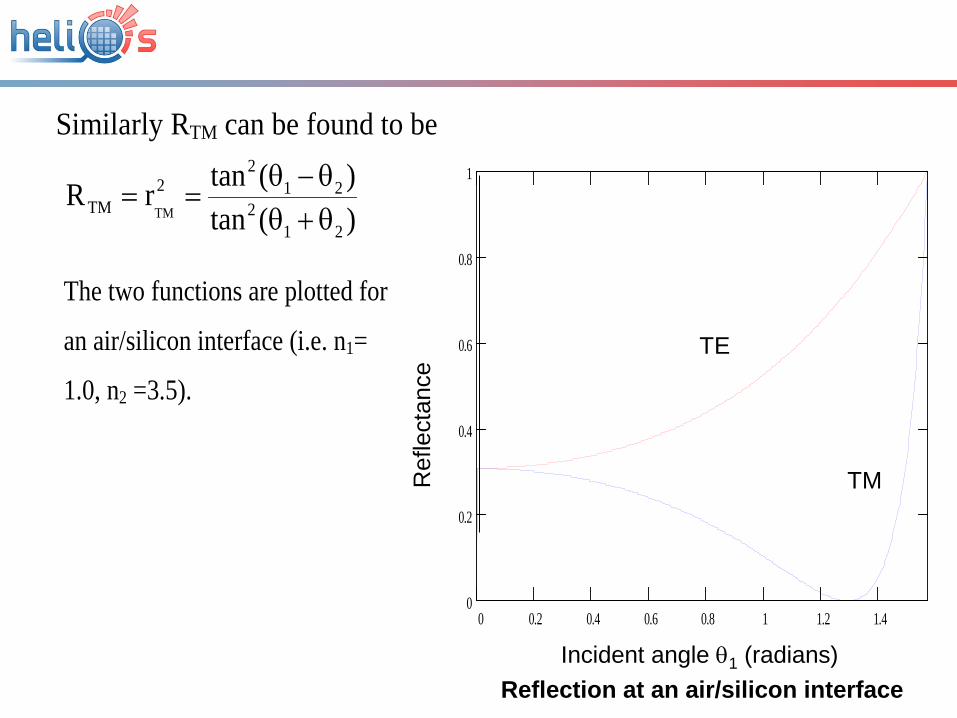
Similarly RTM can be found to be
)(tan)(tanrR
212
212
2TM TM θ+θ
θ−θ==
The two functions are plotted for
an air/silicon interface (i.e. n1=
1.0, n2 =3.5).
0 0.2 0.4 0.6 0.8 1 1.2 1.40
0.2
0.4
0.6
0.8
1
RTE( )θ1
RTM( )θ1
θ1Incident angle θ1 (radians)
Ref
lect
ance
TM
TE
Reflection at an air/silicon interface
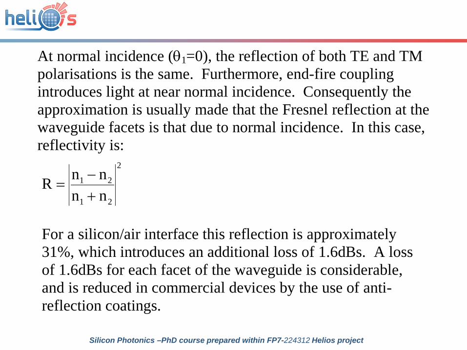
At normal incidence (θ1=0), the reflection of both TE and TM polarisations is the same. Furthermore, end-fire coupling introduces light at near normal incidence. Consequently the approximation is usually made that the Fresnel reflection at the waveguide facets is that due to normal incidence. In this case, reflectivity is:
2
21
21
nnnnR
+−
=
For a silicon/air interface this reflection is approximately 31%, which introduces an additional loss of 1.6dBs. A loss of 1.6dBs for each facet of the waveguide is considerable, and is reduced in commercial devices by the use of anti-reflection coatings.
Silicon Photonics –PhD course prepared within FP7-224312 Helios project

An anti-reflection coating has a thickness of λ/4, reducing or eliminating the reflection. For normal incidence, the net reflectivity R is given by:
where nar is the refractive index of the anti-reflection coating. R will be zero if:
2
2ar21
2ar21
nnnnnnR
+−
=
For a silicon/air interface, nar needs to be approximately 1.87.
For silicon nitride (Si3N4), n = 2.05.
For silicon oxynitride (SiOxNy), n ranges from 1.46 (SiO2) to
2.05 (Si3N4)
2ar21 nnn =
Silicon Photonics –PhD course prepared within FP7-224312 Helios project
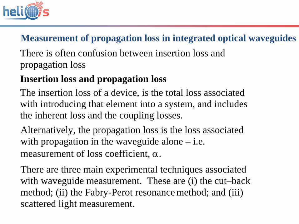
Measurement of propagation loss in integrated optical waveguides There is often confusion between insertion loss and propagation loss Insertion loss and propagation loss The insertion loss of a device, is the total loss associated with introducing that element into a system, and includes the inherent loss and the coupling losses. Alternatively, the propagation loss is the loss associated with propagation in the waveguide alone – i.e. measurement of loss coefficient, α. There are three main experimental techniques associated with waveguide measurement. These are (i) the cut–back method; (ii) the Fabry-Perot resonance method; and (iii) scattered light measurement.

The cut-back method The cut back method is conceptually simple. A waveguide of length L1 is excited by one of the coupling methods mentioned, and the output power from the waveguide, I1, and the input power to the waveguide, I0 are recorded. The waveguide is then shortened to another length, L2, and the measurement repeated to determine I2. Hence:
i.e.
))LL(exp(II
212
1 −α−=
−
=α1
2
21 IIln
LL1
Silicon Photonics –PhD course prepared within FP7-224312 Helios project
The accuracy of the technique can be improved by taking multiple measurements and plotting a graph
Optical Loss(dBs)
Propagation length (cm)
Note that the data presented is now insertion loss for each device length, not propagation loss. Hence the loss at zero propagation loss represents coupling loss.
A useful variation of the cut-back method, is to carry out an insertion loss measurement for a single waveguide length, and calculate the coupling. Whilst this technique is less, it has the enormous advantage of being non-destructive
The Fabry-Perot resonance method An optical waveguide with polished end faces (facets), is similar in
structure to the cavity of a laser, and may be regarded as a
potentially resonant cavity. Such a cavity is called a Fabry-Perot
cavity. The optical intensity transmitted through such a cavity, It,
is related to the incident light intensity, I0, by the well known
equation:
where R is the facet reflectivity, L is the waveguide length, α is the loss coefficient, and φ is the phase difference between successive waves in the cavity
)2
(sinRe4)Re1(
e)R1(II
2L2L
L2
0
t
φ+−
−=
α−α−
α−
Silicon Photonics –PhD course prepared within FP7-224312 Helios project
This transfer function has a maximum value when φ=0 (or multiples of 2π), and a minimum value when φ=π. i.e. :
2L
L2
L2L
L2
0
min
)Re1(e)R1(
Re4)Re1(e)R1(
II
α−
α−
α−α−
α−
+−
=+−
−=
2L
L2
0
max
)Re1(e)R1(
II
α−
α−
−−
=
Which we can rearrange as:
+ζ−ζ
−=α11
R1ln
L1
If we know the reflectivity, R, if we can measure ζ, the loss coefficient can be evaluated. Therefore if we can sweep through a few cycles of 2π, ζ can be measured. Such cycling can be achieved thermally, or by varying the wavelength of the light source.
Therefore the ratio of the maximum intensity to minimum intensity, ζ, is:
2L
2L
min
max
)Re1()Re1(
II
α−
α−
−+
==ζ
0 5 10 15 20 250
0.2
0.4
0.6
0.8
11
0
FP1 θ( )
FP2 θ( )
FP3 θ( )
8 π⋅0 θ
Plot of the Fabry-Perot transfer function for three different mirror reflectivities
R=0.5
R=0.31
R=0.1
It/I0
φ (radians)
Imin Imax
Silicon Photonics –PhD course prepared within FP7-224312 Helios project
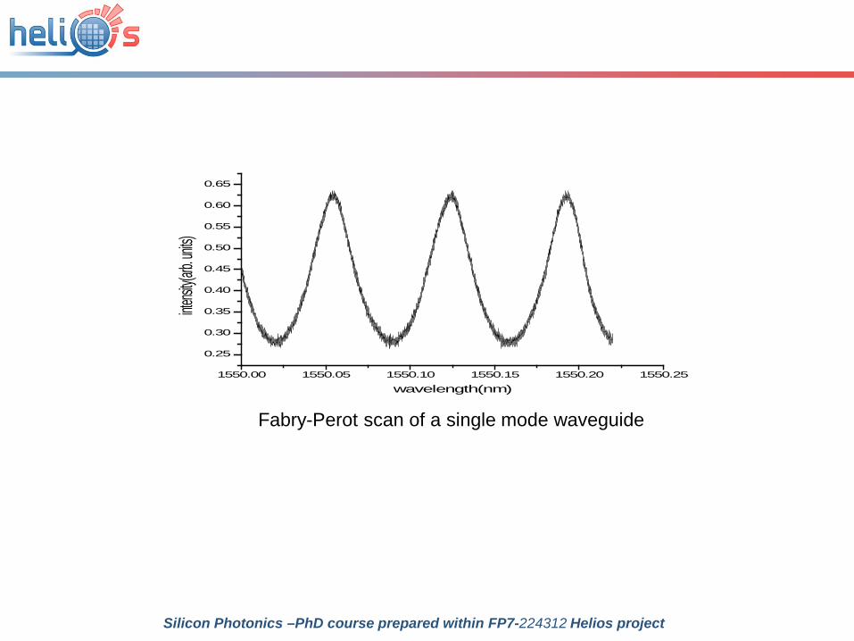
1550.00 1550.05 1550.10 1550.15 1550.20 1550.25
0.25
0.30
0.35
0.40
0.45
0.50
0.55
0.60
0.65inte
nsity(a
rb. uni
ts)
wavelength(nm)
Fabry-Perot scan of a single mode waveguide
Silicon Photonics –PhD course prepared within FP7-224312 Helios project
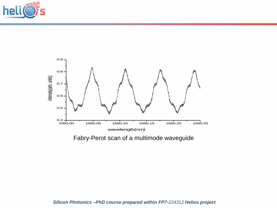
Fabry-Perot scan of a multimode waveguide
1550.00 1550.05 1550.10 1550.15 1550.20 1550.250.4
0.5
0.6
0.7
0.8
0.9
intensit
y(arb.
units)
wavelength(nm)
Silicon Photonics –PhD course prepared within FP7-224312 Helios project

Scattered Light Measurement
The measurement of scattered light from the surface of a waveguide can be used to
determine the loss. The assumption is that the amount of light scattered is proportional to
the propagating light. Therefore, the rate of decay of scattered light with length will mimic
the rate of decay of light in the waveguide.
However, it is clear that light is only scattered significantly if the loss of the waveguide is
high, so this approach has limited uses.
Silicon Photonics –PhD course prepared within FP7-224312 Helios project
Waveguide materialsPlanar waveguidesRib and ridge waveguidesStrip waveguidesLossesPolarisation issuesEffect of stress
Silicon Photonics –PhD course prepared within FP7-224312 Helios project

What is polarisation?
Light is an electromagnetic wave, which has the characteristic of both electric and magnetic fields that vary with time.
Sinusoidal plane wave showing electric and magnetic fields
Consider a sinusoidal plane wave:
This figure shows 3 characteristics:
Silicon Photonics –PhD course prepared within FP7-224312 Helios project
1. The wave is a plane wave because the value of the electric field (shown in the x direction) and the magnetic field (shown in the y direction), are constant in any z-plane.
2. Secondly, the wave is transverse because both the electric and magnetic fields are transverse to the direction of propagation (z direction).
3. The wave is polarised, because the electric and magnetic field exist in only a single direction. This particular wave is polarised in the x direction because the electric field exists only in the x direction.
There are various forms of polarisation, but the most important waves for optical circuits are plane polarised or unpolarised (random).
Silicon Photonics –PhD course prepared within FP7-224312 Helios project
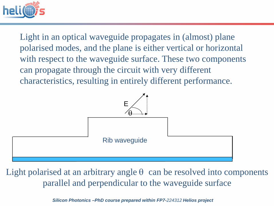
Light in an optical waveguide propagates in (almost) plane polarised modes, and the plane is either vertical or horizontal with respect to the waveguide surface. These two components can propagate through the circuit with very different characteristics, resulting in entirely different performance.
Light polarised at an arbitrary angle θ can be resolved into components parallel and perpendicular to the waveguide surface
θE
Rib waveguide
Silicon Photonics –PhD course prepared within FP7-224312 Helios project
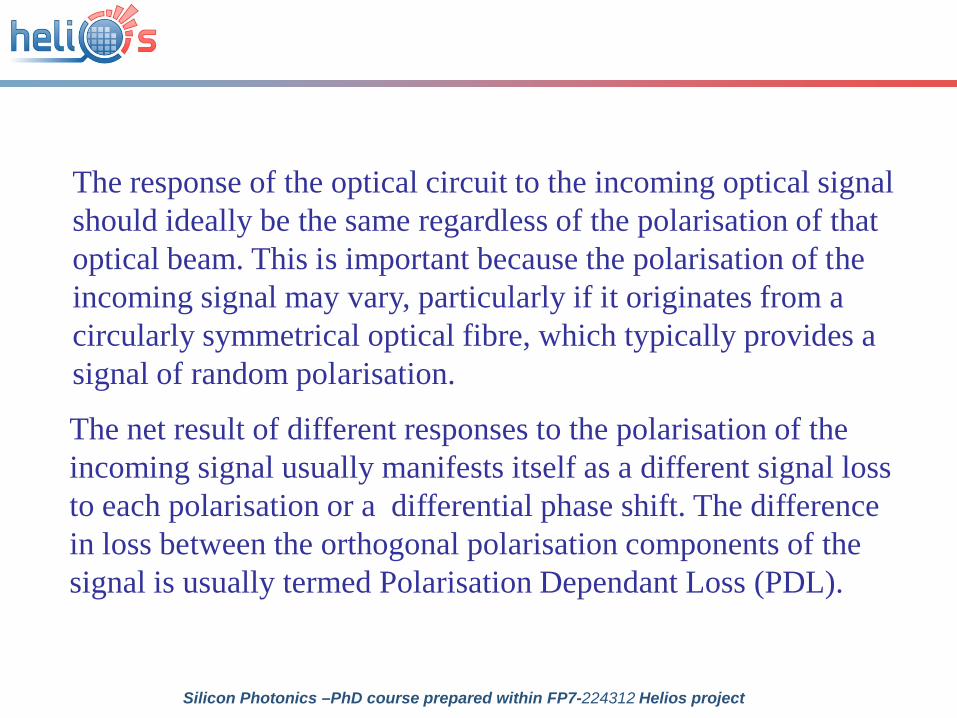
The response of the optical circuit to the incoming optical signal should ideally be the same regardless of the polarisation of that optical beam. This is important because the polarisation of the incoming signal may vary, particularly if it originates from a circularly symmetrical optical fibre, which typically provides a signal of random polarisation.
The net result of different responses to the polarisation of the incoming signal usually manifests itself as a different signal loss to each polarisation or a differential phase shift. The difference in loss between the orthogonal polarisation components of the signal is usually termed Polarisation Dependant Loss (PDL).
Silicon Photonics –PhD course prepared within FP7-224312 Helios project
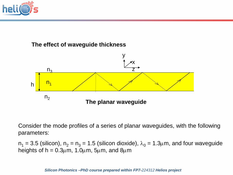
The effect of waveguide thickness
The planar waveguide
n1
n2
n3
y x z
h
Consider the mode profiles of a series of planar waveguides, with the following parameters:
n1 = 3.5 (silicon), n2 = n3 = 1.5 (silicon dioxide), λ0 = 1.3µm, and four waveguide heights of h = 0.3µm, 1.0µm, 5µm, and 8µm
Silicon Photonics –PhD course prepared within FP7-224312 Helios project

1 10 6 5 10 7 0 5 10 7 1 10 60
0.2
0.4
0.6
0.8
1
IC0TM( )y
IU0TM( )y2
IL0TM( )y1
,,y y2 y11 10 6 5 10 7 0 5 10 7 1 10 60
0.2
0.4
0.6
0.8
1
IC0TE( )y
IU0TE( )y2
IL0TE( )y1
,,y y2 y1
TETM
-1 -0.5 0 0.5 1
Distance in the y direction (µm)
1
0.8
0.6
0.4
0.2
0
TE and TM intensity profiles for h = 1µm
3 10 7 2 10 7 1 10 7 0 1 10 7 2 10 7 3 10 70
0.2
0.4
0.6
0.8
1
IC0TM( )y
IU0TM( )y2
IL0TM( )y1
,,y y2 y13 10 7 2 10 7 1 10 7 0 1 10 7 2 10 7 3 10 70
0.2
0.4
0.6
0.8
1
IC0TE( )y
IU0TE( )y2
IL0TE( )y1
,,y y2 y1
TETM
-0.3 -0.2 -0.1 0 0.1 0.2 0.3
Distance in the y direction (µm)
1
0.8
0.6
0.4
0.2
0
TE and TM intensity profiles for h = 0.3µm
4 10 6 2 10 6 0 2 10 6 4 10 60
0.2
0.4
0.6
0.8
1
IC0TE( )y
IU0TE( )y2
IL0TE( )y1
,,y y2 y14 10 6 2 10 6 0 2 10 6 4 10 60
0.2
0.4
0.6
0.8
1
IC0TM( )y
IU0TM( )y2
IL0TM( )y1
,,y y2 y1
TETM
-5 -4 -3 -2 0 2 3 4 5
1
0.8
0.6
0.4
0.2
0
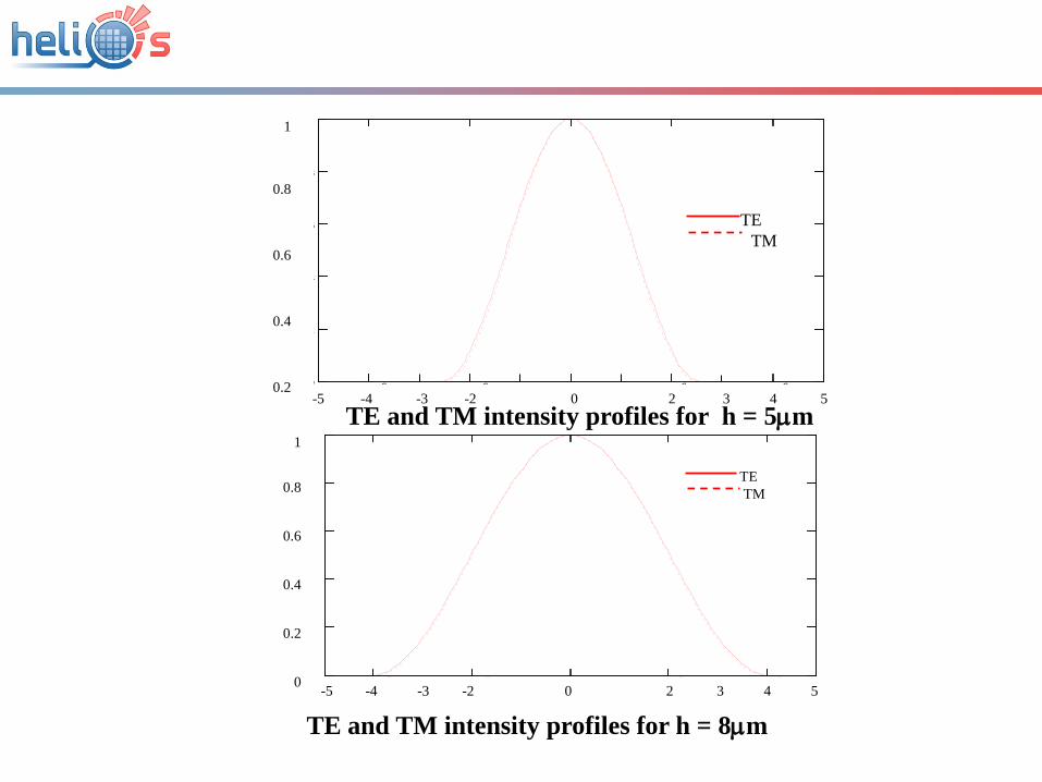
TE and TM intensity profiles for h = 5µm
TETM
4 10 6 2 10 6 0 2 10 6 4 10 60
0.2
0.4
0.6
0.8
1
IC0TE( )y
IU0TE( )y2
IL0TE( )y1
,,y y2 y14 10 6 2 10 6 0 2 10 6 4 10 60
0.2
0.4
0.6
0.8
1
IC0TM( )y
IU0TM( )y2
IL0TM( )y1
,,y y2 y1-5 -4 -3 -2 0 2 3 4 5
1
0.8
0.6
0.4
0.2
0
TE and TM intensity profiles for h = 8µm

Confinement is different for TE and TM modes
Polarisation dependence reduces with increasing waveguide height
Even for the larger waveguides, polarisation dependence is not removed
3 10 6 3.5 10 6 4 10 6 4.5 10 60
0.01
0.02
0.03
0.04
0.05
IC0TM( )y
IU0TM( )y2
,y y23 10 6 3.5 10 6 4 10 6 4.5 10 60
0.01
0.02
0.03
0.04
0.05
IC0TE( )y
IU0TE( )y2
,y y2
Enlarged view of the TE and TM mode profiles for h=8µm
3 3.5 4 4.5
Distance in the y direction (µm)
0.05
0.04
0.03
0.02
0.01
0
Nor
mal
ised
Inte
nsity

The differences in confinement of the modes can be understood by considering again, the graphical solution of the eigenvalue equation. If we plot both the TE and the TM eigenvalue equations on the same axes, it is clear that the phase change on reflection for the TM mode is always greater than that for the TE mode.
Recall that the y-directed propagation constant was given by:
Since θ1 is larger for the TE mode, then ‘cos θ1
’ is smaller for the TE mode, and hence the propagation constant ky is also smaller
101y cosknk θ=
Silicon Photonics –PhD course prepared within FP7-224312 Helios project
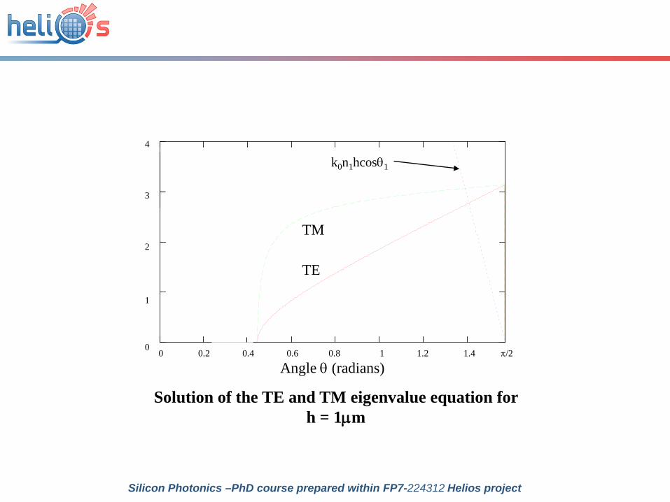
0 0.2 0.4 0.6 0.8 1 1.2 1.40
1
2
3
4
θTE( )θ
f0TE( )θ
θTM( )θ
θ0 0.2 0.4 0.6 0.8 1 1.2 1.4 π/2
Angle θ (radians)
4
3
2
1
0
TM
TE
k0n1hcosθ1
Solution of the TE and TM eigenvalue equation for h = 1µm
Silicon Photonics –PhD course prepared within FP7-224312 Helios project
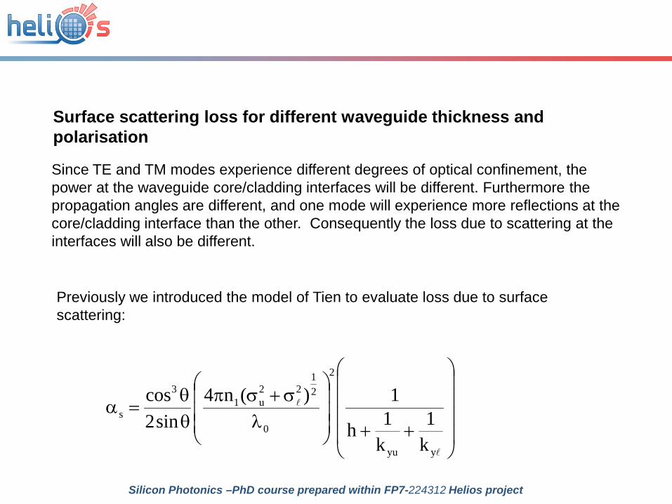
Surface scattering loss for different waveguide thickness and polarisation
Since TE and TM modes experience different degrees of optical confinement, the power at the waveguide core/cladding interfaces will be different. Furthermore the propagation angles are different, and one mode will experience more reflections at the core/cladding interface than the other. Consequently the loss due to scattering at the interfaces will also be different.
Previously we introduced the model of Tien to evaluate loss due to surface scattering:
++
λσ+σπ
θθ
=α
yyu
2
0
21
22u1
3
s
k1
k1h
1)(n4sin2
cos
Silicon Photonics –PhD course prepared within FP7-224312 Helios project
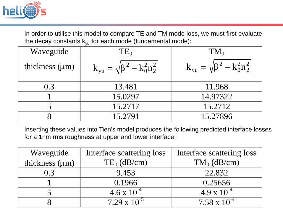
In order to utilise this model to compare TE and TM mode loss, we must first evaluate the decay constants kyu for each mode (fundamental mode):
Waveguide
thickness (µm)
TE0
TM0
0.3 13.481 11.968 1 15.0297 14.97322 5 15.2717 15.2712
8 15.2791 15.27896
22
20
2yu nkk −β= 2
220
2yu nkk −β=
Inserting these values into Tien’s model produces the following predicted interface losses for a 1nm rms roughness at upper and lower interface:
Waveguide thickness (µm)
Interface scattering loss TE0 (dB/cm)
Interface scattering loss TM0 (dB/cm)
0.3 9.453 22.832 1 0.1966 0.25656 5 4.6 x 10⁻⁴ 4.9 x 10⁻⁴
8 7.29 x 10⁻⁵ 7.58 x 10⁻⁴
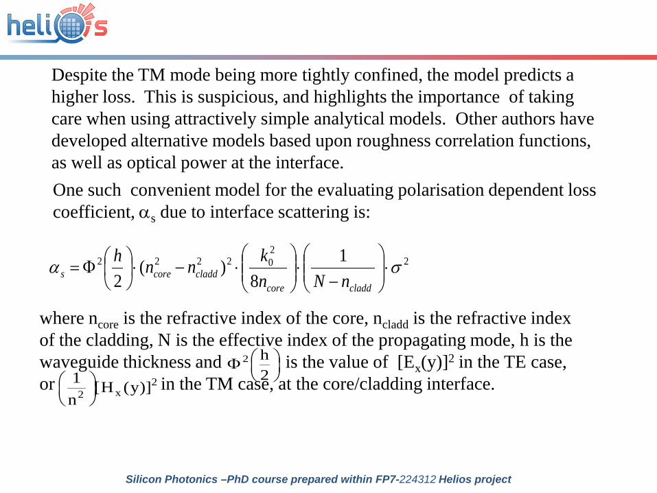
One such convenient model for the evaluating polarisation dependent loss coefficient, αs due to interface scattering is:
2202222 1
8)(
2σα ⋅
−
⋅
⋅−⋅
Φ=
claddcorecladdcores nNn
knnh
where ncore is the refractive index of the core, ncladd is the refractive index of the cladding, N is the effective index of the propagating mode, h is the waveguide thickness and is the value of [Ex(y)]2 in the TE case, or in the TM case, at the core/cladding interface.
Φ
2h2
2x2 )]y(H[
n1
Despite the TM mode being more tightly confined, the model predicts a higher loss. This is suspicious, and highlights the importance of taking care when using attractively simple analytical models. Other authors have developed alternative models based upon roughness correlation functions, as well as optical power at the interface.
Silicon Photonics –PhD course prepared within FP7-224312 Helios project
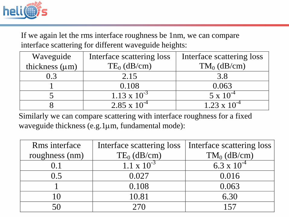
If we again let the rms interface roughness be 1nm, we can compare interface scattering for different waveguide heights:
Waveguide thickness (µm)
Interface scattering loss TE0 (dB/cm)
Interface scattering loss TM0 (dB/cm)
0.3 2.15 3.8 1 0.108 0.063 5 1.13 x 10⁻³ 5 x 10⁻⁴
8 2.85 x 10⁻⁴ 1.23 x 10⁻⁴
Similarly we can compare scattering with interface roughness for a fixed waveguide thickness (e.g.1µm, fundamental mode):
Rms interface roughness (nm)
Interface scattering loss TE0 (dB/cm)
Interface scattering loss TM0 (dB/cm)
0.1 1.1 x 10⁻³ 6.3 x 10⁻⁴
0.5 0.027 0.016 1 0.108 0.063 10 10.81 6.30 50 270 157

For comparison, consider interface scattering for a 5µm waveguide:
Rms interface roughness (nm)
Interface scattering loss TE0 (dB/cm)
Interface scattering loss TM0 (dB/cm)
0.1 1.13 x 10⁻⁵ 5 x 10⁻⁶
0.5 2.83 x 10⁻⁴ 1.25 x 10⁻⁴
1 1.13 x 10⁻³ 5 x 10⁻⁴
10 0.113 0.05 50 2.83 1.25
It is clear that the polarisation dependant loss can become important if either the interface quality is not kept under control, or if the device is very long. For example the interface roughness of the silicon/buried oxide layer of commercially available SIMOX wafers is typically in the range 0.8nm to 3nm. Even if we assume the surface of such wafers is perfectly smooth, this model suggests a loss ranging from 0.04 dB/cm to 0.57 dB/cm for the fundamental TM mode of a 1µm waveguide.
Silicon Photonics –PhD course prepared within FP7-224312 Helios project
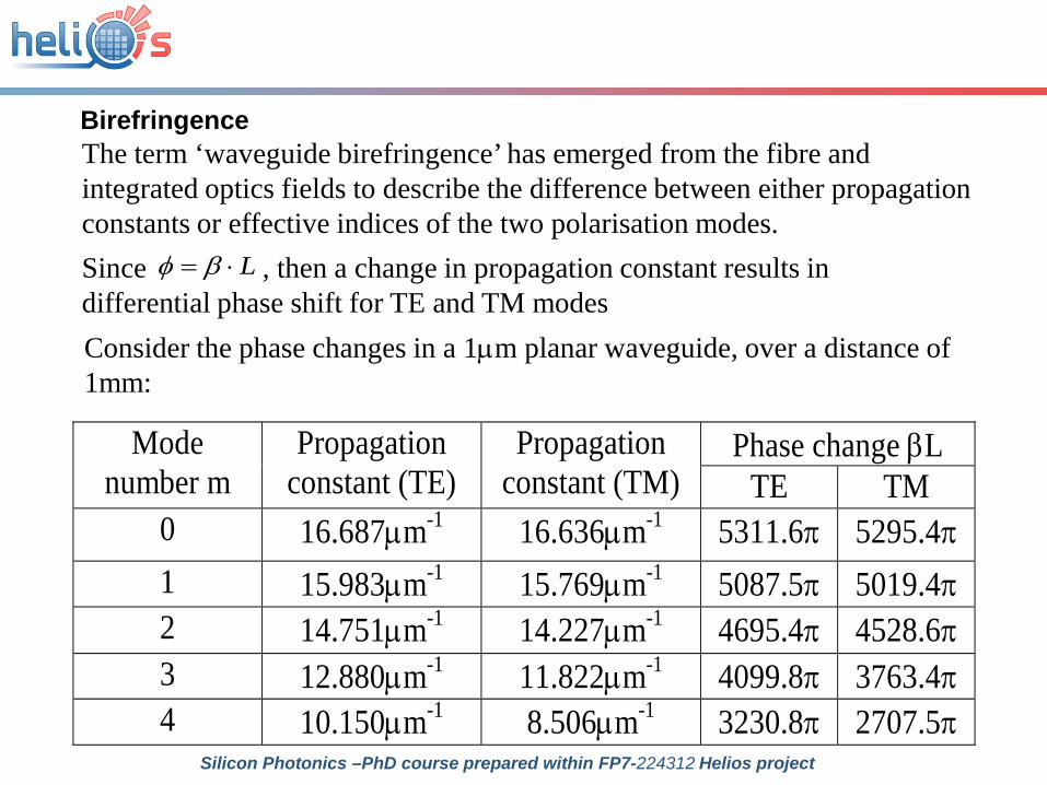
BirefringenceThe term ‘waveguide birefringence’ has emerged from the fibre and integrated optics fields to describe the difference between either propagation constants or effective indices of the two polarisation modes.Since , then a change in propagation constant results in differential phase shift for TE and TM modes
L⋅= βφ
Consider the phase changes in a 1µm planar waveguide, over a distance of 1mm:
Phase change βL Mode number m
Propagation constant (TE)
Propagation constant (TM) TE TM
0 16.687µm-1 16.636µm-1 5311.6π 5295.4π 1 15.983µm-1 15.769µm-1 5087.5π 5019.4π 2 14.751µm-1 14.227µm-1 4695.4π 4528.6π 3 12.880µm-1 11.822µm-1 4099.8π 3763.4π 4 10.150µm-1 8.506µm-1 3230.8π 2707.5π
Silicon Photonics –PhD course prepared within FP7-224312 Helios project

Similarly the waveguide birefringence of rib waveguides can be studied by comparing propagation constants. This is equivalent to studying the effective index, N, because:
wg0Nk=β
where Nwg is the effective index of the propagating rib mode.
Let us consider the effect of waveguide birefringence on a Mach-Zehnder interferometer:
The intensity, I, in the output waveguide is given by the well known interferometer transfer function:
)]cos(1[ 11220 LLII ββ −+=The term (β2L2- β1L1), represents the phase difference between the two arms of the interferometer.
Input waveguide Output waveguide
Arm 1
Arm 2
Silicon Photonics –PhD course prepared within FP7-224312 Helios project
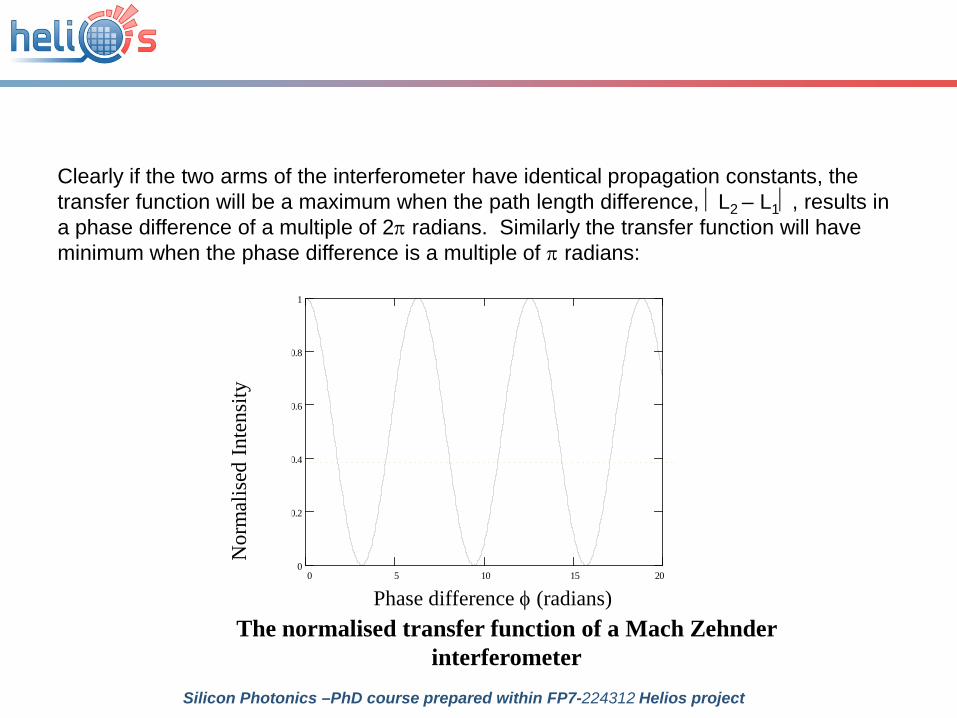
Clearly if the two arms of the interferometer have identical propagation constants, the transfer function will be a maximum when the path length difference, L2 – L1, results in a phase difference of a multiple of 2π radians. Similarly the transfer function will have minimum when the phase difference is a multiple of π radians:
0 5 10 15 200
0.2
0.4
0.6
0.8
1
J( )y2
y2Phase difference φ (radians)
Nor
mal
ised
Inte
nsity
The normalised transfer function of a Mach Zehnder interferometer
Silicon Photonics –PhD course prepared within FP7-224312 Helios project
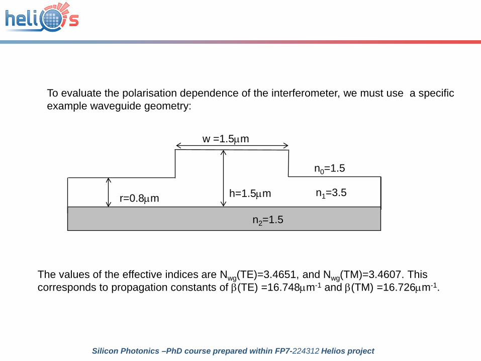
To evaluate the polarisation dependence of the interferometer, we must use a specific example waveguide geometry:
n2=1.5
h=1.5µm n1=3.5
n0=1.5
r=0.8µm
w =1.5µm
The values of the effective indices are Nwg(TE)=3.4651, and Nwg(TM)=3.4607. This corresponds to propagation constants of β(TE) =16.748µm-1 and β(TM) =16.726µm-1.
Silicon Photonics –PhD course prepared within FP7-224312 Helios project
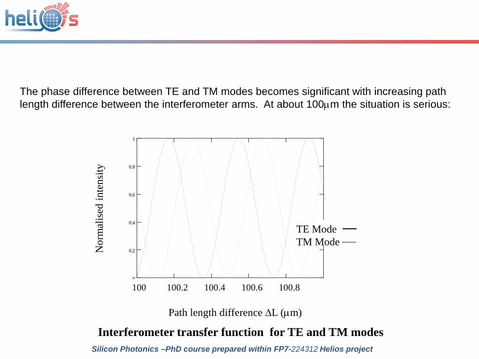
The phase difference between TE and TM modes becomes significant with increasing path length difference between the interferometer arms. At about 100µm the situation is serious:
100 100.2 100.4 100.6 100.80
0.2
0.4
0.6
0.8
1
G( )y
H( )y
y
Path length difference ∆L (µm)
Nor
mal
ised
inte
nsity
Interferometer transfer function for TE and TM modes
TE ModeTM Mode
100 100.2 100.4 100.6 100.8
Silicon Photonics –PhD course prepared within FP7-224312 Helios project
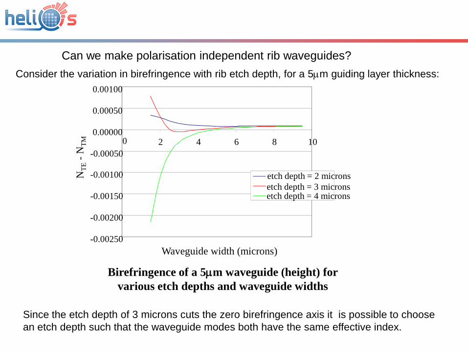
Can we make polarisation independent rib waveguides?Consider the variation in birefringence with rib etch depth, for a 5µm guiding layer thickness:
Since the etch depth of 3 microns cuts the zero birefringence axis it is possible to choose an etch depth such that the waveguide modes both have the same effective index.
-0.00250
-0.00200
-0.00150
-0.00100
-0.00050
0.00000
0.00050
0.00100
0 2 4 6 8 10
Waveguide width (microns)
NTE
-NTM
etch depth = 2 micronsetch depth = 3 micronsetch depth = 4 microns
Birefringence of a 5µm waveguide (height) for various etch depths and waveguide widths
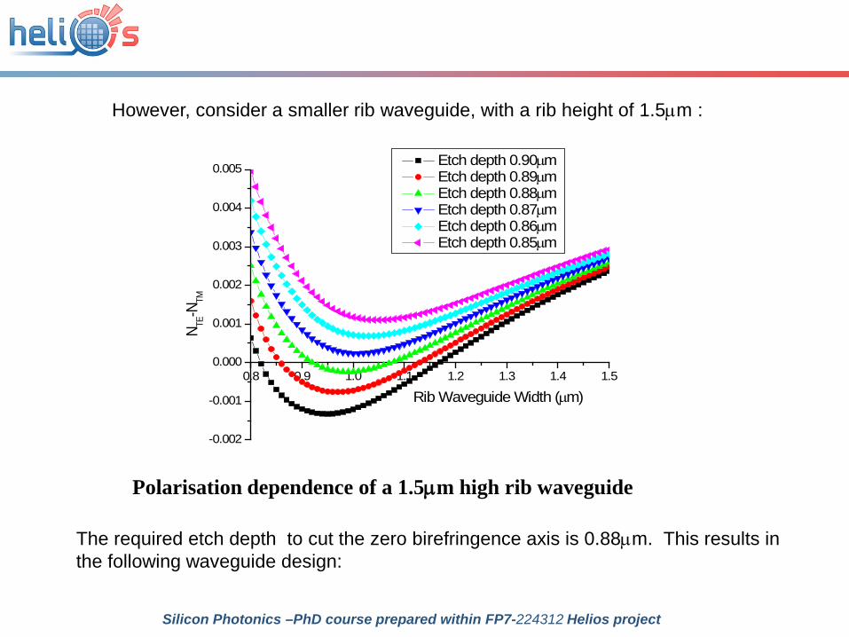
However, consider a smaller rib waveguide, with a rib height of 1.5µm :
The required etch depth to cut the zero birefringence axis is 0.88µm. This results in the following waveguide design:
0.8 0.9 1.0 1.1 1.2 1.3 1.4 1.5
-0.002
-0.001
0.000
0.001
0.002
0.003
0.004
0.005
N TE-N
TM
Rib Waveguide Width (µm)
Etch depth 0.90µm Etch depth 0.89µm Etch depth 0.88µm Etch depth 0.87µm Etch depth 0.86µm Etch depth 0.85µm
Polarisation dependence of a 1.5µm high rib waveguide
Silicon Photonics –PhD course prepared within FP7-224312 Helios project

SiO2
Rib Waveguide Geometry
1.5µm
1.1µm
0.61µm
0.89µm
Such an ‘over-etched’ rib waveguide may violate the single-mode condition
Hence great care is required in the design of the waveguide, particularly at small dimensions
Silicon Photonics –PhD course prepared within FP7-224312 Helios project
Waveguide materialsPlanar waveguidesRib and ridge waveguidesStrip waveguidesLossesPolarisation issuesEffect of stress
Silicon Photonics –PhD course prepared within FP7-224312 Helios project

The effect of stress The semiconductor processing laboratory, together with device packaging, offer numerous opportunities of introducing stress to semiconductor devices and wafers. For optical waveguides this means that the potential exists for stress induced changes in refractive index of the waveguiding layer. This is particularly problematic when the resulting strain field is directional, because this will result in directional changes in the optical properties of the waveguide. This commonly translates to polarisation dependent changes in propagation characteristics and/or losses. Consider an application where stress in an optical system is made a virtue. Such a case is the polarisation maintaining fibre. A directional stress field is deliberately introduced to ensure that orthogonal polarisation modes propagate with significantly different propagation constants. That is to say the fibre is birefringent.
(a) Panda Fibre (b) Bow-tie fibre (c) Elliptical jacket fibre
Three types of high birefringence fibre formed by stress inducing inclusions
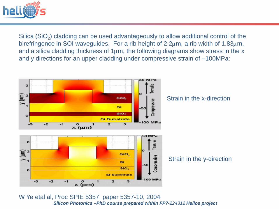
Silica (SiO2) cladding can be used advantageously to allow additional control of the birefringence in SOI waveguides. For a rib height of 2.2µm, a rib width of 1.83µm, and a silica cladding thickness of 1µm, the following diagrams show stress in the x and y directions for an upper cladding under compressive strain of –100MPa:
W Ye etal al, Proc SPIE 5357, paper 5357-10, 2004
Strain in the x-direction
Strain in the y-direction
Silicon Photonics –PhD course prepared within FP7-224312 Helios project
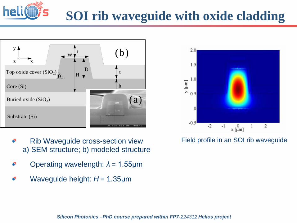
SOI rib waveguide with oxide cladding
Rib Waveguide cross-section view a) SEM structure; b) modeled structure
Operating wavelength: λ = 1.55μm
Waveguide height: H = 1.35μm
W
D
t
t
h
HTop oxide cover (SiO2)
Substrate (Si)
Buried oxide (SiO2)
Core (Si)
y
xz
(a)
(b)
Field profile in an SOI rib waveguide
Silicon Photonics –PhD course prepared within FP7-224312 Helios project
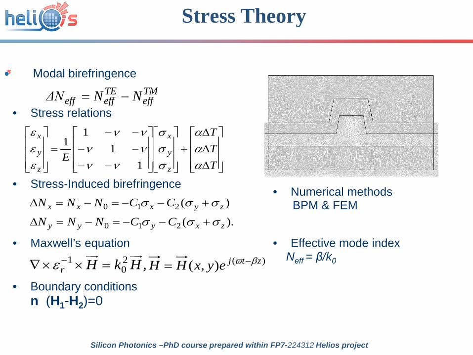
Stress Theory
Modal birefringence
0 1 2
0 1 2
( )
( ).x x x y z
y y y x z
N N N C C
N N N C C
σ σ σ
σ σ σ
∆ = − = − − +
∆ = − = − − +
TMeff
TEeffeff NNΔN −=
• Stress-Induced birefringence
• Stress relations
• Maxwell’s equation1 2
0 ,r H k Hε −∇× × =
∆∆∆
+
−−−−−−
=
TTT
Ez
y
x
z
y
x
ααα
σσσ
νννννν
εεε
11
11
)(),( ztjeyxHH βϖ −=
• Effective mode indexNeff = β/k0
• Numerical methods BPM & FEM
• Boundary conditionsn (H1-H2)=0
Silicon Photonics –PhD course prepared within FP7-224312 Helios project
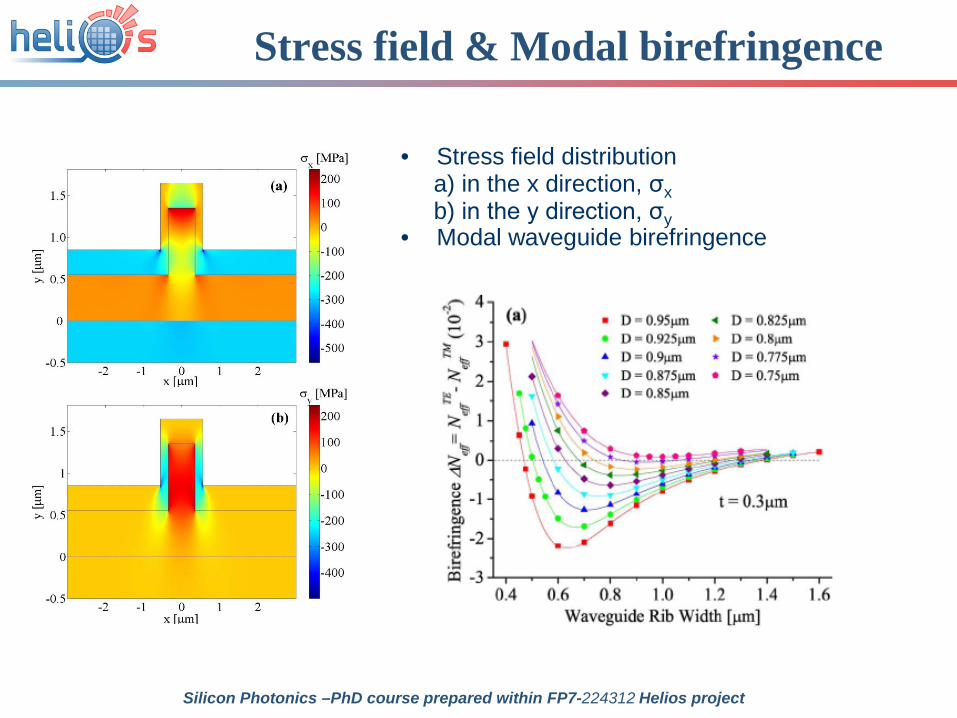
Stress field & Modal birefringence
• Stress field distribution a) in the x direction, σxb) in the y direction, σy
• Modal waveguide birefringence
Silicon Photonics –PhD course prepared within FP7-224312 Helios project

Polarization independent surface
• Zero birefringent surface
• Vertical rib sidewalls θ = 90o
• Zero birefringent condition as a function of waveguide parameters
Silicon Photonics –PhD course prepared within FP7-224312 Helios project
We would like to thank Wiley for giving us a permission to use material from “Silicon Photonics: An Introduction”, G. T. Reed and A. P. Knights, 2004F. Gardes would like to acknowledge the funding from ESPRC “UK Silicon Photonics” grantP. Yang and E. J. Teo contributed to fabrication and characterisation of Si on porous Si waveguidesS. P. Chan and C. E. Png contributed to modelling
Acknowledgements
Silicon Photonics –PhD course prepared within FP7-224312 Helios project