Embed Size (px)
DESCRIPTION
Li - Idaho University - PCB Design With EAGLE (Slides) (2014)
Citation preview

Senior Design Workshop
PCB Design with EAGLE
Dr. Feng Li
Dept. of Electrical & Computer Engineering
University of Idaho
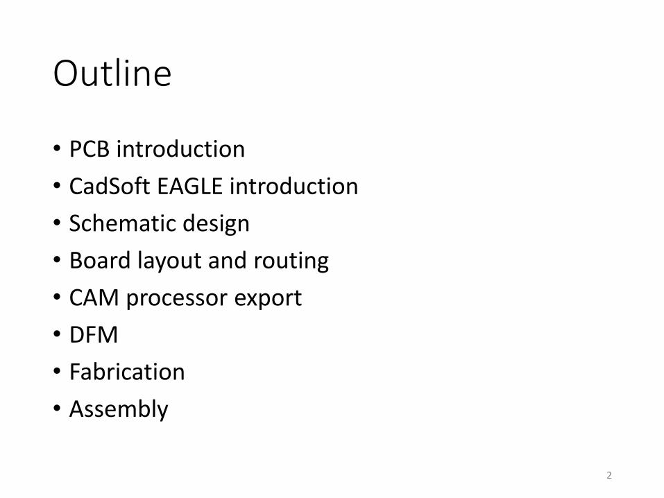
Outline
• PCB introduction
• CadSoft EAGLE introduction
• Schematic design
• Board layout and routing
• CAM processor export
• DFM
• Fabrication
• Assembly
2

What is PCB?
• Printed Circuit Board• Mechanically supports and electrically connects electronic
components using conductive tracks, pads and other features etched from coper sheets laminated onto a non-conductive substrate.
• Two purposes:• A place to mount the component• Provides the means of electrical connection between the
components
• PCBs can be• Single sided (one copper layer)• Double sided (two copper layers)• Multi-layer
3

PCB Terminology – Component Packages• Through-hole
• Soldered to the opposite side of the board
• SMD/SMT (surface mount device/technology)• Soldered in the same side of the board
• Can be mounted on both sides of the PCB
• Smaller than the thru-hole type-smaller & denser PCB
• Some common form factors• 0805 (means 0.08”x0.05”)
• 1206
• 1210
4http://www.pcb.electrosoft-engineering.com/04-articles-custom-system-design-and-pcb/01-printed-circuit-board-concepts/printed-circuit-board-pcb-concepts.html

PCB Terminology
• Pad: a small surface of copper where component will be soldered to the board
• Via: plated hole that allows the current to pass thru the board
• Track (trace): conductive path connecting 2 points (pads, vias)
• Soldermask: a layer of insulating lacquer covering both surfaces of the board to prevent the solder to short-circuit two tracks from different nets.
• Silkscreen (overlay): letters printed on the final board, e.g., solder mask
5

PCB Terminology
6
SMD padsThru-hole pads
Silkscreen
Copper tracks
Soldermask (stop mask)
Via
Thru-hole (full stack) via
1-2 blind via
2-3 buried via
http://www.pcb.electrosoft-engineering.com/04-articles-custom-system-design-and-pcb/01-printed-circuit-board-concepts/printed-circuit-board-pcb-concepts.htmlhttp://en.wikipedia.org/wiki/Via_(electronics)

PCB Process Flow
Schematic
Layout
CAM Gerber output
Production
Assembly
DFM
Function Design
Form factorComponent
library
Design rules
Electronic rules
Routing
EAGLE
FAB house
DIY and/or workshop 7

What is EAGLE?
• Easily Applicable Graphical Layout Editor• Easy to use CAD tool for designing PCBs
• CadSoft
• Consist of three main modules:• Schematic editor
• Layout editor
• Autorouter
• It runs under Windows, Linux, and MacOSX
• It comes with an extensive library of components
8

Three Versions
• EAGLE light• Limitations:
• 1 schematic sheets; • 2 signal layers (top & bottom)• 100x80mm routing area
• It can be used for free
• EAGLE standard• 99 schematic sheets• 4 signal layers• 160x100mmrouting area
• EAGLE Professional: full featured version• Up to 1600x1600mm• Up to 16 routing layer• Up to 999 sheets per schematic
9

Download and Installation
• Current edition: 7.1.0
• http://www.cadsoftusa.com/download-eagle/
• Professional version ( 6.5.0) available in the Senior Design Lab• Contact John Jacksha (J.J.)
• 7.1 and 6.5 may have compatibility issues• Begin with 6.5 light version and use Pro version in lab• Begin with 7.1 light version and order your standard or
professional version
10

Installing Optional Libraries
• SparkFun library• contains footprints for many common devices• helps narrow the choices• https://github.com/sparkfun/SparkFun-Eagle-Libraries• C:\Program Files (x86)\EAGLE-6.5.0\lbr
• Adafruit• http://github.com/adafruit/Adafruit-Eagle-Library• C:\Program Files (x86)\EAGLE-6.5.0\lbr
• Component order• http://www.digikey.com
11

EAGLE User Interface – Control Panel
File manager
Status line
Information window: display what is selected in file manager
Menu bar
12
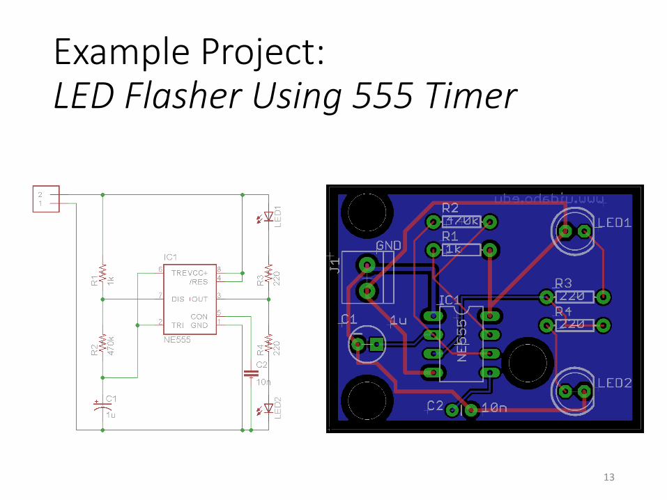
Example Project: LED Flasher Using 555 Timer
13

Creating and Naming a New Project
• File->New->Project (you can name the folder as flasher)
14

Creating a New Schematic
• Right click folder “flasher”->New->Schematic
15

Save and Rename of New Schematic
• [Schematic]File->Save as… (flasher.sch)
• Note: Do not create a
board file yet.
16

Schematic Editor Window
Title Bar
Menu Bar
Toolbar
Parameter toolbar
Command Toolbar
Status Bar
Command Bar
Working Area
17

Schematic Editor Window Command Tools
18
Info – Info on a part Show – Highlight a part, wire, or trace. Very UsefulLayer settings – Change Layers
Name – Name a part Value – Define a value (20 Ohms, etc)
Add – Add a part from the library
Net – Connect component
Group – Define a bunch of parts to a group to move.
Label – Label itemsERC - Electrical Rule Check
Move Rotate
Delete – Delete a part

Finding and Add a Component
• [Schematic] Add
19

Search for a Component
• Enter “*555*” in the Search field
• Find “NE555”
• Click “OK “
20

Drop a Component• Move the cursor toward
the middle of the schematic window
• Click to drop the component
• Press “ESP” key to escape from adding component;
• Click “Cancel” to escape from the adding Window.
• You can delete a Component by clicking “Delete”
21

Add Components – Resistors and Capacitor• SparkFun-Resistors: RESISTORAXIAL-0.3 (x4)
• SparkFun-Capacitors: CAP_POLPTH2
22

Add Component – LED anda Screw Terminal for Power Supply
• Adafruit: LED5MM (search “LED5mm”)
• Adafruit: 1X2-3.5MM (search “terminal”)
23

Rotating and Moving Components
• Rotate
• Move
• Zoom…
24

Connecting the components
• Net
25

Setting Component Values
• Value
26

Electrical Rule Check
• ERC
27

• Use “Show” to show net name
• Search for “capacitor” and find CAP-PTH-SMALL
• Add the capacitor and connect it to Pin5 and the ground
28

29

Net classes• [Schematic]Edit->Net classes
• Can also be done in Layout Editor later
301mil = 0.001inch

Net Classes
• Info
31
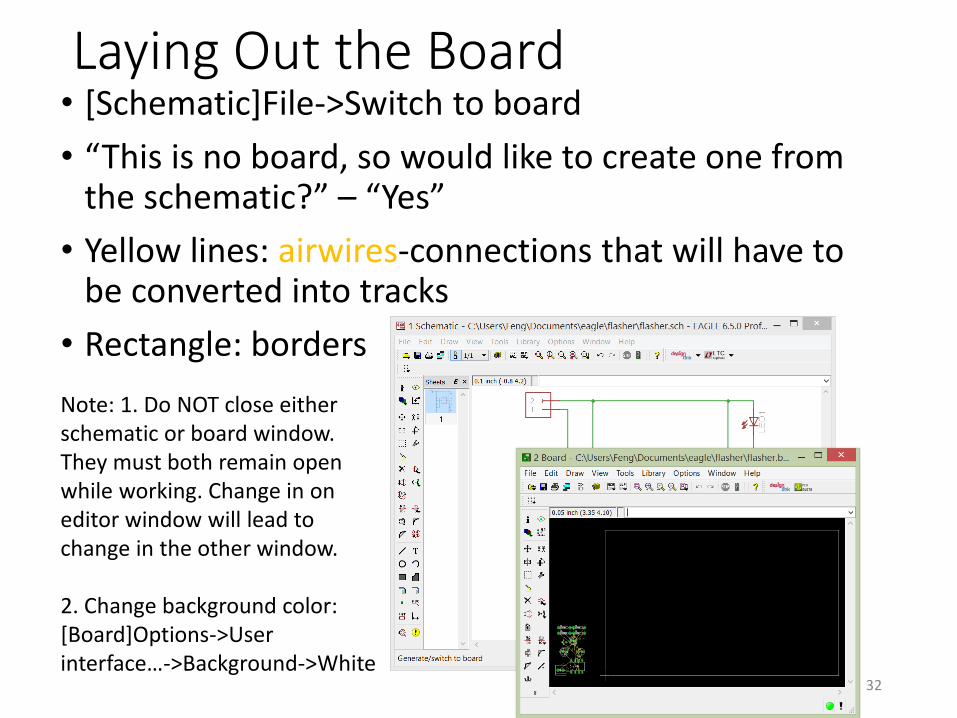
Laying Out the Board• [Schematic]File->Switch to board
• “This is no board, so would like to create one from the schematic?” – “Yes”
• Yellow lines: airwires-connections that will have to be converted into tracks
• Rectangle: borders
32
Note: 1. Do NOT close either schematic or board window. They must both remain open while working. Change in on editor window will lead to change in the other window.
2. Change background color: [Board]Options->User interface…->Background->White

Board ToolsLayer Settings – Change layers
Group – Group multiple components to move at once.
Route – Create a trace (this is the actual wire that carries the electrical signal)
Rectangle – Draw and define a rectangle
Via – Brings a trace from the top layer to the bottom layer
Ratsnest- Calculates the shortest possible airwires and polygons
Design Rule Check – Very Important! More Later
Show – Highlight a trace or part. Useful to see what connects where.
Auto Router – Somewhat unreliable
Polygon – Draw and define a polygon.
Ripup – Remove Traces
Move – Select to Move components
Text – Add text
33

Move
• Move
• Group
• Group move
34

• Move
• Rotate
• Move
• (resizing the board)
• Zoom to fit
35

Ratsnest – calculate the shortest airwires (and polygons)
36

Add Mounting Holes
37

Add Mounting Holes
38

Autorouter
• [Board] Autorouter
39

Board Layout
40

Rip Up the Tracks (Optional)• “Rip up”
• “Group”
• “Ripup: Group”
41

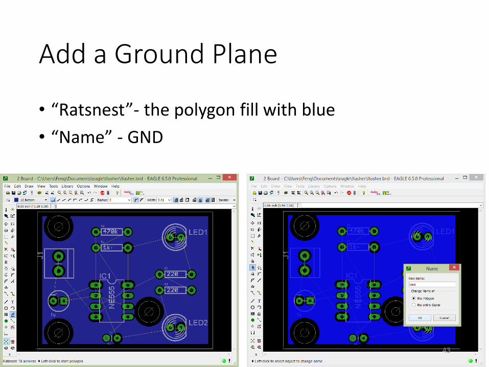
Tweak the Result – Add a Ground Plane
• Polygon – draw a square around the outline of the board
• (Right click the border of the polygon)Properties –Layer: 16 Bottom, Width 0.01
42
Add a Ground Plane
• “Ratsnest”- the polygon fill with blue
• “Name” - GND
43

Add a Ground Plane
• Autorouter
• Ratsnest: Nothing to do!
44

Design Rule Checker
• [Board]DRC
45

CAD Layers
• 1 Top (top tracks)
• 16 Bottom (bottom tracks)
• 17 Pads
• 18 Vias
• 19 Unrouted
• 20 Dimension
• 21 tPlace (top silkscreen)
• 22 bPlace (bottom silkscreen)
• 23 tOrigins
• 24 bOrigins
• 25 tNames
• 26 bNames
• 27 tValues
• 28 bValues
• 44 Drills (for pads (of through hole components) and vias)
• 45 Holes (for mounting holes)
46Note: CAD layer is different from (conductive) layer.

Add Text on the Top (Silkscreen)
• [Board]Layers – Pads, Dimension, tPlace, tOrigins, tNames, tValues
47

Smash – Separate the Text From Devices
• [Board]Smash
• Group
• Smash: Group
48

Change Size
• Change->Size->0.05
49

Change Font
• Change –>Font->Vector
• Group- Change:Group
50

Change Ratio
• Change->Ratio->12
• Group – Change:Group
51

Move Labels
• Move (labels) • Layers – Pads, Dimension, tPlace
52

Add Text to the Top (silkscreen)• Change-Layer-tPlace
• Change-Size-0.05
• Change-Font-Vector
• Change-Ratio-12
53

Add Text to the Top
• Text->GND
54

Add Text to the Bottom
• Layer->Pads, Dimension, bPlace
• Change->layer->bPlace
55

Add Text to the Bottom
• Text – www.uidaho.edu
56

Final Board Layout
57

Gerber Files
• A 2D vector image format
• Universal format and industry standard for PCB fabrication
• TXT files with coordinates that tell the PCB machines to go to location X, Y and do something (drill, expose, etch, print, etc).
• Formats:• RS-274X (Extended Gerber or X-Gerber)
• Human readable ASCII format consisting of a sequence of commands and coordinates
• RS-274D (obsolete)
• Different text files for different layers.
• Generated by the CAM (computer aided manufacturing) processor
58

Typical Gerber File TypesDescription EAGLE (default) EAGLE (Sparkfun) Orcad Protel
Top copper layer (component side)
cmp gtl top gtl
Bottom copper layer (solder side)
sol gbl bot gbl
Top solder mask stc gts smt gts
Bottom solder mask sts gbs smb gbs
Top overlay (silkscreen) plc gto sst gto
Bottom overlay (silkscreen) pls gbo ssb gb0
NC Drill file (coordinate info) drd txt thruhole.tap drl
Note: Extensions are different for different PCB design tools, but information is the same.
EAGLE default CAM job needs to create drill file and gerber files separately. SparkFun CAM job needs only one step.https://github.com/sparkfun/SparkFun_Eagle_Settings/tree/master/camDownload the file sfe-gerb274x.cam, and save to some folder 59

Gerber File Generation – CAM Processor• [Board] File->CAM Processor
• [CAM Processor] File->Open->Job->sfe-gerb274x.cam
60

Gerber File Generation – CAM Processor• [CAM Processor] Process Job
61

Gerber Review, Submit and Order
• Review: verify the CAM output in a Gerber viewer to make sure everything was positioned correctly• Viewplot: http://www.viewplot.com (can be downloaded and
installed• Online viewer: www.gerber-viewer.com
• Design for manufacturability (DFM)(Files upload)• FreeDFM: http://www.freedfm.com
https://www.my4pcb.com/net35/FreeDFMNet/FreeDFMHome.aspx
• Some PCB fab houses• Advanced Circuits http://www.4PCB.com
• quick, reliable, and relatively cheap • $33/board with a week turn around
• Dirty Circuits http://www.dirtycircuits.com
62

Assembly (Soldering)
• Through-hole components • DIY at ECE Senior Design Lab (BEL 216)
• Surface-mount devices• GJL 001 ECE lab (free)
• < 30 components
• Case size > 0402
• Label pin numbers
• Mr. Greg Klemesrud: [email protected]
63

Reference
• Simon Monk, “Make Your Own PCBs with EAGLE: From Schematic Designs to Finished Boards,” McGraw-Hill/TAB Electronics; 1 edition (May 22, 2014)
64
Special Thanks to
• Dr. Michael Santora
• Dr. Steven Beyelein
• Mr. John Jacksha (J. J.)
• Mr. Greg Klemesrud