Embed Size (px)
Citation preview
LLAMAS: Large-Area Microphone
Arrays and Sensing Systems
Josue Sanz-Robinson
A Dissertation
Presented to the Faculty
of Princeton University
in Candidacy for the Degree
of Doctor of Philosophy
Recommended for Acceptance
by the Department of
Electrical Engineering
Adviser: Professor James C. Sturm
May 2016
c© Copyright by Josue Sanz-Robinson, 2016.
All rights reserved.
Abstract
Large-area electronics (LAE) provides a platform to build sensing systems, based
on distributing large numbers of densely spaced sensors over a physically-expansive
space. Due to their flexible, “wallpaper-like” form factor, these systems can be seam-
lessly deployed in everyday spaces. They go beyond just supplying sensor readings,
but rather they aim to transform the wealth of data from these sensors into action-
able inferences about our physical environment. This requires vertically integrated
systems that span the entirety of the signal processing chain, including transducers
and devices, circuits, and signal processing algorithms. To this end we develop hybrid
LAE / CMOS systems, which exploit the complementary strengths of LAE, enabling
spatially distributed sensors, and CMOS ICs, providing computational capacity for
signal processing.
To explore the development of hybrid sensing systems, based on vertical integra-
tion across the signal processing chain, we focus on two main drivers: (1) thin-film
diodes, and (2) microphone arrays for blind source separation:
1. Thin-film diodes are a key building block for many applications, such as RFID
tags or power transfer over non-contact inductive links, which require rectifiers
for AC-to-DC conversion. We developed hybrid amorphous / nanocrystalline
silicon diodes, which are fabricated at low temperatures (<200 ◦C) to be com-
patible with processing on plastic, and have high current densities (5 A/cm 2 at
1 V) and high frequency operation (cutoff frequency of 110 MHz).
2. We designed a system for separating the voices of multiple simultaneous speak-
ers, which can ultimately be fed to a voice-command recognition engine for
controlling electronic systems. On a device level, we developed flexible PVDF
microphones, which were used to create a large-area microphone array. On a
circuit level we developed localized a-Si TFT amplifiers, and a custom CMOS
iii
IC, for system control, sensor readout and digitization. On a signal processing
level we developed an algorithm for blind source separation in a real, reverber-
ant room, based on beamforming and binary masking. It requires no knowledge
about the location of the speakers or microphones. Instead, it uses cluster anal-
ysis techniques to determine the time delays for beamforming; thus, adapting
to the unique acoustic environment of the room.
iv
Acknowledgements
Writing this section was pretty hard. I have to confess it was only slightly less
challenging than trying to explain undersampled microphone reconstruction, mainly
because inputting big matrixes into LATEX is not so user friendly. This section is hard
because a systems Ph.D. involves laughing (in defeat ... ... ... and sometimes vic-
tory), collaborating and learning from so many people that it’s nearly guaranteed I’m
going to forget someone really important. Therefore, by adding some lofty sounding
legalese at this point, I hope you (hereinafter referred to as “THE UNWITTINGLY
FORGOTTEN IN TEXT, BUT NOT IN MIND”) will forgive me and accept my
thanks.
I would like to thank my three incredible thesis advisors. Prof. Jim Sturm for
always providing support and being unfailingly enthusiastic about my research, but
giving me the independence to try out my own ideas and explore my diverse research
interests, even if at times they were risky or far-fetched, or occasionally even resembled
a random walk. I am sure this process will be the most valuable aspect of my time
at Princeton, since it has made me (at least I’d like to think!) much better at solving
complex problems (both in and out of lab). I am also very grateful for you teaching me
that as far as science is concerned, holy cows do not exist (and when in doubt citing
Wronski is not a valid escape maneuver), and that most complex phenomena can be
reduced to a simple and intuitive explanation, once you can cut through the jargon
and actually understand the basics. Prof. Naveen Verma for showing me through
example how a can-do attitude can go a long way, including building systems that
quite frankly initially I thought weren’t possible. The time you so generously spent
debugging circuits with me or even writing code (I still maintain that time series
are column vectors, not row vectors) were some of the most educational parts of my
work. Through your unique multi-disciplinary vision, and by never accepting lack of
knowledge or skills as an acceptable excuse when facing a problem, you have kept
v

me constantly learning, challenged and engaged, and have enabled (your favourite
word!) me to become a far more versatile and adaptable engineer. Prof. Sigurd
Wagner for being the wise Gandalf the Grey, and always having your door open to
listen to any problems ranging from the mundane running of the PECVD to deep
scientific quandaries, and have the uncanny skill to within seconds perfectly visualize
the situation and magically conjure up an action plan. Without all the knowledge
and infrastructure you have built up over decades, this work would not have been
possible.
I would like to thank my thesis readers, Prof. Barry Rand and Prof. Sigurd Wag-
ner for reading through this thesis so carefully and providing much valuable feedback,
despite the tight deadline. I would also like to thank Prof. Kaushik Sengupta for be-
ing on my committee, and being so accommodating when I was tackling the mutually
exclusive schedules problem.
Hatte a special thanks for always being there for me, for being far too selfless
and generous, and for unfailingly looking after my best interests, as well as being
immeasurably fun to spend time with. Thanks for being my trusty spotter both
when flying Quaddie (such a fun activity, right?) and nearly as importantly in life.
Who else could tolerate, and even humour my incoherent and incessant babbling?
Warren, the most sharp, generous and reasonable labmate I could have asked for.
I mean who else could be readily coerced into labeling > 1000 resistors or making
an endless supply of diagrams (without even grimacing)? If I ever have to unclog a
PECVD pipe or require help with any other critical decision you will be at the top
of my shortlist! Bhadri for being the ultimate sensei when I was starting my Ph.D
and providing so many valuable suggestions throughout these years... you taught me
so much about fixing machines and even quite a bit of semiconductor device physics.
Every day when I wake up (hopefully, not too early in the morning) my tastefully
restored espresso machine salutes you! Dylan and Liechao for being excellent col-
vi
laborators, and working with me late into the night calmly and resolutely; however,
tight the impending deadline. Tiffany for being the best lab logistics organizer, al-
ways being there to discuss and troubleshoot any technical problems, and bringing
an invaluable, healthily skeptical and pragmatic voice of reason to the table. Yasmin,
even though I deeply regret failing to convince you about the virtues of free markets,
for bringing great enthusiasm to the lab and always being ready for a lively debate
(in which I am always right!). Hongyang for being excellent to work with on the final
demo; I’m sure you have a great time ahead of you! Levent for being so helpful and
for being the best Powerpoint DJ ever. Janam, Joseph, Ken, Can, Noah, Ting, Yoni,
Amy, Jiun-Yun, Chiao-Ti, Zander, Bahman, Sushobhan, Yifei and Wenzhe for your
great friendship and always being ready to pitch in!
Soumyadeep for giving me solid quantitative-based 360-degrees advice, for being
ready to discuss tech, business or politics with me (especially Mr. Modi), and for
your excellent sense of adventure both culinary (yum, yum... Indian-Chinese) and
otherwise. Herr. Prof. Dr. Alain Plattner (cause I know deep down you’re a Swiss
stickler, even though you like to pretend to be a cool kid) for always being ready to
explore things with me (even Soviet propaganda posters) and being so diplomatic that
you even claim to like some of my most unpalatable espresso experiments ever. Gomas
for playing an indispensable role in completing my still life painting assignments in
high school art class (the paint always inexplicably ended on my body, rather than
the paper). Now, as a professional artist, once again you have come to my rescue
with the fantastic LLAMA illustrations for this thesis.
I would like to thank Pat Watson, Joe Palmer and Bert Harrop for going way
beyond their call of duty. I would have to be an alien with 101 digits to be able to
count on my fingers how many times you came to my rescue in the cleanroom. Prof.
Edgar Choueiri, and his student, Joe Tylka, for helping me ramp up on microphone
vii

measurements and letting me use their anechoic chamber. Josh Spechler for making
the nanowires for the microphones.
Sheila Gunning, Barbara Fruhling, Carolyn Arnesen and Roelie Abdi for doing
such an excellent job of looking after all my administrative needs, including order-
ing stuff from obscure (sometimes only Finnish speaking) suppliers, making sure I
(mostly) filed my paperwork on time and overall shielding me from bureaucracy. I
would also like to thank Colleen Conrad for her very efficient help with thesis paper-
work, with which without you might be reading this page in several months (keeping
fingers crossed until the library accepts this document; I hear they want it printed
on organically-grown vellum from a kangaroo). I would also like to thank Mladenka
Tomasevic from the Davis International Center for her help trying to understand the
infinitely rich and complex world of US immigration law.
Last, but not least, I would like to thank my family. My parents, Jo and Nacho,
who have unconditionally always done everything within their power to help me on
my quests, and are my best allies. Even nowadays I still dutifully listen to your advice
(when I’m not trying to multitask by typing and having a fluid Skype conversation
with you at the same time), although whether I decide it is actionable is another
matter! I even sometimes make sure to get some sunlight, since in your words, “I’m a
tropical creature, prone to vitamin D deficiency.” My brothers, Jethro and Jacob, for
always being up for a good game, conversation or even being my younger (but more
sophisticated) wingman.
viii
Contents
Abstract . . . . . . . . . . . . . . . . . . . . . . . . . . . . . . . . . . . . . iii
Acknowledgements . . . . . . . . . . . . . . . . . . . . . . . . . . . . . . . v
List of Tables . . . . . . . . . . . . . . . . . . . . . . . . . . . . . . . . . . xiv
List of Figures . . . . . . . . . . . . . . . . . . . . . . . . . . . . . . . . . . xv
1 Introduction 1
1.1 Hybrid System Architecture . . . . . . . . . . . . . . . . . . . . . . . 2
1.1.1 Sensors . . . . . . . . . . . . . . . . . . . . . . . . . . . . . . . 3
1.1.2 Powering . . . . . . . . . . . . . . . . . . . . . . . . . . . . . . 4
1.1.3 Computation . . . . . . . . . . . . . . . . . . . . . . . . . . . 4
1.2 Physical System Design . . . . . . . . . . . . . . . . . . . . . . . . . 5
1.3 Thesis Structure . . . . . . . . . . . . . . . . . . . . . . . . . . . . . 8
1.3.1 Part I: High-Frequency Thin-Film Diodes . . . . . . . . . . . 8
1.3.2 Part II: Large-Area Microphone Arrays for Source Separation 9
2 Thin-film Schottky Diodes: Processing and DC Characteristics 11
2.1 Material Selection . . . . . . . . . . . . . . . . . . . . . . . . . . . . . 12
2.1.1 Amorphous Silicon (a-Si) . . . . . . . . . . . . . . . . . . . . . 12
2.1.1.1 Material Structure and Electrical Properties . . . . 13
2.1.1.2 Deposition Conditions . . . . . . . . . . . . . . . . . 15
2.1.2 Nanocrystalline Silicon (nc-Si) . . . . . . . . . . . . . . . . . . 16
ix
2.1.2.1 Material Structure and Electrical Properties . . . . 17
2.1.2.2 Deposition Conditions . . . . . . . . . . . . . . . . . 19
2.2 Schottky Diode Operating Principles . . . . . . . . . . . . . . . . . . 21
2.3 Device Structure . . . . . . . . . . . . . . . . . . . . . . . . . . . . . 22
2.3.1 Amorphous Silicon Diode . . . . . . . . . . . . . . . . . . . . 22
2.3.1.1 Selecting a Metal for the Schottky Junction . . . . . 23
2.3.2 Hybrid a-Si / nc-Si Diode . . . . . . . . . . . . . . . . . . . . 25
2.4 DC Characteristics . . . . . . . . . . . . . . . . . . . . . . . . . . . . 27
2.4.1 DC SPICE Model . . . . . . . . . . . . . . . . . . . . . . . . 27
2.4.2 a-Si Schottky Diode . . . . . . . . . . . . . . . . . . . . . . . . 29
2.4.3 Hybrid a-Si / nc-Si Schottky Diode . . . . . . . . . . . . . . . 30
2.5 Conclusion . . . . . . . . . . . . . . . . . . . . . . . . . . . . . . . . 32
3 Diode AC Characteristics and Thin-film Rectifiers 33
3.1 AC Characteristics . . . . . . . . . . . . . . . . . . . . . . . . . . . . 34
3.1.1 SPICE AC Model and Diode Cutoff Frequency . . . . . . . . 34
3.1.2 a-Si Schottky Diode . . . . . . . . . . . . . . . . . . . . . . . 36
3.1.3 Hybrid a-Si / nc-Si Schottky Diode . . . . . . . . . . . . . . . 37
3.2 Half-Wave Rectifier . . . . . . . . . . . . . . . . . . . . . . . . . . . . 38
3.2.1 Experimental Setup . . . . . . . . . . . . . . . . . . . . . . . 38
3.2.2 DC Voltage Drop . . . . . . . . . . . . . . . . . . . . . . . . . 39
3.2.3 Power Conversion Efficiency . . . . . . . . . . . . . . . . . . . 42
3.3 Conclusion . . . . . . . . . . . . . . . . . . . . . . . . . . . . . . . . . 43
3.4 Acknowledgments . . . . . . . . . . . . . . . . . . . . . . . . . . . . 44
4 System Development: Large-Area Microphone Array for Source
Separation Based on a Hybrid Architecture Exploiting Thin-film
Electronics and CMOS 46
x
4.1 System Design Approach . . . . . . . . . . . . . . . . . . . . . . . . . 47
4.1.1 Basic Concept . . . . . . . . . . . . . . . . . . . . . . . . . . . 48
4.1.2 Reverberance and a Hybrid Approach . . . . . . . . . . . . . . 49
4.2 System Design Details . . . . . . . . . . . . . . . . . . . . . . . . . . 54
4.2.1 Thin-film piezoelectric microphone . . . . . . . . . . . . . . . 55
4.2.2 TFT Amplifiers . . . . . . . . . . . . . . . . . . . . . . . . . . 58
4.2.3 TFT Scanning Circuit and LAE / CMOS Interfaces . . . . . . 59
4.2.4 CMOS IC . . . . . . . . . . . . . . . . . . . . . . . . . . . . . 60
4.2.4.1 Low-Noise Amplifier . . . . . . . . . . . . . . . . . . 61
4.2.4.2 Variable-Gain Amplifier . . . . . . . . . . . . . . . . 62
4.2.4.3 Sample-and-Hold and ADC . . . . . . . . . . . . . . 62
4.2.5 Speech Separation Algorithm . . . . . . . . . . . . . . . . . . 63
4.2.5.1 Calibration . . . . . . . . . . . . . . . . . . . . . . . 64
4.2.5.2 Reconstruction . . . . . . . . . . . . . . . . . . . . . 65
4.3 Prototype Measurements and System Demo . . . . . . . . . . . . . . 68
4.4 Conclusion . . . . . . . . . . . . . . . . . . . . . . . . . . . . . . . . . 70
4.5 Acknowledgments . . . . . . . . . . . . . . . . . . . . . . . . . . . . 70
5 Algorithm Development: Blind Source Separation Using a Large-
Area Microphone Array 75
5.1 Audio Signal Processing: Background Concepts . . . . . . . . . . . . 78
5.1.1 Conventional Delay-and-sum Beamforming . . . . . . . . . . . 78
5.1.2 k-means Cluster Analysis . . . . . . . . . . . . . . . . . . . . . 80
5.1.3 Algorithm Implementation Considerations . . . . . . . . . . . 81
5.2 Algorithm . . . . . . . . . . . . . . . . . . . . . . . . . . . . . . . . . 82
5.2.1 Problem Setup . . . . . . . . . . . . . . . . . . . . . . . . . . 82
5.2.2 Beamforming with Frequency Dependent Time Delays . . . . 83
5.2.3 Binary Mask . . . . . . . . . . . . . . . . . . . . . . . . . . . 84
xi
5.2.4 Time Delay Estimates Based on k-Means Clustering . . . . . 85
5.3 Experimental results . . . . . . . . . . . . . . . . . . . . . . . . . . . 87
5.3.1 Setup Conditions . . . . . . . . . . . . . . . . . . . . . . . . . 87
5.3.2 Time Delay Estimator Performance . . . . . . . . . . . . . . . 88
5.3.3 Overall Algorithm Performance . . . . . . . . . . . . . . . . . 89
5.4 Array Design Considerations . . . . . . . . . . . . . . . . . . . . . . . 93
5.5 Algorithm Improvements . . . . . . . . . . . . . . . . . . . . . . . . . 95
5.6 Conclusion . . . . . . . . . . . . . . . . . . . . . . . . . . . . . . . . . 98
6 Conclusion 99
6.1 Acknowledgements . . . . . . . . . . . . . . . . . . . . . . . . . . . . 100
6.2 Future Work . . . . . . . . . . . . . . . . . . . . . . . . . . . . . . . . 101
6.2.1 Thin-Film Diodes . . . . . . . . . . . . . . . . . . . . . . . . . 101
6.2.2 Flexible Microphones . . . . . . . . . . . . . . . . . . . . . . . 102
6.2.3 Algorithms for Large-Area Microphone Arrays . . . . . . . . . 103
A Thin-Film Diode Fabrication Details
105
A.1 a-Si Schottky Diode . . . . . . . . . . . . . . . . . . . . . . . . . . . 105
A.2 Hybrid a-Si / nc-Si Schottky Diode
. . . . . . . . . . . . . . . . . . . . . . . . . . . . . . . . . . . . . . . 107
B Diode Spice Models 110
B.1 a-Si Diode Spice Model . . . . . . . . . . . . . . . . . . . . . . . . . 110
B.2 Hybrid a-Si / nc-Si Diode SPICE Model. . . . . . . . . . . . . . . . 110
C Large-Area Microphone Arrays Measurements and Experimental
Setup 112
C.1 Measuring the Microphone Frequency Response . . . . . . . . . . . . 112
xii
C.2 Measuring the Sound Pressure Level (SPL) . . . . . . . . . . . . . . 113
C.3 Simulating the Transfer Function Between a Source and a Microphone 114
C.4 Characterizing the Performance of a Source Separation Algorithm . . 115
C.4.1 Signal-to-Interferer Ratio (SIR) . . . . . . . . . . . . . . . . . 115
C.4.2 Perceptual Evaluation of Speech Quality (PESQ) . . . . . . . 116
C.5 PVDF Microphone Fabrication . . . . . . . . . . . . . . . . . . . . . 117
C.6 CMOS Amplifiers for Microphone Prototyping . . . . . . . . . . . . 119
C.6.1 Electret Condenser Microphones . . . . . . . . . . . . . . . . 119
C.6.2 Thin-film, PVDF Microphone . . . . . . . . . . . . . . . . . . 119
C.7 Flexible Implementation of Combined Voice Separation and Gesture
Sensing Sheet . . . . . . . . . . . . . . . . . . . . . . . . . . . . . . . 121
D List of Publications and Patent Disclosures Resulting from this The-
sis
123
D.1 Publications . . . . . . . . . . . . . . . . . . . . . . . . . . . . . . . . 123
D.2 Conferences . . . . . . . . . . . . . . . . . . . . . . . . . . . . . . . . 125
D.3 Patent . . . . . . . . . . . . . . . . . . . . . . . . . . . . . . . . . . . 129
Bibliography 131
xiii
List of Tables
1.1 Exploiting the complementary strengths of CMOS and LAE. . . . . . 3
1.2 Comparison of transistor performance from different technologies. . . 5
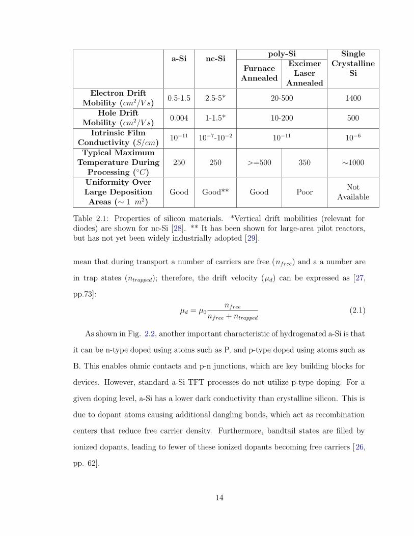
2.1 Properties of silicon materials. . . . . . . . . . . . . . . . . . . . . . 14
2.2 Temperature for interface interactions for metals deposited on a-Si . . 25
2.3 Comparison of parameters for a-Si and hybrid a-Si/nc-Si diode. . . . 30
3.1 Capacitance and cutoff frequency of a-Si and hybrid diodes. . . . . . 39
4.1 Performance summary of the system. . . . . . . . . . . . . . . . . . . 69
5.1 Experimental and Signal Processing Parameters . . . . . . . . . . . . 87
xiv
List of Figures
1.1 Physical design of an LAE sensing system based on laminating sub-
layers with different functionalities. . . . . . . . . . . . . . . . . . . . 6
1.2 Cross section of a non-contact interface used to connect different sub-
layers. . . . . . . . . . . . . . . . . . . . . . . . . . . . . . . . . . . . 7
1.3 Schematic of sub-system required to transmit and receive energy or
power across a non-contact inductive link. . . . . . . . . . . . . . . . 8
2.1 Schematic of the microstructure of different silicon materials. . . . . . 13
2.2 Dark conductivity of a-Si as a function of gas phase ratios. . . . . . . 15
2.3 Schematic of a deposition chamber of the Solarex / Innovate S900
PECVD system. . . . . . . . . . . . . . . . . . . . . . . . . . . . . . . 16
2.4 Cross section of the structure of nc-Si deposited on a substrate. . . . 18
2.5 Dark conductivity of nc-Si as a function of source gas flow ratios. . . 19
2.6 Band diagram of an ideal Schottky diode. . . . . . . . . . . . . . . . 22
2.7 Device structure of a-Si Schottky diode. . . . . . . . . . . . . . . . . 23
2.8 Simplified a-Si diode structure used to rapidly test metals and surface
treatments for the Schottky junction. . . . . . . . . . . . . . . . . . . 25
2.9 Device structure of hybrid a-Si / nc-Si Schottky diode. . . . . . . . . 26
2.10 Device structure of an unsuccessful diode with a metal / nc-Si Schottky
junction. . . . . . . . . . . . . . . . . . . . . . . . . . . . . . . . . . . 26
2.11 SPICE model of Schottky diode with bulk series resistance. . . . . . . 27
xv
2.12 Diode operating regions used to extract parameters for SPICE DC model. 28
2.13 JV curve of a-Si diodes with different intrinsic layer thicknesses. . . 29
2.14 JV characteristics of a hybrid diode and an entirely a-Si Schottky diode. 31
2.15 Degradation of hybrid diode (a) Effect of being exposed to ambient
conditions for 20 days. (b) Effect of being biased at -6 V for 48 hours. 32
3.1 SPICE AC model of Schottky diode. . . . . . . . . . . . . . . . . . . 34
3.2 CV curve of a-Si diodes with different intrinsic layer thicknesses, mea-
sured at 1 MHz. . . . . . . . . . . . . . . . . . . . . . . . . . . . . . 36
3.3 CV curve of hybrid diode, measured at 1 MHz. . . . . . . . . . . . . 38
3.4 Estimating the doping density of nc-Si. . . . . . . . . . . . . . . . . . 38
3.5 Schematic of half-wave rectifier circuit. . . . . . . . . . . . . . . . . . 39
3.6 Half-wave rectifier experimental setup. (a) Mask layout. (b) Photo of
device under test. . . . . . . . . . . . . . . . . . . . . . . . . . . . . . 40
3.7 Half-wave rectifier waveforms from oscilloscope for entirely a-Si diodes
at (a) 1 kHz, and (b) 10 MHz. . . . . . . . . . . . . . . . . . . . . . . 40
3.8 Half-wave rectifier waveforms from oscilloscope for hybrid diodes at (a)
10 MHz, (b) 100 MHz and (c) 200 MHz. . . . . . . . . . . . . . . . . 41
3.9 Output DC voltage as a function of input frequency for both fully a-Si
and hybrid half-wave rectifiers. . . . . . . . . . . . . . . . . . . . . . . 41
3.10 Measuring the power conversion efficiency of a half-wave rectifier with
a hybrid diode. . . . . . . . . . . . . . . . . . . . . . . . . . . . . . . 45
4.1 System of equations for separating two simultaneous sources recorded
with two microphones using previously measured transfer functions. . 48
4.2 Simulated frequency response of perfectly uniform, omnidirectional
microphones and speakers in a (a) reverberant room, and (b) non-
reverberant room. . . . . . . . . . . . . . . . . . . . . . . . . . . . . . 49
xvi
4.3 Reconstruction results for 8-choose-2 pairs of microphones. (a) Simu-
lated in a room without reverberations, directionality, or microphone
process variation; (b) with reverberations and directional microphones. 51
4.4 Simulation parameters for two simultaneous sound sources in a rever-
berant room. . . . . . . . . . . . . . . . . . . . . . . . . . . . . . . . 52
4.5 Proposed structure of the microphone array composed of high SNR
sub-arrays in close proximity to the speaker.. . . . . . . . . . . . . . . 52
4.6 System architecture, combining CMOS ICs and large-area electronics
(LAE). . . . . . . . . . . . . . . . . . . . . . . . . . . . . . . . . . . . 53
4.7 Simulated reconstruction results for the best, median and worst 8-
choose-2 pairs of microphones, and for the eight-channel critically-
sampled sub-array. . . . . . . . . . . . . . . . . . . . . . . . . . . . . 54
4.8 Thin-film PVDF microphone design, including (a) structure, (b) fre-
quency response (measured in an anechoic chamber), and (c) finite
element simulations showing the resonant modes. . . . . . . . . . . . 56
4.9 Frequency response of three “identical” piezopolymer (PVDF) micro-
phones measured in an anechoic chamber. . . . . . . . . . . . . . . . 57
4.10 Polar diagram measured in an anechoic chamber of a PVDF microphone. 57
4.11 (a) Schematic of a two stage TFT amplifier, including (b) measured
noise characteristics of an a-Si TFT , and (c) the simulated tradeoff
between including vs not including a localized TFT amplifier before
long interconnects to a CMOS IC. . . . . . . . . . . . . . . . . . . . . 59
4.12 TFT scanning circuit. . . . . . . . . . . . . . . . . . . . . . . . . . . . 61
4.13 Schematics of the CMOS IC used for readout and digitization. . . . . 62
4.14 Calibration procedure used to find the transfer functions between each
source and microphone. . . . . . . . . . . . . . . . . . . . . . . . . . . 65
xvii
4.15 Algorithm for separating and reconstructing two acoustic sources from
under-sampled microphones in a sub-array using previously calibrated
transfer functions. . . . . . . . . . . . . . . . . . . . . . . . . . . . . . 67
4.16 System Prototype. (a) Micrograph of components: microphone chan-
nel (PVDF microphone and a-Si TFT amplifier), a-Si scanning circuit,
and CMOS readout IC. (b) Testing setup in classroom for full system
demonstration with two simultaneous sources. . . . . . . . . . . . . . 72
4.17 Component-level measurement. . . . . . . . . . . . . . . . . . . . . . 73
4.18 Demonstration of two-source separation and reconstruction for two si-
multaneous wedge-shaped inputs. . . . . . . . . . . . . . . . . . . . . 73
4.19 Demonstration of two-source separation and reconstruction for two si-
multaneous speech signals. . . . . . . . . . . . . . . . . . . . . . . . . 74
5.1 Illustration showing how each microphone in an array receives a signal,
consisting of the sum of the time delayed target and the interferer. . . 79
5.2 Illustration showing how TDOAs can be geometrically calculated for a
linear microphone array. . . . . . . . . . . . . . . . . . . . . . . . . . 79
5.3 Illustration of using k-means to find two clusters. . . . . . . . . . . . 81
5.4 Block diagram of our proposed algorithm. . . . . . . . . . . . . . . . 82
5.5 Experimental room setup (top view) . . . . . . . . . . . . . . . . . . 86
5.6 Microphone sensitivity measured in an anechoic chamber. (a) Omni-
directional electret microphone, (b) LAE microphone. . . . . . . . . . 87
5.7 SIR for time delays extracted from different frames versus the silhou-
ette of the frame for two sources . . . . . . . . . . . . . . . . . . . . . 90
5.8 Comparison of phase for two representative microphones extracted
from white noise and k-means (a) Microphone 4, Source B; (b) Mi-
crophone 12, Source C. . . . . . . . . . . . . . . . . . . . . . . . . . 90
5.9 Separating two sources with an array of electret microphones. . . . . 91
xviii
5.10 Separating two sources with an array of LAE (PVDF) microphones. 92
5.11 Separating four sources with an array of electret microphones . . . . 93
5.12 Separating four sources with an array of LAE (PVDF) microphones. 94
5.13 Algorithm performance as function of the number of microphones. . . 95
5.14 Algorithm performance as function of the spacing between microphones. 96
B.1 Schematic of a-Si diode SPICE model. . . . . . . . . . . . . . . . . . 110
B.2 Schematic of hybrid diode SPICE model. . . . . . . . . . . . . . . . . 111
C.1 Procedure for fabricating a PVDF microphone . . . . . . . . . . . . . 119
C.2 Schematic of amplifier circuit for electret condenser microphone. . . . 120
C.3 Schematic of differential, instrumentation amplifier circuit for PVDF
microphone. . . . . . . . . . . . . . . . . . . . . . . . . . . . . . . . . 120
C.4 Combined gesture sensing and speech separation demo implemented
on a flexible window shade. . . . . . . . . . . . . . . . . . . . . . . . 122
C.5 Flexible gesture sensing sheet attached to the back of the window shade. 122
xix
Chapter 1
Introduction
Large-area electronics (LAE) provides a platform for developing sensing systems with
a flexible, wallpaper-like form factor. It benefits from a wide variety of thin-film
sensors that have already been demonstrated to address a diverse application space.
Using LAE, these sensors can be fabricated in close proximity to each other to enable
sensing with a high spatial resolution, while at the same time sampling over a large
surface area. This makes LAE a compelling technology for measuring, understanding
and interacting with our macroscopic environment. Furthermore, LAE has a flexible
form factor, which is well suited for field deployment.
To harness the power of LAE as a sensing platform, we need to go beyond only
considering the sensors in isolation. Rather we need to develop vertically integrated
architectures that span the entirety of the signal processing chain, encompassing
transducers, circuits and signal processing. From a circuit perspective, key compo-
nents include:
1. Instrumentation circuits, for conditioning the signals and ensuring the integrity
of the data acquired by the sensors.
2. Control circuits, for controlling access and readout from the large number of
sensors involved.
1
3. Digitization circuits, so that the data from the sensors is prepared for digital
signal processing (DSP).
From a signal processing perspective, to benefit from the wealth of data provided
by arrays of spatially distributed sensors, novel algorithms are required. These algo-
rithms play the role of:
1. Enabling systems to interpret and react to complex sensor data.
2. Mitigating the detrimental effects of sensor and thin-film circuit variance caused
by manufacturing and operating over large areas.
3. Enabling systems that can adapt to unpredictable environmental conditions
during deployment.
In the future the widescale adoption of large-area sensing systems will be highly
dependent on attaining low prices per unit area. Due to close alignment in terms of
materials and devices utilized, manufacturing innovations from the display industry
are directly translatable to LAE. Already today when commercially manufacturing
active-matrix liquid crystal displays (AMLCDs), including TFT backplanes, glass
substrates with areas close to 10 m2 are used. The cost of AMLCDs has dropped
from $10,000 USD in the mid-1990s to less than $100 USD today. It is expected that
advances in manufacturing, such as additive printing, will further drive down costs [ 1].
On the basis of these trends in the future we expect LAE to emerge as an economically
viable technology for covering large surfaces, including civil infrastructure, such as
sections of bridges or aircraft wings.
1.1 Hybrid System Architecture
Large-area sensing systems, which are based on thin-film transistors (TFTs) have
been previously demonstrated [2] [3]. Unfortunately, due to their reliance on TFTs
2
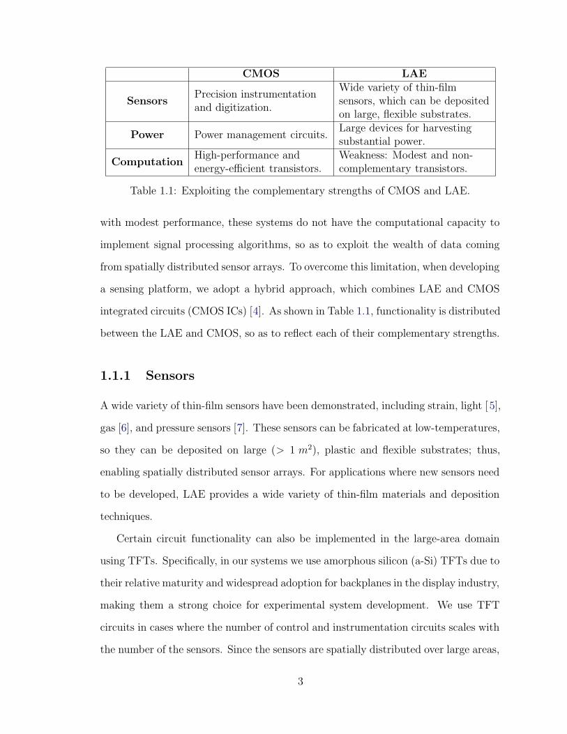
CMOS LAE
SensorsPrecision instrumentationand digitization.
Wide variety of thin-filmsensors, which can be depositedon large, flexible substrates.
Power Power management circuits.Large devices for harvestingsubstantial power.
ComputationHigh-performance andenergy-efficient transistors.
Weakness: Modest and non-complementary transistors.
Table 1.1: Exploiting the complementary strengths of CMOS and LAE.
with modest performance, these systems do not have the computational capacity to
implement signal processing algorithms, so as to exploit the wealth of data coming
from spatially distributed sensor arrays. To overcome this limitation, when developing
a sensing platform, we adopt a hybrid approach, which combines LAE and CMOS
integrated circuits (CMOS ICs) [4]. As shown in Table 1.1, functionality is distributed
between the LAE and CMOS, so as to reflect each of their complementary strengths.
1.1.1 Sensors
A wide variety of thin-film sensors have been demonstrated, including strain, light [ 5],
gas [6], and pressure sensors [7]. These sensors can be fabricated at low-temperatures,
so they can be deposited on large (> 1 m2), plastic and flexible substrates; thus,
enabling spatially distributed sensor arrays. For applications where new sensors need
to be developed, LAE provides a wide variety of thin-film materials and deposition
techniques.
Certain circuit functionality can also be implemented in the large-area domain
using TFTs. Specifically, in our systems we use amorphous silicon (a-Si) TFTs due to
their relative maturity and widespread adoption for backplanes in the display industry,
making them a strong choice for experimental system development. We use TFT
circuits in cases where the number of control and instrumentation circuits scales with
the number of the sensors. Since the sensors are spatially distributed over large areas,
3
the associated control circuits and instrumentation should also be distributed over
large areas to facilitate integration. This is achieved by depositing the TFT circuits
on the same large-area substrate as the sensors. In this way, the number of interfaces
required between the CMOS IC and LAE is reduced. For example, in Chapter 4, large-
area scanning circuits used to sequentially poll the sensors, can be fabricated in the
large-area domain. This reduces the number of interfaces between the CMOS IC and
the LAE, since each individual sensor does not need to be connected directly to the
CMOS IC. On the other hand, in cases where the number of circuits do not scale with
the number of sensors, such as precision instrumentation and ADCs for digitization
of sampled or multiplexed signals from LAE, they are implemented directly on the
CMOS IC, allowing them to benefit from improved transistor performance.
1.1.2 Powering
Due to the large areas available, substantial amounts of energy can be generated using
energy harvesting devices with large physical dimensions, so as to create self-powered
systems. Energy harvesting using large-area solar (a-Si or organic), piezoelectric [ 8]
and thermal devices [9] have been demonstrated. Furthermore, energy storage can
be provided by thin-film lithium ion batteries [10]. The CMOS IC is responsible
for power management, including dynamic control, DC / DC conversion and voltage
regulation.
1.1.3 Computation
Table 1.2 compares a-Si TFTs and a crystalline silicon CMOS transistor. Not only
does the a-Si TFT have ∼ 1000× lower electron mobility and unity gain cutoff fre-
quency (ft) than its Si counterpart, but additionally only NMOS devices are prac-
tically realizable. Therefore, for systems that require significant computational ca-
pacity, so as to implement signal processing algorithms and carryout system control,
4
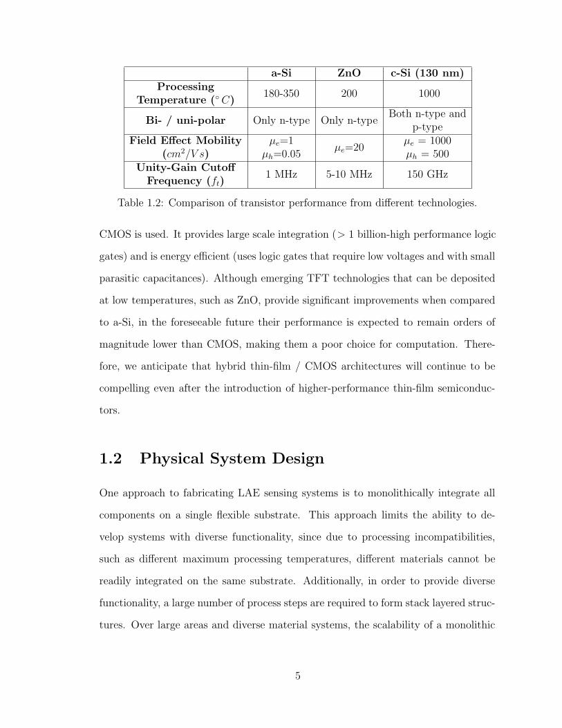
a-Si ZnO c-Si (130 nm)Processing
Temperature (◦ C)180-350 200 1000
Bi- / uni-polar Only n-type Only n-typeBoth n-type and
p-typeField Effect Mobility
(cm2/V s)μe=1
μh=0.05μe=20
μe = 1000μh = 500
Unity-Gain CutoffFrequency (ft)
1 MHz 5-10 MHz 150 GHz
Table 1.2: Comparison of transistor performance from different technologies.
CMOS is used. It provides large scale integration (> 1 billion-high performance logic
gates) and is energy efficient (uses logic gates that require low voltages and with small
parasitic capacitances). Although emerging TFT technologies that can be deposited
at low temperatures, such as ZnO, provide significant improvements when compared
to a-Si, in the foreseeable future their performance is expected to remain orders of
magnitude lower than CMOS, making them a poor choice for computation. There-
fore, we anticipate that hybrid thin-film / CMOS architectures will continue to be
compelling even after the introduction of higher-performance thin-film semiconduc-
tors.
1.2 Physical System Design
One approach to fabricating LAE sensing systems is to monolithically integrate all
components on a single flexible substrate. This approach limits the ability to de-
velop systems with diverse functionality, since due to processing incompatibilities,
such as different maximum processing temperatures, different materials cannot be
readily integrated on the same substrate. Additionally, in order to provide diverse
functionality, a large number of process steps are required to form stack layered struc-
tures. Over large areas and diverse material systems, the scalability of a monolithic
5
approach is questionable, leading to reduced functionality, reduced yield and ensuing
higher production costs.
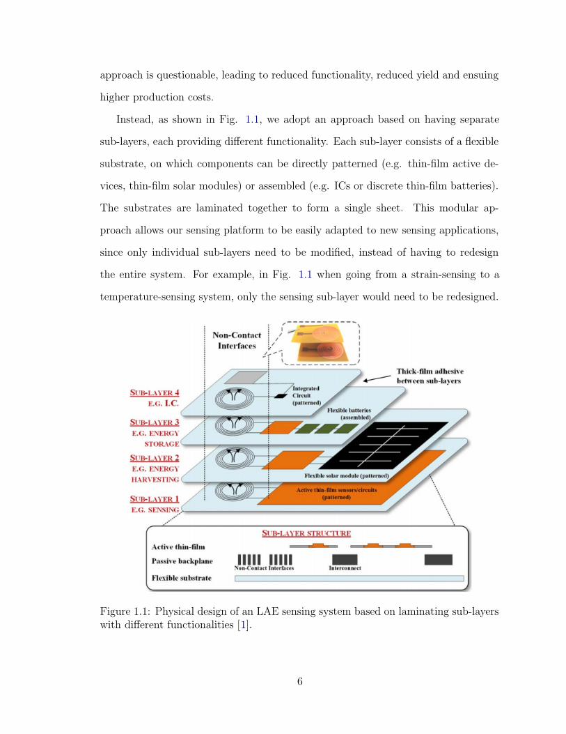
Instead, as shown in Fig. 1.1, we adopt an approach based on having separate
sub-layers, each providing different functionality. Each sub-layer consists of a flexible
substrate, on which components can be directly patterned (e.g. thin-film active de-
vices, thin-film solar modules) or assembled (e.g. ICs or discrete thin-film batteries).
The substrates are laminated together to form a single sheet. This modular ap-
proach allows our sensing platform to be easily adapted to new sensing applications,
since only individual sub-layers need to be modified, instead of having to redesign
the entire system. For example, in Fig. 1.1 when going from a strain-sensing to a
temperature-sensing system, only the sensing sub-layer would need to be redesigned.
Figure 1.1: Physical design of an LAE sensing system based on laminating sub-layerswith different functionalities [1].
6
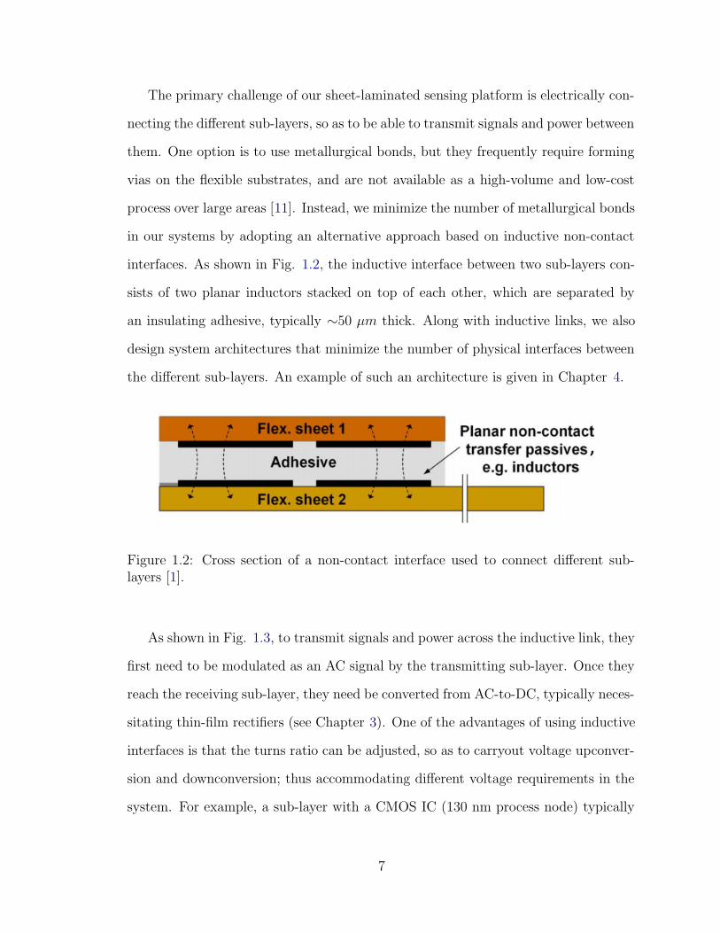
The primary challenge of our sheet-laminated sensing platform is electrically con-
necting the different sub-layers, so as to be able to transmit signals and power between
them. One option is to use metallurgical bonds, but they frequently require forming
vias on the flexible substrates, and are not available as a high-volume and low-cost
process over large areas [11]. Instead, we minimize the number of metallurgical bonds
in our systems by adopting an alternative approach based on inductive non-contact
interfaces. As shown in Fig. 1.2, the inductive interface between two sub-layers con-
sists of two planar inductors stacked on top of each other, which are separated by
an insulating adhesive, typically ∼50 μm thick. Along with inductive links, we also
design system architectures that minimize the number of physical interfaces between
the different sub-layers. An example of such an architecture is given in Chapter 4.
Figure 1.2: Cross section of a non-contact interface used to connect different sub-layers [1].
As shown in Fig. 1.3, to transmit signals and power across the inductive link, they
first need to be modulated as an AC signal by the transmitting sub-layer. Once they
reach the receiving sub-layer, they need be converted from AC-to-DC, typically neces-
sitating thin-film rectifiers (see Chapter 3). One of the advantages of using inductive
interfaces is that the turns ratio can be adjusted, so as to carryout voltage upconver-
sion and downconversion; thus accommodating different voltage requirements in the
system. For example, a sub-layer with a CMOS IC (130 nm process node) typically
7
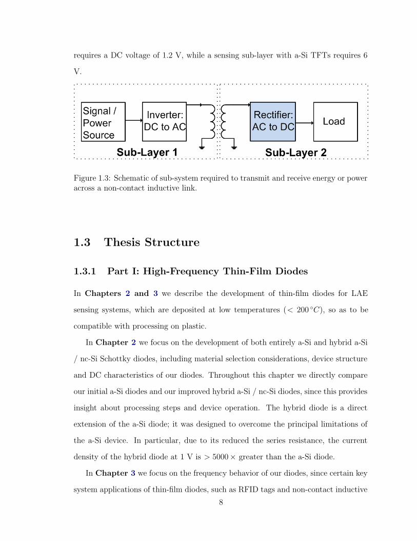
requires a DC voltage of 1.2 V, while a sensing sub-layer with a-Si TFTs requires 6
V.
Figure 1.3: Schematic of sub-system required to transmit and receive energy or poweracross a non-contact inductive link.
1.3 Thesis Structure
1.3.1 Part I: High-Frequency Thin-Film Diodes
In Chapters 2 and 3 we describe the development of thin-film diodes for LAE
sensing systems, which are deposited at low temperatures (< 200 ◦C), so as to be
compatible with processing on plastic.
In Chapter 2 we focus on the development of both entirely a-Si and hybrid a-Si
/ nc-Si Schottky diodes, including material selection considerations, device structure
and DC characteristics of our diodes. Throughout this chapter we directly compare
our initial a-Si diodes and our improved hybrid a-Si / nc-Si diodes, since this provides
insight about processing steps and device operation. The hybrid diode is a direct
extension of the a-Si diode; it was designed to overcome the principal limitations of
the a-Si device. In particular, due to its reduced the series resistance, the current
density of the hybrid diode at 1 V is > 5000× greater than the a-Si diode.
In Chapter 3 we focus on the frequency behavior of our diodes, since certain key
system applications of thin-film diodes, such as RFID tags and non-contact inductive
8
interfaces, require diodes that can operate at high frequencies. First we measure the
capacitance-voltage characteristics of both the a-Si and hybrid diode, so as to create a
SPICE model of each diode. Afterwards we develop a rectifier based on these diodes,
which allows us to confirm the validity of SPICE model. Due to its high current
density and associated high cutoff frequency, the rectifier based on the hybrid diode
can carry out AC-to-DC conversion at frequencies up to 100 MHz, while the a-Si
diode fails at frequencies great than 1 MHz. To evaluate the hybrid diode for power
related applications, we also characterize its power conversion efficiency at different
frequencies.
1.3.2 Part II: Large-Area Microphone Arrays for Source Sep-
aration
In Chapters 4 and 5 we develop a hybrid system for separating independent voice
commands from multiple simultaneous speakers, based on leveraging the spatial fil-
tering capability of a large-area microphone array.
Chapter 4 focuses on the hardware design and a preliminary algorithm for this
system. In the large-area domain, each channel consists of a thin-film transducer
formed from PVDF, a piezopolymer, and a localized amplifier composed of a-Si TFTs.
Each channel is sequentially sampled by a TFT scanning circuit, so as to reduce the
number of interfaces between the LAE and CMOS IC. In the CMOS domain, the
channels are digitized to prepare them for digital signal processing. A reconstruction
algorithm is proposed, which exploits the measured transfer function between each
speaker and microphone, to separate two simultaneous speakers. The algorithm over-
comes (1) sampling-rate limitations of the scanning circuits, and (2) sensitivities to
microphone placement and directionality.
Chapter 5 focuses on the development of a novel blind source separation al-
gorithm, which requires no prior information about the location of the speakers or
9
microphones. We initially describe the mathematical principles of our algorithm,
which consists of a beamforming stage, followed by a binary mask stage for further
interference cancellation. There is an additional stage that uses cluster analysis to es-
timate time delays for beamforming from the audio signal with simultaneous sources.
Subsequently we test the performance of our algorithm in a reverberant room with
up to four simultaneous speakers, using an array of commercial electret microphones
and an array of thin-film (PVDF) microphones.
10
Chapter 2
Thin-film Schottky Diodes:
Processing and DC Characteristics
Diodes are a key building block when developing circuits. Thin-film diodes are crucial
for many large-area applications, such as RFID tags [12][13] or power transfer over
non-contact inductive links [14], which require rectifiers for AC-to-DC power conver-
sion. They can also be integrated with TFTs when designing large-area circuits, so
as to overcome some of TFT’s performance limitations. For example, they can be
incorporated into TFT-based digital logic circuits, such as scanning circuits which
sequentially poll sensors, to enable the output of the circuit to provide a full-voltage
swing; thus, compensating for the lack of complementary p-type TFTs [15]. Thin-film
diodes also play an important role in LAE power systems, where, for instance, they
can be used as blocking diodes to prevent a thin-film battery from leaking current
into a solar cell under low illumination conditions [16].
These applications require diodes with no p-type doping (for compatibility with
a-Si TFT fabrication), high forward current density (and associated low voltage drop
across the diode), low reverse leakage current (and associated high ON-to-OFF current
ratio), and are capable of withstanding large reverse bias voltages (e.g. <-8 V, so as to
11
be compatible with typical a-Si TFT operating voltages). To meet these requirements
in this chapter we describe an entirely a-Si Schottky diode and a hybrid a-Si / nc-Si
Schottky, which further improves upon the entirely a-Si diode. Section 2.1 looks at
the material structure, electrical properties and deposition techniques for a-Si and
nc-Si. Section 2.2 reviews the operating principles of Schottky diodes. Section 2.3
describes the device structure and processing considerations for both the a-Si and
hybrid diodes. Finally, Section 2.4 characterizes the DC behavior of both diodes and
explores how this is affected by the device structure. This chapter expands upon the
work described in References [17] and [18].
2.1 Material Selection
2.1.1 Amorphous Silicon (a-Si)
Amorphous silicon is a strong candidate for developing diodes for LAE systems, which
require high device yield and adequate stability. This stems from a-Si being a mature,
low-cost per unit area (when compared to crystalline silicon processing) and proven
technology, which has been shown to have good yields and uniformity over large areas
(∼ 1 m2), even when deposited at low temperatures. This has led to its widescale
industrial adoption, making it the mostly widely used material for manufacturing
display backplanes, which have a-Si TFTs on glass in each pixel [19]. It is also
extensively used for industrially manufacturing thin-film solar cells and photosensors
for imaging applications [20]. It has been demonstrated in a volume manufacturing
context that a-Si TFTs can be readily integrated with diodes to enhance circuit
functionality [21]. Furthermore, it has been shown that viable Schottky barriers can
be formed with a-Si, making Schottky diodes a strong candidate for developing low-
voltage drop diodes [22][23][24].
12
2.1.1.1 Material Structure and Electrical Properties
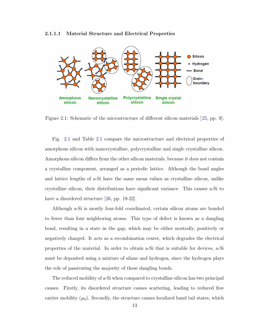
Figure 2.1: Schematic of the microstructure of different silicon materials [25, pp. 9].
Fig. 2.1 and Table 2.1 compare the microstructure and electrical properties of
amorphous silicon with nanocrystalline, polycrystalline and single crystalline silicon.
Amorphous silicon differs from the other silicon materials, because it does not contain
a crystalline component, arranged as a periodic lattice. Although the bond angles
and lattice lengths of a-Si have the same mean values as crystalline silicon, unlike
crystalline silicon, their distributions have significant variance. This causes a-Si to
have a disordered structure [26, pp. 18-22].
Although a-Si is mostly four-fold coordinated, certain silicon atoms are bonded
to fewer than four neighboring atoms. This type of defect is known as a dangling
bond, resulting in a state in the gap, which may be either neutrally, positively or
negatively charged. It acts as a recombination center, which degrades the electrical
properties of the material. In order to obtain a-Si that is suitable for devices, a-Si
must be deposited using a mixture of silane and hydrogen, since the hydrogen plays
the role of passivating the majority of these dangling bonds.
The reduced mobility of a-Si when compared to crystalline silicon has two principal
causes. Firstly, its disordered structure causes scattering, leading to reduced free
carrier mobility (μ0). Secondly, the structure causes localized band tail states, which
13
a-Si nc-Sipoly-Si Single
CrystallineSi
FurnaceAnnealed
ExcimerLaser
AnnealedElectron Drift
Mobility (cm2/V s)0.5-1.5 2.5-5* 20-500 1400
Hole DriftMobility (cm2/V s)
0.004 1-1.5* 10-200 500
Intrinsic FilmConductivity (S/cm)
10−11 10−7-10−2 10−11 10−6
Typical MaximumTemperature During
Processing (◦C)250 250 >=500 350 ∼1000
Uniformity OverLarge DepositionAreas (∼ 1 m2)
Good Good** Good PoorNot
Available
Table 2.1: Properties of silicon materials. *Vertical drift mobilities (relevant fordiodes) are shown for nc-Si [28]. ** It has been shown for large-area pilot reactors,but has not yet been widely industrially adopted [29].
mean that during transport a number of carriers are free (nfree) and a a number are
in trap states (ntrapped); therefore, the drift velocity (μd) can be expressed as [27,
pp.73]:
μd = μ0nfree
nfree + ntrapped
(2.1)
As shown in Fig. 2.2, another important characteristic of hydrogenated a-Si is that
it can be n-type doped using atoms such as P, and p-type doped using atoms such as
B. This enables ohmic contacts and p-n junctions, which are key building blocks for
devices. However, standard a-Si TFT processes do not utilize p-type doping. For a
given doping level, a-Si has a lower dark conductivity than crystalline silicon. This is
due to dopant atoms causing additional dangling bonds, which act as recombination
centers that reduce free carrier density. Furthermore, bandtail states are filled by
ionized dopants, leading to fewer of these ionized dopants becoming free carriers [26,
pp. 62].
14
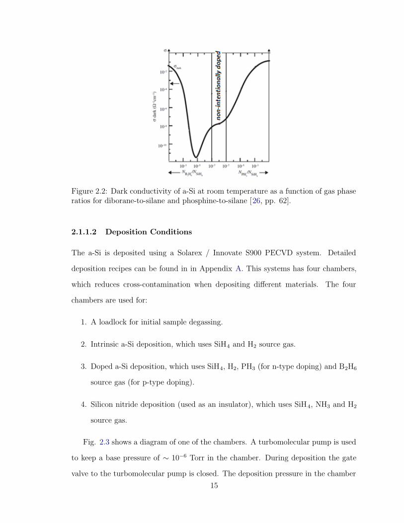
Figure 2.2: Dark conductivity of a-Si at room temperature as a function of gas phaseratios for diborane-to-silane and phosphine-to-silane [26, pp. 62].
2.1.1.2 Deposition Conditions
The a-Si is deposited using a Solarex / Innovate S900 PECVD system. Detailed
deposition recipes can be found in in Appendix A. This systems has four chambers,
which reduces cross-contamination when depositing different materials. The four
chambers are used for:
1. A loadlock for initial sample degassing.
2. Intrinsic a-Si deposition, which uses SiH4 and H2 source gas.
3. Doped a-Si deposition, which uses SiH4, H2, PH3 (for n-type doping) and B2H6
source gas (for p-type doping).
4. Silicon nitride deposition (used as an insulator), which uses SiH4, NH3 and H2
source gas.
Fig. 2.3 shows a diagram of one of the chambers. A turbomolecular pump is used
to keep a base pressure of ∼ 10−6 Torr in the chamber. During deposition the gate
valve to the turbomolecular pump is closed. The deposition pressure in the chamber
15
Figure 2.3: Schematic of a deposition chamber of the Solarex / Innovate S900 PECVDsystem [30, pp. 14].
is set by inputting a constant gas flow into the chamber and controlling the process
valve, which is a PID-controlled butterfly valve.
A plasma is created by using an RF generator at 13.56 MHz to apply voltage
between the cathode, and the grounded top and bottom anode. The reactive gases
diffuse through holes in the cathode and reach the substrate, which is in contact with
the top anode. The plasma plays the role of providing energy to decompose the silane
and other sources, enabling us to deposit a-Si at low temperatures (typically between
180 ◦C to 250 ◦C).
2.1.2 Nanocrystalline Silicon (nc-Si)
Nano-crystalline silicon (nc-Si), also synonymously referred to as microcrystalline (uc-
Si), is a compelling alternative to a-Si for developing TFTs with higher mobilities and
diodes for large-area applications. This is due to its favorable electrical properties,
as shown in Table 2.1. In particular it has a higher mobility (both electron and hole)
and improved doping efficiency when compared to a-Si, enabling it to achieve higher
16
dark current conductivities. This makes it a strong candidate for developing diodes
with higher current densities.
Furthermore, from a large-area manufacturing perspective it is also a strong can-
didate, since it can be deposited using standard a-Si PECVD equipment, without
requiring significant modifications to the equipment. Additionally, it can also be de-
posited at low temperatures (∼ 180◦C ), making it compatible with plastic substrates
for applications that require a flexible form factor. This is a distinct advantage over
polycrystalline silicon, which has a higher mobility than nc-Si, but typically requires
a more complex or higher temperature deposition process, such as furnace or laser
annealing [31].
2.1.2.1 Material Structure and Electrical Properties
The improved electrical properties of nc-Si when compared to a-Si, can be attributed
to nc-Si having a partially crystalline composition. As shown in Fig. 2.1, unlike
polycrystalline and single crystalline silicon, it is not formed exclusively of a crystalline
component. Instead, it consists of mixture of three regions: (1) polycrystalline grains;
(2) disordered, amorphous regions, and (3) voids. The presence of both polycrystalline
and amorphous regions causes it to display electrical properties that lie in between
a-Si and polycrystalline silicon. The proportion of these different components is
strongly dependent on deposition condition. For a given sample, grain sizes vary
widely, typically ranging from several nanometers to more than a micron diameter.
Figure 2.4 shows how the structure of nc-Si varies widely depending on deposition
conditions and thickness. When the deposition initiates, an a-Si incubation region
is formed on top of the substrate, whose thickness depends on the substrate used
and the processing parameters. As the deposition continues, this is followed by a
gradual transition from a-Si to nc-Si. This is caused by the nucleation of crystallites,
which as the growth continues coalesce with each other to form a columnar structure.
17
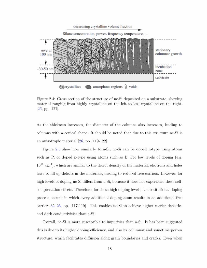
Figure 2.4: Cross section of the structure of nc-Si deposited on a substrate, showingmaterial ranging from highly crystalline on the left to less crystalline on the right.[26, pp. 121].
As the thickness increases, the diameter of the columns also increases, leading to
columns with a conical shape. It should be noted that due to this structure nc-Si is
an anisotropic material [26, pp. 119-122].
Figure 2.5 show how similarly to a-Si, nc-Si can be doped n-type using atoms
such as P, or doped p-type using atoms such as B. For low levels of doping (e.g.
1016 cm3), which are similar to the defect density of the material, electrons and holes
have to fill up defects in the materials, leading to reduced free carriers. However, for
high levels of doping nc-Si differs from a-Si, because it does not experience these self-
compensation effects. Therefore, for these high doping levels, a substitutional doping
process occurs, in which every additional doping atom results in an additional free
carrier [32][26, pp. 117-119]. This enables nc-Si to achieve higher carrier densities
and dark conductivities than a-Si.
Overall, nc-Si is more susceptible to impurities than a-Si. It has been suggested
this is due to its higher doping efficiency, and also its columnar and sometime porous
structure, which facilitates diffusion along grain boundaries and cracks. Even when
18
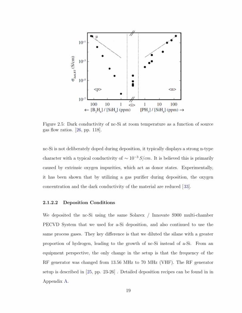
Figure 2.5: Dark conductivity of nc-Si at room temperature as a function of sourcegas flow ratios. [26, pp. 118].
nc-Si is not deliberately doped during deposition, it typically displays a strong n-type
character with a typical conductivity of ∼ 10−3 S/cm. It is believed this is primarily
caused by extrinsic oxygen impurities, which act as donor states. Experimentally,
it has been shown that by utilizing a gas purifier during deposition, the oxygen
concentration and the dark conductivity of the material are reduced [33].
2.1.2.2 Deposition Conditions
We deposited the nc-Si using the same Solarex / Innovate S900 multi-chamber
PECVD System that we used for a-Si deposition, and also continued to use the
same process gases. They key difference is that we diluted the silane with a greater
proportion of hydrogen, leading to the growth of nc-Si instead of a-Si. From an
equipment perspective, the only change in the setup is that the frequency of the
RF generator was changed from 13.56 MHz to 70 MHz (VHF). The RF generator
setup is described in [25, pp. 23-26] . Detailed deposition recipes can be found in in
Appendix A.
19
The amount of dilution the silane has undergone can be characterized using the
silane concentration, given by:
SC =SiH4
SiH4 + H2
(2.2)
e.g. the ratio between the silane gas flow rate entering the process chamber and the
total gas flow rate. The transition from fully a-Si to low quality nc-Si (a material with
a low crystalline fraction) occurs at a silane concentration of 6 % to 9 %. To obtain
a high quality material with a large crystalline fraction, such as required for devices,
a silane concentration of 2 % to 6 % is typically reported [34]. It has been suggested
that the low silane concentration required for nc-Si growth can be explained using a
selective etching model. In this model a-Si and nc-Si are deposited simultaneously,
and chemically etched by atomic hydrogen. Since the a-Si has a higher defect density
and more strained bonds than nc-Si, it is more readily etched than the nc-Si; thus,
nc-Si growth is promoted when more hydrogen atoms reach the surface [35].
Instead of depositing at a frequency of 13.56 MHz, it is preferable to use a VHF
frequency, since it increases the deposition rate and crystallinity. The higher growth
rate is caused by improved gas dissociation in the bulk of the plasma and reduced
thickness of the plasma sheath, which allow more radicals to reach the surface of
the growing film. It has been suggested that the improved crystallinity can also be
explained by a selective etching model, in which at higher frequencies the preferential
etching of a-Si over nc-Si is enhanced. We specifically chose a deposition frequency
of 70 MHz, because prior work shows it provides good thickness uniformity when
compared to a higher frequency, such as 120 MHz, even though this does come at a
cost of slightly reduced crystallinity [25, pp. 39-40].
It should be stressed that the microstructure obtained does not depend exclusively
on the silane concentration or frequency. Rather there is an interdependence of tem-
20
perature, pressure, power density, silane concentration and reactor design. Therefore,
different combinations of these deposition parameters can result in the same mi-
crostructure [35]. When optimizing a recipe not only does nc-Si material quality have
to be considered, but also a high deposition rate and good uniformity over the entirety
of the substrate is required.
2.2 Schottky Diode Operating Principles
When a metal and a semiconductor are brought into contact with each other, assuming
that the metal (φM ) has a work function that is greater than the semiconductor work
function (φS), a Schottky junction is formed, as shown in Fig. 2.6. Before coming
into contact, for two materials with the same vacuum level (no electric field between
them), the Fermi level in the semiconductor is above the metal. Once in contact,
to maintain thermal equilibrium, the Fermi levels must match. This causes a flow
of electrons from the semiconductor to lower energy states in the metal, resulting in
the formation of a space charge region in the semiconductor composed of positively
charged donor atoms, which lowers the energy levels of the semiconductor with respect
to those of the metal. The Schottky barrier height is given by φB = φM − X , while
the built-in barrier is given by φi = φM − φS.
When a positive voltage (VA) is applied to the metal with respect to the semicon-
ductor, φB remains constant, while φi is reduced. This allows electrons to cross more
easily from the semiconductor to the metal, resulting in a current flow. This current
density can be modelled by
J = J0
[
exp
(qVA
nkT
)
− 1
]
(2.3)
where n is the ideality factor, J0 is the reverse saturation current, k is the Boltzmann
constant and T is the temperature.
21
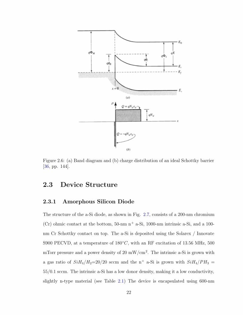
Figure 2.6: (a) Band diagram and (b) charge distribution of an ideal Schottky barrier[36, pp. 144].
2.3 Device Structure
2.3.1 Amorphous Silicon Diode
The structure of the a-Si diode, as shown in Fig. 2.7, consists of a 200-nm chromium
(Cr) ohmic contact at the bottom, 50-nm n+ a-Si, 1000-nm intrinsic a-Si, and a 100-
nm Cr Schottky contact on top. The a-Si is deposited using the Solarex / Innovate
S900 PECVD, at a temperature of 180◦C, with an RF excitation of 13.56 MHz, 500
mTorr pressure and a power density of 20 mW/cm2. The intrinsic a-Si is grown with
a gas ratio of SiH4/H2=20/20 sccm and the n+ a-Si is grown with SiH4/PH3 =
55/0.1 sccm. The intrinsic a-Si has a low donor density, making it a low conductivity,
slightly n-type material (see Table 2.1) The device is encapsulated using 600-nm
22
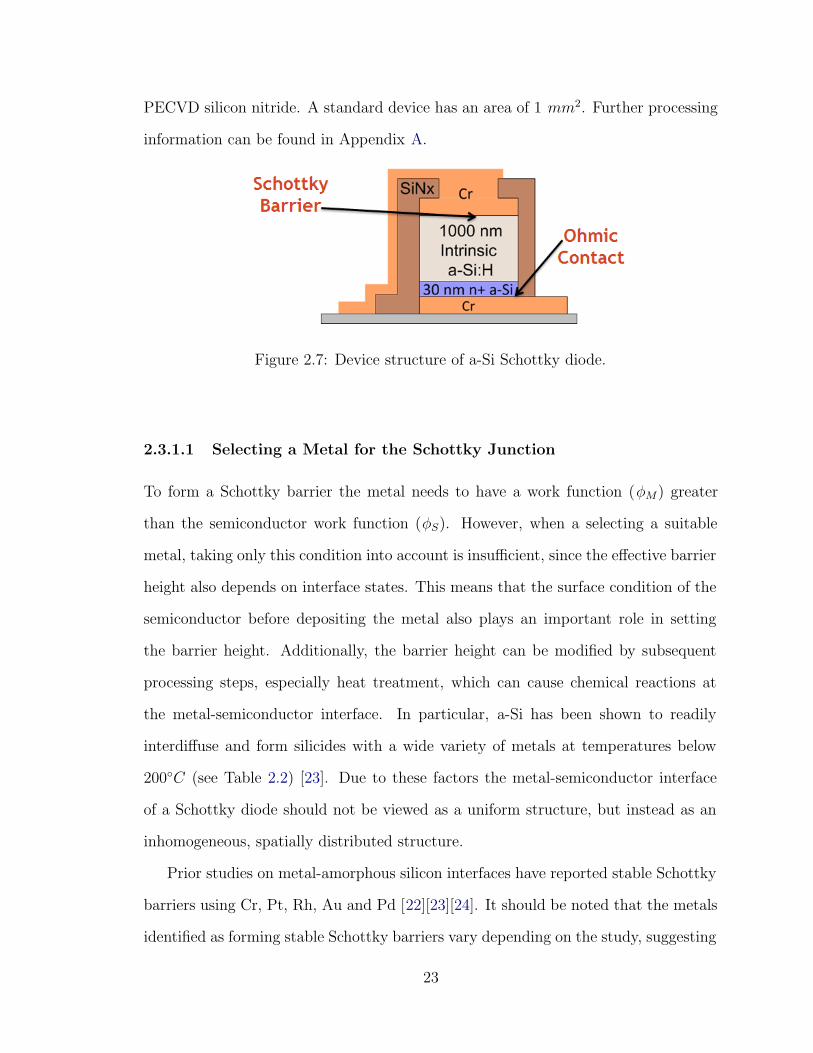
PECVD silicon nitride. A standard device has an area of 1 mm2. Further processing
information can be found in Appendix A.
Figure 2.7: Device structure of a-Si Schottky diode.
2.3.1.1 Selecting a Metal for the Schottky Junction
To form a Schottky barrier the metal needs to have a work function (φM) greater
than the semiconductor work function (φS). However, when a selecting a suitable
metal, taking only this condition into account is insufficient, since the effective barrier
height also depends on interface states. This means that the surface condition of the
semiconductor before depositing the metal also plays an important role in setting
the barrier height. Additionally, the barrier height can be modified by subsequent
processing steps, especially heat treatment, which can cause chemical reactions at
the metal-semiconductor interface. In particular, a-Si has been shown to readily
interdiffuse and form silicides with a wide variety of metals at temperatures below
200◦C (see Table 2.2) [23]. Due to these factors the metal-semiconductor interface
of a Schottky diode should not be viewed as a uniform structure, but instead as an
inhomogeneous, spatially distributed structure.
Prior studies on metal-amorphous silicon interfaces have reported stable Schottky
barriers using Cr, Pt, Rh, Au and Pd [22][23][24]. It should be noted that the metals
identified as forming stable Schottky barriers vary depending on the study, suggesting
23
that the choice of metal is heavily dependent on device processing. For example,
[23][24] reported a satisfactory Schottky barrier with Au, while [22] did not obtain
satisfactory results with this same metal. For our diodes we identified Cr as a good
candidate for our Schottky contact for the following reasons:
1. For deposition over large-areas, it is low cost when compared to many other
metals (e.g. Au, Pt and Pd).
2. We already use Cr for metal contacts (gates and source / drain) for our a-
Si TFTs, so this facilitates integrating our Schottky diodes with TFTs when
developing circuits for LAE systems.
3. Some studies have reported higher current densities for Cr than other Schottky
barrier metals [22].
4. As shown in Table 2.2, higher temperature is required for Cr to react with a-Si
than for other metals. This suggests the metal-semiconductor surface will ex-
perience fewer structural changes during processing or during operation (where
current flowing though the diode could cause heating), leading to a possibly
more stable device.
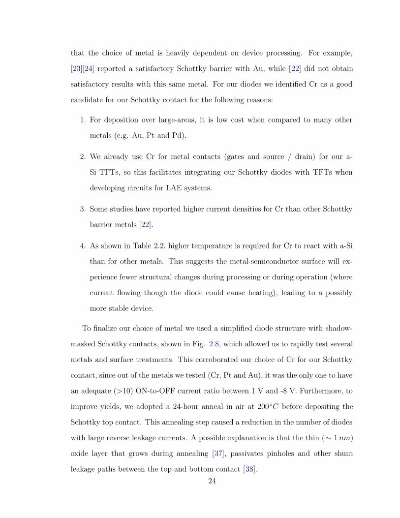
To finalize our choice of metal we used a simplified diode structure with shadow-
masked Schottky contacts, shown in Fig. 2.8, which allowed us to rapidly test several
metals and surface treatments. This corroborated our choice of Cr for our Schottky
contact, since out of the metals we tested (Cr, Pt and Au), it was the only one to have
an adequate (>10) ON-to-OFF current ratio between 1 V and -8 V. Furthermore, to
improve yields, we adopted a 24-hour anneal in air at 200◦C before depositing the
Schottky top contact. This annealing step caused a reduction in the number of diodes
with large reverse leakage currents. A possible explanation is that the thin (∼ 1 nm)
oxide layer that grows during annealing [37], passivates pinholes and other shunt
leakage paths between the top and bottom contact [38].
24
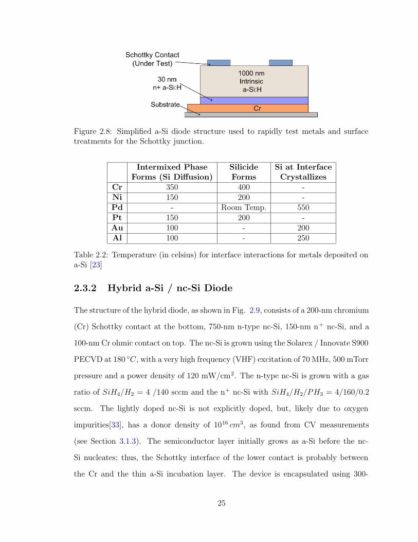
Figure 2.8: Simplified a-Si diode structure used to rapidly test metals and surfacetreatments for the Schottky junction.
Intermixed PhaseForms (Si Diffusion)
SilicideForms
Si at InterfaceCrystallizes
Cr 350 400 -Ni 150 200 -Pd - Room Temp. 550Pt 150 200 -Au 100 - 200Al 100 - 250
Table 2.2: Temperature (in celsius) for interface interactions for metals deposited ona-Si [23]
2.3.2 Hybrid a-Si / nc-Si Diode
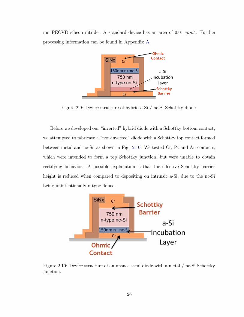
The structure of the hybrid diode, as shown in Fig. 2.9, consists of a 200-nm chromium
(Cr) Schottky contact at the bottom, 750-nm n-type nc-Si, 150-nm n+ nc-Si, and a
100-nm Cr ohmic contact on top. The nc-Si is grown using the Solarex / Innovate S900
PECVD at 180 ◦C, with a very high frequency (VHF) excitation of 70 MHz, 500 mTorr
pressure and a power density of 120 mW/cm2. The n-type nc-Si is grown with a gas
ratio of SiH4/H2 = 4 /140 sccm and the n+ nc-Si with SiH4/H2/PH3 = 4/160/0.2
sccm. The lightly doped nc-Si is not explicitly doped, but, likely due to oxygen
impurities[33], has a donor density of 1016 cm3, as found from CV measurements
(see Section 3.1.3). The semiconductor layer initially grows as a-Si before the nc-
Si nucleates; thus, the Schottky interface of the lower contact is probably between
the Cr and the thin a-Si incubation layer. The device is encapsulated using 300-
25
nm PECVD silicon nitride. A standard device has an area of 0.01 mm2. Further
processing information can be found in Appendix A.
Figure 2.9: Device structure of hybrid a-Si / nc-Si Schottky diode.
Before we developed our “inverted” hybrid diode with a Schottky bottom contact,
we attempted to fabricate a “non-inverted” diode with a Schottky top contact formed
between metal and nc-Si, as shown in Fig. 2.10. We tested Cr, Pt and Au contacts,
which were intended to form a top Schottky junction, but were unable to obtain
rectifying behavior. A possible explanation is that the effective Schottky barrier
height is reduced when compared to depositing on intrinsic a-Si, due to the nc-Si
being unintentionally n-type doped.
Figure 2.10: Device structure of an unsuccessful diode with a metal / nc-Si Schottkyjunction.
26
2.4 DC Characteristics
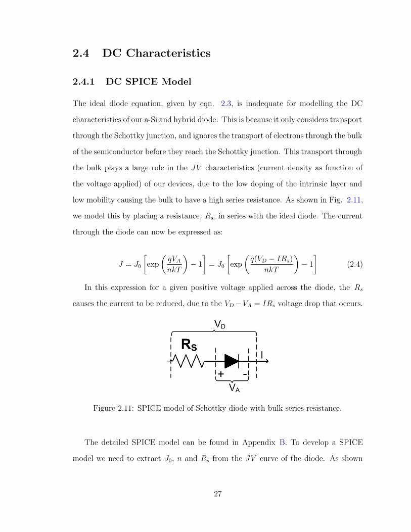
2.4.1 DC SPICE Model
The ideal diode equation, given by eqn. 2.3, is inadequate for modelling the DC
characteristics of our a-Si and hybrid diode. This is because it only considers transport
through the Schottky junction, and ignores the transport of electrons through the bulk
of the semiconductor before they reach the Schottky junction. This transport through
the bulk plays a large role in the JV characteristics (current density as function of
the voltage applied) of our devices, due to the low doping of the intrinsic layer and
low mobility causing the bulk to have a high series resistance. As shown in Fig. 2.11,
we model this by placing a resistance, Rs, in series with the ideal diode. The current
through the diode can now be expressed as:
J = J0
[
exp
(qVA
nkT
)
− 1
]
= J0
[
exp
(q(VD − IRs)
nkT
)
− 1
]
(2.4)
In this expression for a given positive voltage applied across the diode, the Rs
causes the current to be reduced, due to the VD −VA = IRs voltage drop that occurs.
Figure 2.11: SPICE model of Schottky diode with bulk series resistance.
The detailed SPICE model can be found in Appendix B. To develop a SPICE
model we need to extract J0, n and Rs from the JV curve of the diode. As shown
27
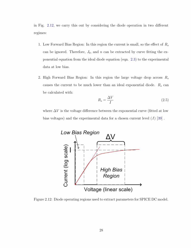
in Fig. 2.12, we carry this out by considering the diode operation in two different
regimes:
1. Low Forward Bias Region: In this region the current is small, so the effect of Rs
can be ignored. Therefore, J0, and n can be extracted by curve fitting the ex-
ponential equation from the ideal diode equation (eqn. 2.3) to the experimental
data at low bias.
2. High Forward Bias Region: In this region the large voltage drop across Rs
causes the current to be much lower than an ideal exponential diode. Rs can
be calculated with:
Rs =ΔV
I(2.5)
where ΔV is the voltage difference between the exponential curve (fitted at low
bias voltages) and the experimental data for a chosen current level (I) [39] .
Figure 2.12: Diode operating regions used to extract parameters for SPICE DC model.
28
2.4.2 a-Si Schottky Diode
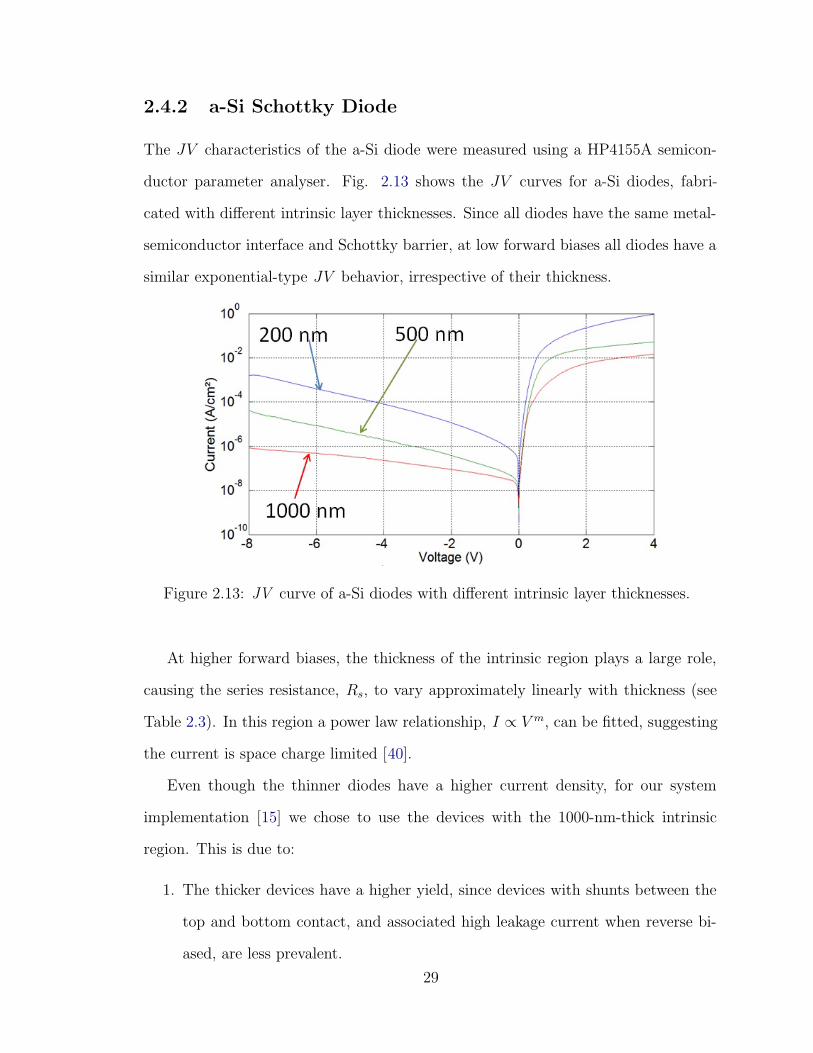
The JV characteristics of the a-Si diode were measured using a HP4155A semicon-
ductor parameter analyser. Fig. 2.13 shows the JV curves for a-Si diodes, fabri-
cated with different intrinsic layer thicknesses. Since all diodes have the same metal-
semiconductor interface and Schottky barrier, at low forward biases all diodes have a
similar exponential-type JV behavior, irrespective of their thickness.
Figure 2.13: JV curve of a-Si diodes with different intrinsic layer thicknesses.
At higher forward biases, the thickness of the intrinsic region plays a large role,
causing the series resistance, Rs, to vary approximately linearly with thickness (see
Table 2.3). In this region a power law relationship, I ∝ V m, can be fitted, suggesting
the current is space charge limited [40].
Even though the thinner diodes have a higher current density, for our system
implementation [15] we chose to use the devices with the 1000-nm-thick intrinsic
region. This is due to:
1. The thicker devices have a higher yield, since devices with shunts between the
top and bottom contact, and associated high leakage current when reverse bi-
ased, are less prevalent.
29
Intrin-sic
LayerThick-ness(nm)
Area(mm2)
Jo(A/cm2)
nRs
at 2V(Ω)
J at 1V(A/cm2)
J at -8V(A/cm2)
ON-to-OFF
CurrentRatio(from1V
to -8V)
a-Si250 1
5×10⁻⁸ 1.394600 4.9×10⁻² 1.6×10⁻³ 30
500 1 10000 1.0×10⁻² 4.0×10⁻⁵ 2501000 1 24000 1.1×10⁻³ 8.4×10⁻⁷ 1300
nc-Si 750 0.01 5×10⁻⁶ 1.31 200 6.6 1.1×10⁻³ 5500
Table 2.3: Comparison of parameters for a-Si and hybrid a-Si/nc-Si diode.
2. In most of our applications, there is sufficient area available on the substrate
to be able increase the size of the diode, so as to achieve the desired voltage
drop, while still having low leakage currents due to the thicker diodes larger
ON-to-OFF current ratio.
3. As explained in Section 3.1.2, for systems where the frequency performance
of the diode is important, all a-Si diodes, irrespective of their thickness, have
approximately the same cutoff frequency.
2.4.3 Hybrid a-Si / nc-Si Schottky Diode
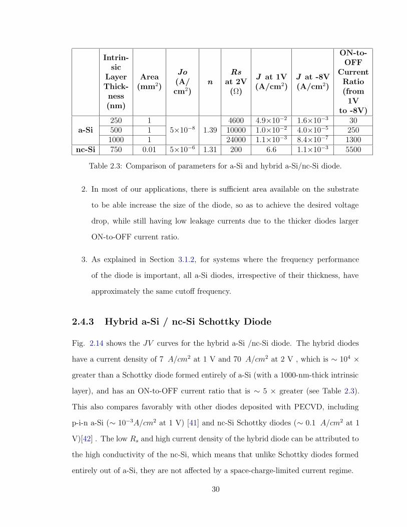
Fig. 2.14 shows the JV curves for the hybrid a-Si /nc-Si diode. The hybrid diodes
have a current density of 7 A/cm2 at 1 V and 70 A/cm2 at 2 V , which is ∼ 104 ×
greater than a Schottky diode formed entirely of a-Si (with a 1000-nm-thick intrinsic
layer), and has an ON-to-OFF current ratio that is ∼ 5 × greater (see Table 2.3).
This also compares favorably with other diodes deposited with PECVD, including
p-i-n a-Si (∼ 10−3A/cm2 at 1 V) [41] and nc-Si Schottky diodes (∼ 0.1 A/cm2 at 1
V)[42] . The low Rs and high current density of the hybrid diode can be attributed to
the high conductivity of the nc-Si, which means that unlike Schottky diodes formed
entirely out of a-Si, they are not affected by a space-charge-limited current regime.
30
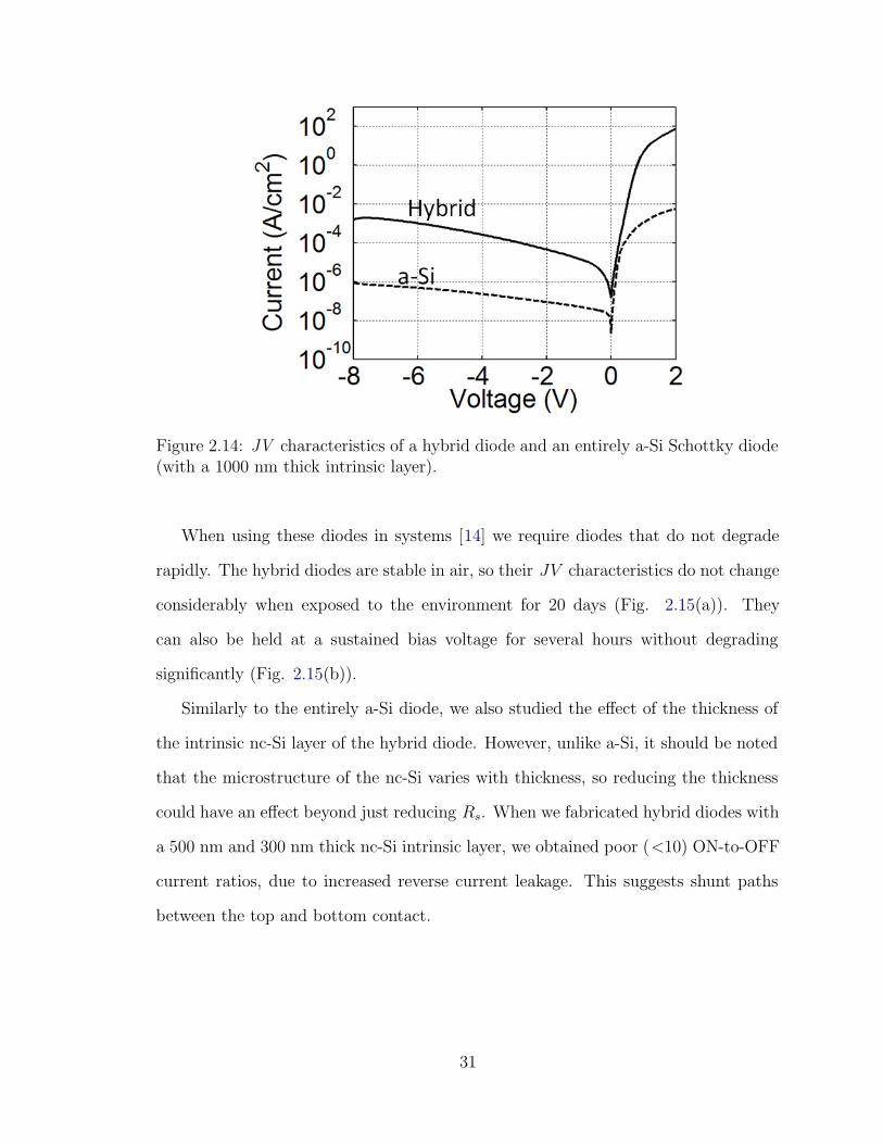
Figure 2.14: JV characteristics of a hybrid diode and an entirely a-Si Schottky diode(with a 1000 nm thick intrinsic layer).
When using these diodes in systems [14] we require diodes that do not degrade
rapidly. The hybrid diodes are stable in air, so their JV characteristics do not change
considerably when exposed to the environment for 20 days (Fig. 2.15(a)). They
can also be held at a sustained bias voltage for several hours without degrading
significantly (Fig. 2.15(b)).
Similarly to the entirely a-Si diode, we also studied the effect of the thickness of
the intrinsic nc-Si layer of the hybrid diode. However, unlike a-Si, it should be noted
that the microstructure of the nc-Si varies with thickness, so reducing the thickness
could have an effect beyond just reducing Rs. When we fabricated hybrid diodes with
a 500 nm and 300 nm thick nc-Si intrinsic layer, we obtained poor (<10) ON-to-OFF
current ratios, due to increased reverse current leakage. This suggests shunt paths
between the top and bottom contact.
31
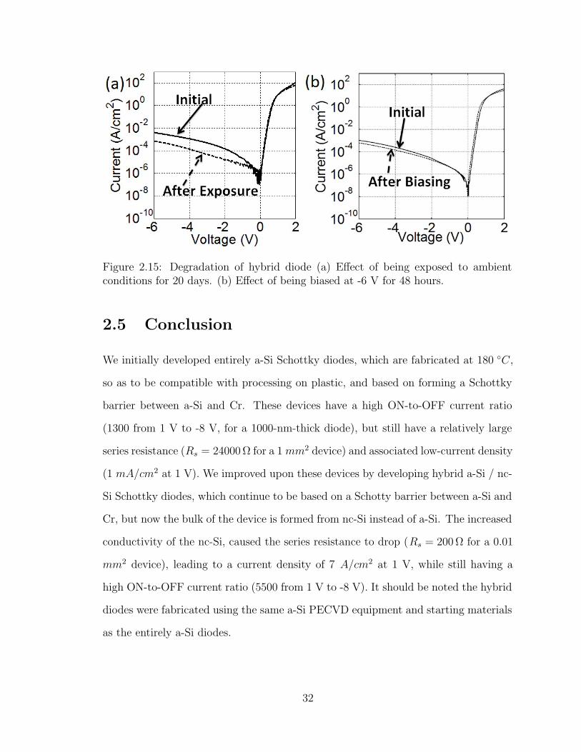
Figure 2.15: Degradation of hybrid diode (a) Effect of being exposed to ambientconditions for 20 days. (b) Effect of being biased at -6 V for 48 hours.
2.5 Conclusion
We initially developed entirely a-Si Schottky diodes, which are fabricated at 180 ◦C,
so as to be compatible with processing on plastic, and based on forming a Schottky
barrier between a-Si and Cr. These devices have a high ON-to-OFF current ratio
(1300 from 1 V to -8 V, for a 1000-nm-thick diode), but still have a relatively large
series resistance (Rs = 24000 Ω for a 1 mm2 device) and associated low-current density
(1 mA/cm2 at 1 V). We improved upon these devices by developing hybrid a-Si / nc-
Si Schottky diodes, which continue to be based on a Schotty barrier between a-Si and
Cr, but now the bulk of the device is formed from nc-Si instead of a-Si. The increased
conductivity of the nc-Si, caused the series resistance to drop (Rs = 200 Ω for a 0.01
mm2 device), leading to a current density of 7 A/cm2 at 1 V, while still having a
high ON-to-OFF current ratio (5500 from 1 V to -8 V). It should be noted the hybrid
diodes were fabricated using the same a-Si PECVD equipment and starting materials
as the entirely a-Si diodes.
32
Chapter 3
Diode AC Characteristics and
Thin-film Rectifiers
In Chapter 2 we studied the DC characteristics of an entirely a-Si and a hybrid a-
Si / nc-Si diode. However, for many LAE applications the AC characteristics are
equally important. One of the principal motivating applications for thin-film diodes
are RFID tags, which have been based on both organic [12] and metal-oxide rectifiers
[13]. The tag relies on a rectifier to convert a high frequency signal, received through
an inductive antenna, to DC. Another application we have been focusing on is large-
area sensing systems, based on laminating multiple sheets of thin-film electronics and
CMOS ICs. Non-contact inductive links are used to electrically connect the different
sheets and CMOS ICs, so once an AC signal is sent from sheet to another it needs to
be converted to DC. High frequencies are used, since this makes inductive links more
efficient [14]. These applications highlight the need for thin-film diodes for AC-to-DC
rectification at high frequencies.
In Section 3.1 we develop an AC SPICE model for both the a-Si and the hybrid
diode, based on experimental CV measurements. In Section 3.2 we test the high-
frequency performance of both our diodes by fabricating a half-wave rectifier for
33
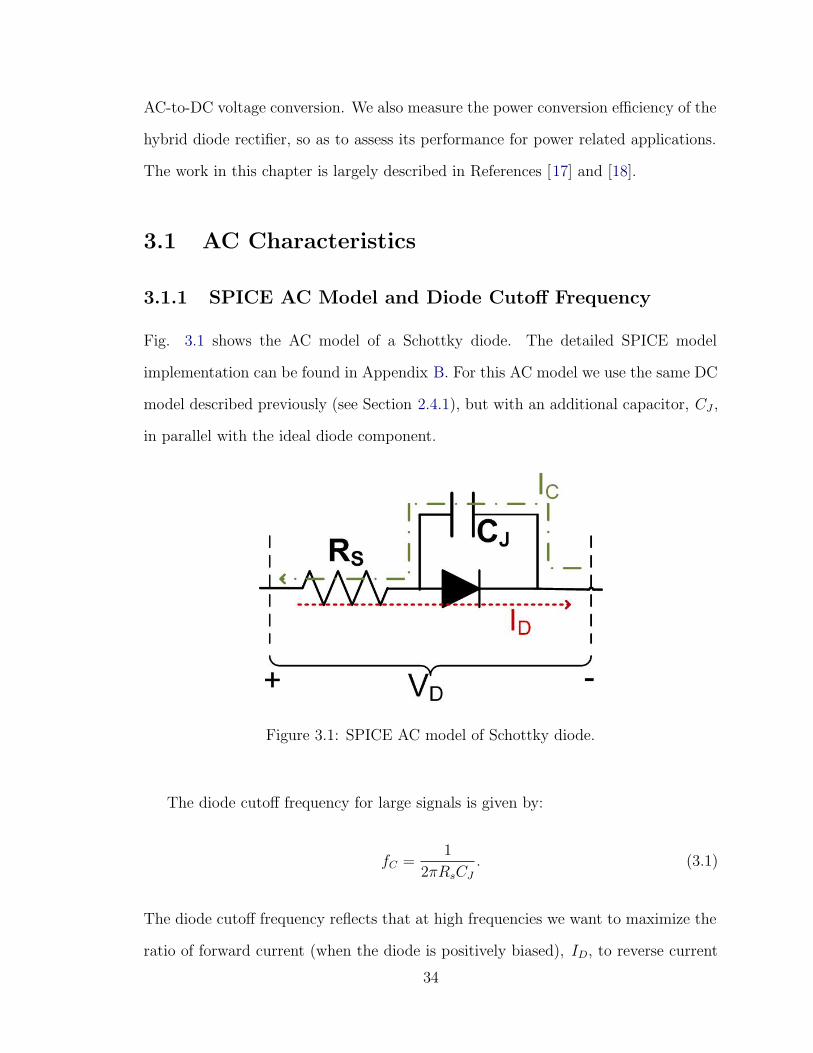
AC-to-DC voltage conversion. We also measure the power conversion efficiency of the
hybrid diode rectifier, so as to assess its performance for power related applications.
The work in this chapter is largely described in References [17] and [18].
3.1 AC Characteristics
3.1.1 SPICE AC Model and Diode Cutoff Frequency
Fig. 3.1 shows the AC model of a Schottky diode. The detailed SPICE model
implementation can be found in Appendix B. For this AC model we use the same DC
model described previously (see Section 2.4.1), but with an additional capacitor, CJ ,
in parallel with the ideal diode component.
Figure 3.1: SPICE AC model of Schottky diode.
The diode cutoff frequency for large signals is given by:
fC =1
2πRsCJ
. (3.1)
The diode cutoff frequency reflects that at high frequencies we want to maximize the
ratio of forward current (when the diode is positively biased), ID, to reverse current
34
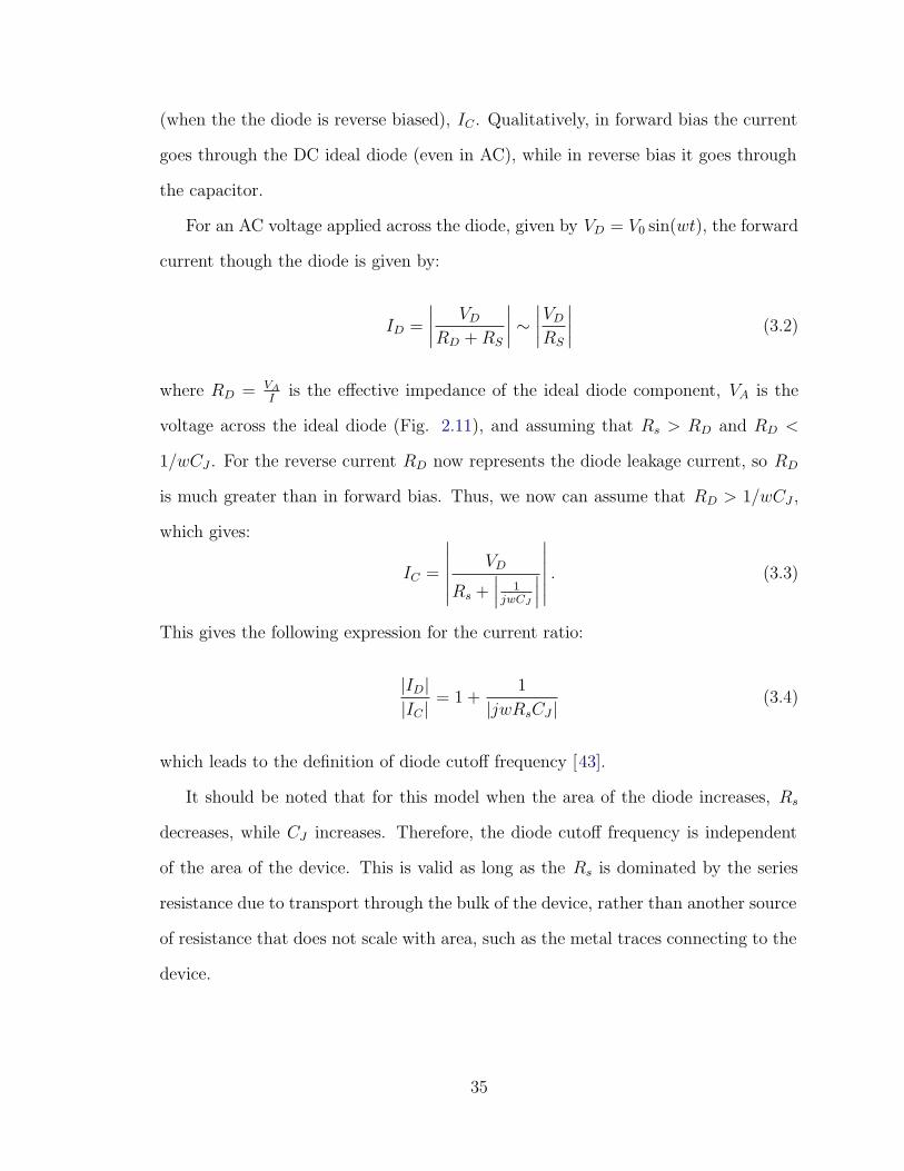
(when the the diode is reverse biased), IC . Qualitatively, in forward bias the current
goes through the DC ideal diode (even in AC), while in reverse bias it goes through
the capacitor.
For an AC voltage applied across the diode, given by VD = V0 sin(wt), the forward
current though the diode is given by:
ID =
∣∣∣∣
VD
RD + RS
∣∣∣∣ ∼
∣∣∣∣VD
RS
∣∣∣∣ (3.2)
where RD = VA
Iis the effective impedance of the ideal diode component, VA is the
voltage across the ideal diode (Fig. 2.11), and assuming that Rs > RD and RD <
1/wCJ . For the reverse current RD now represents the diode leakage current, so RD
is much greater than in forward bias. Thus, we now can assume that RD > 1/wCJ ,
which gives:
IC =
∣∣∣∣∣∣
VD
Rs +∣∣∣ 1jwCJ
∣∣∣
∣∣∣∣∣∣. (3.3)
This gives the following expression for the current ratio:
|ID||IC |
= 1 +1
|jwRsCJ |(3.4)
which leads to the definition of diode cutoff frequency [43].
It should be noted that for this model when the area of the diode increases, Rs
decreases, while CJ increases. Therefore, the diode cutoff frequency is independent
of the area of the device. This is valid as long as the Rs is dominated by the series
resistance due to transport through the bulk of the device, rather than another source
of resistance that does not scale with area, such as the metal traces connecting to the
device.
35
3.1.2 a-Si Schottky Diode
CV (capacitance as a function of voltage) measurements were carried out using a
HP 4280A capacitance meter at 1 MHz. Fig. 3.2 shows the CV measurements of
a-Si diodes with different intrinsic layer thicknesses. The capacitance measured re-
mains constant, irrespective of the reverse bias voltage that is applied. This indicates
that, due to the low doping density of the intrinsic a-Si, the depletion region extends
throughout the entirety of the intrinsic layer, starting at the Schottky contact and ter-
minating at the n+ doped a-Si layer. Therefore, the capacitance can be approximated
as:
CJ =ε
t(3.5)
where ε is the dielectric constant of a-Si and t is the thickness of the intrinsic layer
[23].
Figure 3.2: CV curve of a-Si diodes with different intrinsic layer thicknesses, measuredat 1 MHz.
Table 3.1 shows the cutoff frequencies for diodes with different thicknesses, calcu-
lated using Eqn. 3.1. Both Rs and CJ depend approximately linearly on the thickness
of the intrinsic layer, so thicker diodes have a larger Rs, but a smaller CJ . There-
36
fore, the cutoff frequency is not affected by the thickness of the intrinsic region. For
reasons explained in Section 2.4.2, we chose a thickness of 1000 nm for our standard
a-Si diode used for system development.
3.1.3 Hybrid a-Si / nc-Si Schottky Diode
Fig. 3.3 shows the CV curve of the hybrid a-Si / nc-Si Schottky diode. Although the
bulk nc-Si layer is not intentionally doped, due to impurities during deposition, it is
n-type (see Section 2.3.2). This means that unlike the entirely a-Si diode, the width
of the depletion region and associated capacitance varies depending on the reverse
bias voltage applied. Assuming the doping density, ND, of the nc-Si layer is constant,
the width of the depletion region can be expressed as:
wd =
√2εs
qND
(Vbi − VD) (3.6)
where Vbi is the built in voltage and VD is the voltage applied. Therefore, the capac-
itance is equal to:
CJ =εs
wd
=
√qεsND
2(Vbi − VD). (3.7)
This allows us to estimate the doping density of the nc-Si layer using:
ND =2
qεs
(−1
d(1/C2J)/dVD
)
(3.8)
[36, pp. 147-148] As shown in Fig. 3.4, this expression satisfactorily fits the ex-
perimental data, leading to an estimated doping density of the nc-Si bulk layer of
1016 cm−3.
As shown in Table 3.1, using a CJ of 7 pF (measured at 0 V), the hybrid diode has
a cutoff frequency of 110 MHz. This is ∼ 1000× greater than that of the entirely a-Si
diode, making it a good candidate for developing high frequency thin-film rectifiers.
37
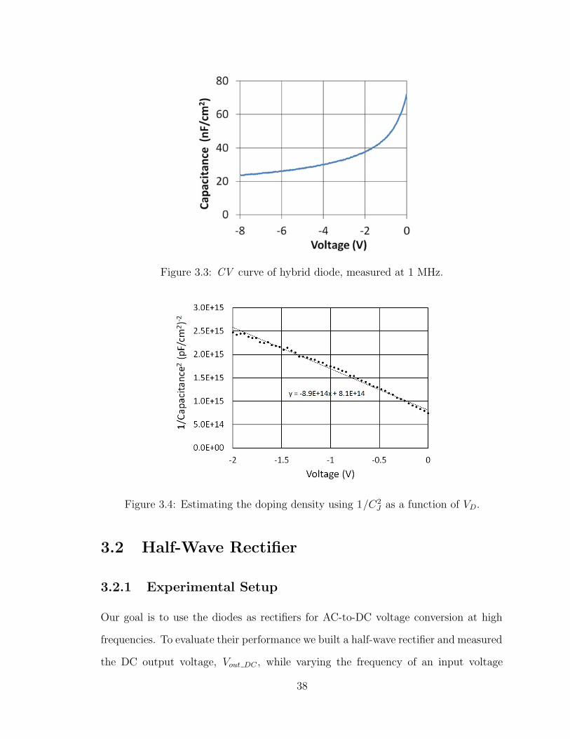
Figure 3.3: CV curve of hybrid diode, measured at 1 MHz.
Figure 3.4: Estimating the doping density using 1/C2J as a function of VD.
3.2 Half-Wave Rectifier
3.2.1 Experimental Setup
Our goal is to use the diodes as rectifiers for AC-to-DC voltage conversion at high
frequencies. To evaluate their performance we built a half-wave rectifier and measured
the DC output voltage, Vout DC , while varying the frequency of an input voltage
38
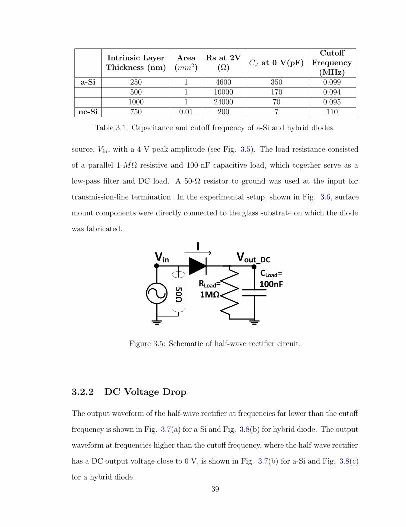
Intrinsic LayerThickness (nm)
Area(mm2)
Rs at 2V(Ω)
CJ at 0 V(pF)Cutoff
Frequency(MHz)
a-Si 250 1 4600 350 0.099500 1 10000 170 0.0941000 1 24000 70 0.095
nc-Si 750 0.01 200 7 110
Table 3.1: Capacitance and cutoff frequency of a-Si and hybrid diodes.
source, Vin, with a 4 V peak amplitude (see Fig. 3.5). The load resistance consisted
of a parallel 1-MΩ resistive and 100-nF capacitive load, which together serve as a
low-pass filter and DC load. A 50-Ω resistor to ground was used at the input for
transmission-line termination. In the experimental setup, shown in Fig. 3.6, surface
mount components were directly connected to the glass substrate on which the diode
was fabricated.
Figure 3.5: Schematic of half-wave rectifier circuit.
3.2.2 DC Voltage Drop
The output waveform of the half-wave rectifier at frequencies far lower than the cutoff
frequency is shown in Fig. 3.7(a) for a-Si and Fig. 3.8(b) for hybrid diode. The output
waveform at frequencies higher than the cutoff frequency, where the half-wave rectifier
has a DC output voltage close to 0 V, is shown in Fig. 3.7(b) for a-Si and Fig. 3.8(c)
for a hybrid diode.
39
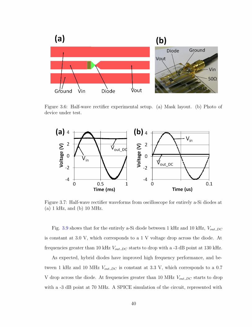
Figure 3.6: Half-wave rectifier experimental setup. (a) Mask layout. (b) Photo ofdevice under test.
Figure 3.7: Half-wave rectifier waveforms from oscilloscope for entirely a-Si diodes at(a) 1 kHz, and (b) 10 MHz.
Fig. 3.9 shows that for the entirely a-Si diode between 1 kHz and 10 kHz, Vout DC
is constant at 3.0 V, which corresponds to a 1 V voltage drop across the diode. At
frequencies greater than 10 kHz Vout DC starts to drop with a -3 dB point at 130 kHz.
As expected, hybrid diodes have improved high frequency performance, and be-
tween 1 kHz and 10 MHz Vout DC is constant at 3.3 V, which corresponds to a 0.7
V drop across the diode. At frequencies greater than 10 MHz Vout DC starts to drop
with a -3 dB point at 70 MHz. A SPICE simulation of the circuit, represented with
40
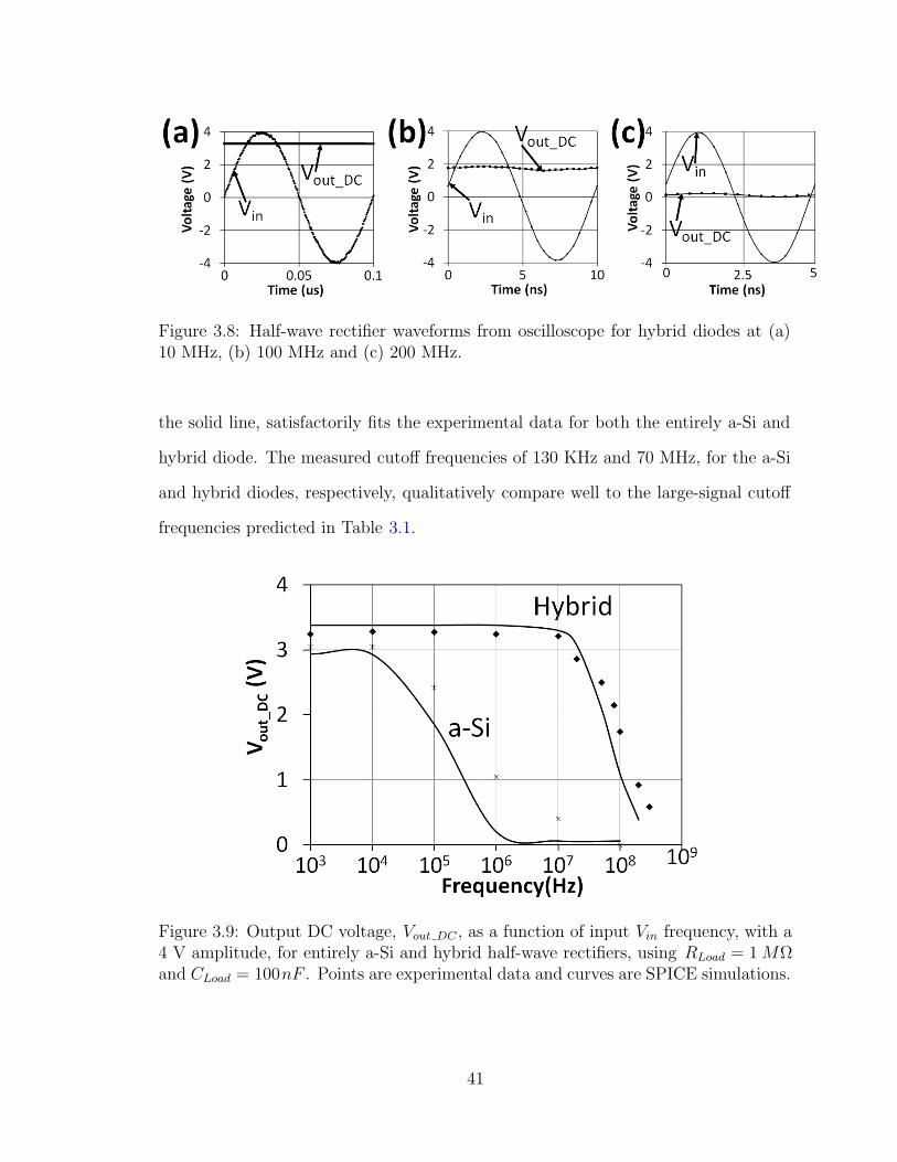
Figure 3.8: Half-wave rectifier waveforms from oscilloscope for hybrid diodes at (a)10 MHz, (b) 100 MHz and (c) 200 MHz.
the solid line, satisfactorily fits the experimental data for both the entirely a-Si and
hybrid diode. The measured cutoff frequencies of 130 KHz and 70 MHz, for the a-Si
and hybrid diodes, respectively, qualitatively compare well to the large-signal cutoff
frequencies predicted in Table 3.1.
Figure 3.9: Output DC voltage, Vout DC , as a function of input Vin frequency, with a4 V amplitude, for entirely a-Si and hybrid half-wave rectifiers, using RLoad = 1 MΩand CLoad = 100nF . Points are experimental data and curves are SPICE simulations.
41
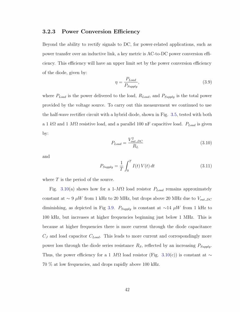
3.2.3 Power Conversion Efficiency
Beyond the ability to rectify signals to DC, for power-related applications, such as
power transfer over an inductive link, a key metric is AC-to-DC power conversion effi-
ciency. This efficiency will have an upper limit set by the power conversion efficiency
of the diode, given by:
η =PLoad
PSupply
, (3.9)
where PLoad is the power delivered to the load, RLoad, and PSupply is the total power
provided by the voltage source. To carry out this measurement we continued to use
the half-wave rectifier circuit with a hybrid diode, shown in Fig. 3.5, tested with both
a 1 kΩ and 1 MΩ resistive load, and a parallel 100 nF capacitive load. PLoad is given
by:
PLoad =V 2
out DC
RL
(3.10)
and
PSupply =1
T
∫ T
0
I(t) V (t) dt (3.11)
where T is the period of the source.
Fig. 3.10(a) shows how for a 1-MΩ load resistor PLoad remains approximately
constant at ∼ 9 μW from 1 kHz to 20 MHz, but drops above 20 MHz due to Vout DC
diminishing, as depicted in Fig 3.9. PSupply is constant at ∼14 μW from 1 kHz to
100 kHz, but increases at higher frequencies beginning just below 1 MHz. This is
because at higher frequencies there is more current through the diode capacitance
CJ and load capacitor CLoad. This leads to more current and correspondingly more
power loss through the diode series resistance RS, reflected by an increasing PSupply.
Thus, the power efficiency for a 1 MΩ load resistor (Fig. 3.10(c)) is constant at ∼
70 % at low frequencies, and drops rapidly above 100 kHz.
42
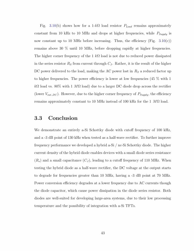
Fig. 3.10(b) shows how for a 1-kΩ load resistor PLoad remains approximately
constant from 10 kHz to 10 MHz and drops at higher frequencies, while PSupply is
now constant up to 10 MHz before increasing. Thus, the efficiency (Fig. 3.10(c))
remains above 30 % until 10 MHz, before dropping rapidly at higher frequencies.
The higher corner frequency of the 1 kΩ load is not due to reduced power dissipated
in the series resistor RS from current through CJ . Rather, it is the result of the higher
DC power delivered to the load, making the AC power lost in RS a reduced factor up
to higher frequencies. The power efficiency is lower at low frequencies (45 % with 1
kΩ load vs. 80% with 1 MΩ load) due to a larger DC diode drop across the rectifier
(lower Vout DC). However, due to the higher corner frequency of PSupply, the efficiency
remains approximately constant to 10 MHz instead of 100 kHz for the 1 MΩ load.
3.3 Conclusion
We demonstrate an entirely a-Si Schottky diode with cutoff frequency of 100 kHz,
and a -3 dB point of 130 kHz when tested as a half-wave rectifier. To further improve
frequency performance we developed a hybrid a-Si / nc-Si Schottky diode. The higher
current density of the hybrid diode enables devices with a small diode series resistance
(Rs) and a small capacitance (CJ), leading to a cutoff frequency of 110 MHz. When
testing the hybrid diode as a half-wave rectifier, the DC voltage at the output starts
to degrade for frequencies greater than 10 MHz, having a -3 dB point at 70 MHz.
Power conversion efficiency degrades at a lower frequency due to AC currents though
the diode capacitor, which cause power dissipation in the diode series resistor. Both
diodes are well-suited for developing large-area systems, due to their low processing
temperature and the possibility of integration with a-Si TFTs.
43

3.4 Acknowledgments
The thin-film diodes were integrated with non-contact inductive interfaces, as part of
a large-area structural health monitoring system, by Yingzhe Hu.
44
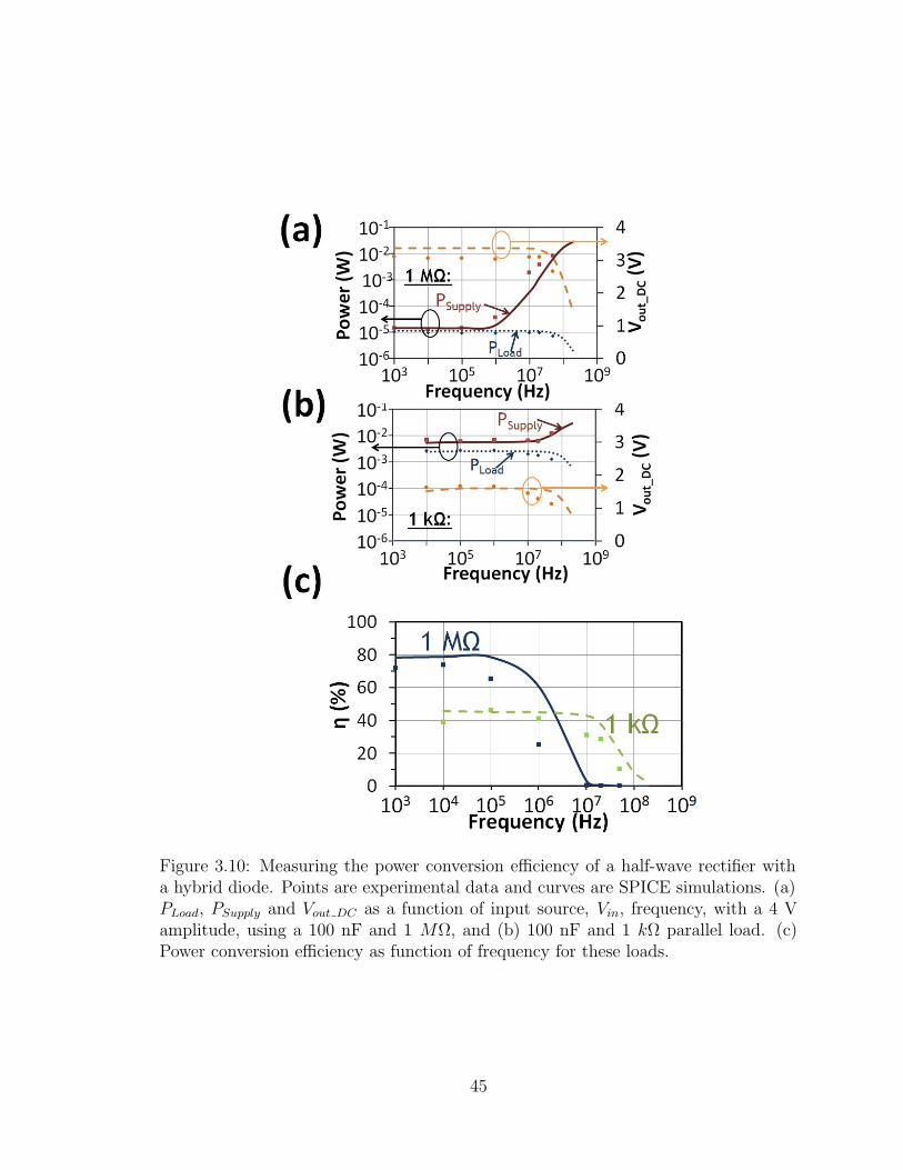
Figure 3.10: Measuring the power conversion efficiency of a half-wave rectifier witha hybrid diode. Points are experimental data and curves are SPICE simulations. (a)PLoad, PSupply and Vout DC as a function of input source, Vin, frequency, with a 4 Vamplitude, using a 100 nF and 1 MΩ, and (b) 100 nF and 1 kΩ parallel load. (c)Power conversion efficiency as function of frequency for these loads.
45
Chapter 4
System Development: Large-Area
Microphone Array for Source
Separation Based on a Hybrid
Architecture Exploiting Thin-film
Electronics and CMOS
As electronics becomes ever more pervasive in our daily lives, it will no longer be
confined to our phones and tablets, but rather will be seamlessly integrated into the
physical environment in which we live, work, and play. In such a form factor, there is
an opportunity for systems that foster collaborative spaces and enhance interpersonal
interactions. With this motivation, we present a system that enables voice signals
from multiple simultaneous speakers to be separated and reconstructed, ultimately to
be fed to a voice-command recognition engine for controlling electronic systems. The
cornerstone of the system is a spatially-distributed microphone array, which exploits
the diversity of the audio signal received by different microphones in order to separate
46
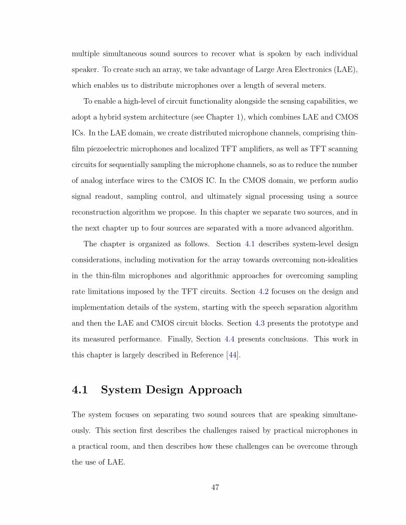
multiple simultaneous sound sources to recover what is spoken by each individual
speaker. To create such an array, we take advantage of Large Area Electronics (LAE),
which enables us to distribute microphones over a length of several meters.
To enable a high-level of circuit functionality alongside the sensing capabilities, we
adopt a hybrid system architecture (see Chapter 1), which combines LAE and CMOS
ICs. In the LAE domain, we create distributed microphone channels, comprising thin-
film piezoelectric microphones and localized TFT amplifiers, as well as TFT scanning
circuits for sequentially sampling the microphone channels, so as to reduce the number
of analog interface wires to the CMOS IC. In the CMOS domain, we perform audio
signal readout, sampling control, and ultimately signal processing using a source
reconstruction algorithm we propose. In this chapter we separate two sources, and in
the next chapter up to four sources are separated with a more advanced algorithm.
The chapter is organized as follows. Section 4.1 describes system-level design
considerations, including motivation for the array towards overcoming non-idealities
in the thin-film microphones and algorithmic approaches for overcoming sampling
rate limitations imposed by the TFT circuits. Section 4.2 focuses on the design and
implementation details of the system, starting with the speech separation algorithm
and then the LAE and CMOS circuit blocks. Section 4.3 presents the prototype and
its measured performance. Finally, Section 4.4 presents conclusions. This work in
this chapter is largely described in Reference [44].
4.1 System Design Approach
The system focuses on separating two sound sources that are speaking simultane-
ously. This section first describes the challenges raised by practical microphones in
a practical room, and then describes how these challenges can be overcome through
the use of LAE.
47
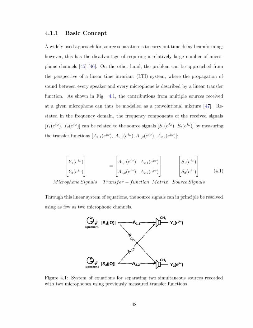
4.1.1 Basic Concept
A widely used approach for source separation is to carry out time delay beamforming;
however, this has the disadvantage of requiring a relatively large number of micro-
phone channels [45] [46]. On the other hand, the problem can be approached from
the perspective of a linear time invariant (LTI) system, where the propagation of
sound between every speaker and every microphone is described by a linear transfer
function. As shown in Fig. 4.1, the contributions from multiple sources received
at a given microphone can thus be modelled as a convolutional mixture [47]. Re-
stated in the frequency domain, the frequency components of the received signals
[Y1(ejω), Y2(e
jω)] can be related to the source signals [S1(ejω), S2(e
jω)] by measuring
the transfer functions [A1,1(ejω), A2,1(e
jω), A1,2(ejω), A2,2(e
jω)]:
Y1(ejω)
Y2(ejω)
=
A1,1(ejω) A2,1(e
jω)
A1,2(ejω) A2,2(e
jω)
S1(ejω)
S2(ejω)
Microphone Signals Transfer − function Matrix Source Signals
(4.1)
Through this linear system of equations, the source signals can in principle be resolved
using as few as two microphone channels.
CH1
CH2
|S1(j )| A1,1
A2,2
A 2,1
A1,2
|S2(j )|
Speaker 1
Speaker 2Y2(e
j )
Y1(ej )
Figure 4.1: System of equations for separating two simultaneous sources recordedwith two microphones using previously measured transfer functions.
48
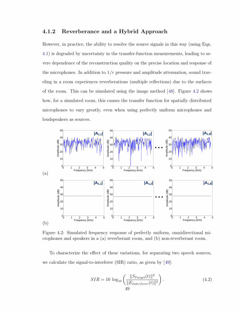
4.1.2 Reverberance and a Hybrid Approach
However, in practice, the ability to resolve the source signals in this way (using Eqn.
4.1) is degraded by uncertainty in the transfer-function measurements, leading to se-
vere dependence of the reconstruction quality on the precise location and response of
the microphones. In addition to 1/r pressure and amplitude attenuation, sound trav-
eling in a room experiences reverberations (multiple reflections) due to the surfaces
of the room. This can be simulated using the image method [48]. Figure 4.2 shows
how, for a simulated room, this causes the transfer function for spatially distributed
microphones to vary greatly, even when using perfectly uniform microphones and
loudspeakers as sources.
(a)
0 1 2 3 4 50
10
20
30
40
50
Frequency (kHz)
Am
plitu
de (
dB)
0 1 2 3 4 50
10
20
30
40
50
Frequency (kHz)
Am
plitu
de (
dB)
0 1 2 3 4 50
10
20
30
40
50
Frequency (kHz)A
mpl
itude
(dB
)
|A1,1| |A1,2| |A1,8|
...
(b)
0 1 2 3 4 50
10
20
30
40
50
Frequency (kHz)
Am
plitu
de (
dB)
0 1 2 3 4 50
10
20
30
40
50
Frequency (kHz)
Am
plitu
de (
dB)
0 1 2 3 4 50
10
20
30
40
50
Frequency (kHz)
Am
plitu
de (
dB)
...|A1,1| |A1,2| |A1,8|
Figure 4.2: Simulated frequency response of perfectly uniform, omnidirectional mi-crophones and speakers in a (a) reverberant room, and (b) non-reverberant room.
To characterize the effect of these variations, for separating two speech sources,
we calculate the signal-to-interferer (SIR) ratio, as given by [49]:
SIR = 10 log10
(‖STarget(t)‖2
‖EInterferer(t)‖2
)
. (4.2)
49
STarget(t) is the original sound source we wish to recover, while EInterferer(t) is the
remaining component from the second source, which has not been fully removed by
the separation algorithm. Fig. 4.3(a) shows a simulation in an ideal anechoic room,
wherein room reverberations, microphone variations, and microphone directionality
are not considered. The room parameters used for simulations throughout this chap-
ter are shown in Fig. 4.4. In this simulation, 8 microphones are incorporated in a
linear array with spacing of 15 cm (array width = 105 cm), but only two are selected
for source separation using the approach in Equation 4.1. Each of the 8-choose-2
microphone permutations (56 possible pairs) are examined. A 10 s speech segment is
used as the sound emitted by each simulated source. Each segment consists of three
sentences from Male A and Female B speaker from the TSP Speech Database [50].
Each is processed by concatenating 100 ms windows, as outlined in Section 4.2.5.2.
The results show that nearly uniform SIR improvement (24 dB, relative to the unpro-
cessed input signal) is achieved regardless of the two microphones selected. “Noise”
is not yet considered. On the other hand, Fig. 4.3(b) shows a simulation considering
practical levels of room reverberations, microphone variations, and microphone direc-
tionality. In this case, the SIR improvement varies greatly (from 6 dB to 20 dB)
due to the intrinsic and positional variations of the microphones. Furthermore, for
the thin-film microphones made in our lab, variations in frequency and directionality
response (Section 4.2.1) can affect the performance of a system based on only a small
number of microphones.
To mitigate this variation, we propose an approach that takes advantage of LAE
in two ways:
1. By having multiple spatially-distributed microphones, we can select a sub-array
that is closest to the two speakers, as illustrated in Fig. 4.5. This allows us to
receive the highest SNR signal, enabling higher quality microphone recordings
and improved transfer function estimates.
50
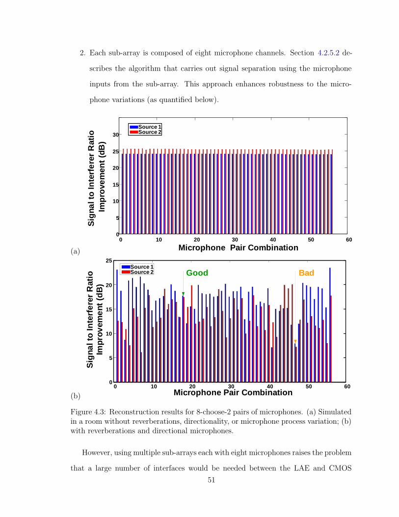
2. Each sub-array is composed of eight microphone channels. Section 4.2.5.2 de-
scribes the algorithm that carries out signal separation using the microphone
inputs from the sub-array. This approach enhances robustness to the micro-
phone variations (as quantified below).
(a)
0 10 20 30 40 50 600
5
10
15
20
25
30
Microphone Pair Combination
Sig
nal t
o In
terf
erer
Rat
ioIm
prov
emen
t (dB
)
Source 1
Source 2
(b)
Source 1Source 2
0 10 20 30 40 50 600
5
10
15
20
25
Microphone Pair Combination
Sig
nal t
o In
terfe
rer
Rat
io
Impr
ovem
ent (
dB)
Good Bad
Figure 4.3: Reconstruction results for 8-choose-2 pairs of microphones. (a) Simulatedin a room without reverberations, directionality, or microphone process variation; (b)with reverberations and directional microphones.
However, using multiple sub-arrays each with eight microphones raises the problem
that a large number of interfaces would be needed between the LAE and CMOS
51
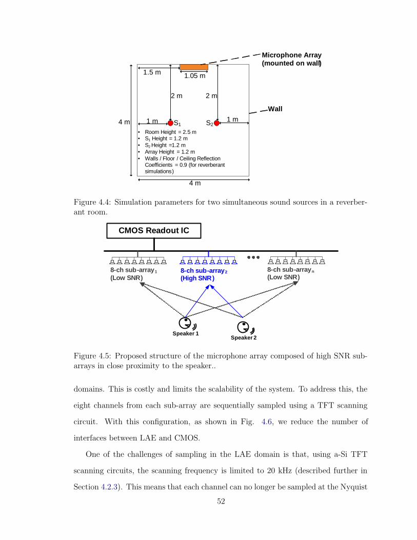
4 m
4 m
1 m1 m
2 m 2 m
S1 S2
• Room Height = 2.5 m• S1 Height = 1.2 m• S2 Height =1.2 m• Array Height = 1.2 m• Walls / Floor / Ceiling Reflection
Coefficients = 0.9 (for reverberant simulations)
1.05 m1.5 m
Wall
Microphone Array (mounted on wall)
Figure 4.4: Simulation parameters for two simultaneous sound sources in a reverber-ant room.
Speaker 2
CMOS Readout IC
8-ch sub-array 1
(Low SNR)8-ch sub-array n
(Low SNR)8-ch sub-array 2
(High SNR)
Speaker 1
Figure 4.5: Proposed structure of the microphone array composed of high SNR sub-arrays in close proximity to the speaker..
domains. This is costly and limits the scalability of the system. To address this, the
eight channels from each sub-array are sequentially sampled using a TFT scanning
circuit. With this configuration, as shown in Fig. 4.6, we reduce the number of
interfaces between LAE and CMOS.
One of the challenges of sampling in the LAE domain is that, using a-Si TFT
scanning circuits, the scanning frequency is limited to 20 kHz (described further in
Section 4.2.3). This means that each channel can no longer be sampled at the Nyquist
52
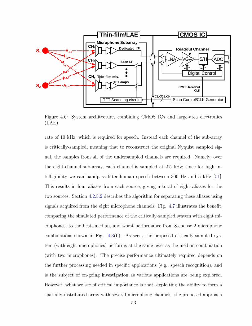
S1
S2
A1,1
A1,2
A1,8
A2,8
A 2,1
TFT Scanning circuit
CH1
CH2
CH8A 2,2
LNA S/H ADC
Thin-film/LAE
VGA
Thin-film mic.
TFT amps
Dedicated I/F
Scan I /F
Microphone Subarray
Readout Channel
Scan Control/CLK Generator
CMOS IC
Digital Control
CLK/CLKb
CMOS Readout CLK
Figure 4.6: System architecture, combining CMOS ICs and large-area electronics(LAE).
rate of 10 kHz, which is required for speech. Instead each channel of the sub-array
is critically-sampled, meaning that to reconstruct the original Nyquist sampled sig-
nal, the samples from all of the undersampled channels are required. Namely, over
the eight-channel sub-array, each channel is sampled at 2.5 kHz; since for high in-
telligibility we can bandpass filter human speech between 300 Hz and 5 kHz [51].
This results in four aliases from each source, giving a total of eight aliases for the
two sources. Section 4.2.5.2 describes the algorithm for separating these aliases using
signals acquired from the eight microphone channels. Fig. 4.7 illustrates the benefit,
comparing the simulated performance of the critically-sampled system with eight mi-
crophones, to the best, median, and worst performance from 8-choose-2 microphone
combinations shown in Fig. 4.3(b). As seen, the proposed critically-sampled sys-
tem (with eight microphones) performs at the same level as the median combination
(with two microphones). The precise performance ultimately required depends on
the further processing needed in specific applications (e.g., speech recognition), and
is the subject of on-going investigation as various applications are being explored.
However, what we see of critical importance is that, exploiting the ability to form a
spatially-distributed array with several microphone channels, the proposed approach
53
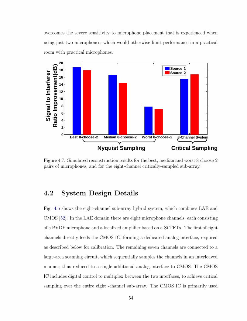
overcomes the severe sensitivity to microphone placement that is experienced when
using just two microphones, which would otherwise limit performance in a practical
room with practical microphones.
Best 8-choose-2 Median 8-choose-2 Worst 8-choose-2 8-Channel System0
2
4
6
8
10
12
14
16
18
20
Sig
nal t
o In
terf
erer
R
atio
Impr
ovem
ent(
dB) Source 1
Source 2
Nyquist Sampling Critical Sampling
Figure 4.7: Simulated reconstruction results for the best, median and worst 8-choose-2pairs of microphones, and for the eight-channel critically-sampled sub-array.
4.2 System Design Details
Fig. 4.6 shows the eight-channel sub-array hybrid system, which combines LAE and
CMOS [52]. In the LAE domain there are eight microphone channels, each consisting
of a PVDF microphone and a localized amplifier based on a-Si TFTs. The first of eight
channels directly feeds the CMOS IC, forming a dedicated analog interface, required
as described below for calibration. The remaining seven channels are connected to a
large-area scanning circuit, which sequentially samples the channels in an interleaved
manner; thus reduced to a single additional analog interface to CMOS. The CMOS
IC includes digital control to multiplex between the two interfaces, to achieve critical
sampling over the entire eight -channel sub-array. The CMOS IC is primarily used
54
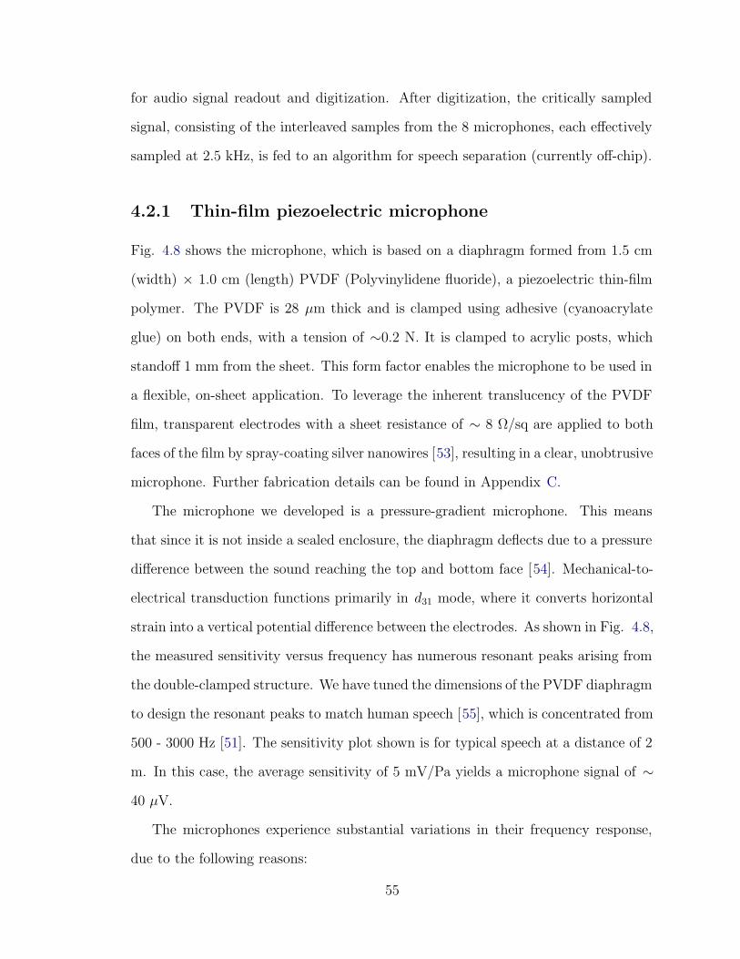
for audio signal readout and digitization. After digitization, the critically sampled
signal, consisting of the interleaved samples from the 8 microphones, each effectively
sampled at 2.5 kHz, is fed to an algorithm for speech separation (currently off-chip).
4.2.1 Thin-film piezoelectric microphone
Fig. 4.8 shows the microphone, which is based on a diaphragm formed from 1.5 cm
(width) × 1.0 cm (length) PVDF (Polyvinylidene fluoride), a piezoelectric thin-film
polymer. The PVDF is 28 μm thick and is clamped using adhesive (cyanoacrylate
glue) on both ends, with a tension of ∼0.2 N. It is clamped to acrylic posts, which
standoff 1 mm from the sheet. This form factor enables the microphone to be used in
a flexible, on-sheet application. To leverage the inherent translucency of the PVDF
film, transparent electrodes with a sheet resistance of ∼ 8 Ω/sq are applied to both
faces of the film by spray-coating silver nanowires [53], resulting in a clear, unobtrusive
microphone. Further fabrication details can be found in Appendix C.
The microphone we developed is a pressure-gradient microphone. This means
that since it is not inside a sealed enclosure, the diaphragm deflects due to a pressure
difference between the sound reaching the top and bottom face [54]. Mechanical-to-
electrical transduction functions primarily in d31 mode, where it converts horizontal
strain into a vertical potential difference between the electrodes. As shown in Fig. 4.8,
the measured sensitivity versus frequency has numerous resonant peaks arising from
the double-clamped structure. We have tuned the dimensions of the PVDF diaphragm
to design the resonant peaks to match human speech [55], which is concentrated from
500 - 3000 Hz [51]. The sensitivity plot shown is for typical speech at a distance of 2
m. In this case, the average sensitivity of 5 mV/Pa yields a microphone signal of ∼
40 μV.
The microphones experience substantial variations in their frequency response,
due to the following reasons:
55
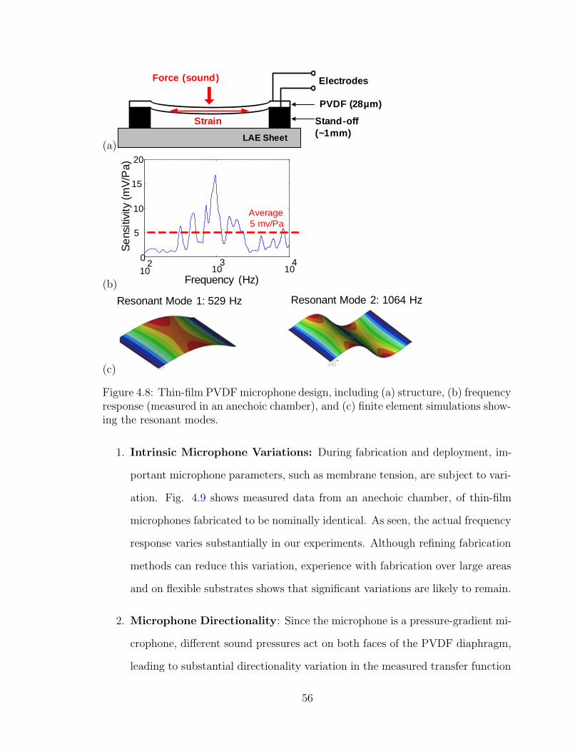
(a)
Stand-off (~1mm)
PVDF (28µm)
Force (sound)
Strain
LAE Sheet
Electrodes
(b)10
210
310
40
5
10
15
20
Frequency (Hz)
Se
nsiti
vity
(m
V/P
a)
Average5 mv/Pa
(c)
Resonant Mode 1: 529 Hz Resonant Mode 2: 1064 Hz
Figure 4.8: Thin-film PVDF microphone design, including (a) structure, (b) frequencyresponse (measured in an anechoic chamber), and (c) finite element simulations show-ing the resonant modes.
1. Intrinsic Microphone Variations: During fabrication and deployment, im-
portant microphone parameters, such as membrane tension, are subject to vari-
ation. Fig. 4.9 shows measured data from an anechoic chamber, of thin-film
microphones fabricated to be nominally identical. As seen, the actual frequency
response varies substantially in our experiments. Although refining fabrication
methods can reduce this variation, experience with fabrication over large areas
and on flexible substrates shows that significant variations are likely to remain.
2. Microphone Directionality: Since the microphone is a pressure-gradient mi-
crophone, different sound pressures act on both faces of the PVDF diaphragm,
leading to substantial directionality variation in the measured transfer function
56
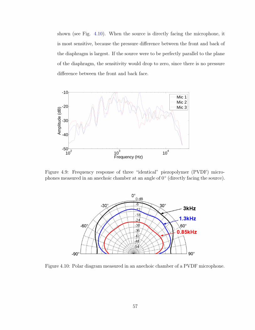
shown (see Fig. 4.10). When the source is directly facing the microphone, it
is most sensitive, because the pressure difference between the front and back of
the diaphragm is largest. If the source were to be perfectly parallel to the plane
of the diaphragm, the sensitivity would drop to zero, since there is no pressure
difference between the front and back face.
102
103
104-50
-40
-30
-20
-10
Frequency (Hz)
Am
plitu
de (
dB)
Mic 1Mic 2Mic 3
Figure 4.9: Frequency response of three “identical” piezopolymer (PVDF) micro-phones measured in an anechoic chamber at an angle of 0◦ (directly facing the source).
Figure 4.10: Polar diagram measured in an anechoic chamber of a PVDF microphone.
57
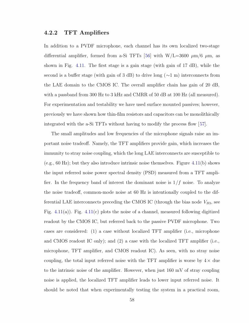
4.2.2 TFT Amplifiers
In addition to a PVDF microphone, each channel has its own localized two-stage
differential amplifier, formed from a-Si TFTs [56] with W/L=3600 μm/6 μm, as
shown in Fig. 4.11. The first stage is a gain stage (with gain of 17 dB), while the
second is a buffer stage (with gain of 3 dB) to drive long (∼1 m) interconnects from
the LAE domain to the CMOS IC. The overall amplifier chain has gain of 20 dB,
with a passband from 300 Hz to 3 kHz and CMRR of 50 dB at 100 Hz (all measured).
For experimentation and testability we have used surface mounted passives; however,
previously we have shown how thin-film resistors and capacitors can be monolithically
integrated with the a-Si TFTs without having to modify the process flow [57].
The small amplitudes and low frequencies of the microphone signals raise an im-
portant noise tradeoff. Namely, the TFT amplifiers provide gain, which increases the
immunity to stray noise coupling, which the long LAE interconnects are susceptible to
(e.g., 60 Hz); but they also introduce intrinsic noise themselves. Figure 4.11(b) shows
the input referred noise power spectral density (PSD) measured from a TFT ampli-
fier. In the frequency band of interest the dominant noise is 1/f noise. To analyze
the noise tradeoff, common-mode noise at 60 Hz is intentionally coupled to the dif-
ferential LAE interconnects preceding the CMOS IC (through the bias node VB3, see
Fig. 4.11(a)). Fig. 4.11(c) plots the noise of a channel, measured following digitized
readout by the CMOS IC, but referred back to the passive PVDF microphone. Two
cases are considered: (1) a case without localized TFT amplifier (i.e., microphone
and CMOS readout IC only); and (2) a case with the localized TFT amplifier (i.e.,
microphone, TFT amplifier, and CMOS readout IC). As seen, with no stray noise
coupling, the total input referred noise with the TFT amplifier is worse by 4× due
to the intrinsic noise of the amplifier. However, when just 160 mV of stray coupling
noise is applied, the localized TFT amplifier leads to lower input referred noise. It
should be noted that when experimentally testing the system in a practical room,
58
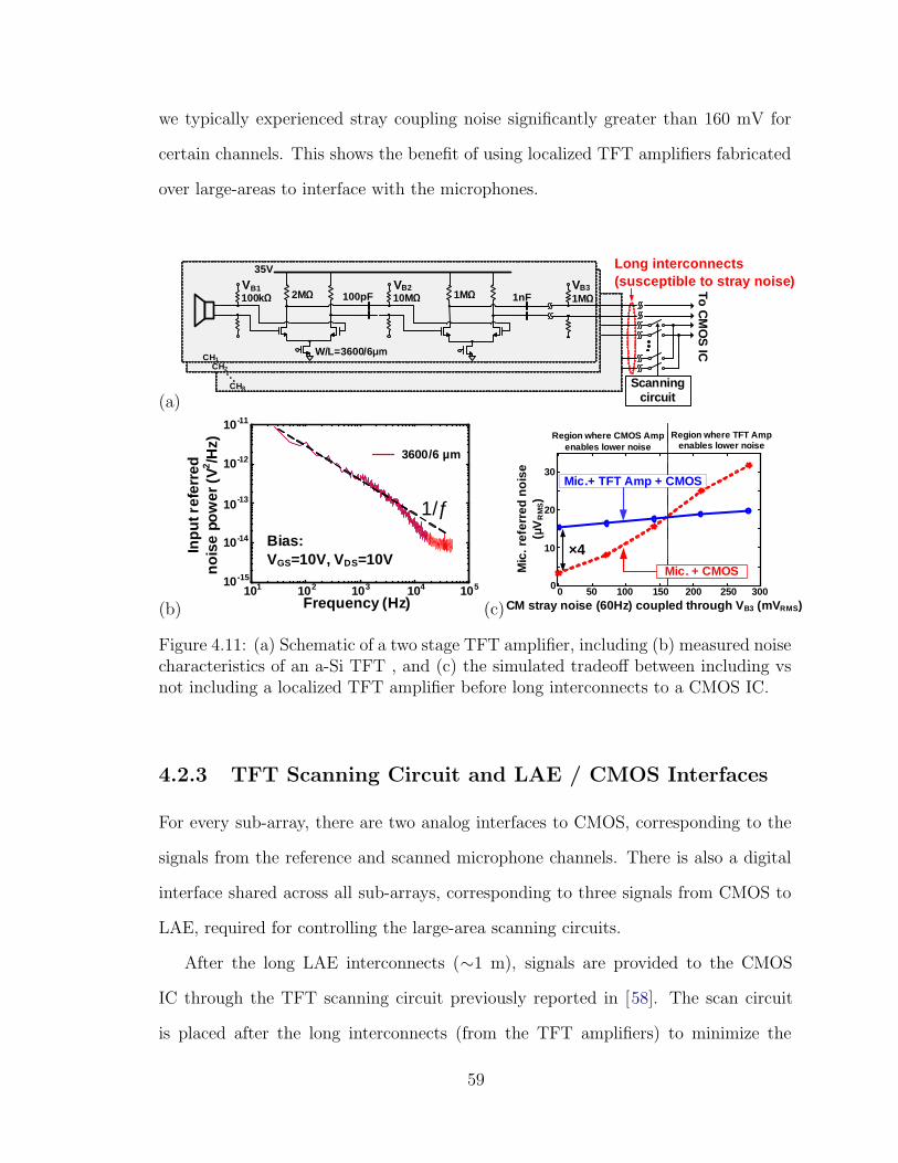
we typically experienced stray coupling noise significantly greater than 160 mV for
certain channels. This shows the benefit of using localized TFT amplifiers fabricated
over large-areas to interface with the microphones.
(a)Scanning
circuit
W/L=3600/6
2M 1M 1M10M100pF 1nF100kVB2 VB3
35V
VB1
Long interconnects(susceptible to stray noise)
CH1CH2
CH8
To CM
OS
IC
(b)101
10-11
10-12
10-13
10-14
10-15
102 103 104 105
Bias:VGS=10V, VDS=10V
Frequency (Hz)
Inpu
t ref
erre
d no
ise
pow
er (
V2/H
z)
3600/6 µm
1/ƒ
(c)
Mic
. ref
erre
d no
ise
(V
RM
S)
0 50 100 150 200 250 3000
10
20
30
CM stray noise (60Hz) coupled through V B3 (mVRMS)
Mic.+ TFT Amp + CMOS
×4Mic. + CMOS
Region where TFT Amp enables lower noise
Region where CMOS Amp enables lower noise
Figure 4.11: (a) Schematic of a two stage TFT amplifier, including (b) measured noisecharacteristics of an a-Si TFT , and (c) the simulated tradeoff between including vsnot including a localized TFT amplifier before long interconnects to a CMOS IC.
4.2.3 TFT Scanning Circuit and LAE / CMOS Interfaces
For every sub-array, there are two analog interfaces to CMOS, corresponding to the
signals from the reference and scanned microphone channels. There is also a digital
interface shared across all sub-arrays, corresponding to three signals from CMOS to
LAE, required for controlling the large-area scanning circuits.
After the long LAE interconnects (∼1 m), signals are provided to the CMOS
IC through the TFT scanning circuit previously reported in [58]. The scan circuit
is placed after the long interconnects (from the TFT amplifiers) to minimize the
59
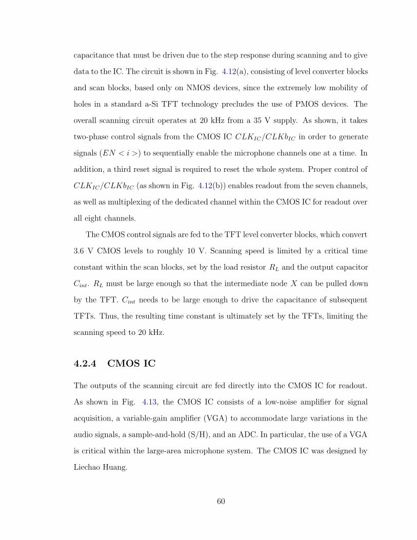
capacitance that must be driven due to the step response during scanning and to give
data to the IC. The circuit is shown in Fig. 4.12(a), consisting of level converter blocks
and scan blocks, based only on NMOS devices, since the extremely low mobility of
holes in a standard a-Si TFT technology precludes the use of PMOS devices. The
overall scanning circuit operates at 20 kHz from a 35 V supply. As shown, it takes
two-phase control signals from the CMOS IC CLKIC/CLKbIC in order to generate
signals (EN < i >) to sequentially enable the microphone channels one at a time. In
addition, a third reset signal is required to reset the whole system. Proper control of
CLKIC/CLKbIC (as shown in Fig. 4.12(b)) enables readout from the seven channels,
as well as multiplexing of the dedicated channel within the CMOS IC for readout over
all eight channels.
The CMOS control signals are fed to the TFT level converter blocks, which convert
3.6 V CMOS levels to roughly 10 V. Scanning speed is limited by a critical time
constant within the scan blocks, set by the load resistor RL and the output capacitor
Cint. RL must be large enough so that the intermediate node X can be pulled down
by the TFT. Cint needs to be large enough to drive the capacitance of subsequent
TFTs. Thus, the resulting time constant is ultimately set by the TFTs, limiting the
scanning speed to 20 kHz.
4.2.4 CMOS IC
The outputs of the scanning circuit are fed directly into the CMOS IC for readout.
As shown in Fig. 4.13, the CMOS IC consists of a low-noise amplifier for signal
acquisition, a variable-gain amplifier (VGA) to accommodate large variations in the
audio signals, a sample-and-hold (S/H), and an ADC. In particular, the use of a VGA
is critical within the large-area microphone system. The CMOS IC was designed by
Liechao Huang.
60
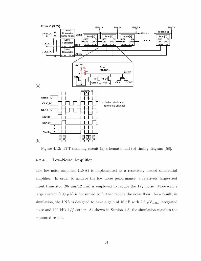
(a)
Scan[1]
CLK
ENCOUTCIN
RSTScan[2]
CLK
ENCOUTCIN
RSTScan[3]
CLK
ENCOUTCIN
RSTScan[7]
CLK
ENCOUTCIN
RST
GRSTL
CLKL
EN<1> EN<2> EN<3> EN<7>
GRST_IC
CLK_IC
CLKb_IC
GRST
CLK
CLKb
GRSTH
Level Converter
Level Converter
CLKHLevel
ConverterCLKL CLKH
CIN
Cint
RST CLK COUT
EN<N>
GRST GRST GRST GRST
From IC (3.6V)
EN<4>To RST[6]
35VFrom EN<N+1>
X
RL
GRST
(b)
CLK_IC
CLKb_IC
EN<1>
EN<2>
EN<7>
CH
2
CH
3
CH
8
CH
1C
H2
CH
3GRST_IC
Select dedicatedreference channel
1/20000 s
Figure 4.12: TFT scanning circuit (a) schematic and (b) timing diagram [58].
4.2.4.1 Low-Noise Amplifier
The low-noise amplifier (LNA) is implemented as a resistively loaded differential
amplifier. In order to achieve the low noise performance, a relatively large-sized
input transistor (96 μm/12 μm) is employed to reduce the 1/f noise. Moreover, a
large current (100 μA) is consumed to further reduce the noise floor. As a result, in
simulation, the LNA is designed to have a gain of 16 dB with 2.6 μVRMS integrated
noise and 100 kHz 1/f corner. As shown in Section 4.3, the simulation matches the
measured results.
61
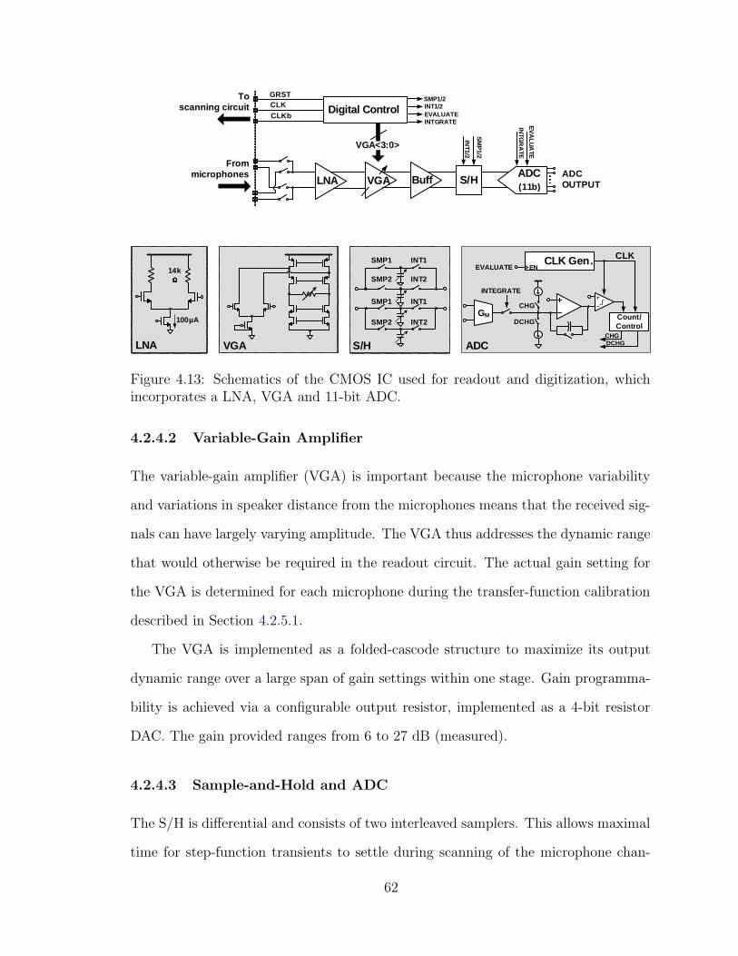
SMP1/2INT1/2
INTGRATEEVALUATE
GRSTCLKCLKb
VGA<3:0>
VGALNA
Digital ControlTo
scanning circuit
From microphones S/H
ADC OUTPUT
SM
P1/2
INT1/2
INTG
RA
TE
EV
ALU
ATE
BuffADC(11b)
LNA
14k
100 A
VGA
SMP1
SMP1
SMP2
SMP2
INT1
INT1
INT2
INT2
S/H
GM
INTEGRATE
Count/Control
CHG
DCHG
CLK
CHGDCHG
EVALUATECLK Gen.
EN
ADC
Figure 4.13: Schematics of the CMOS IC used for readout and digitization, whichincorporates a LNA, VGA and 11-bit ADC.
4.2.4.2 Variable-Gain Amplifier
The variable-gain amplifier (VGA) is important because the microphone variability
and variations in speaker distance from the microphones means that the received sig-
nals can have largely varying amplitude. The VGA thus addresses the dynamic range
that would otherwise be required in the readout circuit. The actual gain setting for
the VGA is determined for each microphone during the transfer-function calibration
described in Section 4.2.5.1.
The VGA is implemented as a folded-cascode structure to maximize its output
dynamic range over a large span of gain settings within one stage. Gain programma-
bility is achieved via a configurable output resistor, implemented as a 4-bit resistor
DAC. The gain provided ranges from 6 to 27 dB (measured).
4.2.4.3 Sample-and-Hold and ADC
The S/H is differential and consists of two interleaved samplers. This allows maximal
time for step-function transients to settle during scanning of the microphone chan-
62
nels and configuration of the VGA. Further, the hold capacitors are configurable,
implemented as 4-bit capacitor DACs. This, along with the VGA, allows the time
constant to adapt if increased scanning rates are desired (which would be required
to experiment with a number of sources N more than 2), while minimizing in-band
noise.
A buffer stage is inserted between VGA and S/H to decouple the VGAs resis-
tive load from the S/H’s capacitor, both of which are relatively large and varying.
Considering that the input for the buffer is already a relatively large signal after be-
ing amplified by the LNA and VGA, the buffer is implemented as a common source
amplifier with source degeneration to keep the linearity of the whole system while
providing another 7 dB gain.
Following the S/H is an integrating ADC, which digitizes the sample to 11b. A
transconductance stage (GM) generates a current signal, and a low-speed integrat-
ing op-amp circuit with switchable input current sources generates the dual slopes
required for data conversion via a digital counter. The integrating opamp is imple-
mented as a two-stage opamp with dominant pole compensation for stability.
4.2.5 Speech Separation Algorithm
The algorithm is divided into two steps. The first step consists of calibration, which
involves measuring the transfer functions between each source and each microphone.
The second step is reconstruction, which uses the previously measured transfer func-
tions to solve a system of equations and, thus, separate the two speech sources. Our
algorithm differs from prior work [47] by enabling us to critically sample our micro-
phone channels. We also expand upon previous work on critically sampled microphone
arrays, which assume only a single source is present, so they do not support source
separation [59].
63
4.2.5.1 Calibration
Calibration is used to measure the values of the transfer functions at every frequency
component required for reconstruction. This measurement is carried out using a cali-
bration signal, which has spectral content that covers all frequencies of interest. In a
practical application, this signal can be obtained by prompting users to speak one-by-
one in isolation. For the frequency band of interest (300 Hz to 5 kHz) measurements
of each transfer function can be done with a ∼100 ms window, since this a suitable
window length for estimating the transfer function when using speech [60]. A 7 s
speech signal was recorded for calibration. This corresponds to 1 s for each of the
seven channels, giving ample signal to identify a 100 ms window having high SNR
for estimating the transfer function from speech. Additionally, the absolute transfer
function with respect to each source is not required; this would be problematic to
measure since it would require recording at exactly the location of each source, in
order to de-embed the effect of sound propagation in the room. Instead, each transfer
function can be measured with respect to a designated reference channel within the
array.
When characterizing the transfer functions, Nyquist sampling of the microphones
is necessary (so that reconstruction can later be performed for each frequency bin
of the Nyquist-sampled source). Fig. 4.14 shows how this is achieved, along with
raw Nyquist samples from three representative channels. The system employs two
analog interfaces from LAE to CMOS for each sub-array. The reference channel is
provided continuously to the CMOS IC via a dedicated interface, while the remaining
channels are selected and characterized one at a time. This enables Nyquist-sampled
measurement of each channel, allowing each transfer function to be obtained with
respect to that of the reference channel.
64
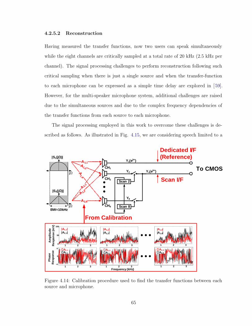
4.2.5.2 Reconstruction
Having measured the transfer functions, now two users can speak simultaneously
while the eight channels are critically sampled at a total rate of 20 kHz (2.5 kHz per
channel). The signal processing challenges to perform reconstruction following such
critical sampling when there is just a single source and when the transfer-function
to each microphone can be expressed as a simple time delay are explored in [59].
However, for the multi-speaker microphone system, additional challenges are raised
due to the simultaneous sources and due to the complex frequency dependencies of
the transfer functions from each source to each microphone.
The signal processing employed in this work to overcome these challenges is de-
scribed as follows. As illustrated in Fig. 4.15, we are considering speech limited to a
Am
plitu
de
Res
pons
e (m
V)
0
50
100
Pha
se
Res
pons
e
Frequency (kHz)
1 2 3 1 2 3 1 2 3
1 2 3 1 2 3 1 2 3
|A1,1||A2,1|
|A1,2||A2,2|
|A1,8||A2,8|
∠∠∠∠A1,1∠∠∠∠A2,1
∠∠∠∠A1,2∠∠∠∠A2,2
∠∠∠∠A1,8∠∠∠∠A2,8
-
0
CH1
CH8
Y8
|S1(j )|
j
|S2(j )|
jBW=10kHz
A1,1
A1,8
A2,8
A 2,1
• • •
Scan 2
Scan 8
Y1(ej )
Dedicated I/F (Reference)
CH2
Y2 Yx(ej )
Scan I/F
A1,2
A 2,2
To CMOS
From Calibration
Figure 4.14: Calibration procedure used to find the transfer functions between eachsource and microphone.
65
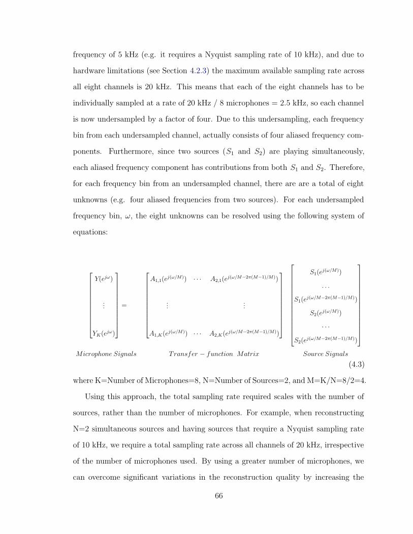
frequency of 5 kHz (e.g. it requires a Nyquist sampling rate of 10 kHz), and due to
hardware limitations (see Section 4.2.3) the maximum available sampling rate across
all eight channels is 20 kHz. This means that each of the eight channels has to be
individually sampled at a rate of 20 kHz / 8 microphones = 2.5 kHz, so each channel
is now undersampled by a factor of four. Due to this undersampling, each frequency
bin from each undersampled channel, actually consists of four aliased frequency com-
ponents. Furthermore, since two sources (S1 and S2) are playing simultaneously,
each aliased frequency component has contributions from both S1 and S2. Therefore,
for each frequency bin from an undersampled channel, there are are a total of eight
unknowns (e.g. four aliased frequencies from two sources). For each undersampled
frequency bin, ω, the eight unknowns can be resolved using the following system of
equations:
Y(ejω)
...
YK(ejω)
=
A1,1(ej(ω/M)) ∙ ∙ ∙ A2,1(e
j(ω/M−2π(M−1)/M))
......
A1,K(ej(ω/M)) ∙ ∙ ∙ A2,K(ej(ω/M−2π(M−1)/M))
S1(ej(ω/M))
. . .
S1(ej(ω/M−2π(M−1)/M))
S2(ej(ω/M))
∙ ∙ ∙
S2(ej(ω/M−2π(M−1)/M))
Microphone Signals Transfer − function Matrix Source Signals
(4.3)
where K=Number of Microphones=8, N=Number of Sources=2, and M=K/N=8/2=4.
Using this approach, the total sampling rate required scales with the number of
sources, rather than the number of microphones. For example, when reconstructing
N=2 simultaneous sources and having sources that require a Nyquist sampling rate
of 10 kHz, we require a total sampling rate across all channels of 20 kHz, irrespective
of the number of microphones used. By using a greater number of microphones, we
can overcome significant variations in the reconstruction quality by increasing the
66
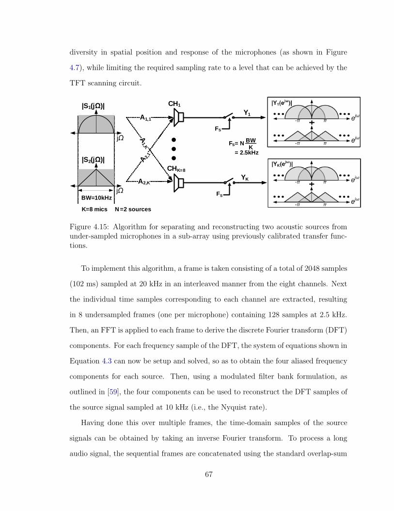
diversity in spatial position and response of the microphones (as shown in Figure
4.7), while limiting the required sampling rate to a level that can be achieved by the
TFT scanning circuit.
CH1
CHK=8
Y1
YK
|S1(j )|
j
|S2(j )|
jBW=10kHz
A1,1
A1,K
A2,K
A 2,1
• • •
FS= N BWK
= 2.5kHz
FS
FS
K=8 mics N =2 sources
Figure 4.15: Algorithm for separating and reconstructing two acoustic sources fromunder-sampled microphones in a sub-array using previously calibrated transfer func-tions.
To implement this algorithm, a frame is taken consisting of a total of 2048 samples
(102 ms) sampled at 20 kHz in an interleaved manner from the eight channels. Next
the individual time samples corresponding to each channel are extracted, resulting
in 8 undersampled frames (one per microphone) containing 128 samples at 2.5 kHz.
Then, an FFT is applied to each frame to derive the discrete Fourier transform (DFT)
components. For each frequency sample of the DFT, the system of equations shown in
Equation 4.3 can now be setup and solved, so as to obtain the four aliased frequency
components for each source. Then, using a modulated filter bank formulation, as
outlined in [59], the four components can be used to reconstruct the DFT samples of
the source signal sampled at 10 kHz (i.e., the Nyquist rate).
Having done this over multiple frames, the time-domain samples of the source
signals can be obtained by taking an inverse Fourier transform. To process a long
audio signal, the sequential frames are concatenated using the standard overlap-sum
67
technique [61]. Each frame is overlapped by 75% with the preceding frame, so as
to ensure it meets the constant overlap-add condition for the Hann windows used in
order to mitigate artifacts [62].
4.3 Prototype Measurements and System Demo
Fig. 4.16 shows the prototype of the whole system, including LAE components and
CMOS IC. The PVDF thin-film microphones, and the a-Si TFT amplifiers and scan-
ning circuits deposited at 180 ◦C on a glass substrate, were all produced in-house.
Within a large-area system, these can be thought of as comprising the front plane and
back plane, respectively [1], and various methods of fabricating front planes consist-
ing of microphone arrays have been considered [63].The CMOS IC was implemented
in a 130-nm technology from IBM. The microphone sub-array spanned a width of
105 cm, and consisted of eight PVDF microphones, approximately spaced by 15 cm.
These technologies were selected due to their proven robustness; however, the hybrid
LAE-CMOS architecture presented can be readily adapted to different CMOS process
nodes and TFT transistor technologies.
Table 4.3 provides a measurement summary of all the system components. On
the LAE side, each local amplifier channel consumes 3.5 mW and the scanning circuit
for each sub-array consumes 12 mW. The CMOS readout IC consumes 0.6 mW in
total. Fig. 4.17 shows details from characterization of the TFT amplifier (left) and
the CMOS readout circuit (right). The bandwidth (pass-band is from 0.3 to 3 kHz)
of the TFT amplifier is tuned to match human speech, and filter out-of-band noise.
Its CMRR of 49 dB is limited by the mismatch of the TFTs. Nevertheless, as shown
in the waveforms, it substantially suppresses stray common-mode noise. The CMOS
readout circuit successfully achieves programmable gain from 16 to 43 dB overall.
The CMRR and linearity measurements are also shown.
68
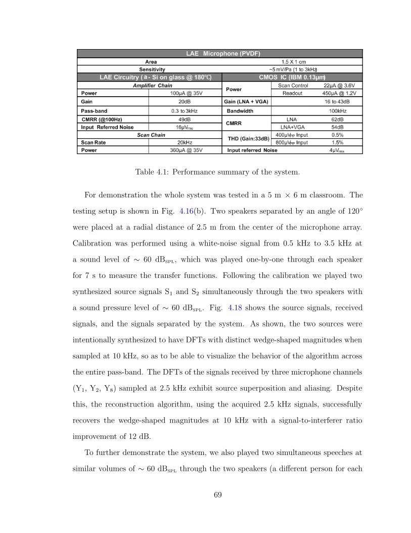
Table 4.1: Performance summary of the system.
For demonstration the whole system was tested in a 5 m × 6 m classroom. The
testing setup is shown in Fig. 4.16(b). Two speakers separated by an angle of 120◦
were placed at a radial distance of 2.5 m from the center of the microphone array.
Calibration was performed using a white-noise signal from 0.5 kHz to 3.5 kHz at
a sound level of ∼ 60 dBSPL, which was played one-by-one through each speaker
for 7 s to measure the transfer functions. Following the calibration we played two
synthesized source signals S1 and S2 simultaneously through the two speakers with
a sound pressure level of ∼ 60 dBSPL. Fig. 4.18 shows the source signals, received
signals, and the signals separated by the system. As shown, the two sources were
intentionally synthesized to have DFTs with distinct wedge-shaped magnitudes when
sampled at 10 kHz, so as to be able to visualize the behavior of the algorithm across
the entire pass-band. The DFTs of the signals received by three microphone channels
(Y1, Y2, Y8) sampled at 2.5 kHz exhibit source superposition and aliasing. Despite
this, the reconstruction algorithm, using the acquired 2.5 kHz signals, successfully
recovers the wedge-shaped magnitudes at 10 kHz with a signal-to-interferer ratio
improvement of 12 dB.
To further demonstrate the system, we also played two simultaneous speeches at
similar volumes of ∼ 60 dBSPL through the two speakers (a different person for each
69
speaker). Fig. 4.19 shows the time-domain waveforms of the signal received by the
first microphone channel (this corresponds to microphone at center of the array and
is used as a reference channel for defining time delays, as described in Section 4.2.5.1)
and those separated by the system (with the original signal waveforms overlayed). As
seen, the two distinct input signals are successfully separated at the output, corre-
sponding to a signal-to-interferer improvement of 11 dB. The reconstructed speech of
each speaker is clear and intelligible, and prepares them for further speech-recognition
processing within applications. The small residual difference between the original and
reconstructed signals is primarily due to inaccuracies in transfer-function calibration,
leading to errors in the reconstruction of certain signal frequency components.
4.4 Conclusion
Multi-speaker voice separation will enable collaborative control of ambient electronic
devices. This chapter addresses this application by demonstrating a hybrid system
for speech separation, which is based on combining LAE and a CMOS IC. In this
chapter we: (1) develop an LAE microphone array, based on PVDF microphones and
a-Si TFT instrumentation, which we integrate with a CMOS IC for audio readout;
(2) develop an algorithm for source separation, which overcomes the large variability
of the PVDF microphones and the sampling rate limitations of the TFT circuits; (3)
demonstrate an eight-channel sub-array system, spanning the entire signal chain from
the transducer to digitization, which successfully separates two simultaneous audio
sources.
4.5 Acknowledgments
The entirety of CMOS IC was designed and characterized by Liechao Huang. He and
the author also closely collaborated when integrating the LAE amplifiers with the
70

CMOS IC. The PVDF microphone fabrication process was refined, and techniques
for optimizing the the frequency response were developed by Richard Cheng. The
large-area scanning circuit was designed and characterized by Tiffany Moy.
71
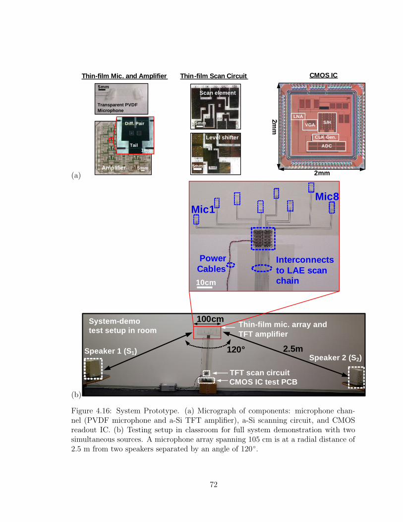
(a)
Thin-film Mic. and Amplifier Thin-film Scan Circuit CMOS IC
Scan element
5mm
Level shifter
5mm
LNA
VGA S/H
ADC
CLK Gen.
2mm
2mm
Transparent PVDFMicrophone
5mm
Diff. Pair
1mmTail
5mmAmplifier
(b)
Interconnectsto LAE scan chain
Mic1Mic8
PowerCables
10cm
Speaker 1 (S 1)Speaker 2 (S 2)
CMOS IC test PCB
2.5m120°
TFT scan circuit
System-demo test setup in room
Thin-film mic. array and TFT amplifier
100cm
Figure 4.16: System Prototype. (a) Micrograph of components: microphone chan-nel (PVDF microphone and a-Si TFT amplifier), a-Si scanning circuit, and CMOSreadout IC. (b) Testing setup in classroom for full system demonstration with twosimultaneous sources. A microphone array spanning 105 cm is at a radial distance of2.5 m from two speakers separated by an angle of 120◦.
72
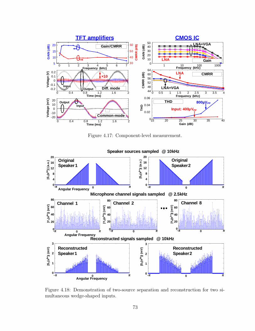
0 1 2 3 4 5 6 75
10
15
20
Frequency (kHz)
40
50
30
60
CM
RR
(dB
)
GA
IN(d
B)
-20-10
01020
0 0.4 0.8 1.2 1.6 2-0.2-0.1
00.10.2
Vol
tag
e (V
)V
olta
ge (
mV
)
0 0.4 0.8 1.2 1.6 2
Time (ms)
Time (ms)
TFT amplifiers
×10
CM
RR
(dB
)
Frequency (kHz)0 0.5 1 1.5 2 2.5 3 3.5 444
4852566064
LNA
LNA+VGA
15 20 25 30 35 400
0.02
0.04
0.06
TH
D
Gain (dB)
800µVPP
Input: 400µV PP
GA
IN (
dB)
Frequency (kHz)
LNA
CMOS ICLNA+VGA
Diff. mode
Common-mode
InputOutput
OutputInput
CMRR
THD
Gain/CMRR
1 10 100 10000
1020304050
Gain
Figure 4.17: Component-level measurement.
0
20
40
60
80
|Y1(
ej)|
(mV
)
0- 0
20
40
60
80
0- 0
20
40
60
80
0-
|Y2(
ej
)| (
mV
)
|Y8(
ej
)| (m
V)
00
4
8
12
16
20
|S1(
ej
)| (a
.u.)
|S2(
ej)|
(a.u
.)
0
4
8
12
16
20
- 0-
0
1
2
3
|S1(
ej)|
(mV
)
0-0- 0
1
2
3
|S2(
ej)|
(m
V)
Speaker sources sampled @ 10kHz
Microphone channel signals sampled @ 2.5kHz
Reconstructed signals sampled @ 10kHz
OriginalSpeaker 1
OriginalSpeaker2
Channel 1 Channel 2 Channel 8
ReconstructedSpeaker1
ReconstructedSpeaker2
Angular Frequency
Angular Frequency
Angular Frequency
Figure 4.18: Demonstration of two-source separation and reconstruction for two si-multaneous wedge-shaped inputs.
73
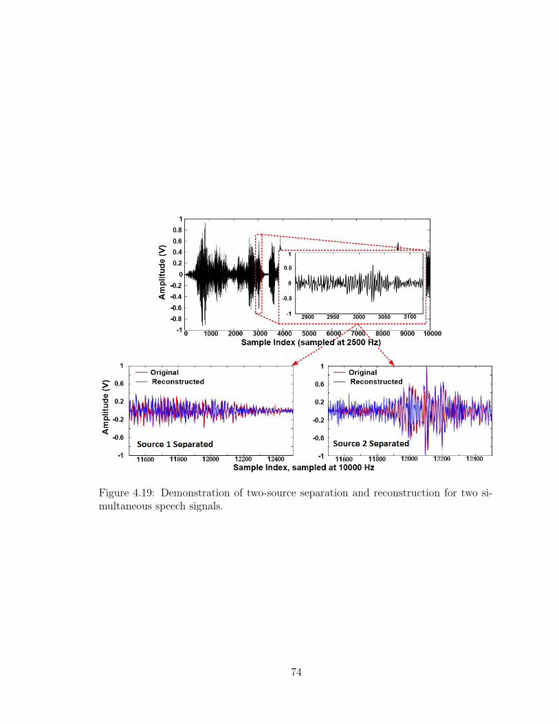
Figure 4.19: Demonstration of two-source separation and reconstruction for two si-multaneous speech signals.
74
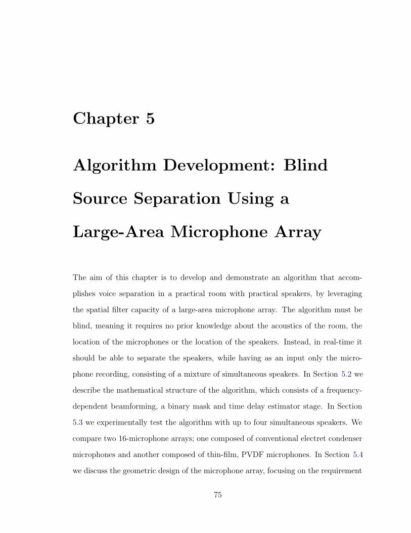
Chapter 5
Algorithm Development: Blind
Source Separation Using a
Large-Area Microphone Array
The aim of this chapter is to develop and demonstrate an algorithm that accom-
plishes voice separation in a practical room with practical speakers, by leveraging
the spatial filter capacity of a large-area microphone array. The algorithm must be
blind, meaning it requires no prior knowledge about the acoustics of the room, the
location of the microphones or the location of the speakers. Instead, in real-time it
should be able to separate the speakers, while having as an input only the micro-
phone recording, consisting of a mixture of simultaneous speakers. In Section 5.2 we
describe the mathematical structure of the algorithm, which consists of a frequency-
dependent beamforming, a binary mask and time delay estimator stage. In Section
5.3 we experimentally test the algorithm with up to four simultaneous speakers. We
compare two 16-microphone arrays; one composed of conventional electret condenser
microphones and another composed of thin-film, PVDF microphones. In Section 5.4
we discuss the geometric design of the microphone array, focusing on the requirement
75