Embed Size (px)
Citation preview
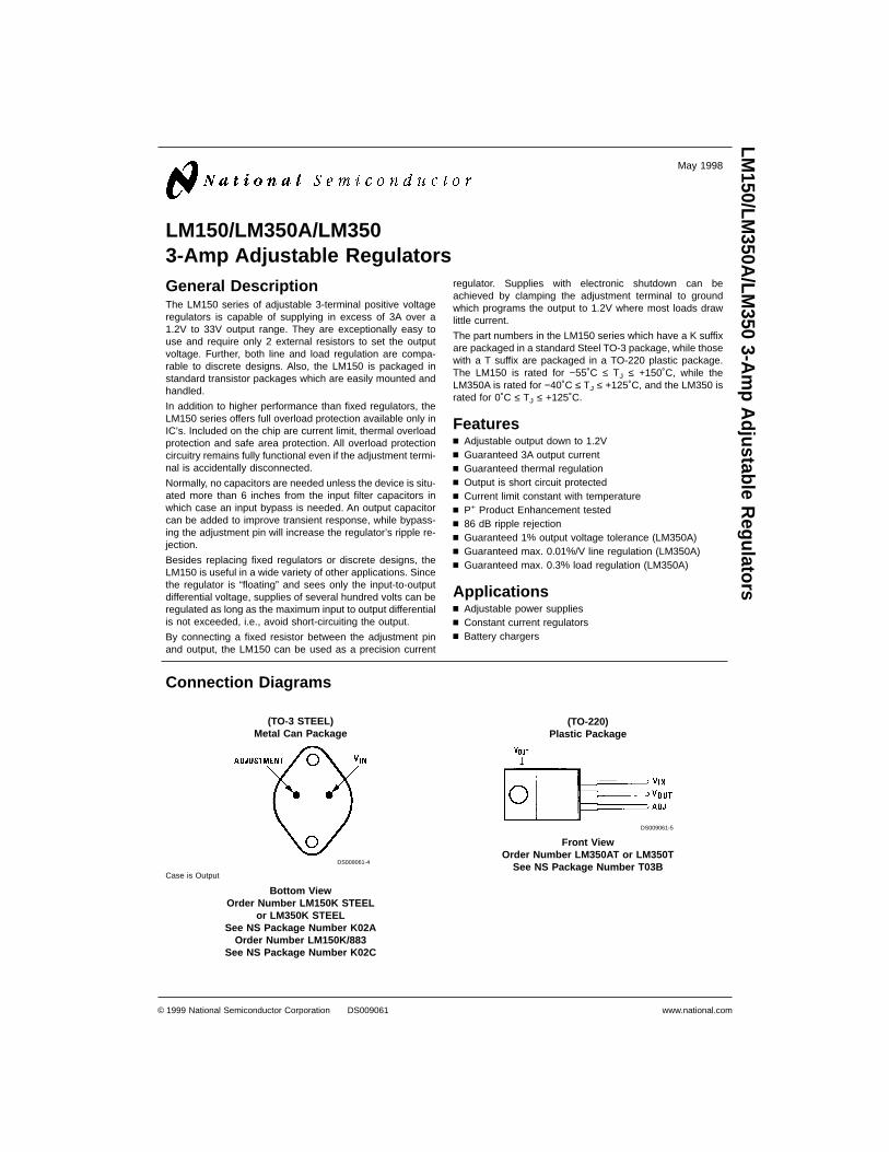
LM150/LM350A/LM3503-Amp Adjustable RegulatorsGeneral DescriptionThe LM150 series of adjustable 3-terminal positive voltageregulators is capable of supplying in excess of 3A over a1.2V to 33V output range. They are exceptionally easy touse and require only 2 external resistors to set the outputvoltage. Further, both line and load regulation are compa-rable to discrete designs. Also, the LM150 is packaged instandard transistor packages which are easily mounted andhandled.
In addition to higher performance than fixed regulators, theLM150 series offers full overload protection available only inIC’s. Included on the chip are current limit, thermal overloadprotection and safe area protection. All overload protectioncircuitry remains fully functional even if the adjustment termi-nal is accidentally disconnected.
Normally, no capacitors are needed unless the device is situ-ated more than 6 inches from the input filter capacitors inwhich case an input bypass is needed. An output capacitorcan be added to improve transient response, while bypass-ing the adjustment pin will increase the regulator’s ripple re-jection.
Besides replacing fixed regulators or discrete designs, theLM150 is useful in a wide variety of other applications. Sincethe regulator is “floating” and sees only the input-to-outputdifferential voltage, supplies of several hundred volts can beregulated as long as the maximum input to output differentialis not exceeded, i.e., avoid short-circuiting the output.
By connecting a fixed resistor between the adjustment pinand output, the LM150 can be used as a precision current
regulator. Supplies with electronic shutdown can beachieved by clamping the adjustment terminal to groundwhich programs the output to 1.2V where most loads drawlittle current.
The part numbers in the LM150 series which have a K suffixare packaged in a standard Steel TO-3 package, while thosewith a T suffix are packaged in a TO-220 plastic package.The LM150 is rated for −55˚C ≤ TJ ≤ +150˚C, while theLM350A is rated for −40˚C ≤ TJ ≤ +125˚C, and the LM350 israted for 0˚C ≤ TJ ≤ +125˚C.
Featuresn Adjustable output down to 1.2Vn Guaranteed 3A output currentn Guaranteed thermal regulationn Output is short circuit protectedn Current limit constant with temperaturen P+ Product Enhancement testedn 86 dB ripple rejectionn Guaranteed 1% output voltage tolerance (LM350A)n Guaranteed max. 0.01%/V line regulation (LM350A)n Guaranteed max. 0.3% load regulation (LM350A)
Applicationsn Adjustable power suppliesn Constant current regulatorsn Battery chargers
Connection Diagrams
(TO-3 STEEL)Metal Can Package
DS009061-4
Case is Output
Bottom ViewOrder Number LM150K STEEL
or LM350K STEELSee NS Package Number K02A
Order Number LM150K/883See NS Package Number K02C
(TO-220)Plastic Package
DS009061-5
Front ViewOrder Number LM350AT or LM350T
See NS Package Number T03B
May 1998
LM150/LM
350A/LM
3503-A
mp
Adjustable
Regulators
© 1999 National Semiconductor Corporation DS009061 www.national.com
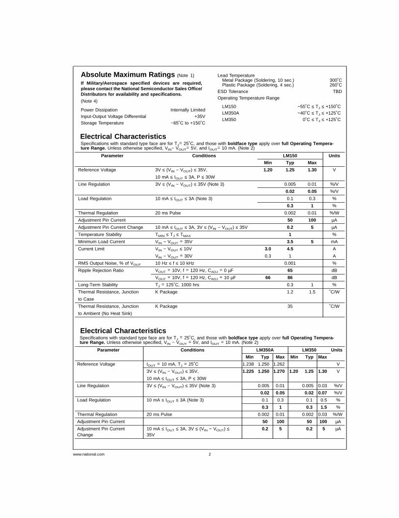
Absolute Maximum Ratings (Note 1)
If Military/Aerospace specified devices are required,please contact the National Semiconductor Sales Office/Distributors for availability and specifications.
(Note 4)
Power Dissipation Internally LimitedInput-Output Voltage Differential +35VStorage Temperature −65˚C to +150˚C
Lead TemperatureMetal Package (Soldering, 10 sec.)Plastic Package (Soldering, 4 sec.)
300˚C260˚C
ESD Tolerance TBDOperating Temperature Range
LM150 −55˚C ≤ TJ ≤ +150˚CLM350A −40˚C ≤ TJ ≤ +125˚CLM350 0˚C ≤ TJ ≤ +125˚C
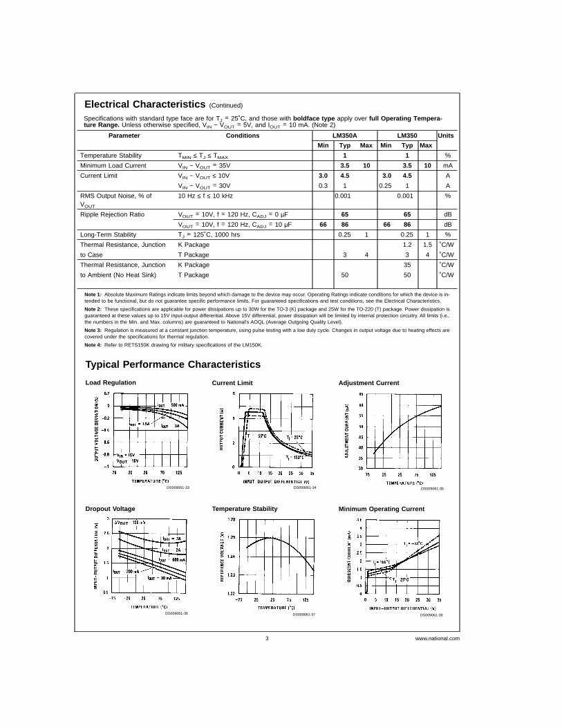
Electrical CharacteristicsSpecifications with standard type face are for TJ= 25˚C, and those with boldface type apply over full Operating Tempera-ture Range. Unless otherwise specified, VIN− VOUT= 5V, and IOUT= 10 mA. (Note 2)
Parameter Conditions LM150 Units
Min Typ Max
Reference Voltage 3V ≤ (VIN − VOUT) ≤ 35V, 1.20 1.25 1.30 V
10 mA ≤ IOUT ≤ 3A, P ≤ 30W
Line Regulation 3V ≤ (VIN − VOUT) ≤ 35V (Note 3) 0.005 0.01 %/V
0.02 0.05 %/V
Load Regulation 10 mA ≤ IOUT ≤ 3A (Note 3) 0.1 0.3 %
0.3 1 %
Thermal Regulation 20 ms Pulse 0.002 0.01 %/W
Adjustment Pin Current 50 100 µA
Adjustment Pin Current Change 10 mA ≤ IOUT ≤ 3A, 3V ≤ (VIN − VOUT) ≤ 35V 0.2 5 µA
Temperature Stability TMIN ≤ TJ ≤ TMAX 1 %
Minimum Load Current VIN − VOUT = 35V 3.5 5 mA
Current Limit VIN − VOUT ≤ 10V 3.0 4.5 A
VIN − VOUT = 30V 0.3 1 A
RMS Output Noise, % of VOUT 10 Hz ≤ f ≤ 10 kHz 0.001 %
Ripple Rejection Ratio VOUT = 10V, f = 120 Hz, CADJ = 0 µF 65 dB
VOUT = 10V, f = 120 Hz, CADJ = 10 µF 66 86 dB
Long-Term Stability TJ = 125˚C, 1000 hrs 0.3 1 %
Thermal Resistance, Junction K Package 1.2 1.5 ˚C/W
to Case
Thermal Resistance, Junction K Package 35 ˚C/W
to Ambient (No Heat Sink)
Electrical CharacteristicsSpecifications with standard type face are for TJ = 25˚C, and those with boldface type apply over full Operating Tempera-ture Range. Unless otherwise specified, VIN − VOUT = 5V, and IOUT = 10 mA. (Note 2)
Parameter Conditions LM350A LM350 Units
Min Typ Max Min Typ Max
Reference Voltage IOUT = 10 mA, TJ = 25˚C 1.238 1.250 1.262 V
3V ≤ (VIN − VOUT) ≤ 35V, 1.225 1.250 1.270 1.20 1.25 1.30 V
10 mA ≤ IOUT ≤ 3A, P ≤ 30W
Line Regulation 3V ≤ (VIN − VOUT) ≤ 35V (Note 3) 0.005 0.01 0.005 0.03 %/V
0.02 0.05 0.02 0.07 %/V
Load Regulation 10 mA ≤ IOUT ≤ 3A (Note 3) 0.1 0.3 0.1 0.5 %
0.3 1 0.3 1.5 %
Thermal Regulation 20 ms Pulse 0.002 0.01 0.002 0.03 %/W
Adjustment Pin Current 50 100 50 100 µA
Adjustment Pin CurrentChange
10 mA ≤ IOUT ≤ 3A, 3V ≤ (VIN − VOUT) ≤35V
0.2 5 0.2 5 µA
www.national.com 2
Electrical Characteristics (Continued)
Specifications with standard type face are for TJ = 25˚C, and those with boldface type apply over full Operating Tempera-ture Range. Unless otherwise specified, VIN − VOUT = 5V, and IOUT = 10 mA. (Note 2)
Parameter Conditions LM350A LM350 Units
Min Typ Max Min Typ Max
Temperature Stability TMIN ≤ TJ ≤ TMAX 1 1 %
Minimum Load Current VIN − VOUT = 35V 3.5 10 3.5 10 mA
Current Limit VIN − VOUT ≤ 10V 3.0 4.5 3.0 4.5 A
VIN − VOUT = 30V 0.3 1 0.25 1 A
RMS Output Noise, % ofVOUT
10 Hz ≤ f ≤ 10 kHz 0.001 0.001 %
Ripple Rejection Ratio VOUT = 10V, f = 120 Hz, CADJ = 0 µF 65 65 dB
VOUT = 10V, f = 120 Hz, CADJ = 10 µF 66 86 66 86 dB
Long-Term Stability TJ = 125˚C, 1000 hrs 0.25 1 0.25 1 %
Thermal Resistance, Junction K Package 1.2 1.5 ˚C/W
to Case T Package 3 4 3 4 ˚C/W
Thermal Resistance, Junction K Package 35 ˚C/W
to Ambient (No Heat Sink) T Package 50 50 ˚C/W
Note 1: Absolute Maximum Ratings indicate limits beyond which damage to the device may occur. Operating Ratings indicate conditions for which the device is in-tended to be functional, but do not guarantee specific performance limits. For guaranteed specifications and test conditions, see the Electrical Characteristics.
Note 2: These specifications are applicable for power dissipations up to 30W for the TO-3 (K) package and 25W for the TO-220 (T) package. Power dissipation isguaranteed at these values up to 15V input-output differential. Above 15V differential, power dissipation will be limited by internal protection circuitry. All limits (i.e.,the numbers in the Min. and Max. columns) are guaranteed to National’s AOQL (Average Outgoing Quality Level).
Note 3: Regulation is measured at a constant junction temperature, using pulse testing with a low duty cycle. Changes in output voltage due to heating effects arecovered under the specifications for thermal regulation.
Note 4: Refer to RETS150K drawing for military specifications of the LM150K.
Typical Performance Characteristics
Load Regulation
DS009061-33
Current Limit
DS009061-34
Adjustment Current
DS009061-35
Dropout Voltage
DS009061-36
Temperature Stability
DS009061-37
Minimum Operating Current
DS009061-38
www.national.com3
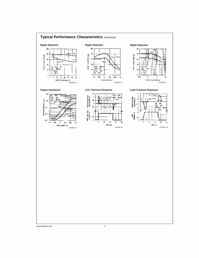
Typical Performance Characteristics (Continued)
Ripple Rejection
DS009061-39
Ripple Rejection
DS009061-40
Ripple Rejection
DS009061-41
Output Impedance
DS009061-42
Line Transient Response
DS009061-43
Load Transient Response
DS009061-44
www.national.com 4
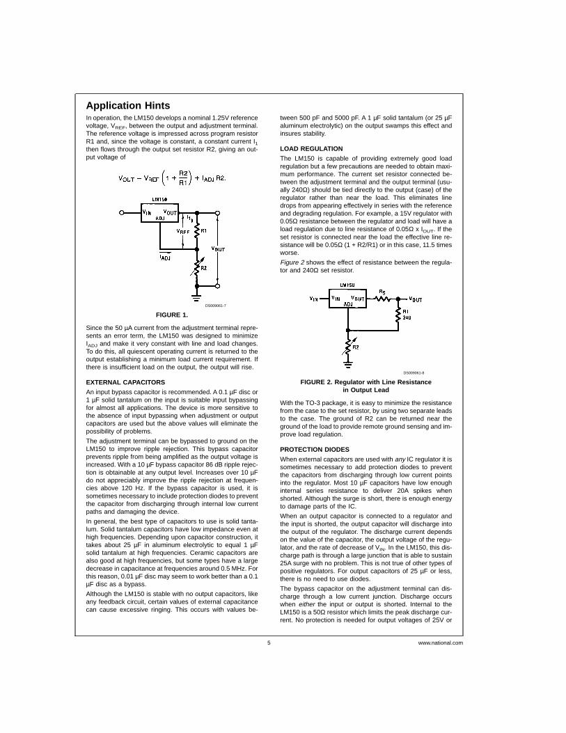
Application HintsIn operation, the LM150 develops a nominal 1.25V referencevoltage, VREF, between the output and adjustment terminal.The reference voltage is impressed across program resistorR1 and, since the voltage is constant, a constant current I1then flows through the output set resistor R2, giving an out-put voltage of
Since the 50 µA current from the adjustment terminal repre-sents an error term, the LM150 was designed to minimizeIADJ and make it very constant with line and load changes.To do this, all quiescent operating current is returned to theoutput establishing a minimum load current requirement. Ifthere is insufficient load on the output, the output will rise.
EXTERNAL CAPACITORS
An input bypass capacitor is recommended. A 0.1 µF disc or1 µF solid tantalum on the input is suitable input bypassingfor almost all applications. The device is more sensitive tothe absence of input bypassing when adjustment or outputcapacitors are used but the above values will eliminate thepossibility of problems.
The adjustment terminal can be bypassed to ground on theLM150 to improve ripple rejection. This bypass capacitorprevents ripple from being amplified as the output voltage isincreased. With a 10 µF bypass capacitor 86 dB ripple rejec-tion is obtainable at any output level. Increases over 10 µFdo not appreciably improve the ripple rejection at frequen-cies above 120 Hz. If the bypass capacitor is used, it issometimes necessary to include protection diodes to preventthe capacitor from discharging through internal low currentpaths and damaging the device.
In general, the best type of capacitors to use is solid tanta-lum. Solid tantalum capacitors have low impedance even athigh frequencies. Depending upon capacitor construction, ittakes about 25 µF in aluminum electrolytic to equal 1 µFsolid tantalum at high frequencies. Ceramic capacitors arealso good at high frequencies, but some types have a largedecrease in capacitance at frequencies around 0.5 MHz. Forthis reason, 0.01 µF disc may seem to work better than a 0.1µF disc as a bypass.
Although the LM150 is stable with no output capacitors, likeany feedback circuit, certain values of external capacitancecan cause excessive ringing. This occurs with values be-
tween 500 pF and 5000 pF. A 1 µF solid tantalum (or 25 µFaluminum electrolytic) on the output swamps this effect andinsures stability.
LOAD REGULATION
The LM150 is capable of providing extremely good loadregulation but a few precautions are needed to obtain maxi-mum performance. The current set resistor connected be-tween the adjustment terminal and the output terminal (usu-ally 240Ω) should be tied directly to the output (case) of theregulator rather than near the load. This eliminates linedrops from appearing effectively in series with the referenceand degrading regulation. For example, a 15V regulator with0.05Ω resistance between the regulator and load will have aload regulation due to line resistance of 0.05Ω x IOUT. If theset resistor is connected near the load the effective line re-sistance will be 0.05Ω (1 + R2/R1) or in this case, 11.5 timesworse.
Figure 2 shows the effect of resistance between the regula-tor and 240Ω set resistor.
With the TO-3 package, it is easy to minimize the resistancefrom the case to the set resistor, by using two separate leadsto the case. The ground of R2 can be returned near theground of the load to provide remote ground sensing and im-prove load regulation.
PROTECTION DIODES
When external capacitors are used with any IC regulator it issometimes necessary to add protection diodes to preventthe capacitors from discharging through low current pointsinto the regulator. Most 10 µF capacitors have low enoughinternal series resistance to deliver 20A spikes whenshorted. Although the surge is short, there is enough energyto damage parts of the IC.
When an output capacitor is connected to a regulator andthe input is shorted, the output capacitor will discharge intothe output of the regulator. The discharge current dependson the value of the capacitor, the output voltage of the regu-lator, and the rate of decrease of VIN. In the LM150, this dis-charge path is through a large junction that is able to sustain25A surge with no problem. This is not true of other types ofpositive regulators. For output capacitors of 25 µF or less,there is no need to use diodes.
The bypass capacitor on the adjustment terminal can dis-charge through a low current junction. Discharge occurswhen either the input or output is shorted. Internal to theLM150 is a 50Ω resistor which limits the peak discharge cur-rent. No protection is needed for output voltages of 25V or
DS009061-7
FIGURE 1.
DS009061-8
FIGURE 2. Regulator with Line Resistancein Output Lead
www.national.com5
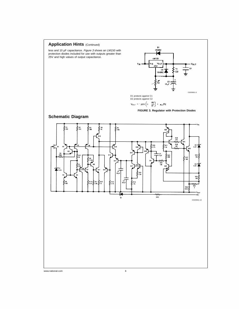
Application Hints (Continued)
less and 10 µF capacitance. Figure 3 shows an LM150 withprotection diodes included for use with outputs greater than25V and high values of output capacitance.
Schematic Diagram
DS009061-9
D1 protects against C1D2 protects against C2
FIGURE 3. Regulator with Protection Diodes
DS009061-10
www.national.com 6
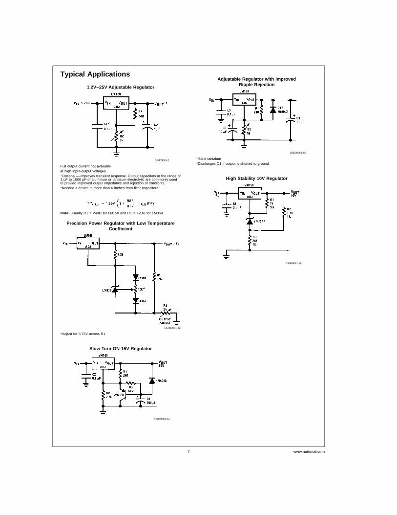
Typical Applications
Note: Usually R1 = 240Ω for LM150 and R1 = 120Ω for LM350.
1.2V–25V Adjustable Regulator
DS009061-1
Full output current not availableat high input-output voltages.†Optional — improves transient response. Output capacitors in the range of1 µF to 1000 µF of aluminum or tantalum electrolytic are commonly usedto provide improved output impedance and rejection of transients.*Needed if device is more than 6 inches from filter capacitors.
Precision Power Regulator with Low TemperatureCoefficient
DS009061-13
*Adjust for 3.75V across R1
Slow Turn-ON 15V Regulator
DS009061-14
Adjustable Regulator with ImprovedRipple Rejection
DS009061-15
†Solid tantalum*Discharges C1 if output is shorted to ground
High Stability 10V Regulator
DS009061-16
www.national.com7

Typical Applications (Continued)
Digitally Selected Outputs
DS009061-17
*Sets maximum VOUT
Regulator and Voltage Reference
DS009061-3
10A Regulator
DS009061-18
*Minimum load current 50 mA
www.national.com 8
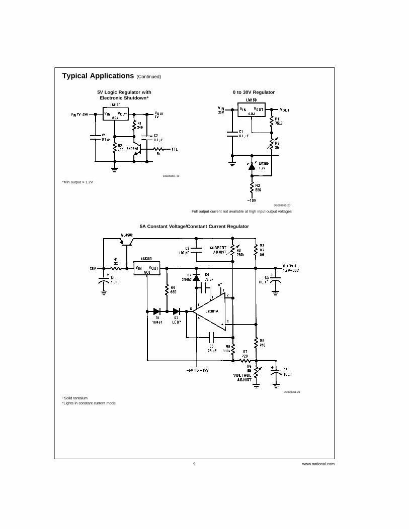
Typical Applications (Continued)
5V Logic Regulator withElectronic Shutdown *
DS009061-19
*Min output ≈ 1.2V
0 to 30V Regulator
DS009061-20
Full output current not available at high input-output voltages
5A Constant Voltage/Constant Current Regulator
DS009061-21
†Solid tantalum*Lights in constant current mode
www.national.com9
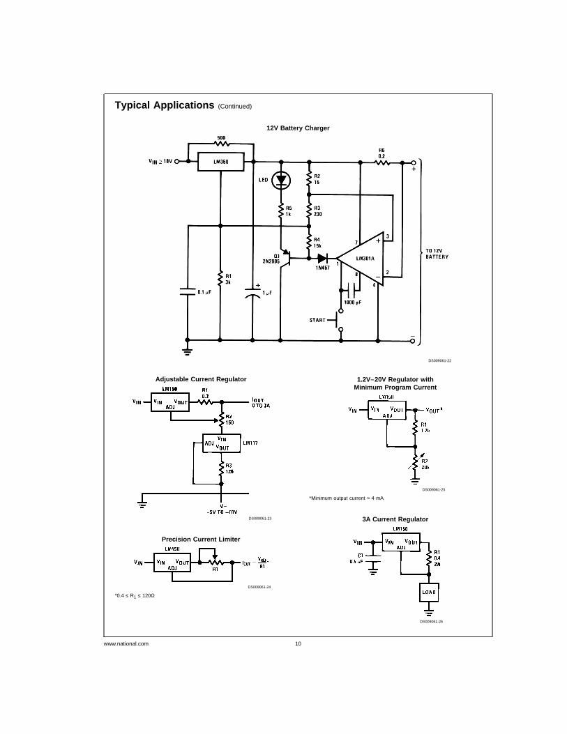
Typical Applications (Continued)
12V Battery Charger
DS009061-22
Adjustable Current Regulator
DS009061-23
Precision Current Limiter
DS009061-24
*0.4 ≤ R1 ≤ 120Ω
1.2V–20V Regulator withMinimum Program Current
DS009061-25
*Minimum output current ≈ 4 mA
3A Current Regulator
DS009061-26
www.national.com 10
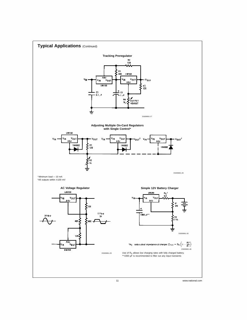
Typical Applications (Continued)
Tracking Preregulator
DS009061-27
Adjusting Multiple On-Card Regulatorswith Single Control *
DS009061-28
†Minimum load — 10 mA*All outputs within ±100 mV
AC Voltage Regulator
DS009061-29
Simple 12V Battery Charger
DS009061-30
DS009061-48
Use of RS allows low charging rates with fully charged battery.**1000 µF is recommended to filter out any input transients
www.national.com11
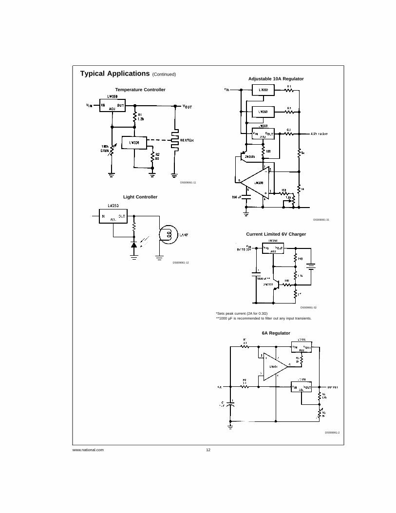
Typical Applications (Continued)
Temperature Controller
DS009061-11
Light Controller
DS009061-12
Adjustable 10A Regulator
DS009061-31
Current Limited 6V Charger
DS009061-32
*Sets peak current (2A for 0.3Ω)**1000 µF is recommended to filter out any input transients.
6A Regulator
DS009061-2
www.national.com 12
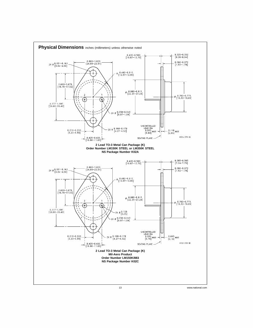
Physical Dimensions inches (millimeters) unless otherwise noted
2 Lead TO-3 Metal Can Package (K)Order Number LM150K STEEL or LM350K STEEL
NS Package Number K02A
2 Lead TO-3 Metal Can Package (K)Mil-Aero Product
Order Number LM150K/883NS Package Number K02C
www.national.com13
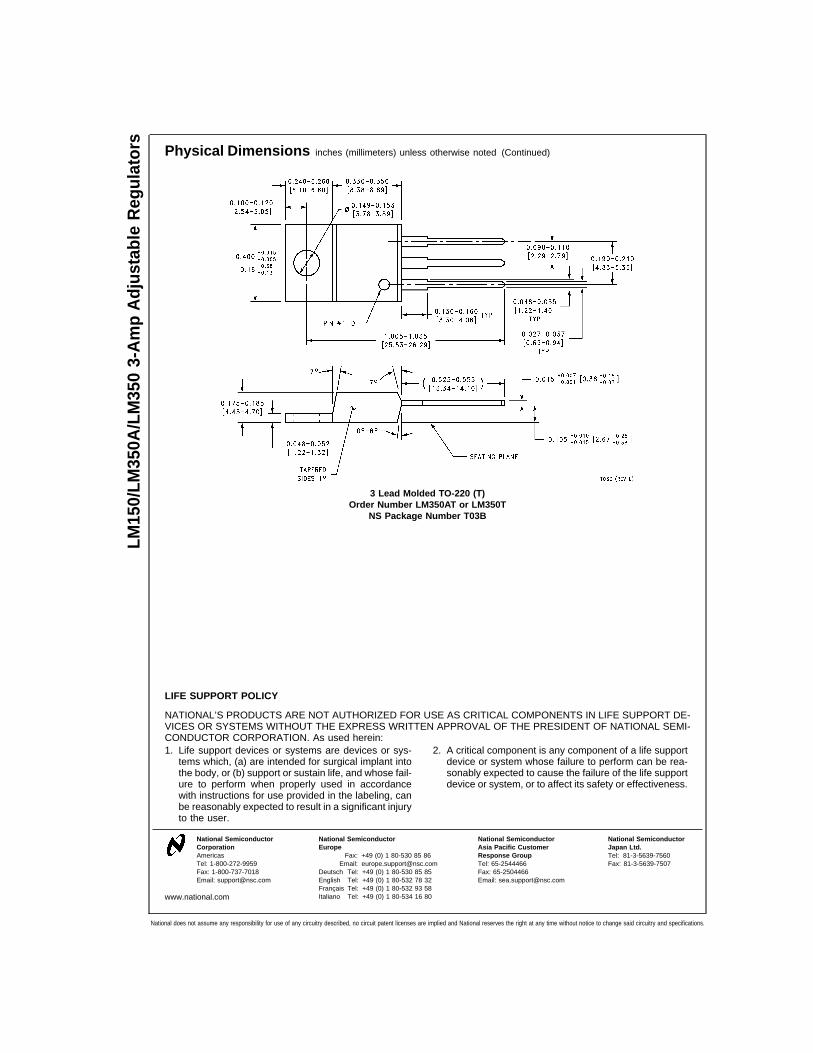
Physical Dimensions inches (millimeters) unless otherwise noted (Continued)
LIFE SUPPORT POLICY
NATIONAL’S PRODUCTS ARE NOT AUTHORIZED FOR USE AS CRITICAL COMPONENTS IN LIFE SUPPORT DE-VICES OR SYSTEMS WITHOUT THE EXPRESS WRITTEN APPROVAL OF THE PRESIDENT OF NATIONAL SEMI-CONDUCTOR CORPORATION. As used herein:1. Life support devices or systems are devices or sys-
tems which, (a) are intended for surgical implant intothe body, or (b) support or sustain life, and whose fail-ure to perform when properly used in accordancewith instructions for use provided in the labeling, canbe reasonably expected to result in a significant injuryto the user.
2. A critical component is any component of a life supportdevice or system whose failure to perform can be rea-sonably expected to cause the failure of the life supportdevice or system, or to affect its safety or effectiveness.
National SemiconductorCorporationAmericasTel: 1-800-272-9959Fax: 1-800-737-7018Email: [email protected]
www.national.com
National SemiconductorEurope
Fax: +49 (0) 1 80-530 85 86Email: [email protected]
Deutsch Tel: +49 (0) 1 80-530 85 85English Tel: +49 (0) 1 80-532 78 32Français Tel: +49 (0) 1 80-532 93 58Italiano Tel: +49 (0) 1 80-534 16 80
National SemiconductorAsia Pacific CustomerResponse GroupTel: 65-2544466Fax: 65-2504466Email: [email protected]
National SemiconductorJapan Ltd.Tel: 81-3-5639-7560Fax: 81-3-5639-7507
3 Lead Molded TO-220 (T)Order Number LM350AT or LM350T
NS Package Number T03B
LM15
0/LM
350A
/LM
350
3-A
mp
Adj
usta
ble
Reg
ulat
ors
National does not assume any responsibility for use of any circuitry described, no circuit patent licenses are implied and National reserves the right at any time without notice to change said circuitry and specifications.