Embed Size (px)
Citation preview
TL/H/9139
LM
1801
Batte
ryO
pera
ted
Pow
erC
om
para
tor
February 1995
LM1801 Battery Operated Power Comparator
General DescriptionThe LM1801 is an extremely low power comparator with a
high current, open-collector output stage. The typical supply
current is only 7 mA, yet in its switched state the comparator
can source or sink 0.5A. The LM1801 is designed to oper-
ate in a standby mode for 1 year, powered by a 9V alkaline
battery. Provision is made for operation from supplies of up
to 14V. An internal 14.5V zener clamp may be used for sup-
ply regulation in line operated applications.
The low battery detector and stand-by current drain are ex-
ternally programmed by resistors. A parallel output is provid-
ed to ‘‘OR’’ as many as 9 comparators, and a feedback pin
allows adding hysteresis or latching functions. Two on-chip
voltage sources can serve as bias points for the comparator
inputs or as references for other circuit functions.
FeaturesY 8V to 14V operationY Direct drive to hornY Internal zener for supply regulationY Parallel comparator capabilityY Extremely low stand-by current drainY 2 references on chipY Low battery detectorY 0.5A output transistorY Output clamp diodes on chip
ApplicationsY Intrusion alarmsY Water leak detectorsY Gas leak detectorsY Overvoltage crowbarsY Battery operated monitors
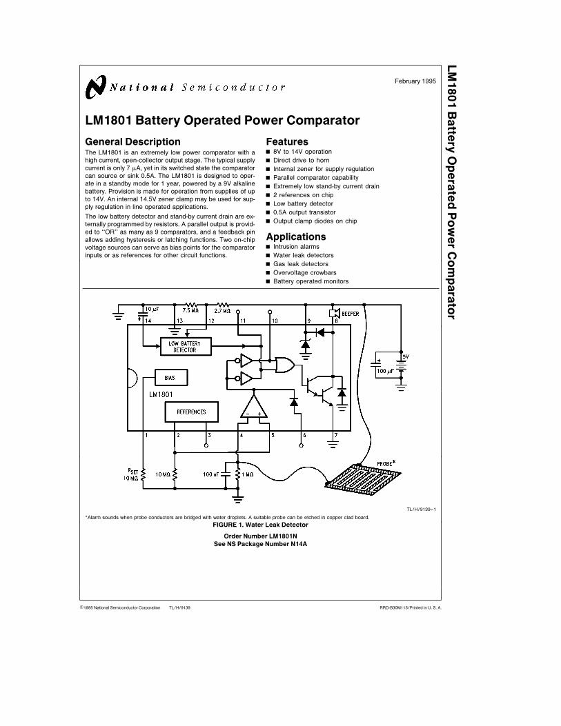
TL/H/9139–1
*Alarm sounds when probe conductors are bridged with water droplets. A suitable probe can be etched in copper clad board.
FIGURE 1. Water Leak Detector
Order Number LM1801N
See NS Package Number N14A
C1995 National Semiconductor Corporation RRD-B30M115/Printed in U. S. A.

Absolute Maximum RatingsIf Military/Aerospace specified devices are required,
please contact the National Semiconductor Sales
Office/Distributors for availability and specifications.
Supply Voltage 14V
Input Voltage b0.3V to 14V
Input Differential Voltage g14V
Power Dissipation (Note 1) 1176 mW
Operating Temperature Range 0§C to a70§CStorage Temperature Range b65§C to a125§CLead Temperature (Soldering, 10 sec.) 260§CESD rating to be determined.
Electrical Characteristics (Note 2)
Parameter Conditions Min Typ Max Units
Comparator
Input Offset Voltage 5 15 mV
Input Bias Current 2 10 nA
Input Offset Current 0.5 8 nA
Pin 6 Output Low ISINK e 100 mA 1.5 V
Output Stage (Pin 8)
Leakage Current 5 100 nA
Saturation Voltage I8 e 200 mA 0.7 1.3 V
Saturation Voltage I8 e 500 mA 1.9 V
Common Alarm Line (Pin 10)
Drive Capabilities V4 l V5
Output Voltage High 6.8 V
Output Current V10 e 0.0V 6.5 mA
Driver Requirements V5 l V4
Input Voltage 3.6 V
Input Current V8 e 1.5V, I8 e 200 mA 0.4 mA
Regulator
Pin 2 Reference Voltage 5.8 V
Temperature Coefficient 5 mV/§CPin 3 Reference Voltage 5.2 V
Temperature Coefficient 7 mV/§CBattery Check Oscillator
Threshold Voltage (Pin 12) 5.5 6.0 6.5 V
Period Va e 7.5V, C1 e 10 mF 40 50 s
Beep Pulse Width Va e 7.5V, C1 e 10 mF 60 ms
Supply Current (Note 3) 6 8 mA
Zener Clamp Voltage, V9 I9 e 1 mA 14.5 V
Note 1: For operating at elevated temperatures, the device must be derated based on a 125§C maximum junction temperature and a thermal resistance of 85§C/W
junction to ambient.
Note 2: RSET e 10 MX, Va e 9V, TA e 25§C, (Figure 1).
Note 3: Output OFF.
2

TL/H
/9139–2
FIG
UR
E2.LM
1801
Inte
rnalSchem
atic
3

Applications HintsCIRCUIT OPERATION
The LM1801 includes a bias string, comparator, steering
logic, output transistor, supply clamp, low voltage detector,
and reference. An internal schematic is shown in Figure 2.
The chip is biased by a group of current sources that are
controlled externally by a fixed resistor, Rset. In normal, or
standby operation the supply current drain is nominally 6
times the set current at pin 1. The voltage at pin 1 is two
forward diode potentials (D1 a D2 e 1.2V typical) less than
the positive supply voltage. Practical values of Rset range
from 100 kX to 10 MX. Higher currents are useful where
speed is important, while lower currents promote long bat-
tery life.
The total standby current drain of the LM1801 will include, in
addition to the above, the current drawn by the external
circuits connected at pins 2, 3, and 12. These are the resis-
tive dividers used to set the low battery threshold and com-
parator threshold.
The voltage comparator consists of devices Q1 through
Q10. The input features a common mode range from less
than 300 mV to Va b 1.2V. If the non-inverting input is
within this range, the output state remains valid for inverting
inputs of 0V to Va. If the inverting input is within the com-
mon mode range, valid comparisons hold for non-inverting
inputs of 300 mV to Va. The comparator may not switch
low if the positive input is grounded.
With a set resistance of 10 MX, comparator input bias cur-
rents of 2 nA are typical. This allows the use of high-value
resistors (10 MX) at the comparator inputs which help mini-
mize total supply current. The comparator’s output is avail-
able through a steering diode (D3) for latching or hysteresis
functions.
The comparator output is also coupled internally to the
steering logic (Q11–Q13). The comparator, low battery de-
tector, and parallel output (pin 10) functions are OR’d in the
logic circuit. In addition, the comparator output is steered to
the parallel output. If the parallel outputs (pin 10) of two or
more chips are wired together along with a common ground,
the comparator on any one chip can cause all of the other
output stages to switch, as well as its own output. Outputs
are switched when the inverting comparator input is positive
with respect to the non-inverting input. Low battery func-
tions are coupled to the steering logic via Q12, and there-
fore do not affect the parallel output (Q13).
If the sense outputs (pin 11) of two or more chips are wired
together, the comparator and low battery detector will cause
all outputs to switch.
The output transistor is a 0.5A Darlington. Included in this
structure are two clamp diodes. D4 clamps positive collector
voltage excursions to the supply, and D5 clamps negative
excursions to ground.
The output transistor is normally operated with the emitter
grounded. Under these conditions the collector is guaran-
teed to saturate no higher than 1.3V at 200 mA. 1.9V satura-
tion voltage is typical at 500 mA. The emitter may also be
used as an output, and it can swing from ground potential up
to 5V on a 9V supply. Emitter swing in the positive direction
is limited in the parallel output mode.
A low battery detector with a 6V threshold is also included
on chip. This circuit consists of Q16, Q17, D11, and D12.
When pin 12, the battery sense input, is higher than 6V, D12
clamps the emitter of Q16 to 6.6V, and the output from the
current source flows through the zener to ground. If pin 14
drops below 6V, Q16 is biased ON, and current is drawn
away from the zener and into Q16. The SCR formed by Q16
and Q17 is triggered when Q16 is biased ON. The capacitor
at pin 14 is discharged, part of its charge flows to the steer-
ing logic to pulse the output transistor, and the remainder
holds the SCR in its ON state.
When the timing capacitor has discharged, conduction in
Q16 and Q17 is commutated. Note that the output from the
current source is less than the sustaining current required
by the SCR. The current source slowly charges the capaci-
tor until the voltage across it rises 0.6V above pin 12, where
the cycle repeats itself. If pin 12 rises above 6V, the zener
clamps the voltage at pin 14 and the low battery detector
remains OFF.
Pin 12 is biased from an external resistive divider. The divid-
er should be designed to detect at no lower than Va e 7V.
The detector will continue to work at lower voltages provid-
ing pin 12 is at least 1V below the supply. For a 9V alkaline
battery a threshold of 8.2V is common. A resistive divider of
2.7 MX and 7.5 MX provides the appropriate threshold.
In many applications the on-chip references can provide
bias points. The references are driven from D13, and buff-
ered by Q18 and Q19. If only one bias point is needed the
first reference (pin 2) should be used, and the unused out-
put (pin 3) may be left open. The tiny leakage currents in
Q18 can cause Q19 (pin 3) to drift upward if a 10 MX load
resistor is not included at pin 2. The combined output cur-
rent from pins 2 and 3 should not exceed 1 mA. If neither
reference output is used, pins 2 and 3 should be left open.
The last section of the LM1801 is the supply zener. It is built
from a series combination of two diodes and two zeners.
The breakdown voltage at 1 mA is 14.5V, and the series
resistance is about 200X. In line operated applications the
zener may be used for supply regulation or transient protec-
tion. The zener is designed to carry up to 10 mA.
4

Applications Hints (Continued)
DESIGN HINTS
If the comparator inputs are subjected to electrostatic dis-
charges (ESD), a series resistance is recommended to pro-
vide protection. Given the low input bias currents, 100 kXresistors can be added without affecting circuit perform-
ance, yet they greatly enhance static protection. The
LM1801 is not designed to withstand reverse battery.
With a 10 MX Rset, the LM1801 responds to an input in
approximately 2.5 ms, and turns OFF in 200 ms. Higher set
currents decrease the response time. With Rset e 1 MX,
the output switches low in 0.5 ms, and high in 50 ms, and
with Rset e 100 kX, the response times are reduced to
0.2 ms and 12 ms.
When the circuit is in the standby state (V5 l V4), the cur-
rent consumption in a typical application such as Figure 1 is
less than approximately 7 mA. However, when the compara-
tor switches LOW (V4 l V5), the supply current increases
to 3 mA owing to the Darlington base current. Therefore, to
realize maximum battery life, any application should be de-
vised so that V5 l V4 in the standby or resting state.
The output stage can drive lamps, LEDs, buzzers, beepers,
relays, motors, and solenoids. However, the low battery de-
tector is not compatible with every load. Since the low bat-
tery detector generates only a short pulse (60 ms typical), it
is intended for use with buzzers and beepers. Depending on
the response time and resonant frequency, some buzzers
may only produce a single click. Self-oscillating beepers
usually start instantly and produce a recognizable ‘‘tweet’’
when a low battery condition is detected. Incandescent
lamps, large relays and solenoids will do absolutely nothing
when pulsed by the low battery detector.
Self-oscillating beepers are readily available, such as the
Sonalert SNP428 and the Panasonic EAL-069A. These
units are guaranteed to self-start when power is applied.
To defeat the low battery detector, short pins 12 and 14
together, and do not connect them to anything else.
Circuit board assembly procedures should include a thor-
ough cleaning to remove flux and other residues. The input
pins are often biased by very high impedance sources and
even a 10 MX leakage path can upset circuit operation.
TL/H/9139–3
R1 a R2 e 10 MX
VTRIP e #R1 a R2
R2 J 5.8V
Minimum trip voltage e 5.8V
*Use series resistor for supplies l 14V. Select for IZENER e 5 mA.
**Reverse connections and add 1 MX resistor for overvoltage indication.
²Optional filter capacitor, 1 nF to 100 nF.
²²Push to reset. Eliminate pin 6 connection for non-latching operation.
FIGURE 3. Under (Over) Voltage Indicator
5

Applications Hints (Continued)
TL/H/9139–4
R1 a R2 e 10 MX
VTRIP e #R1 a R2
R2 J 5.8V
*Use series resistor for supplies l 14V.
²Optional filter capacitor, 1 nF to 100 nF.
FIGURE 4. Overvoltage Crowbar
6

Applications Hints (Continued)
TL/H/9139–5
To set trip point, trim VREF to 4.5V. Trim RSENSOR at room temperature (23§C) for:
VSENSOR e 4.5 # 273 a 23
TX a 273 Jwhere TX is the desired trip point temperature in §C. As shown, the alarm is activated for over temperature conditions. Reverse the comparator connections for
under temperature alarm. The 20 kX potentiometer allows an adjustment range of b55§C to a60§C. Add a 10k fixed resistance in series with the potentiometer for
a a50§C to a125§C adjustment range. RSENSOR can be replaced by a fixed resistor once the desired value is found. VREF is used as a final adjustment.
FIGURE 5. Over (Under) Temperature Alarm
7

Applications Hints (Continued)
TL/H/9139–6
FIGURE 6. Simple Alarm Circuit
TL/H/9139–7
FIGURE 7. Full-Featured Intrusion Alarm
8

9
LM
1801
Batt
ery
Opera
ted
Pow
erC
om
para
tor
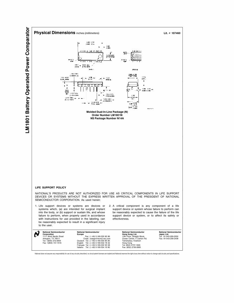
Physical Dimensions inches (millimeters) Lit. Ý 107460
Molded Dual-In-Line Package (N)
Order Number LM1801N
NS Package Number N14A
LIFE SUPPORT POLICY
NATIONAL’S PRODUCTS ARE NOT AUTHORIZED FOR USE AS CRITICAL COMPONENTS IN LIFE SUPPORT
DEVICES OR SYSTEMS WITHOUT THE EXPRESS WRITTEN APPROVAL OF THE PRESIDENT OF NATIONAL
SEMICONDUCTOR CORPORATION. As used herein:
1. Life support devices or systems are devices or 2. A critical component is any component of a life
systems which, (a) are intended for surgical implant support device or system whose failure to perform can
into the body, or (b) support or sustain life, and whose be reasonably expected to cause the failure of the life
failure to perform, when properly used in accordance support device or system, or to affect its safety or
with instructions for use provided in the labeling, can effectiveness.
be reasonably expected to result in a significant injury
to the user.
National Semiconductor National Semiconductor National Semiconductor National SemiconductorCorporation Europe Hong Kong Ltd. Japan Ltd.1111 West Bardin Road Fax: (a49) 0-180-530 85 86 13th Floor, Straight Block, Tel: 81-043-299-2309Arlington, TX 76017 Email: cnjwge@ tevm2.nsc.com Ocean Centre, 5 Canton Rd. Fax: 81-043-299-2408Tel: 1(800) 272-9959 Deutsch Tel: (a49) 0-180-530 85 85 Tsimshatsui, KowloonFax: 1(800) 737-7018 English Tel: (a49) 0-180-532 78 32 Hong Kong
Fran3ais Tel: (a49) 0-180-532 93 58 Tel: (852) 2737-1600Italiano Tel: (a49) 0-180-534 16 80 Fax: (852) 2736-9960
National does not assume any responsibility for use of any circuitry described, no circuit patent licenses are implied and National reserves the right at any time without notice to change said circuitry and specifications.


