Embed Size (px)
Citation preview

LM231,LM331
LM231A/LM231/LM331A/LM331 Precision Voltage-to-Frequency Converters
Literature Number: SNOSBI2A
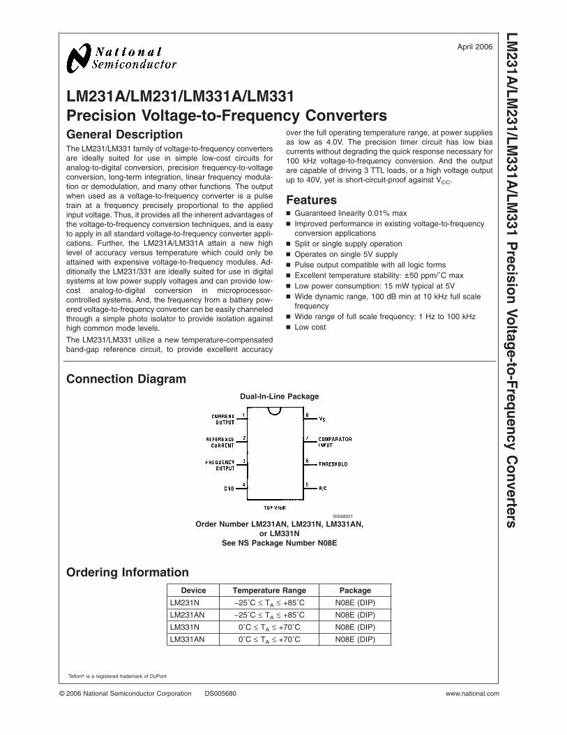
LM231A/LM231/LM331A/LM331Precision Voltage-to-Frequency ConvertersGeneral DescriptionThe LM231/LM331 family of voltage-to-frequency convertersare ideally suited for use in simple low-cost circuits foranalog-to-digital conversion, precision frequency-to-voltageconversion, long-term integration, linear frequency modula-tion or demodulation, and many other functions. The outputwhen used as a voltage-to-frequency converter is a pulsetrain at a frequency precisely proportional to the appliedinput voltage. Thus, it provides all the inherent advantages ofthe voltage-to-frequency conversion techniques, and is easyto apply in all standard voltage-to-frequency converter appli-cations. Further, the LM231A/LM331A attain a new highlevel of accuracy versus temperature which could only beattained with expensive voltage-to-frequency modules. Ad-ditionally the LM231/331 are ideally suited for use in digitalsystems at low power supply voltages and can provide low-cost analog-to-digital conversion in microprocessor-controlled systems. And, the frequency from a battery pow-ered voltage-to-frequency converter can be easily channeledthrough a simple photo isolator to provide isolation againsthigh common mode levels.
The LM231/LM331 utilize a new temperature-compensatedband-gap reference circuit, to provide excellent accuracy
over the full operating temperature range, at power suppliesas low as 4.0V. The precision timer circuit has low biascurrents without degrading the quick response necessary for100 kHz voltage-to-frequency conversion. And the outputare capable of driving 3 TTL loads, or a high voltage outputup to 40V, yet is short-circuit-proof against VCC.
Featuresn Guaranteed linearity 0.01% maxn Improved performance in existing voltage-to-frequency
conversion applicationsn Split or single supply operationn Operates on single 5V supplyn Pulse output compatible with all logic formsn Excellent temperature stability: ±50 ppm/˚C maxn Low power consumption: 15 mW typical at 5Vn Wide dynamic range, 100 dB min at 10 kHz full scale
frequencyn Wide range of full scale frequency: 1 Hz to 100 kHzn Low cost
Connection DiagramDual-In-Line Package
00568021
Order Number LM231AN, LM231N, LM331AN,or LM331N
See NS Package Number N08E
Ordering InformationDevice Temperature Range Package
LM231N −25˚C ≤ TA ≤ +85˚C N08E (DIP)
LM231AN −25˚C ≤ TA ≤ +85˚C N08E (DIP)
LM331N 0˚C ≤ TA ≤ +70˚C N08E (DIP)
LM331AN 0˚C ≤ TA ≤ +70˚C N08E (DIP)
Teflon® is a registered trademark of DuPont
April 2006LM
231A/LM
231/LM331A
/LM331
Precision
Voltage-to-FrequencyC
onverters
© 2006 National Semiconductor Corporation DS005680 www.national.com
Absolute Maximum Ratings(Notes 1, 2)
If Military/Aerospace specified devices are required,please contact the National Semiconductor Sales Office/Distributors for availability and specifications.
Supply Voltage, VS 40V
Output Short Circuit to Ground Continuous
Output Short Circuit to VCC Continuous
Input Voltage −0.2V to +VS
Package Dissipation at 25˚C 1.25W (Note 3)
Lead Temperature (Soldering, 10 sec.)
Dual-In-Line Package (Plastic) 260˚C
ESD Susceptibility (Note 5) 500V
Operating Ratings (Note 2)
Operating Ambient Temperature
LM231, LM231A −25˚C to +85˚C
LM331, LM331A 0˚C to +70˚C
Supply Voltage, VS +4V to +40V
Package Thermal ResistancePackage θJ-A
8-Lead Plastic DIP 100˚C/W
Electrical CharacteristicsAll specifications apply in the circuit of Figure 4, with 4.0V ≤ VS ≤ 40V, TA=25˚C, unless otherwise specified.
Parameter Conditions Min Typ Max Units
VFC Non-Linearity (Note 4)4.5V ≤ VS ≤ 20V ±0.003 ±0.01 % Full- Scale
TMIN ≤ TA ≤ TMAX ±0.006 ±0.02 % Full- Scale
VFC Non-Linearity in Circuit of Figure 3 VS = 15V, f = 10 Hz to 11 kHz ±0.024 ±0.14 %Full- Scale
Conversion Accuracy Scale Factor (Gain)
LM231, LM231A VIN = −10V, RS = 14 kΩ 0.95 1.00 1.05 kHz/V
LM331, LM331A 0.90 1.00 1.10 kHz/V
Temperature Stability of Gain
LM231/LM331 TMIN ≤ TA ≤ TMAX, 4.5V ≤ VS ≤ 20V ±30 ±150 ppm/˚C
LM231A/LM331A ±20 ±50 ppm/˚C
Change of Gain with VS
4.5V ≤ VS ≤ 10V 0.01 0.1 %/V
10V ≤ VS ≤ 40V 0.006 0.06 %/V
Rated Full-Scale Frequency VIN = −10V 10.0 kHz
Gain Stability vs. Time (1000 Hours) TMIN ≤ TA ≤ TMAX ±0.02 % Full- Scale
Over Range (Beyond Full-Scale)Frequency
VIN = −11V 10 %
INPUT COMPARATOR
Offset Voltage ±3 ±10 mV
LM231/LM331 TMIN ≤ TA ≤ TMAX ±4 ±14 mV
LM231A/LM331A TMIN ≤ TA ≤ TMAX ±3 ±10 mV
Bias Current −80 −300 nA
Offset Current ±8 ±100 nA
Common-Mode Range TMIN ≤ TA ≤ TMAX −0.2 VCC−2.0 V
TIMER
Timer Threshold Voltage, Pin 5 0.63 0.667 0.70 x VS
Input Bias Current, Pin 5 VS = 15V
All Devices 0V ≤ VPIN 5 ≤ 9.9V ±10 ±100 nA
LM231/LM331 VPIN 5 = 10V 200 1000 nA
LM231A/LM331A VPIN 5 = 10V 200 500 nA
VSAT PIN 5 (Reset) I = 5 mA 0.22 0.5 V
CURRENT SOURCE (Pin 1)
Output Current
LM231, LM231A RS = 14 kΩ, VPIN 1 = 0 126 135 144 µA
LM331, LM331A 116 136 156 µA
Change with Voltage 0V ≤ VPIN 1 ≤ 10V 0.2 1.0 µA
Current Source OFF Leakage
LM23
1A/L
M23
1/LM
331A
/LM
331
www.national.com 2

Electrical Characteristics (Continued)All specifications apply in the circuit of Figure 4, with 4.0V ≤ VS ≤ 40V, TA=25˚C, unless otherwise specified.
Parameter Conditions Min Typ Max Units
CURRENT SOURCE (Pin 1)
LM231, LM231A, LM331, LM331A 0.02 10.0 nA
All Devices TA = TMAX 2.0 50.0 nA
Operating Range of Current (Typical) (10 to 500) µA
REFERENCE VOLTAGE (Pin 2)
LM231, LM231A 1.76 1.89 2.02 VDC
LM331, LM331A 1.70 1.89 2.08 VDC
Stability vs. Temperature ±60 ppm/˚C
Stability vs. Time, 1000 Hours ±0.1 %
LOGIC OUTPUT (Pin 3)
VSAT
I = 5 mA 0.15 0.50 V
I = 3.2 mA (2 TTL Loads),TMIN ≤ TA ≤ TMAX
0.10 0.40 V
OFF Leakage ±0.05 1.0 µA
SUPPLY CURRENT
LM231, LM231AVS = 5V 2.0 3.0 4.0 mA
VS = 40V 2.5 4.0 6.0 mA
LM331, LM331AVS = 5V 1.5 3.0 6.0 mA
VS = 40V 2.0 4.0 8.0 mA
Note 1: Absolute Maximum Ratings indicate limits beyond which damage to the device may occur. DC and AC electrical specifications do not apply when operatingthe device beyond its specified operating conditions.
Note 2: All voltages are measured with respect to GND = 0V, unless otherwise noted.
Note 3: The absolute maximum junction temperature (TJmax) for this device is 150˚C. The maximum allowable power dissipation is dictated by TJmax, thejunction-to-ambient thermal resistance (θJA), and the ambient temperature TA, and can be calculated using the formula PDmax = (TJmax - TA) / θJA. The values formaximum power dissipation will be reached only when the device is operated in a severe fault condition (e.g., when input or output pins are driven beyond the powersupply voltages, or the power supply polarity is reversed). Obviously, such conditions should always be avoided.
Note 4: Nonlinearity is defined as the deviation of fOUT from VIN x (10 kHz/−10 VDC) when the circuit has been trimmed for zero error at 10 Hz and at 10 kHz, overthe frequency range 1 Hz to 11 kHz. For the timing capacitor, CT, use NPO ceramic, Teflon®, or polystyrene.
Note 5: Human body model, 100 pF discharged through a 1.5 kΩ resistor.
LM231A
/LM231/LM
331A/LM
331
www.national.com3
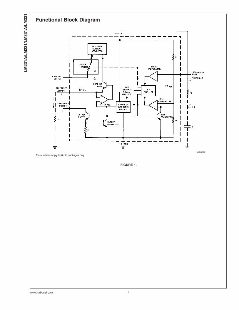
Functional Block Diagram
00568002
Pin numbers apply to 8-pin packages only.
FIGURE 1.
LM23
1A/L
M23
1/LM
331A
/LM
331
www.national.com 4
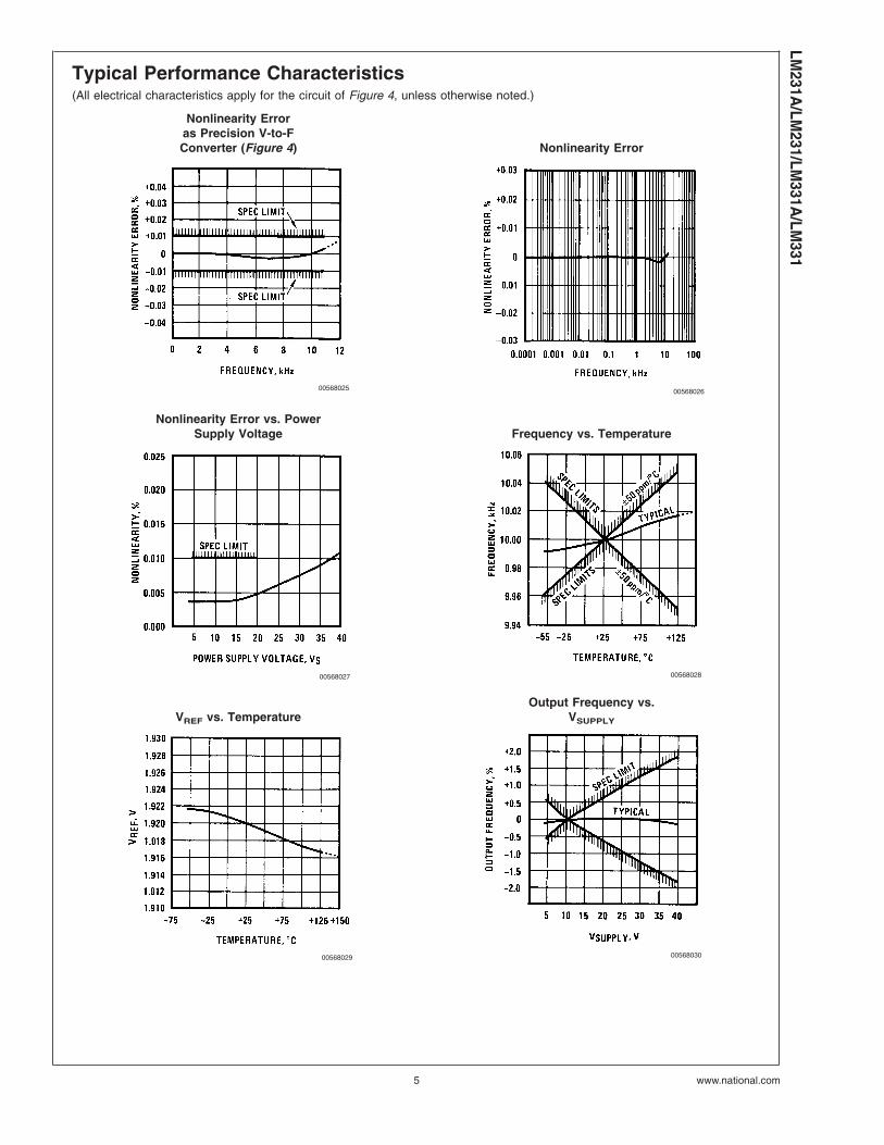
Typical Performance Characteristics(All electrical characteristics apply for the circuit of Figure 4, unless otherwise noted.)
Nonlinearity Erroras Precision V-to-FConverter (Figure 4) Nonlinearity Error
00568025 00568026
Nonlinearity Error vs. PowerSupply Voltage Frequency vs. Temperature
00568027 00568028
VREF vs. TemperatureOutput Frequency vs.
VSUPPLY
00568029 00568030
LM231A
/LM231/LM
331A/LM
331
www.national.com5
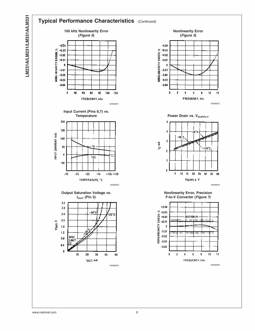
Typical Performance Characteristics (Continued)
100 kHz Nonlinearity Error(Figure 5)
Nonlinearity Error(Figure 3)
00568031 00568032
Input Current (Pins 6,7) vs.Temperature Power Drain vs. VSUPPLY
00568033 00568034
Output Saturation Voltage vs.IOUT (Pin 3)
Nonlinearity Error, PrecisionF-to-V Converter (Figure 7)
00568035 00568036
LM23
1A/L
M23
1/LM
331A
/LM
331
www.national.com 6
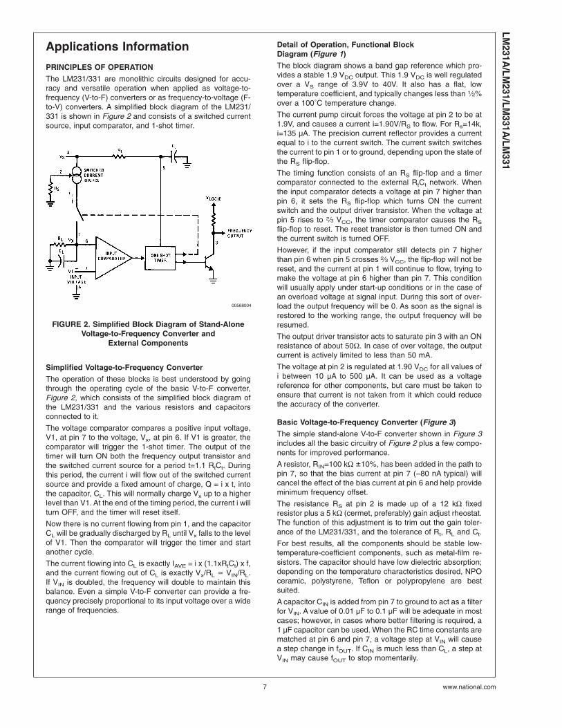
Applications Information
PRINCIPLES OF OPERATION
The LM231/331 are monolithic circuits designed for accu-racy and versatile operation when applied as voltage-to-frequency (V-to-F) converters or as frequency-to-voltage (F-to-V) converters. A simplified block diagram of the LM231/331 is shown in Figure 2 and consists of a switched currentsource, input comparator, and 1-shot timer.
Simplified Voltage-to-Frequency Converter
The operation of these blocks is best understood by goingthrough the operating cycle of the basic V-to-F converter,Figure 2, which consists of the simplified block diagram ofthe LM231/331 and the various resistors and capacitorsconnected to it.
The voltage comparator compares a positive input voltage,V1, at pin 7 to the voltage, Vx, at pin 6. If V1 is greater, thecomparator will trigger the 1-shot timer. The output of thetimer will turn ON both the frequency output transistor andthe switched current source for a period t=1.1 RtCt. Duringthis period, the current i will flow out of the switched currentsource and provide a fixed amount of charge, Q = i x t, intothe capacitor, CL. This will normally charge Vx up to a higherlevel than V1. At the end of the timing period, the current i willturn OFF, and the timer will reset itself.
Now there is no current flowing from pin 1, and the capacitorCL will be gradually discharged by RL until Vx falls to the levelof V1. Then the comparator will trigger the timer and startanother cycle.
The current flowing into CL is exactly IAVE = i x (1.1xRtCt) x f,and the current flowing out of CL is exactly Vx/RL . VIN/RL.If VIN is doubled, the frequency will double to maintain thisbalance. Even a simple V-to-F converter can provide a fre-quency precisely proportional to its input voltage over a widerange of frequencies.
Detail of Operation, Functional BlockDiagram (Figure 1)
The block diagram shows a band gap reference which pro-vides a stable 1.9 VDC output. This 1.9 VDC is well regulatedover a VS range of 3.9V to 40V. It also has a flat, lowtemperature coefficient, and typically changes less than 1⁄2%over a 100˚C temperature change.
The current pump circuit forces the voltage at pin 2 to be at1.9V, and causes a current i=1.90V/RS to flow. For Rs=14k,i=135 µA. The precision current reflector provides a currentequal to i to the current switch. The current switch switchesthe current to pin 1 or to ground, depending upon the state ofthe RS flip-flop.
The timing function consists of an RS flip-flop and a timercomparator connected to the external RtCt network. Whenthe input comparator detects a voltage at pin 7 higher thanpin 6, it sets the RS flip-flop which turns ON the currentswitch and the output driver transistor. When the voltage atpin 5 rises to 2⁄3 VCC, the timer comparator causes the RS
flip-flop to reset. The reset transistor is then turned ON andthe current switch is turned OFF.
However, if the input comparator still detects pin 7 higherthan pin 6 when pin 5 crosses 2⁄3 VCC, the flip-flop will not bereset, and the current at pin 1 will continue to flow, trying tomake the voltage at pin 6 higher than pin 7. This conditionwill usually apply under start-up conditions or in the case ofan overload voltage at signal input. During this sort of over-load the output frequency will be 0. As soon as the signal isrestored to the working range, the output frequency will beresumed.
The output driver transistor acts to saturate pin 3 with an ONresistance of about 50Ω. In case of over voltage, the outputcurrent is actively limited to less than 50 mA.
The voltage at pin 2 is regulated at 1.90 VDC for all values ofi between 10 µA to 500 µA. It can be used as a voltagereference for other components, but care must be taken toensure that current is not taken from it which could reducethe accuracy of the converter.
Basic Voltage-to-Frequency Converter (Figure 3)
The simple stand-alone V-to-F converter shown in Figure 3includes all the basic circuitry of Figure 2 plus a few compo-nents for improved performance.
A resistor, RIN=100 kΩ ±10%, has been added in the path topin 7, so that the bias current at pin 7 (−80 nA typical) willcancel the effect of the bias current at pin 6 and help provideminimum frequency offset.
The resistance RS at pin 2 is made up of a 12 kΩ fixedresistor plus a 5 kΩ (cermet, preferably) gain adjust rheostat.The function of this adjustment is to trim out the gain toler-ance of the LM231/331, and the tolerance of Rt, RL and Ct.
For best results, all the components should be stable low-temperature-coefficient components, such as metal-film re-sistors. The capacitor should have low dielectric absorption;depending on the temperature characteristics desired, NPOceramic, polystyrene, Teflon or polypropylene are bestsuited.
A capacitor CIN is added from pin 7 to ground to act as a filterfor VIN. A value of 0.01 µF to 0.1 µF will be adequate in mostcases; however, in cases where better filtering is required, a1 µF capacitor can be used. When the RC time constants arematched at pin 6 and pin 7, a voltage step at VIN will causea step change in fOUT. If CIN is much less than CL, a step atVIN may cause fOUT to stop momentarily.
00568004
FIGURE 2. Simplified Block Diagram of Stand-AloneVoltage-to-Frequency Converter and
External Components
LM231A
/LM231/LM
331A/LM
331
www.national.com7
Applications Information (Continued)
A 47Ω resistor, in series with the 1 µF CL, provides hyster-esis, which helps the input comparator provide the excellentlinearity.
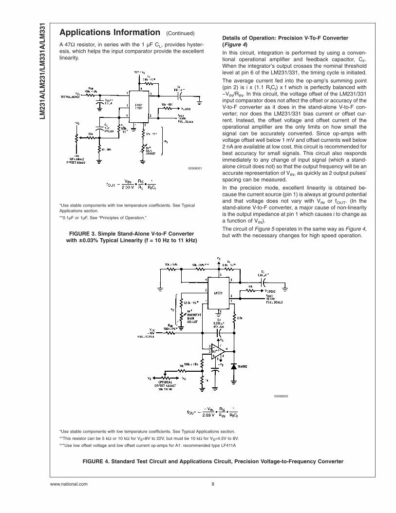
Details of Operation: Precision V-To-F Converter(Figure 4)
In this circuit, integration is performed by using a conven-tional operational amplifier and feedback capacitor, CF.When the integrator’s output crosses the nominal thresholdlevel at pin 6 of the LM231/331, the timing cycle is initiated.
The average current fed into the op-amp’s summing point(pin 2) is i x (1.1 RtCt) x f which is perfectly balanced with−VIN/RIN. In this circuit, the voltage offset of the LM231/331input comparator does not affect the offset or accuracy of theV-to-F converter as it does in the stand-alone V-to-F con-verter; nor does the LM231/331 bias current or offset cur-rent. Instead, the offset voltage and offset current of theoperational amplifier are the only limits on how small thesignal can be accurately converted. Since op-amps withvoltage offset well below 1 mV and offset currents well below2 nA are available at low cost, this circuit is recommended forbest accuracy for small signals. This circuit also respondsimmediately to any change of input signal (which a stand-alone circuit does not) so that the output frequency will be anaccurate representation of VIN, as quickly as 2 output pulses’spacing can be measured.
In the precision mode, excellent linearity is obtained be-cause the current source (pin 1) is always at ground potentialand that voltage does not vary with VIN or fOUT. (In thestand-alone V-to-F converter, a major cause of non-linearityis the output impedance at pin 1 which causes i to change asa function of VIN).
The circuit of Figure 5 operates in the same way as Figure 4,but with the necessary changes for high speed operation.
00568001
*Use stable components with low temperature coefficients. See TypicalApplications section.
**0.1µF or 1µF, See “Principles of Operation.”
FIGURE 3. Simple Stand-Alone V-to-F Converterwith ±0.03% Typical Linearity (f = 10 Hz to 11 kHz)
00568005
*Use stable components with low temperature coefficients. See Typical Applications section.
**This resistor can be 5 kΩ or 10 kΩ for VS=8V to 22V, but must be 10 kΩ for VS=4.5V to 8V.
***Use low offset voltage and low offset current op-amps for A1: recommended type LF411A
FIGURE 4. Standard Test Circuit and Applications Circuit, Precision Voltage-to-Frequency Converter
LM23
1A/L
M23
1/LM
331A
/LM
331
www.national.com 8

Applications Information (Continued)
DETAILS OF OPERATION: F-to-V CONVERTERS(Figure 6 and Figure 7)
In these applications, a pulse input at fIN is differentiated bya C-R network and the negative-going edge at pin 6 causesthe input comparator to trigger the timer circuit. Just as witha V-to-F converter, the average current flowing out of pin 1 isIAVERAGE = i x (1.1 RtCt) x f.
In the simple circuit of Figure 6, this current is filtered in thenetwork RL = 100 kΩ and 1 µF. The ripple will be less than 10mV peak, but the response will be slow, with a 0.1 secondtime constant, and settling of 0.7 second to 0.1% accuracy.
In the precision circuit, an operational amplifier provides abuffered output and also acts as a 2-pole filter. The ripple willbe less than 5 mV peak for all frequencies above 1 kHz, andthe response time will be much quicker than in Figure 6.However, for input frequencies below 200 Hz, this circuit willhave worse ripple than Figure 6. The engineering of the filtertime-constants to get adequate response and small enoughripple simply requires a study of the compromises to bemade. Inherently, V-to-F converter response can be fast, butF-to-V response can not.
00568006
*Use stable components with low temperature coefficients.
See Typical Applications section.
**This resistor can be 5 kΩ or 10 kΩ for VS=8V to 22V, but must be 10 kΩ for VS=4.5V to 8V.
***Use low offset voltage and low offset current op-amps for A1: recommended types LF411A or LF356.
FIGURE 5. Precision Voltage-to-Frequency Converter,100 kHz Full-Scale, ±0.03% Non-Linearity
LM231A
/LM231/LM
331A/LM
331
www.national.com9

Applications Information (Continued)
00568007
*Use stable components with low temperature coefficients.
FIGURE 6. Simple Frequency-to-Voltage Converter,10 kHz Full-Scale, ±0.06% Non-Linearity
00568008
*Use stable components with low temperature coefficients.
FIGURE 7. Precision Frequency-to-Voltage Converter,10 kHz Full-Scale with 2-Pole Filter, ±0.01%
Non-Linearity Maximum
LM23
1A/L
M23
1/LM
331A
/LM
331
www.national.com 10
Applications Information (Continued)
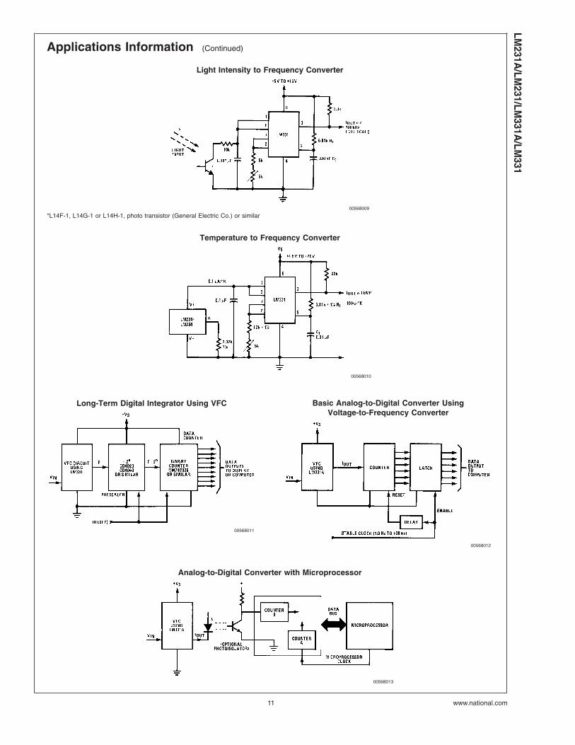
Light Intensity to Frequency Converter
00568009
*L14F-1, L14G-1 or L14H-1, photo transistor (General Electric Co.) or similar
Temperature to Frequency Converter
00568010
Long-Term Digital Integrator Using VFC
00568011
Basic Analog-to-Digital Converter UsingVoltage-to-Frequency Converter
00568012
Analog-to-Digital Converter with Microprocessor
00568013
LM231A
/LM231/LM
331A/LM
331
www.national.com11

Applications Information (Continued)
Remote Voltage-to-Frequency Converter with 2-Wire Transmitter and Receiver
00568014
Voltage-to-Frequency Converter with Square-Wave Output Using ÷ 2 Flip-Flop
00568015
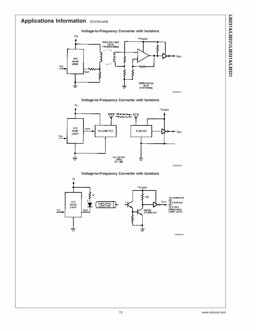
Voltage-to-Frequency Converter with Isolators
00568016
LM23
1A/L
M23
1/LM
331A
/LM
331
www.national.com 12
Applications Information (Continued)
Voltage-to-Frequency Converter with Isolators
00568017
Voltage-to-Frequency Converter with Isolators
00568018
Voltage-to-Frequency Converter with Isolators
00568019
LM231A
/LM231/LM
331A/LM
331
www.national.com13
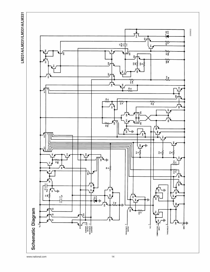
Sch
emat
icD
iag
ram
0056
8022
LM23
1A/L
M23
1/LM
331A
/LM
331
www.national.com 14
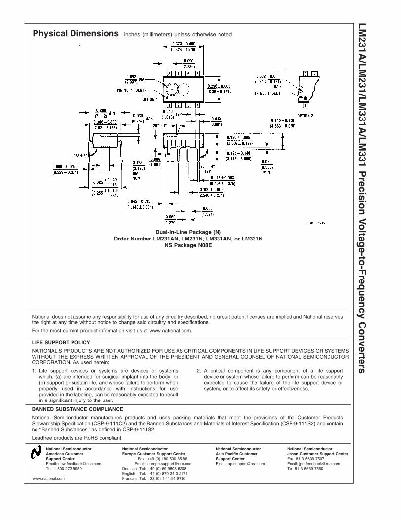
Physical Dimensions inches (millimeters) unless otherwise noted
Dual-In-Line Package (N)Order Number LM231AN, LM231N, LM331AN, or LM331N
NS Package N08E
National does not assume any responsibility for use of any circuitry described, no circuit patent licenses are implied and National reservesthe right at any time without notice to change said circuitry and specifications.
For the most current product information visit us at www.national.com.
LIFE SUPPORT POLICY
NATIONAL’S PRODUCTS ARE NOT AUTHORIZED FOR USE AS CRITICAL COMPONENTS IN LIFE SUPPORT DEVICES OR SYSTEMSWITHOUT THE EXPRESS WRITTEN APPROVAL OF THE PRESIDENT AND GENERAL COUNSEL OF NATIONAL SEMICONDUCTORCORPORATION. As used herein:
1. Life support devices or systems are devices or systemswhich, (a) are intended for surgical implant into the body, or(b) support or sustain life, and whose failure to perform whenproperly used in accordance with instructions for useprovided in the labeling, can be reasonably expected to resultin a significant injury to the user.
2. A critical component is any component of a life supportdevice or system whose failure to perform can be reasonablyexpected to cause the failure of the life support device orsystem, or to affect its safety or effectiveness.
BANNED SUBSTANCE COMPLIANCE
National Semiconductor manufactures products and uses packing materials that meet the provisions of the Customer ProductsStewardship Specification (CSP-9-111C2) and the Banned Substances and Materials of Interest Specification (CSP-9-111S2) and containno ‘‘Banned Substances’’ as defined in CSP-9-111S2.
Leadfree products are RoHS compliant.
National SemiconductorAmericas CustomerSupport CenterEmail: [email protected]: 1-800-272-9959
National SemiconductorEurope Customer Support Center
Fax: +49 (0) 180-530 85 86Email: [email protected]
Deutsch Tel: +49 (0) 69 9508 6208English Tel: +44 (0) 870 24 0 2171Français Tel: +33 (0) 1 41 91 8790
National SemiconductorAsia Pacific CustomerSupport CenterEmail: [email protected]
National SemiconductorJapan Customer Support CenterFax: 81-3-5639-7507Email: [email protected]: 81-3-5639-7560
www.national.com
LM231A
/LM231/LM
331A/LM
331P
recisionVoltage-to-Frequency
Converters
IMPORTANT NOTICE
Texas Instruments Incorporated and its subsidiaries (TI) reserve the right to make corrections, modifications, enhancements, improvements,and other changes to its products and services at any time and to discontinue any product or service without notice. Customers shouldobtain the latest relevant information before placing orders and should verify that such information is current and complete. All products aresold subject to TI’s terms and conditions of sale supplied at the time of order acknowledgment.
TI warrants performance of its hardware products to the specifications applicable at the time of sale in accordance with TI’s standardwarranty. Testing and other quality control techniques are used to the extent TI deems necessary to support this warranty. Except wheremandated by government requirements, testing of all parameters of each product is not necessarily performed.
TI assumes no liability for applications assistance or customer product design. Customers are responsible for their products andapplications using TI components. To minimize the risks associated with customer products and applications, customers should provideadequate design and operating safeguards.
TI does not warrant or represent that any license, either express or implied, is granted under any TI patent right, copyright, mask work right,or other TI intellectual property right relating to any combination, machine, or process in which TI products or services are used. Informationpublished by TI regarding third-party products or services does not constitute a license from TI to use such products or services or awarranty or endorsement thereof. Use of such information may require a license from a third party under the patents or other intellectualproperty of the third party, or a license from TI under the patents or other intellectual property of TI.
Reproduction of TI information in TI data books or data sheets is permissible only if reproduction is without alteration and is accompaniedby all associated warranties, conditions, limitations, and notices. Reproduction of this information with alteration is an unfair and deceptivebusiness practice. TI is not responsible or liable for such altered documentation. Information of third parties may be subject to additionalrestrictions.
Resale of TI products or services with statements different from or beyond the parameters stated by TI for that product or service voids allexpress and any implied warranties for the associated TI product or service and is an unfair and deceptive business practice. TI is notresponsible or liable for any such statements.
TI products are not authorized for use in safety-critical applications (such as life support) where a failure of the TI product would reasonablybe expected to cause severe personal injury or death, unless officers of the parties have executed an agreement specifically governingsuch use. Buyers represent that they have all necessary expertise in the safety and regulatory ramifications of their applications, andacknowledge and agree that they are solely responsible for all legal, regulatory and safety-related requirements concerning their productsand any use of TI products in such safety-critical applications, notwithstanding any applications-related information or support that may beprovided by TI. Further, Buyers must fully indemnify TI and its representatives against any damages arising out of the use of TI products insuch safety-critical applications.
TI products are neither designed nor intended for use in military/aerospace applications or environments unless the TI products arespecifically designated by TI as military-grade or "enhanced plastic." Only products designated by TI as military-grade meet militaryspecifications. Buyers acknowledge and agree that any such use of TI products which TI has not designated as military-grade is solely atthe Buyer's risk, and that they are solely responsible for compliance with all legal and regulatory requirements in connection with such use.
TI products are neither designed nor intended for use in automotive applications or environments unless the specific TI products aredesignated by TI as compliant with ISO/TS 16949 requirements. Buyers acknowledge and agree that, if they use any non-designatedproducts in automotive applications, TI will not be responsible for any failure to meet such requirements.
Following are URLs where you can obtain information on other Texas Instruments products and application solutions:
Products Applications
Audio www.ti.com/audio Communications and Telecom www.ti.com/communications
Amplifiers amplifier.ti.com Computers and Peripherals www.ti.com/computers
Data Converters dataconverter.ti.com Consumer Electronics www.ti.com/consumer-apps
DLP® Products www.dlp.com Energy and Lighting www.ti.com/energy
DSP dsp.ti.com Industrial www.ti.com/industrial
Clocks and Timers www.ti.com/clocks Medical www.ti.com/medical
Interface interface.ti.com Security www.ti.com/security
Logic logic.ti.com Space, Avionics and Defense www.ti.com/space-avionics-defense
Power Mgmt power.ti.com Transportation and Automotive www.ti.com/automotive
Microcontrollers microcontroller.ti.com Video and Imaging www.ti.com/video
RFID www.ti-rfid.com
OMAP Mobile Processors www.ti.com/omap
Wireless Connectivity www.ti.com/wirelessconnectivity
TI E2E Community Home Page e2e.ti.com
Mailing Address: Texas Instruments, Post Office Box 655303, Dallas, Texas 75265Copyright © 2011, Texas Instruments Incorporated