Embed Size (px)
Citation preview

OUT
UVLO/EN
VIN
GATE DIODE
R1FB
OVLO
SDASCL
PGD
SENSE
VDD
SMBusInterface
SMBA
CL
RETRY
VAUX
VDD VREF TIMERPWR
LM25066/I
Auxillary ADC Input(0V " 1.16V)
VOUT
COUT
10k
VIN
1 PF 1 PF RPWR
ADR2ADR1ADR0GND
RSNS
R2
R3
CTIMER
RFB1
RFB2
CIN Z1
Q2
Q1
D1
1k
Cdv/dt
Only required when using dv/dt start-up
Q3R4
D2
Only required when FET Vgs rating is < +/-20V
D3
Product
Folder
Sample &Buy
Technical
Documents
Tools &
Software
Support &Community
LM25066SNVS654J –FEBRUARY 2010–REVISED DECEMBER 2015
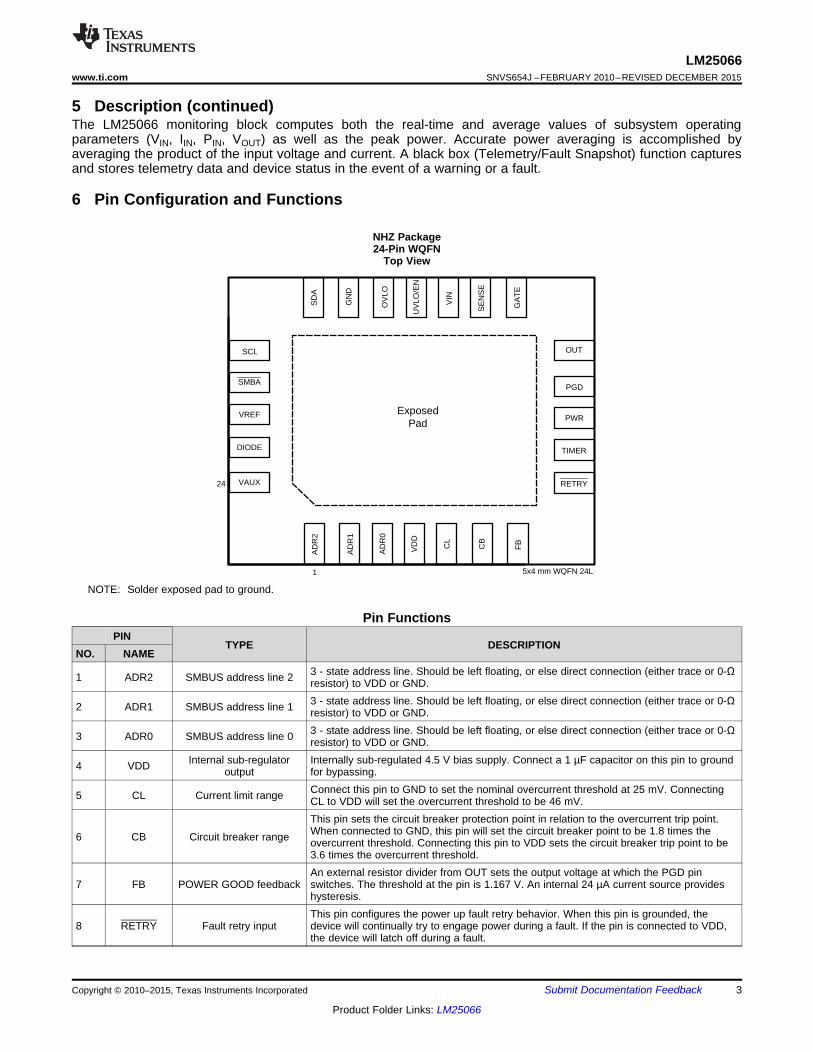
LM25066 System Power Management and Protection IC With PMBus™1 Features 2 Applications1• Input Voltage Range: 2.9 V to 17 V • Server Backplane Systems• I2C/SMBus Interface and PMBus™ Compliant • Basestation Power Distribution Systems
Command Structure • Solid-State Circuit Breaker• Programmable 25-mV or 46-mV Current Limit
3 DescriptionThresholdThe LM25066 combines a high-performance hot-• Configurable Circuit Breaker Protection for Hardswap controller with a PMBus™ compliant SMBus/I2CShortsinterface to accurately measure, protect and control• Configurable Undervoltage and Overvoltage the electrical operating conditions of computing andLockouts With Hysteresis storage blades connected to a backplane power bus.
• Remote Temperature Sensing With The LM25066 continuously supplies real-time power,Programmable Warning and Shutdown voltage, current, temperature and fault data to the
system management host via the SMBus interface.Thresholds• Detection and Notification of Damaged MOSFET The LM25066 control block includes a unique hot-
Condition swap architecture that provides current and powerlimiting to protect sensitive circuitry during insertion of• Real-Time Monitoring of VIN, VOUT, IIN, PIN, VAUXboards into a live system backplane, or any other hotWith 12-bit Resolution and 1-kHz Sampling Ratepower source. A fast acting circuit breaker prevents• Current Measurement Accuracy: ±2.4% Over damage in the event of a short circuit on the output.
Temperature The input undervoltage and overvoltage levels and• Power Measurement Accuracy: ±3% Over hysteresis are configurable, as well as the insertion
delay time and fault detection time. A temperatureTemperaturemonitoring block on the LM25066 interfaces with a• True Input Power Measurement Usinglow-cost external diode for monitoring theSimultaneous Sampling of VIN and IIN Accurately temperature of the external MOSFET or otherAverages Dynamic Power Readings thermally sensitive components. The POWER GOOD
• Averaging of VIN, IIN, PIN, and VOUT Over output provides a fast indicator when the input and/orProgrammable Interval Ranging from 0.001 to output voltages are outside their programmed range.4 Seconds LM25066 current measurement accuracy is ±2.4%
over temperature.• Programmable WARN and FAULT ThresholdsWith SMBA Notification Device Information(1)
• Blackbox Capture of Telemetry MeasurementsPART NUMBER PACKAGE BODY SIZE (NOM)and Device Status Triggered by WARN or FAULT
LN25066 WQFN (24) 5.00 mm × 4.00 mmCondition(1) For all available packages, see the orderable addendum at• Full-Featured Application Design and
the end of the data sheet.Development GUI• 24-Lead WQFN Package
Typical Application Schematic
1
An IMPORTANT NOTICE at the end of this data sheet addresses availability, warranty, changes, use in safety-critical applications,intellectual property matters and other important disclaimers. PRODUCTION DATA.

LM25066SNVS654J –FEBRUARY 2010–REVISED DECEMBER 2015 www.ti.com
Table of Contents8.3 Feature Description................................................. 161 Features .................................................................. 18.4 Device Functional Modes........................................ 182 Applications ........................................................... 18.5 Register Maps ........................................................ 223 Description ............................................................. 1
9 Application and Implementation ........................ 414 Revision History..................................................... 29.1 Application Information............................................ 415 Description (continued)......................................... 39.2 Typical Application ................................................. 416 Pin Configuration and Functions ......................... 3
10 Power Supply Recommendations ..................... 557 Specifications......................................................... 511 Layout................................................................... 557.1 Absolute Maximum Ratings ...................................... 5
11.1 Layout Guidelines ................................................. 557.2 ESD Ratings ............................................................ 511.2 Layout Example .................................................... 567.3 Recommended Operating Conditions....................... 5
12 Device and Documentation Support ................. 577.4 Thermal Information .................................................. 512.1 Device Support .................................................... 577.5 Electrical Characteristics........................................... 612.2 Community Resources.......................................... 577.6 Timing Requirements ............................................... 812.3 Trademarks ........................................................... 577.7 Switching Characteristics .......................................... 912.4 Electrostatic Discharge Caution............................ 577.8 Typical Characteristics ............................................ 1012.5 Glossary ................................................................ 578 Detailed Description ............................................ 15
13 Mechanical, Packaging, and Orderable8.1 Overview ................................................................. 15Information ........................................................... 578.2 Functional Block Diagram ....................................... 15
4 Revision HistoryNOTE: Page numbers for previous revisions may differ from page numbers in the current version.
Changes from Revision I (February 2013) to Revision J Page
• Added ESD Rating table, Feature Description section, Device Functional Modes, Application and Implementationsection, Power Supply Recommendations section, Device and Documentation Support section, and Mechanical,Packaging, and Orderable Information................................................................................................................................... 1
Changes from Revision H (February 2013) to Revision I Page
• Changed layout of National Data Sheet to TI format ........................................................................................................... 40
2 Submit Documentation Feedback Copyright © 2010–2015, Texas Instruments Incorporated
Product Folder Links: LM25066
5x4 mm WQFN 24L1
24
GA
TE
OUT
PGD
TIMER
AD
R2
AD
R1
VAUX
SCL
SMBA
VREF
DIODE
PWR
SE
NS
E
VIN
UV
LO/E
N
OV
LO
GN
D
AD
R0
SD
A
VD
D
FB
RETRY
CL
CB
ExposedPad
LM25066www.ti.com SNVS654J –FEBRUARY 2010–REVISED DECEMBER 2015
5 Description (continued)The LM25066 monitoring block computes both the real-time and average values of subsystem operatingparameters (VIN, IIN, PIN, VOUT) as well as the peak power. Accurate power averaging is accomplished byaveraging the product of the input voltage and current. A black box (Telemetry/Fault Snapshot) function capturesand stores telemetry data and device status in the event of a warning or a fault.
6 Pin Configuration and Functions
NHZ Package24-Pin WQFN
Top View
NOTE: Solder exposed pad to ground.
Pin FunctionsPIN
TYPE DESCRIPTIONNO. NAME
3 - state address line. Should be left floating, or else direct connection (either trace or 0-Ω1 ADR2 SMBUS address line 2 resistor) to VDD or GND.3 - state address line. Should be left floating, or else direct connection (either trace or 0-Ω2 ADR1 SMBUS address line 1 resistor) to VDD or GND.3 - state address line. Should be left floating, or else direct connection (either trace or 0-Ω3 ADR0 SMBUS address line 0 resistor) to VDD or GND.
Internal sub-regulator Internally sub-regulated 4.5 V bias supply. Connect a 1 µF capacitor on this pin to ground4 VDD output for bypassing.Connect this pin to GND to set the nominal overcurrent threshold at 25 mV. Connecting5 CL Current limit range CL to VDD will set the overcurrent threshold to be 46 mV.This pin sets the circuit breaker protection point in relation to the overcurrent trip point.When connected to GND, this pin will set the circuit breaker point to be 1.8 times the6 CB Circuit breaker range overcurrent threshold. Connecting this pin to VDD sets the circuit breaker trip point to be3.6 times the overcurrent threshold.An external resistor divider from OUT sets the output voltage at which the PGD pin
7 FB POWER GOOD feedback switches. The threshold at the pin is 1.167 V. An internal 24 µA current source provideshysteresis.This pin configures the power up fault retry behavior. When this pin is grounded, the
8 RETRY Fault retry input device will continually try to engage power during a fault. If the pin is connected to VDD,the device will latch off during a fault.
Copyright © 2010–2015, Texas Instruments Incorporated Submit Documentation Feedback 3
Product Folder Links: LM25066

LM25066SNVS654J –FEBRUARY 2010–REVISED DECEMBER 2015 www.ti.com
Pin Functions (continued)PIN
TYPE DESCRIPTIONNO. NAME
An external capacitor connected to this pin sets the insertion time delay, fault timeout9 TIMER Timing capacitor period and restart timing.An external resistor connected to this pin, in conjunction with the current sense resistor10 PWR Power limit set (RS), sets the maximum power dissipation allowed in the external series pass MOSFET.An open drain output. This output is high when the voltage at the FB pin is above 1.167 Vand the input supply is within its undervoltage and overvoltage thresholds. Connect via a11 PGD POWER GOOD indicator pullup resistor to the output rail (external MOSFET source) or any other voltage to bemonitored.Connect to the output rail (external MOSFET source). Internally used to determine the12 OUT Output feedback MOSFET VDS voltage for power limiting, and to monitor the output voltage.
13 GATE Gate drive output Connect to the external MOSFET's gate.The voltage across the current sense resistor (RS) is measured from VIN to this pin. If the
14 SENSE Current sense input voltage across RS reaches overcurrent threshold, the load current is limited and the faulttimer activates.A small ceramic bypass capacitor close to this pin is recommended to suppress transients15 VIN Positive supply input which occur when the load current is switched off.An external resistor divider from the system input voltage sets the undervoltage turnon
16 UVLO/EN Undervoltage lockout threshold. An internal 23-µA current source provides hysteresis. The enable threshold atthe pin is 1.16 V. This pin can also be used for remote shutdown control.An external resistor divider from the system input voltage sets the overvoltage turnoff
17 OVLO Overvoltage lockout threshold. An internal 23-µA current source provides hysteresis. The disable threshold atthe pin is 1.16 V.
18 GND Circuit ground –Data pin for SMBus. Open-drain output, requires external pullup resistor to Vdd or other19 SDA SMBus data pin voltage source.Clock pin for SMBus. Open-drain output, requires external pullup resistor to Vdd or other20 SCL SMBus clock voltage source.Alert pin for SMBus; active low. Open-drain output, requires external pullup resistor to Vdd21 SMBA SMBus alert line or other voltage source.Internally generated precision 2.73-V reference used for analog to digital conversion.22 VREF Internal reference Connect a 1-µF capacitor on this pin to ground for bypassing.Connect this to a diode-configured NPN transistor for temperature monitoring. Connect to23 DIODE External diode ground if unused.
24 VAUX Auxiliary voltage input Auxiliary pin allows voltage telemetry from an external source. Full scale input of 1.16 V.Exposed Exposed pad of WQFN No internal electrical connections. Solder to the ground plane to reduce thermal– Pad package resistance.
4 Submit Documentation Feedback Copyright © 2010–2015, Texas Instruments Incorporated
Product Folder Links: LM25066

LM25066www.ti.com SNVS654J –FEBRUARY 2010–REVISED DECEMBER 2015
7 Specifications
7.1 Absolute Maximum Ratingsover operating free-air temperature range (unless otherwise noted) (1)
MIN MAX UNITVIN, SENSE to GND (2) –0.3 24 VGATE, FB, UVLO/EN, OVLO, PGD to GND (2) –0.3 20 VOUT to GND –1 20 VInput voltageSCL, SDA, SMBA, CL, CB, ADR0, ADR1, ADR2, VDD, VAUX, –0.3 6 VDIODE, RETRY to GNDVIN to SENSE –0.3 0.3 V
Junction temperature, TJ 150 °CStorage temperature, Tstg –65 150 °C
(1) Stresses beyond those listed under Absolute Maximum Ratings may cause permanent damage to the device. These are stress ratingsonly, which do not imply functional operation of the device at these or any other conditions beyond those indicated under RecommendedOperating Conditions. Exposure to absolute-maximum-rated conditions for extended periods may affect device reliability.
(2) The GATE pin voltage is typically 7.5 V above VIN when the LM25066 is enabled. Therefore, the Absolute Maximum Rating of 24 V forVIN and SENSE apply only when the LM25066 is disabled or for a momentary surge to that voltage since the Absolute Maximum Ratingfor the GATE pin is 20 V.
7.2 ESD RatingsVALUE UNIT
Human-body model (HBM), per ANSI/ESDA/JEDEC JS-001 (1) ±2000V(ESD) Electrostatic discharge V
Charged-device model (CDM), per JEDEC specification JESD22-C101 (2) ±500
(1) JEDEC document JEP155 states that 500-V HBM allows safe manufacturing with a standard ESD control process.(2) JEDEC document JEP157 states that 250-V CDM allows safe manufacturing with a standard ESD control process.
7.3 Recommended Operating Conditionsover operating free-air temperature range (unless otherwise noted)
MIN NOM MAX UNITVIN, SENSE, OUT voltage 2.9 17 VVDD 2.9 5.5 VJunction temperature, TJ –40 125 °C
7.4 Thermal InformationLM25066
THERMAL METRIC (1) NHZ (WQFN) UNIT24 PINS
RθJA Junction-to-ambient thermal resistance 34.1 °C/WRθJC(top) Junction-to-case (top) thermal resistance 28.9 °C/WRθJB Junction-to-board thermal resistance 13.4 °C/WψJT Junction-to-top characterization parameter 0.3 °C/WψJB Junction-to-board characterization parameter 13.5 °C/WRθJC(bot) Junction-to-case (bottom) thermal resistance 3.6 °C/W
(1) For more information about traditional and new thermal metrics, see the Semiconductor and IC Package Thermal Metrics applicationreport, SPRA953.
Copyright © 2010–2015, Texas Instruments Incorporated Submit Documentation Feedback 5
Product Folder Links: LM25066

LM25066SNVS654J –FEBRUARY 2010–REVISED DECEMBER 2015 www.ti.com
7.5 Electrical CharacteristicsLimits in standard type are for TJ = 25°C only; limits in boldface type apply over the junction temperature (TJ) range of –40°Cto 85°C unless otherwise stated. Minimum and Maximum limits are guaranteed through test, design, or statistical correlation.Typical values represent the most likely parametric norm at TJ = 25°C, and are provided for reference purposes only. Unlessotherwise stated the following conditions apply: VIN = 12 V (see (1) and (2)).
PARAMETER TEST CONDITIONS MIN TYP MAX UNITINPUT (VIN PIN)IIN-EN Input current, enabled UVLO = 2 V and OVLO = 0.7 V 5.8 8 mAPOR Power on reset threshold at VIN VIN increasing 2.6 2.8 VPORHYS POREN hysteresis VIN decreasing 150 mVVDD REGULATOR (VDD PIN)
IVDD = 5 mA, VIN = 12 V 4.3 4.5 4.7 VVDD IVDD = 5 mA, VIN = 4.5 V 3.5 3.9 4.3 VVDDILIM VDD current limit 25 45 mAUVLO/EN, OVLO PINSUVLOTH UVLO threshold VUVLO Falling 1.147 1.16 1.173 VUVLOHYS UVLO hysteresis current UVLO = 1 V 18 23 28 µA
Delay to GATE high 8UVLODEL UVLO delay µs
Delay to GATE low 20UVLOBIAS UVLO bias current UVLO = 3 V 1 µAOVLOTH OVLO threshold VOVLO rising 1.141 1.16 1.185 VOVLOHYS OVLO hysteresis current OVLO = 1 V –28 –23 –18 µA
Delay to GATE high 19OVLODEL OVLO delay µs
Delay to GATE low 9OVLOBIAS OVLO bias current OVLO = 1 V 1 µAPOWER GOOD (PGD PIN)PGDVOL Output low voltage ISINK = 2 mA 25 60 mVPGDIOH Off leakage current VPGD = 17 V 1 µAPGDDELAY Power Good delay VFB to VPG 115 nsFB PINFBTH FB threshold VFB rising 1.141 1.167 1.19 VFBHYS FB hysteresis current –31 –24 –18 µAFBLEAK Off leakage current VFB = 1 V 1 µAPOWER LIMIT (PWR PIN)PWRLIM Power limit sense voltage (VIN-SENSE) SENSE-OUT = 12 V, RPWR = 25 kΩ 9 12.5 15 mVIPWR PWR pin current VPWR = 2.5 V –10 µARSAT(PWR) PWR pin impedance when disabled UVLO = 0.7 V 180 ΩGATE CONTROL (GATE PIN)
Source current Normal operation –28 –22 –16 µAFault sink current UVLO = 1 V 1.5 2 2.5 mAIGATE
VIN - SENSE = 150 mV or VIN < RPOR,POR circuit breaker sink current 105 190 275 mAVGATE = 5 VVGATE Gate output voltage in normal operation GATE voltage with respect to ground 17 18.8 20.3 VOUT PINIOUT-EN OUT bias current, enabled OUT = VIN, normal operation 16 µAIOUT-DIS OUT bias current, disabled (3) Disabled, OUT = 0 V, SENSE = VIN –12 µA
(1) Current out of a pin is indicated as a negative value.(2) All limits are specified. All electrical characteristics having room temperature limits are tested during production at TA = 25°C. All hot and
cold limits are specified by correlating the electrical characteristics to process and temperature variations and applying statistical processcontrol.
(3) OUT bias current (disabled) due to leakage current through an internal 0.9 MΩ resistance from SENSE to VOUT.
6 Submit Documentation Feedback Copyright © 2010–2015, Texas Instruments Incorporated
Product Folder Links: LM25066

LM25066www.ti.com SNVS654J –FEBRUARY 2010–REVISED DECEMBER 2015
Electrical Characteristics (continued)Limits in standard type are for TJ = 25°C only; limits in boldface type apply over the junction temperature (TJ) range of –40°Cto 85°C unless otherwise stated. Minimum and Maximum limits are guaranteed through test, design, or statistical correlation.Typical values represent the most likely parametric norm at TJ = 25°C, and are provided for reference purposes only. Unlessotherwise stated the following conditions apply: VIN = 12 V (see (1) and (2)).
PARAMETER TEST CONDITIONS MIN TYP MAX UNITCURRENT LIMIT
CL = GND 22.5 25 27VCL Threshold voltage CL = GND, TJ = 10°C to 85°C 23 25 27 mV
CL = VDD 42.3 46 49.7Enabled, SENSE = OUT 33
ISENSE SENSE input current Disabled, OUT = 0 V 46 µAEnabled, OUT = 0 V 45
CIRCUIT BREAKERThreshold voltage × 1.8 VIN - SENSE, CL = GND, CB = GND 35 45 55 mV
VCB CB:CL ratio CB = GND 1.6 1.8 2Threshold voltage × 3.6 VIN - SENSE, CL = GND, CB = VDD 70 90 110 mV
VCB CB:CL ratio CB = VDD 3.1 3.6 4TIMER (TIMER PIN)VTMRH Upper threshold 1.54 1.7 1.85 V
Restart cycles 0.85 1.0 1.07 VVTMRL Lower threshold End of 8th cycle 0.3 V
Re-enable threshold 0.3 VInsertion time current –3 –5.5 –8 µASink current, end of insertion time 1.4 1.9 2.4 mA
ITIMER Fault detection current TIMER pin = 2 V –120 –90 –60 µAFault sink current 2.8 µA
DCFAULT Fault restart duty cycle 0.67%INTERNAL REFERENCEVREF Reference voltage 2.703 2.73 2.757 VADC AND MUX
Resolution 12 BitsINL Integral non-linearity ADC only ±1 LSBTELEMETRY ACCURACY
CL = GND 30.2 mVIINFSR Current input full scale range
CL = VDD 60.4 mVCL = GND 7.32 µV
IINLSB Current input LSBCL = VDD 14.64 µV
VAUXFSR VAUX input full scale range 1.16 VVAUXLSB VAUX input LSB 283.2 µVVINFSR Input voltage full scale range 18.7 VVINLSB Input voltage LSB 4.54 mV
VIN – SENSE = 25 mV, CL = GND –2.7 2.4IINACC Input current accuracy VIN – SENSE = 25 mV, CL = GND –2.4% 2.4%TJ = 10°C to 85°C
VIN, VOUT = 12 V –1.6% 1.4%VAUX = 1 VVACC VAUX, VIN, VOUT accuracy VIN, VOUT = 12 V
VAUX = 1 V –1.4% 1.4%TJ = 10°C to 85°C
Copyright © 2010–2015, Texas Instruments Incorporated Submit Documentation Feedback 7
Product Folder Links: LM25066
LM25066SNVS654J –FEBRUARY 2010–REVISED DECEMBER 2015 www.ti.com
Electrical Characteristics (continued)Limits in standard type are for TJ = 25°C only; limits in boldface type apply over the junction temperature (TJ) range of –40°Cto 85°C unless otherwise stated. Minimum and Maximum limits are guaranteed through test, design, or statistical correlation.Typical values represent the most likely parametric norm at TJ = 25°C, and are provided for reference purposes only. Unlessotherwise stated the following conditions apply: VIN = 12 V (see (1) and (2)).
PARAMETER TEST CONDITIONS MIN TYP MAX UNITVIN = 12 V, VIN – SENSE = 25 mV,PINACC Input power accuracy –3% 3%CL = GND
REMOTE DIODE TEMPERATURE SENSORTemperature accuracy using local diode TA = 10°C to 85°C 2 10 °C
TACC Remote diode resolution 9 bitsHigh level 250 300 µA
IDIODE External diode current sourceLow level 9.4 µA
Diode current ratio 26PMBUS PIN THRESHOLDS (SMBA, SDA, SCL)VIL Data, clock input low voltage 0.8 VVIH Data, clock input high voltage 2.1 5.5 VVOL Data output low voltage IPULLUP = 500 µA 0 0.4 VILEAK Input leakage current SDA, SMBA, SCL = 5 V 1 µACONFIGURATION PIN THRESHOLDS (CB, CL, RETRY)VIH Threshold voltage 3 VILEAK Input leakage current CL, CB, RETRY = 5 V 1 mA
7.6 Timing RequirementsMIN NOM MAX UNIT
FSMB SMBus operating frequency 10 400 kHztBUF Bus free time between stop and start condition 1.3 µs
Hold time after (repeated) start condition. After this period, the first clock istHD:STA 0.6 µsgenerated.tSU:STA Repeated start condition setup time 0.6 µstSU:STO Stop condition setup time 0.6 µstHD:DAT Data hold time 300 nstSU:DAT Data setup time 100 nstTIMEOUT Clock low time-out (1) 25 35 mstLOW Clock low period 1.5 µstHIGH Clock high period (2) 0.6 µstLOW:SEXT Cumulative clock low extend time (slave device) (3) 25 mstLOW:MEXT Cumulative low extend time (master device) (4) 10 mstF Clock or data fall time (5) 20 300 nstR Clock or data rise time (5) 20 300 ns
(1) Devices participating in a transfer will timeout when any clock low exceeds the value of TTIMEOUT,MIN of 25 ms. Devices that havedetected a timeout condition must reset the communication no later than TTIMEOUT,MAX of 35 ms. The maximum value must be adheredto by both a master and a slave as it incorporates the cumulative stretch limit for both a master (10 ms) and a slave (25 ms).
(2) THIGH MAX provides a simple method for devices to detect bus idle conditions.(3) TLOW:SEXT is the cumulative time a slave device is allowed to extend the clock cycles in one message from the initial start to the stop. If
a slave exceeds this time, it is expected to release both its clock and data lines and reset itself.(4) TLOW:MEXT is the cumulative time a master device is allowed to extend its clock cycles within each byte of a message as defined from
start-to-ack, ack-to-ack, or ack-to-stop.(5) Rise and fall time are defined with TR = ( VILMAX – 0.15) to (VIHMIN + 0.15) and TF = 0.9 VDD to (VILMAX – 0.15).
8 Submit Documentation Feedback Copyright © 2010–2015, Texas Instruments Incorporated
Product Folder Links: LM25066

SCLVIH
VIL
VIH
VIL
P S S P
SDAtHD;DAT
tSU;STO
tHD;STA
tSU;STA
tSU;DAT
tHIGH
tBUF
tLOW
tR tF
LM25066www.ti.com SNVS654J –FEBRUARY 2010–REVISED DECEMBER 2015
7.7 Switching Characteristicsover operating free-air temperature range (unless otherwise noted)
PARAMETER TEST CONDITIONS MIN TYP MAX UNITCURRENT LIMITtCL Response time VIN-SENSE stepped from 0 mV to 80 mV 1.2 µsCIRCUIT BREAKER
VIN - SENSE stepped from 0 mV to 150 mV,tCB Response time 0.6 1.2 µstime to GATE low, no loadTIMER (TIMER PIN)tFAULT_DELAY Fault to GATE low delay TIMER pin reaches the upper threshold 17 µsADC AND MUXtAQUIRE Acquisition + conversion time Any channel 100 µstRR Acquisition round robin time Cycle all channels 1 ms
Figure 1. SMBus Timing Diagram
Copyright © 2010–2015, Texas Instruments Incorporated Submit Documentation Feedback 9
Product Folder Links: LM25066

-60 -40 -20 0 20 40 60 80 100120140
-18
-16
-14
-12
-10
-8
-6
-4
-2
OU
TP
UT
PIN
CU
RR
NE
T (
DIS
AB
LED
) (
A)
TEMPERATURE (°C)
VIN = 17V
VIN = 2.9V
VIN = 12V
-60 -40 -20 0 20 40 60 80 100 120 140
6
8
10
12
14
16
18
20
GA
TE
PIN
VO
LTA
GE
(V
)
TEMPERATURE (°C)
VIN = 17V
VIN = 9V
VIN = 5V
VIN = 12V
VIN = 2.9V
-40 -20 0 20 40 60 80 100 120
34
36
38
40
42
44
46
48
50
52
SE
NS
E P
IN C
UR
RE
NT
(D
ISA
BLE
D)
(A
)
TEMPERATURE (°C)
VIN = 17V
VIN = 12V
VIN = 2.9V
-60 -40 -20 0 20 40 60 80 100 120 140
4
8
12
16
20
24
28
OU
TP
UT
PIN
CU
RR
EN
T (
EN
AB
LED
) (
A)
TEMPERATURE (°C)
VIN = 17V
VIN = 12V
VIN = 2.9V
-60 -40 -20 0 20 40 60 80 10012014030
34
38
42
46
50
54
SE
NS
E P
IN C
UR
RE
NT
(E
NA
BLE
D)
(A
)
TEMPERATURE (°C)
VIN = 17V
VIN = 12V
VIN = 2.9V
-40 -20 0 20 40 60 80 100 120 140
3.0
3.5
4.0
4.5
5.0
5.5
6.0
VIN
INP
UT
CU
RR
EN
T (
mA
)
TEMPERATURE (°C)
VIN = 17V
VIN = 12V
VIN = 3V
LM25066SNVS654J –FEBRUARY 2010–REVISED DECEMBER 2015 www.ti.com
7.8 Typical CharacteristicsUnless otherwise specified the following conditions apply: TJ = 25°C, VIN = 12 V. All graphs show junction temperature.
Figure 2. VIN Pin Current Figure 3. SENSE Pin Current (Enabled)
Figure 4. SENSE Pin Current (Disabled) Figure 5. OUT Pin Current (Enabled)
Figure 6. OUT Pin Current (Disabled) Figure 7. GATE Pin Voltage
10 Submit Documentation Feedback Copyright © 2010–2015, Texas Instruments Incorporated
Product Folder Links: LM25066

-60 -40 -20 0 20 40 60 80 10012014023.0
23.2
23.4
23.6
23.8
24.0
UV
LO H
YS
TE
RE
SIS
CU
RR
EN
T (
A)
TEMPERATURE (°C)
-60 -40 -20 0 20 40 60 80 1001201401.162
1.163
1.164
1.165
1.166
1.167
1.168
1.169
1.170
1.171
1.172
FB
TH
RE
SH
OLD
(V
)
TEMPERATURE (°C)
-60 -40 -20 0 20 40 60 80 10012014018
22
26
30
34
38
42
PG
D L
OW
VO
LTA
GE
(m
V)
TEMPERATURE (°C)
PGD Sink Current = 2mA
-60 -40 -20 0 20 40 60 80 1001201401.15
1.16
1.17
UV
LO T
HR
ES
HO
LD (
V)
TEMPERATURE (°C)
VIN = 2.9 to 12V
VIN = 17V
-40 -20 0 20 40 60 80 100 120 140
0
4
8
12
16
20
24
PO
WE
R L
IMIT
TH
RE
SH
OLD
(m
V)
TEMPERATURE (°C)
RPWR=50K; CL = VDD
RPWR=25K; CL = GND
-40 -20 0 20 40 60 80 100 120 140
14
15
16
17
18
19
20
21
22
23
GA
TE
PIN
SO
UR
CE
CU
RR
EN
T (
A)
TEMPERATURE (°C)
VIN = 5V TO 17V
VIN = 2.9V
LM25066www.ti.com SNVS654J –FEBRUARY 2010–REVISED DECEMBER 2015
Typical Characteristics (continued)Unless otherwise specified the following conditions apply: TJ = 25°C, VIN = 12 V. All graphs show junction temperature.
Figure 8. GATE Pin Source Current Figure 9. Power Limit Threshold
Figure 10. PGD Low Voltage Figure 11. UVLO Threshold
Figure 12. UVLO Hysteresis Current Figure 13. FB Threshold
Copyright © 2010–2015, Texas Instruments Incorporated Submit Documentation Feedback 11
Product Folder Links: LM25066

-60 -40 -20 0 20 40 60 80 10012014040
60
80
100
120
140
160
180
200
CIR
CU
IT B
RE
AK
ER
TH
RE
SH
OLD
(m
V)
TEMPERATURE (°C)
CL = GND, CB = GND
CL = GND, CB = VDD
CL = VDD, CB = VDD
-60 -40 -20 0 20 40 60 80 100 120 140
40
41
42
43
44
45
46
47
48
49
50
CU
RR
EN
T L
IMIT
TH
RE
SH
OLD
(m
V)
TEMPERATURE (°C)
VIN = 2.9V
VIN = 5V to 17V
-60 -40 -20 0 20 40 60 80 100120140-26.0
-25.5
-25.0
-24.5
-24.0
-23.5
-23.0
FB
HY
ST
ER
ES
IS (
A)
TEMPERATURE (°C)
-60 -40 -20 0 20 40 60 80 100120140
23.0
23.5
24.0
24.5
25.0
25.5
26.0
26.5
27.0
CU
RR
EN
T L
IMIT
TH
RE
SH
OLD
(m
V)
TEMPERATURE (°C)
VIN = 2.9V
VIN = 5V to 17V
-60 -40 -20 0 20 40 60 80 100120140
1.162
1.163
1.164
1.165
1.166
1.167O
VLO
TH
RE
SH
OLD
(V
)
TEMPERATURE (°C)
VIN = 2.9V
VIN = 17V
VIN = 12V
-60 -40 -20 0 20 40 60 80 100120140
-30
-28
-26
-24
-22
-20
-18
-16
OV
LO H
YS
TE
RE
SIS
CU
RR
EN
T (
A)
TEMPERATURE (°C)
VIN = 12V to 17V
LM25066SNVS654J –FEBRUARY 2010–REVISED DECEMBER 2015 www.ti.com
Typical Characteristics (continued)Unless otherwise specified the following conditions apply: TJ = 25°C, VIN = 12 V. All graphs show junction temperature.
Figure 15. OVLO HysteresisFigure 14. OVLO Threshold
Figure 17. Current Limit ThresholdFigure 16. FB Pin Hysteresis
Figure 18. Current Limit Threshold Figure 19. Circuit Breaker Threshold (CL = VDD)
12 Submit Documentation Feedback Copyright © 2010–2015, Texas Instruments Incorporated
Product Folder Links: LM25066
40 ms/DIV
GATE
VIN
UVLO = 2.9Vhyst = 0.2V
OVLO = 15.2V
hyst = 1.2V
5V/DIV
40 ms/DIV
PGOOD
VOUT
10.7V
5V/DIV
5V/DIV
VIN
10.25V
400 ms/DIV
TIMER
VIN
GATE
VOUT
RETRY PERIOD = 1.10s
10V/DIV
10V/DIV
10V/DIV
1V/DIV
1 ms/DIV
TIMER
ILOAD
GATE
VOUT
2.5A/DIV
10V/DIV10V/DIV
1V/DIV
-60 -40 -20 0 20 40 60 80 100120140
2.70
2.71
2.72
2.73
2.74
2.75
VR
EF
(V
)
TEMPERATURE (°C)
100 ms/DIV
TIMER
VIN
GATE
VOUT
INSERTION DELAY = 140 ms
10V/DIV
10V/DIV
10V/DIV
1V/DIV
LM25066www.ti.com SNVS654J –FEBRUARY 2010–REVISED DECEMBER 2015
Typical Characteristics (continued)Unless otherwise specified the following conditions apply: TJ = 25°C, VIN = 12 V. All graphs show junction temperature.
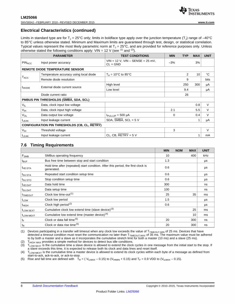
Figure 20. Reference Voltage Figure 21. Start-up (Insertion Delay)
Figure 23. Start-up (5-A Load)Figure 22. Start-up (Short Circuit VOUT)
Figure 24. Start-up (UVLO, OVLO) Figure 25. Start-up (PGOOD)
Copyright © 2010–2015, Texas Instruments Incorporated Submit Documentation Feedback 13
Product Folder Links: LM25066

-15 -5 5 15 25 35 45 55 65 75 85
-0.5
-0.4
-0.3
-0.2
-0.1
0.0
0.1
0.2
0.3
0.4
0.5
IIN E
RR
OR
( %
OF
FS
R)
TEMPERATURE ( °C)-15 -5 5 15 25 35 45 55 65 75 85
-1.0
-0.8
-0.6
-0.4
-0.2
0.0
0.2
0.4
0.6
0.8
1.0
PIN
ER
RO
R (
% O
F F
SR
)
TEMPERATURE (°C)
TIMER
ILOAD
VOUT
RETRY PERIOD = 1.1s
25A/DIV
10V/DIV
1V/DIV
400 ms/DIV
TIMER
ILOAD
GATE
VOUT
25A/DIV
10V/DIV
10V/DIV
1V/DIV
100 ms/DIV
TIMER
ILOAD
GATE
VOUT
TIMEOUT PERIOD= 8.3 ms
25A/DIV
10V/DIV
10V/DIV
1V/DIV
>50A
4 ms/DIV
TIMER
ILOAD
GATE
VOUT
50A/DIV
10V/DIV
10V/DIV
1V/DIV
> 90A TriggersCircuit Breaker
1 ms/DIV
LM25066SNVS654J –FEBRUARY 2010–REVISED DECEMBER 2015 www.ti.com
Typical Characteristics (continued)Unless otherwise specified the following conditions apply: TJ = 25°C, VIN = 12 V. All graphs show junction temperature.
Figure 26. Current Limit Event (CL = GND) Figure 27. Circuit Breaker Event (CL = CB = GND)
Figure 29. Latch Off (Retry = VDD)Figure 28. Retry Event (Retry = GND)
Figure 30. IIN Measurement Accuracy Figure 31. PIN Measurement Accuracy(VIN – SENSE = 25 mV) (VIN – SENSE = 25 mV)
14 Submit Documentation Feedback Copyright © 2010–2015, Texas Instruments Incorporated
Product Folder Links: LM25066

ID
VIN
SE
NS
E
OU
T
PW
R
GATE
22 PA
10 PA
1.16V
1.16V
OV
LO
UV
LO/E
N
23 PA
5.5 PAInsertion
Timer90 PAFault Timer
2.8 PA Fault
Discharge
1.72V
1.0V
TIMER
Current Limit Threshold
ChargePump
VDS
23 PA
TIMER AND GATE LOGIC CONTROL
GN
D
Power Limit Threshold
2 mA Gate Control 18.8V
1 M:
1.9 mA End
Insertion Time
0.3V
LM25066
Current Limit/Power Limit
Control
2.6V
VIN
POR
25 mV
190mA
1/16
S/H
1/16
VAUX
12bitADC
AM
UX
SMBUSINTERFACE
DIODE
ADR0
ADR1
ADR2
SCL
SDA
SMBA
ADDRESS DECODER
TELEMETRYSTATE
MACHINE
Gain = 2.3V/V
CL
CB
RE
TR
Y
Diode Temp Sense
Sna
pSho
t
VDD REG
VDD1.167V UV
OV
VREF
PG
D
FB
REFGEN
24 PA
MEASUREMENT/ AVERAGING
FAULT REGISTERS
2.5V
VDD
LM25066www.ti.com SNVS654J –FEBRUARY 2010–REVISED DECEMBER 2015
8 Detailed Description
8.1 OverviewThe inline protection functionality of the LM25066 is designed to control the in-rush current to the load uponinsertion of a circuit card into a live backplane or other hot power source, thereby limiting the voltage sag on thebackplane's supply voltage and the dV/dt of the voltage applied to the load. Effects on other circuits in thesystem are minimized, preventing possible unintended resets. A controlled shutdown when the circuit card isremoved can also be implemented using the LM25066.
In addition to a programmable current limit, the LM25066 monitors and limits the maximum power dissipation inthe series pass device to maintain operation within the device Safe Operating Area (SOA). Either current limitingor power limiting for an extended period of time results in the shutdown of the series pass device. In this event,the LM25066 can latch off or repetitively retry based on the hardware setting of the RETRY pin. Once started,the number of retries can be set to none, 1, 2, 4, 8, 16, or infinite. The circuit breaker function quickly switches offthe series pass device upon detection of a severe overcurrent condition. Programmable undervoltage lockout(UVLO) and overvoltage lockout (OVLO) circuits shut down the LM25066 when the system input voltage isoutside the desired operating range.
The telemetry capability of the LM25066 provides intelligent monitoring of the input voltage, output voltage, inputcurrent, input power, temperature, and an auxiliary input. The LM25066 also provides a peak capture of the inputpower and programmable hardware averaging of the input voltage, current, power, and output voltage. Warningthresholds which trigger the SMBA pin may be programmed for input and output voltage, current, power andtemperature via the PMBus interface. Additionally, the LM25066 is capable of detecting damage to the externalMOSFET, Q1.
8.2 Functional Block Diagram
Copyright © 2010–2015, Texas Instruments Incorporated Submit Documentation Feedback 15
Product Folder Links: LM25066

LM25066SNVS654J –FEBRUARY 2010–REVISED DECEMBER 2015 www.ti.com
8.3 Feature Description
8.3.1 Current LimitThe current limit threshold is reached when the voltage across the sense resistor RS (VIN to SENSE) exceedsthe internal voltage limit of 25 mV or 46 mV depending on whether the CL pin is connected to GND or VDD,respectively. In the current limiting condition, the GATE voltage is controlled to limit the current in MOSFET Q1.While the current limit circuit is active, the fault timer is active as described in Fault Timer and Restart. If the loadcurrent falls below the current limit threshold before the end of the Fault Timeout Period, the LM25066 resumesnormal operation. If the current limit condition persists for longer than the Fault Timeout Period set by the timercapacitor, CT, the IIN OC FAULT bit in the MFR_SPECIFIC_17: READ_DIAGNOSTIC_WORD (E1h) register, theINPUT bit in the STATUS_WORD (79h) register, and the IIN_OC/PFET_OP_FAULT bit in the register will betoggled high and SMBA pin will be pulled low unless this feature is disabled using the MFR_SPECIFIC_08:ALERT_MASK (D8h) register. For proper operation, the RS resistor value should be less than 200 mΩ. Highervalues may create instability in the current limit control loop. The current limit threshold pin value may beoverridden by setting appropriate bits in the MFR_SPECIFIC_09: DEVICE_SETUP (D9h).
8.3.2 Circuit BreakerIf the load current increases rapidly (for example, the load is short circuited), the current in the sense resistor(RS) may exceed the current limit threshold before the current limit control loop is able to respond. If the currentexceeds 1.8 or 3.6 times (user settable) the current limit threshold, Q1 is quickly switched off by the 190-mApulldown current at the GATE pin, and a Fault Timeout Period begins. When the voltage across RS falls belowthe threshold the 190-mA pulldown current at the GATE pin is switched off and the gate voltage of Q1 is thendetermined by the current limit or power limit functions. If the TIMER pin reaches 1.7 V before the current limitingor power limiting condition ceases, Q1 is switched off by the 2-mA pulldown current at the GATE pin as describedin Fault Timer and Restart. A circuit breaker event will cause the CIRCUIT BREAKER FAULT bit in theSTATUS_MFR_SPECIFIC (80h) and MFR_SPECIFIC_17: READ_DIAGNOSTIC_WORD (E1h) registers to betoggled high and SMBA pin will be pulled low unless this feature is disabled using the MFR_SPECIFIC_08:ALERT_MASK (D8h) register. The circuit breaker pin configuration may be overridden by setting appropriate bitsin the MFR_SPECIFIC_09: DEVICE_SETUP (D9h)) register.
8.3.3 Power LimitAn important feature of the LM25066 is the MOSFET power limiting. The Power Limit function can be used tomaintain the maximum power dissipation of MOSFET Q1 within the device SOA rating. The LM25066 determinesthe power dissipation in Q1 by monitoring its drain-source voltage (SENSE to OUT), and the drain currentthrough RS (VIN to SENSE). The product of the current and voltage is compared to the power limit thresholdprogrammed by the resistor at the PWR pin. If the power dissipation reaches the limiting threshold, the GATEvoltage is controlled to regulate the current in Q1. While the power limiting circuit is active, the fault timer is activeas described in Fault Timer and Restart. If the power limit condition persists for longer than the Fault TimeoutPeriod set by the timer capacitor, CT, the IIN_OC_FAULT bit in the STATUS_INPUT (7Ch) register, the INPUTbit in the STATUS_WORD (79h) register, and the IIN_OC/PFET_OP_FAULT bit in theMFR_SPECIFIC_17:READ_DIAGNOSTIC_WORD (E1h) register will be toggled high and SMBA pin will be pulled low unless thisfeature is disabled using the MFR_SPECIFIC_08: ALERT_MASK (D8h) register.
8.3.4 Undervoltage Lockout (UVLO)The series pass MOSFET (Q1) is enabled when the input supply voltage (VSYS) is within the operating rangedefined by the programmable undervoltage lockout (UVLO) and overvoltage lockout (OVLO) levels. Typically theUVLO level at VSYS is set with a resistor divider (R1-R3) as shown in Figure 35. Refering to the Block Diagramwhen VSYS is below the UVLO level, the internal 23-µA current source at UVLO is enabled, the current source atOVLO is off, and Q1 is held off by the 2-mA pulldown current at the GATE pin. As VSYS is increased, raising thevoltage at UVLO above its threshold the 23-µA current source at UVLO is switched off, increasing the voltage atUVLO, providing hysteresis for this threshold. With the UVLO/EN pin above its threshold, Q1 is switched on bythe 22-µA current source at the GATE pin if the insertion time delay has expired.
16 Submit Documentation Feedback Copyright © 2010–2015, Texas Instruments Incorporated
Product Folder Links: LM25066

LM25066www.ti.com SNVS654J –FEBRUARY 2010–REVISED DECEMBER 2015
Feature Description (continued)See Typical Application for a procedure to calculate the values of the threshold setting resistors (R1-R3). Theminimum possible UVLO level at VSYS can be set by connecting the UVLO/EN pin to VIN. In this case, Q1 isenabled after the insertion time when the voltage at VIN reaches the POR threshold. After power up, an UVLOcondition will toggle high the VIN UV FAULT bit in the STATUS_INPUT (7Ch), the INPUT bit in theSTATUS_WORD (79h) register, and the VIN_UNDERVOLTAGE_FAULT bit in the MFR_SPECIFIC_17:READ_DIAGNOSTIC_WORD (E1h) register, and SMBA pin will be pulled low unless this feature is disabledusing the MFR_SPECIFIC_08: ALERT_MASK (D8h) register.
8.3.5 Overvoltage Lockout (OVLO)The series pass MOSFET (Q1) is enabled when the input supply voltage (VSYS) is within the operating rangedefined by the programmable undervoltage lockout (UVLO) and overvoltage lockout (OVLO) levels. If VSYS raisesthe OVLO pin voltage above its threshold, Q1 is switched off by the 2-mA pulldown current at the GATE pin,denying power to the load. When the OVLO pin is above its threshold, the internal 23 µA current source at OVLOis switched on, raising the voltage at OVLO to provide threshold hysteresis. When VSYS is reduced below theOVLO level, Q1 is re-enabled. An OVLO condition will toggle high the VIN OV FAULT bit in the STATUS_INPUT(7Ch), the INPUT bit in the STATUS_WORD (79h) register, and the VIN_OVERVOLTAGE_FAULT bit in theMFR_SPECIFIC_17: READ_DIAGNOSTIC_WORD (E1h) register, and the SMBA pin will be pulled low unlessthis feature is disabled using the MFR_SPECIFIC_08: ALERT_MASK (D8h) register.
See Typical Application for a procedure to calculate the threshold setting resistor values.
8.3.6 Power GoodThe Power Good indicator (PGD) is connected to the drain of an internal N-channel MOSFET capable ofsustaining 17 V in the off-state, and transients up to 20 V. An external pullup resistor is required at PGD to anappropriate voltage to indicate the status to downstream circuitry. The off-state voltage at the PGD pin can behigher or lower than the voltages at VIN and OUT. PGD is switched high when the voltage at the FB pin exceedsthe PGD threshold voltage. Typically, the output voltage threshold is set with a resistor divider from output tofeedback, although the monitored voltage need not be the output voltage. Any other voltage can be monitored aslong as the voltage at the FB pin does not exceed its maximum rating. Referring to the Block Diagram, when thevoltage at the FB pin is below its threshold, the 24-µA current source at FB is disabled. As the output voltageincreases, taking FB above its threshold, the current source is enabled, sourcing current out of the pin, raisingthe voltage at FB to provide threshold hysteresis. The PGD output is forced low when either the UVLO/EN pin isbelow its threshold or the OVLO pin is above its threshold. The status of the PGD pin can be read via the PMBusinterface in either the STATUS_WORD (79h) or MFR_SPECIFIC_17: READ_DIAGNOSTIC_WORD (E1h)registers.
8.3.7 VDD Sub-RegulatorThe LM25066 contains an internal linear sub-regulator which steps down the input voltage to generate a 4.5 Vrail used for powering low voltage circuitry. When the input voltage is below 4.5 V, VDD will track VIN. For inputvoltages 3.3 V and below, VDD should be tied directly to VIN to avoid the dropout of the sub-regulator. The VDDsub-regulator should be used as the pullup supply for the CL, CB, RETRY, ADR2, ADR1, ADR0 pins if they areto be tied high. It may also be used as the pullup supply for the PGD and the SMBus signals (SDA, SCL, SMBA).The VDD sub-regulator is not designed to drive high currents and should not be loaded with other integratedcircuits. The VDD pin is current limited to 45 mA in order to protect the LM25066 in the event of a short. The sub-regulator requires a bypass capacitance having a value from 1 µF to 4.7 µF to be placed as close to the VDD pinas the PCB layout allows.
Copyright © 2010–2015, Texas Instruments Incorporated Submit Documentation Feedback 17
Product Folder Links: LM25066

LM25066SNVS654J –FEBRUARY 2010–REVISED DECEMBER 2015 www.ti.com
Feature Description (continued)8.3.8 Remote Temperature SensingThe LM25066 is designed to measure temperature remotely using an MMBT3904 NPN transistor. The base andcollector of the MMBT3904 is connected to the DIODE pin and the emitter is grounded. Place the MMBT3904near the device whose temperature is to be monitored. If the temperature of the hot-swap pass MOSFET, Q1, isto be measured, the MMBT3904 should be placed as close to Q1 as the layout allows. The temperature ismeasured by means of a change in the diode voltage in response to a step in current supplied by the DIODE pin.The DIODE pin sources a constant 9.4 µA but pulses 250 µA once every millisecond in order to measure thediode temperature. Care must be taken in the PCB layout to keep the parasitic resistance between the DIODEpin and the MMBT3904 low so as not to degrade the measurement. Additionally, a small 1000-pF bypasscapacitor should be placed in parallel with the MMBT3904 to reduce the effects of noise. The temperature can beread using the READ_TEMPERATURE_1 (8Dh) PMBus command. The default limits of the LM25066 will causeSMBA pin to be pulled low if the measured temperature exceeds 125°C and will disable the hot-swap passMOSFET if the temperature exceeds 150°C. These thresholds can be reprogrammed via the PMBus interfaceusing the OT_WARN_LIMIT (51h) and OT_FAULT_LIMIT (4Fh) commands. If the temperature measurement andprotection capability of the LM25066 is not used, the DIODE pin should be grounded.
8.3.9 Damaged MOSFET DetectionThe LM25066 is able to detect whether the external MOSFET, Q1, is damaged under certain conditions. If thevoltage across the sense resistor exceeds 4mV while the GATE voltage is low or the internal logic indicates thatthe GATE should be low, the EXT_MOSFET_SHORTED bit in the STATUS_MFR_SPECIFIC (80h) andMFR_SPECIFIC_17: READ_DIAGNOSTIC_WORD (E1h) registers will be toggled high and the SMBA pin will bepulled low unless this feature is disabled using the MFR_SPECIFIC_08: ALERT_MASK (D8h). This methodeffectively determines whether Q1 is shorted because of damage present between the drain and gate and/ordrain and source of the external MOSFET.
8.4 Device Functional Modes
8.4.1 Power Up SequenceThe VIN operating range of the LM25066 is +2.9 V to +17 V, with transient capability to +24 V. Referring toFigure 38 and Figure 32, as the voltage at VIN initially increases, the external N-channel MOSFET (Q1) is heldoff by an internal 190-mA pulldown current at the GATE pin. The strong pulldown current at the GATE pinprevents an inadvertent turnon as the MOSFET's gate-to-drain (Miller) capacitance is charged. Additionally, theTIMER pin is initially held at ground. When the VIN voltage reaches the POR threshold, the insertion time begins.During the insertion time, the capacitor at the TIMER pin (CT) is charged by a 5.5-µA current source and Q1 isheld off by a 2-mA pulldown current at the GATE pin regardless of the input voltage. The insertion time delayallows ringing and transients at VIN to settle before Q1 is enabled. The insertion time ends when the TIMER pinvoltage reaches 1.7 V. CT is then quickly discharged by an internal 1.9-mA pulldown current. The GATE pin thenswitches on Q1 when VSYS, the input supply voltage, exceeds the UVLO threshold. If VSYS is above the UVLOthreshold at the end of the insertion time, Q1 switches on at that time. The GATE pin charge pump sources 22µA to charge the gate capacitance of Q1. The maximum voltage at the GATE pin with respect to ground is limitedby an internal 18.8-V Zener diode.
As the voltage at the OUT pin increases, the LM25066 monitors the drain current and power dissipation ofMOSFET Q1. Inrush current limiting and/or power limiting circuits actively control the current delivered to theload. During the inrush limiting interval (t2 in Figure 32), an internal 90 -A fault timer current source charges CT. IfQ1's power dissipation and the input current reduce below their respective limiting thresholds before the TIMERpin reaches 1.7 V, the 90-µA current source is switched off and CT is discharged by the internal 2.8-µA currentsink (t3 in Figure 32). The PGD pin switches high when FB exceeds its rising threshold of 1.167 V.
If the TIMER pin voltage reaches 1.7 V before inrush current limiting or power limiting ceases during t2, a fault isdeclared and Q1 is turned off. See Fault Timer and Restart for a complete description of the fault mode.
The LM25066 will pull the SMBA pin low after the input voltage has exceeded its POR threshold to indicate thatthe volatile memory and device settings are in their default state. The CONFIG_PRESET bit within theSTATUS_MFR_SPECIFIC (80h) indicates default configuration of warning thresholds and device operation andwill remain set until a CLEAR_FAULTS command is received.
18 Submit Documentation Feedback Copyright © 2010–2015, Texas Instruments Incorporated
Product Folder Links: LM25066

t1 t2 t3
Normal OperationInsertion Time
22 PA source
2.8 PA90PA
ILIMIT
190 mApull-down
GATEPin
RTIMEPin
VIN
VSYS
UVLO
POR
LoadCurrent
OutputVoltage
(OUT Pin)
PGD
In rushLimiting
1.7V5.5 PA
2 mA pull-down
LM25066www.ti.com SNVS654J –FEBRUARY 2010–REVISED DECEMBER 2015
Device Functional Modes (continued)
Figure 32. Power Up Sequence (Current Limit Only)
8.4.2 Gate ControlA charge pump provides the voltage at the GATE pin to enhance the N-Channel MOSFET's gate. During normaloperating conditions (t3 in Figure 32) the gate of Q1 is held charged by an internal 22-µA current source. Thevoltage at the GATE pin (with respect to ground) is limited by an internal 18.8-V Zener diode. See the graphFigure 7 in Typical Characteristics. Since the gate-to-source voltage applied to Q1 could be as high as 18.8 Vduring various conditions, a Zener diode with the appropriate voltage rating must be added between the GATEand OUT pins if the maximum VGS rating of the selected MOSFET is less than 18.8 V. The external Zener diodemust have a forward current rating of at least 190 mA. When the system voltage is initially applied, the GATE pinis held low by a 190-mA pulldown current. This helps prevent an inadvertent turnon of the MOSFET through itsdrain-gate capacitance as the applied system voltage increases.
During the insertion time (t1 in Figure 32) the GATE pin is held low by a 2-mA pulldown current. This maintainsQ1 in the off-state until the end of t1, regardless of the voltage at VIN or UVLO. Following the insertion time (t2 inFigure 32), the gate voltage of Q1 is controlled to keep the current or power dissipation level from exceeding theprogrammed levels. While in the current or power limiting mode, the TIMER pin capacitor is charging. If thecurrent and power limiting cease before the TIMER pin reaches 1.7 V, the TIMER pin capacitor then discharges,and the circuit begins normal operation. If the inrush limiting condition persists such that the TIMER pin reached1.7 V during t2, the GATE pin is then pulled low by the 190-mA pulldown current. The GATE pin is then held lowuntil either a power up sequence is initiated (RETRY pin to VDD), or an automatic retry is attempted (RETRY pinto GROUND). See Fault Timer and Restart. If the system input voltage falls below the UVLO threshold or risesabove the OVLO threshold, the GATE pin is pulled low by the 2-mA pulldown current to switch off Q1.
Copyright © 2010–2015, Texas Instruments Incorporated Submit Documentation Feedback 19
Product Folder Links: LM25066

1V1 2 3 7 8
2 mA pulldown
90 PA
FaultDetection
GATEPin
LoadCurrent
TILIMI
PinTIMER
0.3VtRESTART
1.7V
Fault TimeoutPeriod
22 PAGate Charge
2.8PA
LM25066RestartControl
VIN
VSYS
UVLO/EN
OVLO
GND
R1
R2
R3
LM25066SNVS654J –FEBRUARY 2010–REVISED DECEMBER 2015 www.ti.com
Device Functional Modes (continued)8.4.3 Fault Timer and RestartWhen the current limit or power limit threshold is reached during turnon, or as a result of a fault condition, thegate-to-source voltage of Q1 is controlled to regulate the load current and power dissipation in Q1. When eitherlimiting function is active, a 90-µA fault timer current source charges the external capacitor (CT) at the TIMER pinas shown in Figure 32 (Fault Timeout Period). If the fault condition subsides during the Fault Timeout Periodbefore the TIMER pin reaches 1.7 V, the LM25066 returns to the normal operating mode and CT is discharged bythe 1.9-mA current sink. If the TIMER pin reaches 1.7 V during the Fault Timeout Period, Q1 is switched off by a2-mA pulldown current at the GATE pin. The subsequent restart procedure then depends on the selected retryconfiguration.
If the RETRY pin is high, the LM25066 latches the GATE pin low at the end of the Fault Timeout Period. CT isthen discharged to ground by the 2.8-µA fault current sink. The GATE pin is held low by the 2-mA pulldowncurrent until a power up sequence is externally initiated by cycling the input voltage (VSYS), or momentarily pullingthe UVLO/EN pin below its threshold with an open-collector or open-drain device as shown in Figure 33. Thevoltage at the TIMER pin must be <0.3 V for the restart procedure to be effective. The TIMER_LATCHED_OFFbit in the MFR_SPECIFIC_17: READ_DIAGNOSTIC_WORD (E1h) register will remain high while the latched offcondition persists.
Figure 33. Latched Fault Restart Control
The LM25066 provides an automatic restart sequence which consists of the TIMER pin cycling between 1.7 Vand 1 V seven times after the Fault Timeout Period, as shown in Figure 34. The period of each cycle isdetermined by the 90-µA charging current, and the 2.8-µA discharge current, and the value of the capacitor CT.When the TIMER pin reaches 0.3 V during the eighth high-to-low ramp, the 22-µA current source at the GATEpin turns on Q1. If the fault condition is still present, the Fault Timeout Period and the restart sequence repeat.The RETRY pin allows selecting no retries or infinite retries. Finer control of the retry behavior can be achievedthrough the MFR_SPECIFIC_09: DEVICE_SETUP (D9h) register. Retry counts of 0, 1, 2, 4, 8, 16 or infinite maybe selected by setting the appropriate bits in the MFR_SPECIFIC_09: DEVICE_SETUP (D9h) register.
Figure 34. Restart Sequence
20 Submit Documentation Feedback Copyright © 2010–2015, Texas Instruments Incorporated
Product Folder Links: LM25066

ShutdownControl
LM25066
VIN
VSYS
UVLO/EN
OVLO
GND
R1
R2
R3
LM25066www.ti.com SNVS654J –FEBRUARY 2010–REVISED DECEMBER 2015
Device Functional Modes (continued)8.4.4 Shutdown ControlThe load current can be remotely switched off by taking the UVLO/EN pin below its threshold with an opencollector or open drain device, as shown in Figure 35. Upon releasing the UVLO/EN pin, the LM25066 switcheson the load current with inrush current and power limiting.
Figure 35. Shutdown Control
8.4.5 Enabling/Disabling and ResettingThe output can be disabled at any time during normal operation by either pulling the UVLO/EN pin to below itsthreshold or the OVLO pin above its threshold, causing the GATE voltage to be forced low with a pulldownstrength of 2 mA. Toggling the UVLO/EN pin will also reset the LM25066 from a latched-off state due to anovercurrent or over-power limit condition which has caused the maximum allowed number of retries to beexceeded. While the UVLO/EN or OVLO pins can be used to disable the output, they have no effect on thevolatile memory or address location of the LM25066. User stored values for address, device operation, andwarning and fault levels programmed via the SMBus are preserved while the LM25066 is powered regardless ofthe state of the UVLO/EN and OVLO pins. The output may also be enabled or disabled by writing 80h or 0h tothe OPERATION (03h) register. To re-enable after a fault, the fault condition should be cleared and theOPERATION (03h) register should be written to 0h and then 80h.
The SMBus address of the LM25066 is captured based on the states of the ADR0, ADR1, and ADR2 pins (GND,NC, VDD) during turnon and is latched into a volatile register once VDD has exceeded its POR threshold of2.6 V. Reassigning or postponing the address capture is accomplished by holding the VREF pin to ground.Pulling the VREF pin low will also reset the logic and erase the volatile memory of the LM25066. Once released,the VREF pin will charge up to its final value and the address will be latched into a volatile register once thevoltage at the VREF exceeds 2.4 V.
Copyright © 2010–2015, Texas Instruments Incorporated Submit Documentation Feedback 21
Product Folder Links: LM25066

LM25066SNVS654J –FEBRUARY 2010–REVISED DECEMBER 2015 www.ti.com
8.5 Register Maps
8.5.1 PMBus Command SupportThe device features an SMBus interface that allows the use of PMBus™ commands to set warn levels, errormasks, and get telemetry on VIN, VOUT, IIN, VAUX, and PIN. The supported PMBus™ commands are shown inTable 1.
Table 1. Supported PMBus™ CommandsNUMBER OF DEFAULTCODE NAME FUNCTION R/W DATA BYTES VALUE
01h OPERATION Retrieves or stores the operation status R/W 1 80hClears the status registers and re-arms the black box Send03h CLEAR_FAULTS 0registers for updating Byte
19h CAPABILITY Retrieves the device capability R 1 B0hRetrieves or stores output undervoltage warn limit43h VOUT_UV_WARN_LIMIT R/W 2 0000hthresholdRetrieves or stores over-temperature fault limit 0960h4Fh OT_FAULT_LIMIT R/W 2threshold (150°C)Retrieves or stores over-temperature warn limit 07D0h51h OT_WARN_LIMIT R/W 2threshold (125°C)Retrieves or stores input overvoltage warn limit57h VIN_OV_WARN_LIMIT R/W 2 0FFFhthresholdRetrieves or stores input undervoltage warn limit58h VIN_UV_WARN_LIMIT R/W 2 0000hthreshold
78h STATUS_BYTE Retrieves information about the part operating status R 1 49h79h STATUS_WORD Retrieves information about the part operating status R 2 3849h7Ah STATUS_VOUT Retrieves information about output voltage status R 1 00h7Ch STATUS_INPUT Retrieves information about input status R 1 10h7Dh STATUS_TEMPERATURE Retrieves information about temperature status R 1 00h7Eh STATUS_CML Retrieves information about communications status R 1 00h
Retrieves information about circuit breaker and80h STATUS_MFR_SPECIFIC R 1 10hMOSFET shorted status88h READ_VIN Retrieves input voltage measurement R 2 0000h8Bh READ_VOUT Retrieves output voltage measurement R 2 0000h8Dh READ_TEMPERATURE_1 Retrieves temperature measurement R 2 0190h
4Eh99h MFR_ID Retrieves manufacturer ID in ASCII characters (NSC) R 3 53h
43h4Ch4Dh32h35h9Ah MFR_MODEL Retrieves part number in ASCII characters (LM25066) R 8 30h36h36h0h
Retrieves part revision letter or number in ASCII (for 41h9Bh MFR_REVISION R 2example, AA) 41hMFR_SPECIFIC_00D0h Retrieves auxiliary voltage measurement R 2 0000hREAD_VAUXMFR_SPECIFIC_01D1h Retrieves input current measurement R 2 0000hMFR_READ_IINMFR_SPECIFIC_02D2h Retrieves input power measurement R 2 0000hMFR_READ_PINMFR_SPECIFIC_03D3h Retrieves or stores input current limit warn threshold R/W 2 0FFFhMFR_IIN_OC_WARN_LIMIT
22 Submit Documentation Feedback Copyright © 2010–2015, Texas Instruments Incorporated
Product Folder Links: LM25066

LM25066www.ti.com SNVS654J –FEBRUARY 2010–REVISED DECEMBER 2015
Register Maps (continued)Table 1. Supported PMBus™ Commands (continued)
NUMBER OF DEFAULTCODE NAME FUNCTION R/W DATA BYTES VALUEMFR_SPECIFIC_04D4h Retrieves or stores input power limit warn threshold R/W 2 0FFFhMFR_PIN_OP_WARN_LIMITMFR_SPECIFIC_05 Retrieves measured maximum input powerD5h R 2 0000hREAD_PIN_PEAK measurementMFR_SPECIFIC_06 Resets the contents of the peak input power register to SendD6h 0CLEAR_PIN_PEAK zero ByteMFR_SPECIFIC_07D7h Disables external MOSFET gate control for FAULTs R/W 1 0000hGATE_MASKMFR_SPECIFIC_08D8h Retrieves or stores user SMBA fault mask R/W 2 0820hALERT_MASKMFR_SPECIFIC_09 Retrieves or stores information about number of retryD9h R/W 1 0000hDEVICE_SETUP attempts
0460h0000h
MFR_SPECIFIC_10 Retrieves most recent diagnostic and telemetry 0000hDAh R 12BLOCK_READ information in a single transaction 0000h0000h0000h
MFR_SPECIFIC_11 Exponent value AVGN for number of samples to beDBh R/W 1 00hSAMPLES_FOR_AVG averaged, range = 00h to 0ChMFR_SPECIFIC_12DCh Retrieves averaged input voltage measurement R 2 0000hREAD_AVG_VINMFR_SPECIFIC_13DDh Retrieves averaged output voltage measurement R 2 0000hREAD_AVG_VOUTMFR_SPECIFIC_14DEh Retrieves averaged input current measurement R 2 0000hREAD_AVG_IINMFR_SPECIFIC_15DFh Retrieves averaged input power measurement R 2 0000hREAD_AVG_PIN
0000h0000hCaptures diagnostic and telemetry information whichMFR_SPECIFIC_16 0000hE0h are latched when the first SMBA alert occurs after R 12BLACK_BOX_READ 0000hfaults have been cleared 0000h0000h
MFR_SPECIFIC_17 Manufacturer-specific parallel of the STATUS_WORDE1h R 2 0460hREAD_DIAGNOSTIC_WORD to convey all FAULT/WARN data in a single transaction0460h0000h
MFR_SPECIFIC_18 Retrieves most recent average telemetry and 0000hE2h R 12AVG_BLOCK_READ diagnostic information in a single transaction 0000h0000h0000h
Copyright © 2010–2015, Texas Instruments Incorporated Submit Documentation Feedback 23
Product Folder Links: LM25066

LM25066SNVS654J –FEBRUARY 2010–REVISED DECEMBER 2015 www.ti.com
8.5.1.1 Standard PMBus™ Commands
8.5.1.1.1 OPERATION (01h)
The OPERATION command is a standard PMBus™ command that controls the MOSFET switch. This commandmay be used to switch the MOSFET ON and OFF under host control. It is also used to re-enable the MOSFETafter a fault triggered shutdown. Writing an OFF command followed by an ON command will clear all faults.Writing only an ON command after a fault triggered shutdown will not clear the fault registers. The OPERATIONcommand is issued with the write byte protocol.
Table 2. Recognized OPERATION Command ValuesVALUE MEANING DEFAULT
80h Switch ON 80h00h Switch OFF –
8.5.1.1.2 CLEAR_FAULTS (03h)
The CLEAR_FAULTS command is a standard PMBus™ command that resets all stored warning and fault flagsand the SMBA signal. If a fault or warning condition still exists when the CLEAR_FAULTS command is issued,the SMBA signal may not clear or will re-assert almost immediately. Issuing a CLEAR_FAULTS command willnot cause the MOSFET to switch back on in the event of a fault turnoff: that must be done by issuing anOPERATION command after the fault condition is cleared. This command uses the PMBus™ send byte protocol.
8.5.1.1.3 CAPABILITY (19h)
The CAPABILITY command is a standard PMBus™ command that returns information about the PMBus™functions supported by the LM25066. This command is read with the PMBus™ read byte protocol.
Table 3. CAPABILITY RegisterVALUE MEANING DEFAULT
B0h Supports packet error check, 400 Kbits/sec, supports SMBus alert B0h
8.5.1.1.4 VOUT_UV_WARN_LIMIT (43h)
The VOUT_UV_WARN_LIMIT command is a standard PMBus™ command that allows configuring or reading thethreshold for the VOUT Undervoltage Warning detection. Reading and writing to this register should use thecoefficients shown in Table 41. Accesses to this command should use the PMBus™ read or write word protocol.If the measured value of VOUT falls below the value in this register, VOUT UV Warn Limit flags are set in therespective registers, and the SMBA signal is asserted.
Table 4. VOUT_UV_WARN_LIMIT RegisterVALUE MEANING DEFAULT
1h – 0FFFh VOUT undervoltage warning detection threshold 0000h (disabled)0000h VOUT undervoltage warning disabled –
8.5.1.1.5 OT_FAULT_LIMIT (4Fh)
The OT_FAULT_LIMIT is a standard PMBus™ command that allows configuring or reading the threshold for theOvertemperature Fault detection. Reading and writing to this register should use the coefficients shown inTable 41. Accesses to this command should use the PMBus™ read or write word protocol. If the measuredtemperature exceeds this value, an overtemperature fault is triggered, the MOSFET is switched off, OT Faultflags are set in the respective registers, and the SMBA signal is asserted. After the measured temperature fallsbelow the value in this register, the MOSFET may be switched back on with the OPERATION command. Asingle temperature measurement is an average of 16 round-robin cycles. Therefore, the minimum temperaturefault detection time is 16 ms.
24 Submit Documentation Feedback Copyright © 2010–2015, Texas Instruments Incorporated
Product Folder Links: LM25066

LM25066www.ti.com SNVS654J –FEBRUARY 2010–REVISED DECEMBER 2015
Table 5. OT_FAULT_LIMIT RegisterVALUE MEANING DEFAULT
0h – 0FFEh Overtemperature fault threshold value 0960h (150°C)0FFFh Overtemperature fault detection disabled –
8.5.1.1.6 OT_WARN_LIMIT (51h)
The OT_WARN_LIMIT is a standard PMBus™ command that allows configuring or reading the threshold for theOvertemperature Warning detection. Reading and writing to this register should use the coefficients shown inTable 41. Accesses to this command should use the PMBus™ read or write word protocol. If the measuredtemperature exceeds this value, an overtemperature warning is triggered, the OT Warn flags are set in therespective registers, and the SMBA signal is asserted. A single temperature measurement is an average of 16round-robin cycles. Therefore, the minimum temperature warn detection time is 16 ms.
Table 6. OT_WARN_LIMIT RegisterVALUE MEANING DEFAULT
0h – 0FFEh Overtemperature warn threshold value 07D0h (125°C)0FFFh Overtemperature warn detection disabled –
8.5.1.1.7 VIN_OV_WARN_LIMIT (57h)
The VIN_OV_WARN_LIMIT is a standard PMBus™ command that allows configuring or reading the threshold forthe VIN Overvoltage Warning detection. Reading and writing to this register should use the coefficients shown inTable 41. Accesses to this command should use the PMBus™ read or write word protocol. If the measured valueof VIN rises above the value in this register, VIN OV Warn flags are set in the respective registers, and theSMBA signal is asserted.
Table 7. VIN_OV_WARN_LIMIT RegisterVALUE MEANING DEFAULT
0h – 0FFEh VIN Overvoltage warning detection threshold 0FFFh (disabled)0FFFh VIN Overvoltage warning disabled –
8.5.1.1.8 VIN_UV_WARN_LIMIT (58h)
The VIN_UV_WARN_LIMIT is a standard PMBus™ command that allows configuring or reading the threshold forthe VIN Undervoltage Warning detection. Reading and writing to this register should use the coefficients shownin Table 41. Accesses to this command should use the PMBus™ read or write word protocol. If the measuredvalue of VIN falls below the value in this register, VIN UV Warn flags are set in the respective registers, and theSMBA signal is asserted.
Table 8. VIN_UV_WARN_LIMIT RegisterVALUE MEANING DEFAULT
1h – 0FFFh VIN Undervoltage warning detection threshold 0000h (disabled)0000h VIN Undervoltage warning disabled –
8.5.1.1.9 STATUS_BYTE (78h)
The STATUS_BYTE command is a standard PMBus™ command that returns the value of a number of flagsindicating the state of the LM25066. Accesses to this command should use the PMBus™ read byte protocol. Toclear bits in this register, the underlying fault should be removed and a CLEAR_FAULTS command issued.
Copyright © 2010–2015, Texas Instruments Incorporated Submit Documentation Feedback 25
Product Folder Links: LM25066

LM25066SNVS654J –FEBRUARY 2010–REVISED DECEMBER 2015 www.ti.com
Table 9. STATUS_BYTE DefinitionsBIT NAME MEANING DEFAULT7 BUSY Not supported, always 0 06 OFF This bit is asserted if the MOSFET is not switched on for any reason 15 VOUT OV Not supported, always 0 04 IOUT OC Not supported, always 0 03 VIN UV FAULT A VIN undervoltage fault has occurred 12 TEMPERATURE A temperature fault or warning has occurred 01 CML A communication fault has occurred 00 None of the above A fault or warning not listed in bits [7:1] has occurred 1
8.5.1.1.10 STATUS_WORD (79h)
The STATUS_WORD command is a standard PMBus™ command that returns the value of a number of flagsindicating the state of the LM25066. Accesses to this command should use the PMBus™ read word protocol. Toclear bits in this register, the underlying fault should be removed and a CLEAR_FAULTS command issued. TheINPUT and VIN UV FAULT flags will default to 1 on start-up. However, they will be cleared to 0 after the first timethe input voltage exceeds the resistor programmed UVLO threshold.
Table 10. STATUS_WORD DefinitionsBIT NAME MEANING DEFAULT15 VOUT An output voltage fault or warning has occurred 014 IOUT/POUT Not supported, always 0 013 INPUT An input voltage or current fault has occurred 112 MFR A manufacturer specific fault or warning has occurred 111 POWER GOOD The Power Good signal has been negated 110 FANS Not supported, always 0 09 OTHER Not supported, always 0 08 UNKNOWN Not supported, always 0 07 BUSY Not supported, always 0 06 OFF This bit is asserted if the MOSFET is not switched on for any reason 15 VOUT OV Not supported, always 0 04 IOUT OC Not supported, always 0 03 VIN UV FAULT A VIN undervoltage fault has occurred 12 TEMPERATURE A temperature fault or warning has occurred 01 CML A communication fault has occurred 00 None of the above A fault or warning not listed in bits [7:1] has occurred 1
8.5.1.1.11 STATUS_VOUT (7Ah)
The STATUS_VOUT command is a standard PMBus™ command that returns the value of the VOUT UVWarning flag. Accesses to this command should use the PMBus™ read byte protocol. To clear bits in thisregister, the underlying fault should be removed and a CLEAR_FAULTS command issued.
26 Submit Documentation Feedback Copyright © 2010–2015, Texas Instruments Incorporated
Product Folder Links: LM25066

LM25066www.ti.com SNVS654J –FEBRUARY 2010–REVISED DECEMBER 2015
Table 11. STATUS_VOUT DefinitionsBIT NAME MEANING DEFAULT7 VOUT OV fault Not supported, always 0 06 VOUT OV warn Not supported, always 0 05 VOUT UV warn A VOUT undervoltage warning has occurred 04 VOUT UV fault Not supported, always 0 03 VOUT max Not supported, always 0 02 TON max fault Not supported, always 0 01 TOFF max fault Not supported, always 0 00 VOUT tracking error Not supported, always 0 0
8.5.1.1.12 STATUS_INPUT (7Ch)
The STATUS_INPUT command is a standard PMBus™ command that returns the value of a number of flagsrelated to input voltage, current, and power. Accesses to this command should use the PMBus™ read byteprotocol. To clear bits in this register, the underlying fault should be removed and a CLEAR_FAULTS commandissued. The VIN UV Warn flag will default to 1 on start-up. However, it will be cleared to 0 after the first time theinput voltage exceeds the resistor programmed UVLO threshold.
Table 12. STATUS_INPUT DefinitionsBIT NAME MEANING DEFAULT7 VIN OV fault A VIN overvoltage fault has occurred 06 VIN OV warn A VIN overvoltage warning has occurred 05 VIN UV warn A VIN undervoltage warning has occurred 14 VIN UV fault A VIN undervoltage fault has occurred 03 Insufficient voltage Not supported, always 0 02 IIN OC fault An IIN overcurrent fault has occurred 01 IIN OC warn An IIN overcurrent warning has occurred 00 PIN OP warn A PIN over-power warning has occurred 0
8.5.1.1.13 STATUS_TEMPERATURE (7Dh)
The STATUS_TEMPERATURE is a standard PMBus™ command that returns the value of the of a number offlags related to the temperature telemetry value. Accesses to this command should use the PMBus™ read byteprotocol. To clear bits in this register, the underlying fault should be removed and a CLEAR_FAULTS commandissued.
Table 13. STATUS_TEMPERATURE DefinitionsBIT NAME MEANING DEFAULT7 Overtemp fault An overtemperature fault has occurred 06 Overtemp warn An overtemperature warning has occurred 05 Undertemp warn Not supported, always 0 04 Undertemp fault Not supported, always 0 03 Reserved Not supported, always 0 02 Reserved Not supported, always 0 01 Reserved Not supported, always 0 00 Reserved Not supported, always 0 0
Copyright © 2010–2015, Texas Instruments Incorporated Submit Documentation Feedback 27
Product Folder Links: LM25066

LM25066SNVS654J –FEBRUARY 2010–REVISED DECEMBER 2015 www.ti.com
8.5.1.1.14 STATUS_CML (7Eh)
The STATUS_CML command is a standard PMBus™ command that returns the value of a number of flagsrelated to communication faults. Accesses to this command should use the PMBus™ read byte protocol. To clearbits in this register, a CLEAR_FAULTS command should be issued.
Table 14. STATUS_CML DefinitionsBIT NAME DEFAULT7 Invalid or unsupported command received 06 Invalid or unsupported data received 05 Packet error check failed 04 Memory fault detected not supported, always 0 03 Processor fault detected not supported, always 0 02 Reserved not supported, always 0 01 Miscellaneous communications fault has occurred 00 Other memory or logic fault detected not supported, always 0 0
8.5.1.1.15 STATUS_MFR_SPECIFIC (80h)
The STATUS_MFR_SPECIFIC command is a standard PMBus™ command that contains manufacturer specificstatus information. Accesses to this command should use the PMBus™ read byte protocol. To clear bits in thisregister, the underlying fault should be removed and a CLEAR_FAULTS command should be issued.
Table 15. STATUS_MFR_SPECIFIC DefinitionsBIT MEANING DEFAULT7 Circuit breaker fault 06 Ext. MOSFET shorted fault 05 Not supported, always 0 04 Defaults loaded 13 Not supported, always 0 02 Not supported, always 0 01 Not supported, always 0 00 Not supported, always 0 0
8.5.1.1.16 READ_VIN (88h)
The READ_VIN command is a standard PMBus™ command that returns the 12-bit measured value of the inputvoltage. Reading this register should use the coefficients shown in Table 41. Accesses to this command shoulduse the PMBus™ read word protocol. This value is also used internally for the VIN Over and Under VoltageWarning detection.
Table 16. READ_VIN RegisterVALUE MEANING DEFAULT
0h – 0FFFh Measured value for VIN 0000h
8.5.1.1.17 READ_VOUT (8Bh)
The READ_VOUT command is a standard PMBus™ command that returns the 12-bit measured value of theoutput voltage. Reading this register should use the coefficients shown in Table 41. Accesses to this commandshould use the PMBus™ read word protocol. This value is also used internally for the VOUT Under VoltageWarning detection.
Table 17. READ_VOUT RegisterVALUE MEANING DEFAULT
0h – 0FFFh Measured value for VOUT 0000h
28 Submit Documentation Feedback Copyright © 2010–2015, Texas Instruments Incorporated
Product Folder Links: LM25066
LM25066www.ti.com SNVS654J –FEBRUARY 2010–REVISED DECEMBER 2015
8.5.1.1.18 READ_TEMPERATURE_1 (8Dh)
The READ_TEMPERATURE _1 command is a standard PMBus™ command that returns the signed value of thetemperature measured by the external temperature sense diode. Reading this register should use the coefficientsshown in Table 41. Accesses to this command should use the PMBus™ read word protocol. This value is alsoused internally for the Over Temperature Fault and Warning detection. This data has a range of -256°C to +255°C after the coefficients are applied.
Table 18. READ_TEMPERATURE_1 RegisterVALUE MEANING DEFAULT
0h – 0FFFh Measured value for TEMPERATURE 0000h
8.5.1.1.19 MFR_ID (99h)
The MFR_ID command is a standard PMBus™ command that returns the identification of the manufacturer. Toread the MFR_ID, use the PMBus™ block read protocol.
Table 19. MFR_ID RegisterBYTE NAME VALUE
0 Number of bytes 03h1 MFR ID-1 4Eh ‘N'2 MFR ID-2 53h ‘S'3 MFR ID-3 43h ‘C'
8.5.1.1.20 MFR_MODEL (9Ah)
The MFR_MODEL command is a standard PMBus™ command that returns the part number of the chip. To readthe MFR_MODEL, use the PMBus™ block read protocol.
Table 20. MFR_MODEL RegisterBYTE NAME VALUE
0 Number of bytes 08h1 MFR ID-1 4Ch ‘L'2 MFR ID-2 4Dh ‘M'3 MFR ID-3 32h ‘2'4 MFR ID-4 35h ‘5'5 MFR ID-5 30h ‘0'6 MFR ID-6 36h ‘6'7 MFR ID-7 36h ‘6'8 MFR ID-8 00h
8.5.1.1.21 MFR_REVISION (9Bh)
The MFR_REVISION command is a standard PMBus™ command that returns the revision level of the part. Toread the MFR_REVISION, use the PMBus™ block read protocol.
Table 21. MFR_REVISION RegisterBYTE NAME VALUE
0 Number of bytes 02h1 MFR ID-1 41h ‘A'2 MFR ID-2 41h ‘A'
Copyright © 2010–2015, Texas Instruments Incorporated Submit Documentation Feedback 29
Product Folder Links: LM25066

LM25066SNVS654J –FEBRUARY 2010–REVISED DECEMBER 2015 www.ti.com
8.5.1.2 Manufacturer Specific PMBus™ Commands
8.5.1.2.1 MFR_SPECIFIC_00: READ_VAUX (D0h)
The READ_VAUX command will report the 12-bit ADC measured auxiliary voltage. Voltages greater than orequal to 1.16 V to ground will be reported at plus full scale (0FFFh). Voltages less than or equal to 0 Vreferenced to ground will be reported as 0 (0000h). Coefficients for the VAUX value are dependent on the valueof the external divider (if used). To read data from the READ_VAUX command, use the PMBus™ Read Wordprotocol.
Table 22. READ_VAUX RegisterVALUE MEANING DEFAULT
0h – 0FFFh Measured value for VAUX input 0000h
8.5.1.2.2 MFR_SPECIFIC_01: MFR_READ_IIN (D1h)
The MFR_READ_IIN command will report the 12-bit ADC measured current sense voltage. To read data fromthe MFR_READ_IIN command, use the PMBus™ Read Word protocol. Reading this register should use thecoefficients shown in Table 41. See Determining Telemetry Coefficients Empirically With Linear Fit to calculatethe values to use.
Table 23. MFR_READ_IIN RegisterVALUE MEANING DEFAULT
0h – 0FFFh Measured value for input current sense voltage 0000h
8.5.1.2.3 MFR_SPECIFIC_02: MFR_READ_PIN (D2h)
The MFR_ READ_PIN command will report the upper 12 bits of the VIN × IIN product as measured by the 12-bitADC. To read data from the MFR_READ_PIN command, use the PMBus™ Read Word protocol. Reading thisregister should use the coefficients shown in Table 41. Please see the section on coefficient calculations tocalculate the values to use.
Table 24. MFR_READ_PIN RegisterVALUE MEANING DEFAULT
0h – 0FFFh Value for input current × input voltage 0000h
8.5.1.2.4 MFR_SPECIFIC_03: MFR_IN_OC_WARN_LIMIT (D3h)
The MFR_IIN_OC_ WARN_LIMIT PMBus™ command sets the input overcurrent warning threshold. In the eventthat the input current rises above the value set in this register, the IIN overcurrent flags are set in the statusregisters and the SMBA is asserted. To access the MFR_IIN_ OC_WARN_LIMIT register, use the PMBus™Read/Write Word protocol. Reading/writing to this register should use the coefficients shown in Table 41.
Table 25. MFR_IIN_OC_WARN_LIMIT RegisterVALUE MEANING DEFAULT
0h – 0FFEh Value for input overcurrent warn limit 0FFFh0FFFh Input overcurrent warning disabled –
8.5.1.2.5 MFR_SPECIFIC_04: MFR_PIN_OP_WARN_LIMIT (D4h)
The MFR_PIN_OP_WARN_LIMIT PMBus™ command sets the input over-power warning threshold. In the eventthat the input power rises above the value set in this register, the PIN Over-power flags are set in the statusregisters and the SMBA is asserted. To access the MFR_PIN_OP_WARN_LIMIT register, use the PMBus™Read/Write Word protocol. Reading/writing to this register should use the coefficients shown in Table 41.
30 Submit Documentation Feedback Copyright © 2010–2015, Texas Instruments Incorporated
Product Folder Links: LM25066

LM25066www.ti.com SNVS654J –FEBRUARY 2010–REVISED DECEMBER 2015
Table 26. MFR_PIN_OP_WARN_LIMIT RegisterVALUE MEANING DEFAULT
0h – 0FFEh Value for input over-power warn limit 0FFFh0FFFh Input over-power warning disabled –
8.5.1.2.6 MFR_SPECIFIC_05: READ_PIN_PEAK (D5h)
The READ_PIN_PEAK command will report the maximum input power measured since a Power-On-Reset or thelast CLEAR_PIN_PEAK command. To access the READ_PIN_PEAK command, use the PMBus™ Read Wordprotocol. Use the coefficients shown in Table 41.
Table 27. READ_PIN_PEAK RegisterVALUE MEANING DEFAULT
0h – 0FFEh Maximum value for input current × input voltage since reset or last clear 0h
8.5.1.2.7 MFR_SPECIFIC_06: CLEAR_PIN_PEAK (D6h)
The CLEAR_PIN_PEAK command will clear the PIN_PEAK register. This command uses the PMBus™ SendByte protocol.
8.5.1.2.8 MFR_SPECIFIC_07: GATE_MASK (D7h)
The GATE_MASK register allows the hardware to prevent fault conditions from switching off the MOSFET. Whenthe bit is high, the corresponding FAULT has no control over the MOSFET gate. All status registers will still beupdated (STATUS, DIAGNOSTIC) and an SMBA will still be issued. This register is accessed with the PMBus™Read / Write Byte protocol.
WARNINGInhibiting the MOSFET switch off in response to overcurrent or circuit breakerfault conditions will likely result in the destruction of the MOSFET. Thisfunctionality should be used with great care and supervision.
Table 28. GATE_MASK RegisterBIT NAME DEFAULT7 Not used, always 0 06 Not used, always 0 05 VIN UV FAULT 04 VIN OV FAULT 03 Not used, do not write to bit 02 OVERTEMP FAULT 01 Not used, always 0 00 Not used, do not write to bit 0
8.5.1.2.9 MFR_SPECIFIC_08: ALERT_MASK (D8h)
The ALERT_MASK is used to mask the SMBA when a specific fault or warning has occurred. Each bitcorresponds to one of the 14 different analog and digital faults or warnings that would normally result in anSMBA being set. When the corresponding bit is high, that condition will not cause the SMBA to be asserted. Ifthat condition occurs, the registers where that condition is captured will still be updated (STATUS registers,DIAGNOSTIC_WORD) and the external MOSFET gate control will still be active (VIN_OV_FAULT,VIN_UV_FAULT, IIN/PFET_FAULT, CB_FAULT, OT_FAULT). This register is accessed with the PMBus™ Read/ Write Word protocol. The VIN UNDERVOLTGE FAULT flag will default to 1 on start-up. However, it will becleared to 0 after the first time the input voltage exceeds the resistor programmed UVLO threshold.
Copyright © 2010–2015, Texas Instruments Incorporated Submit Documentation Feedback 31
Product Folder Links: LM25066

LM25066SNVS654J –FEBRUARY 2010–REVISED DECEMBER 2015 www.ti.com
Table 29. ALERT_MASK DefinitionsBIT NAME DEFAULT15 VOUT UNDERVOLTAGE WARN 014 IIN LIMIT warn 013 VIN UNDERVOLTAGE WARN 012 VIN OVERVOLTAGE WARN 011 POWER GOOD 110 OVERTEMP WARN 09 Not used 08 OVERPOWER LIMIT WARN 07 Not used 06 EXT_MOSFET_SHORTED 05 VIN UNDERVOLTAGE FAULT 14 VIN OVERVOLTAGE FAULT 03 IIN/PFET FAULT 02 OVERTEMPERATURE FAULT 01 CML FAULT (communications fault) 00 CIRCUIT BREAKER FAULT 0
8.5.1.2.10 MFR_SPECIFIC_09: DEVICE_SETUP (D9h)
The DEVICE_SETUP command may be used to override pin settings to define operation of the LM25066 underhost control. This command is accessed with the PMBus™ read / write byte protocol.
Table 30. DEVICE_SETUP Byte FormatBIT NAME MEANING
111 = Unlimited retries110 = Retry 16 times101 = Retry 8 times100 = Retry 4 times
7:5 Retry setting011 = Retry 2 times010 = Retry 1 time001 = No retries
000 = Pin configured retries0 = Low setting (25 mV)
4 Current limit setting1 = High setting (46 mV)
0 = Low setting (1.8x)3 CB/CL ratio
1 = High setting (3.6x)0 = Use pin settings
2 Current limit configuration1 = Use SMBus settings
0 = Use pin settings1 Circuit breaker configuration
1 = Use SMBus settings0 Unused –
In order to configure the Current Limit Setting via this register, it is necessary to set the Current LimitConfiguration bit (2) to 1 to enable the register to control the current limit function and the Current Limit Settingbit (4) to select the desired setting. Similarly, in order to control the Circuit Breaker via this register, it isnecessary to set the Circuit Breaker Configuration bit (1) to 1 to enable the register to control the Circuit BreakerSetting, and the Circuit Breaker / Current Limit Ratio bit (3) to the desired value. If the respective Configurationbits are not set, the Settings will be ignored and the pin set values used.
The Current Limit Configuration effects the coefficients used for the Current and Power measurements andwarning registers.
32 Submit Documentation Feedback Copyright © 2010–2015, Texas Instruments Incorporated
Product Folder Links: LM25066

LM25066www.ti.com SNVS654J –FEBRUARY 2010–REVISED DECEMBER 2015
8.5.1.2.11 MFR_SPECIFIC_10: BLOCK_READ (DAh)
The BLOCK_READ command concatenates the DIAGNOSTIC_WORD with input and output telemetryinformation (IIN, VOUT, VIN, PIN) as well as TEMPERATURE to capture all of the operating information of theLM25066 in a single SMBus transaction. The block is 12 bytes long with telemetry information being sent out inthe same manner as if an individual READ_XXX command had been issued (shown below). The contents of theblock read register are updated every clock cycle (85 ns) as long as the SMBus interface is idle. BLOCK_READalso guarantees that the VIN, VOUT, IIN and PIN measurements are all time-aligned whereas there is a chancethey may not be if read with individual PMBus™ commands.
The Block Read command is read via the PMBus™ block read protocol.
Table 31. BLOCK_READ Register FormatBYTE COUNT (ALWAYS 12) (1 BYTE)
DIAGNOSTIC_WORD (1 word)IIN_BLOCK (1 word)
VOUT_BLOCK (1 word)VIN_BLOCK (1 word)PIN_BLOCK (1 word)
TEMP_BLOCK (1 word)
8.5.1.2.12 MFR_SPECIFIC_11: SAMPLES_FOR_AVG (DBh)
The SAMPLES_FOR_AVERAGE is a manufacturer specific command for setting the number of samples used incomputing the average values for IIN, VIN, VOUT, PIN. The decimal equivalent of the AVGN nibble is the powerof 2 samples (for example, AVGN=12 equates to 4096 samples used in computing the average). The LM25066supports average numbers of 1, 2, 4, 8, 16, 32, 64, 128, 256, 512, 1024, 2048, 4096. The SAMPLES_FOR_AVGnumber applies to average values of IIN, VIN, VOUT, PIN simultaneously. The LM25066 uses simple averaging.This is accomplished by summing consecutive results up to the number programmed, then dividing by thenumber of samples. Averaging is calculated according to the following sequence:
Y = (X(N) + X(N-1) + ... + X(0)) / 2AVGN (1)
When the averaging has reached the end of a sequence (for example, 4096 samples are averaged), then awhole new sequence begins that will require the same number of samples (in this example, 4096) to be takenbefore the new average is ready.
Table 32. SAMPLES_FOR_AVG RegisterAVERAGING/REGISTERAVGN N=2N AVERAGES UPDATE PERIOD (ms)
0000 1 10001 2 20010 4 40011 8 80100 16 160101 32 320110 64 640111 128 1281000 256 2561001 512 5121010 1024 10241011 2048 20481100 4096 4096
Copyright © 2010–2015, Texas Instruments Incorporated Submit Documentation Feedback 33
Product Folder Links: LM25066

LM25066SNVS654J –FEBRUARY 2010–REVISED DECEMBER 2015 www.ti.com
Note that a change in the SAMPLES_FOR_AVG register will not be reflected in the average telemetrymeasurements until the present averaging interval has completed. The default setting for AVGN is 0000 andtherefore the average telemetry will mirror the instantaneous telemetry until a value higher than zero isprogrammed.
The SAMPLES_FOR_AVG register is accessed via the PMBus™ read / write byte protocol.
Table 33. SAMPLES_FOR_AVG RegisterVALUE MEANING DEFAULT
0h – 0Ch Exponent (AVGN) for number of samples to average over 00h
8.5.1.2.13 MFR_SPECIFIC_12: READ_AVG_VIN (DCh)
The READ_AVG_VIN command will report the 12-bit ADC measured input average voltage. If the data is notready, the returned value will be the previous averaged data. However, if there is no previously averaged data,the default value (0000h) will be returned. This data is read with the PMBus™ Read Word protocol. This registershould use the coefficients shown in Table 41.
Table 34. READ_AVG_VIN RegisterVALUE MEANING DEFAULT
0h – 0FFFh Average of measured values for input voltage 0000h
8.5.1.2.14 MFR_SPECIFIC_13: READ_AVG_VOUT (DDh)
The READ_AVG_VOUT command will report the 12-bit ADC measured average output voltage. The returnedvalue will be the default value (0000h) or previous data when the average data is not ready. This data is readwith the PMBus™ Read Word protocol. This register should use the coefficients shown in Table 41.
Table 35. READ_AVG_VOUT RegisterVALUE MEANING DEFAULT
0h – 0FFFh Average of measured values for output voltage 0000h
8.5.1.2.15 MFR_SPECIFIC_14: READ_AVG_IIN (DEh)
The READ AVG_IIN command will report the 12-bit ADC measured current sense average voltage. The returnedvalue will be the default value (0000h) or previous data when the average data is not ready. This data is readwith the PMBus™ Read Word protocol. This register should use the coefficients shown in Table 41.
Table 36. READ_AVG_IIN RegisterVALUE MEANING DEFAULT
0h – 0FFFh Average of measured values for current sense voltage 0000h
8.5.1.2.16 MFR_SPECIFIC_15: READ_AVG_PIN (DFh)
The READ_AVG_PIN command will report the upper 12 bits of the average VIN × IIN product as measured bythe 12-bit ADC. You will read the default value (0000h) or previous data when the average data is not ready.This data is read with the PMBus™ Read Word protocol. This register should use the coefficients shown inTable 41.
Table 37. READ_AVG_PIN RegisterVALUE MEANING DEFAULT
0h – 0FFFh Average of measured value for input voltage × input current sense voltage 0000h
34 Submit Documentation Feedback Copyright © 2010–2015, Texas Instruments Incorporated
Product Folder Links: LM25066

LM25066www.ti.com SNVS654J –FEBRUARY 2010–REVISED DECEMBER 2015
8.5.1.2.17 MFR_SPECIFIC_16: BLACK_BOX_READ (E0h)
The BLACK_BOX_READ command retrieves the BLOCK_READ data which was latched in at the first assertionof SMBA. It is re-armed with the CLEAR_FAULTS command. It is the same format as the BLOCK_READregisters, the only difference being that its contents are updated with the SMBA edge rather than the internalclock edge. This command is read with the PMBus™ Block Read protocol.
8.5.1.2.18 MFR_SPECIFIC_17: READ_DIAGNOSTIC_WORD (E1h)
The READ_DIAGNOSTIC_WORD PMBus command will report all of the LM25066 faults and warnings in asingle read operation. The standard response to the assertion of the SMBA signal of issuing multiple readrequests to various status registers can be replaced by a single word read to the DIAGNOSTIC_WORD register.The READ_DIAGNOSTIC_WORD command should be read with the PMBus™ Read Word protocol. TheDIAGNOSTIC_WORD is also returned in the BLOCK_READ, BLACK_BOX_READ, and AVG_BLOCK_READoperations.
Table 38. READ_DIAGNOSTIC_WORD FormatBIT MEANING DEFAULT15 VOUT_UNDERVOLTAGE_WARN 014 IIN_OP_WARN 013 VIN_UNDERVOLTAGE_WARN 012 VIN_OVERVOLTAGE_WARN 011 POWER GOOD 110 OVER_TEMPERATURE_WARN 09 TIMER_LATCHED_OFF 08 EXT_MOSFET_SHORTED 07 CONFIG_PRESET 16 DEVICE_OFF 15 VIN_UNDERVOLTAGE_FAULT 14 VIN_OVERVOLTAGE_FAULT 03 IIN_OC/PFET_OP_FAULT 02 OVER_TEMPERATURE_FAULT 01 CML_FAULT 00 CIRCUIT_BREAKER_FAULT 0
8.5.1.2.19 MFR_SPECIFIC_18: AVG_BLOCK_READ (E2h)
The AVG_BLOCK_READ command concatenates the DIAGNOSTIC_WORD with input and output averagetelemetry information (IIN, VOUT, VIN, PIN) as well as TEMPERATURE to capture all of the operatinginformation of the part in a single PMBus™ transaction. The block is 12 bytes long with telemetry informationbeing sent out in the same manner as if an individual READ_AVG_XXX command had been issued (shownbelow). AVG_BLOCK_READ also guarantees that the VIN, VOUT, PIN, and IIN measurements are all time-aligned whereas there is a chance they may not be if read with individual PMBus™ commands. To read datafrom the AVG_BLOCK_READ command, use the SMBus Block Read protocol.
Table 39. AVG_BLOCK_READ Register FormatBYTE COUNT (ALWAYS 12) (1 BYTE)
DIAGNOSTIC_WORD (1 word)AVG_IIN (1 word)
AVG_VOUT (1 word)AVG_VIN (1 word)AVG_PIN (1 word)
TEMPERATURE (1 word)
Copyright © 2010–2015, Texas Instruments Incorporated Submit Documentation Feedback 35
Product Folder Links: LM25066

S/H
MUX ADC
VIN VOUT
IIN
VAUXDIODE
READ_VIN 88h
READ_IIN D1h
READ_PIN D2h
READ_VOUT 8Bh
READ_TEMPERATURE_1 8Dh
READ_VAUX D0h
VIN_UV_WARN_LIMIT 58h
VIN_OV_WARN_LIMIT 57hCMP
CMPVIN_UV WARNING
STATUS_INPUT 7Ch
VIN_OV WARNING
STATUS_INPUT 7Ch
IIN_OC_WARN_LIMIT D3hREAD_AVG_VIN DCh
SAMPLES_FOR_AVG DBh
READ_AVG_VOUT DDh
READ_AVG_IIN DEh
READ_AVG_PIN DFh
UVLO OVLOSENSE
CMPIIN_OC WARNING
STATUS_INPUT 7Ch
CMP
1.16
1.16
VIN_OV_FAULT
STATUS_INPUT 7Ch
VIN_UV_FAULT
STATUS_INPUT 7Ch
STATUS_WORD 79h
STATUS_BYTE 78h
CURRENT LIMIT
CIRCUIT
BREAKER
IIN_OC FAULT
STATUS_INPUT 7Ch
Circuit Breaker FAULT
STATUS_MFR_SPECIFIC 80h
PIN_OP_WARN_LIMIT D4hCMP
PIN_OP WARNING
STATUS_INPUT 7Ch
VOUT_UV_WARN_LIMIT 43hCMP
VOUT_UV WARNING
STATUS_VOUT 7Ah
OT_WARNING_LIMIT 51hCMP
OT_FAULT_LIMIT 4Fh
CMPOT_FAULT_LIMIT
STATUS_TEMPERATURE 7Dh
STATUS_WORD 79h
STATUS_BYTE 78h
OT_WARNING_LIMIT
STATUS_TEMPERATURE 7Dh
MOSFET STATUS
FET Shorted FAULT
STATUS_MFR_SPECIFIC 80h
GATE MASK
FAULT
SYSTEM
WARNING
SYSTEM
DATA
OUTPUT
WARNING
LIMITS
AVERAGED DATA
READ_PIN_PEAK D5h
CLEAR_PIN_PEAK D6h
PEAK-HOLD
+12 To load
PMBus Interface
CMP
CMP
CMP
-+
LM25066SNVS654J –FEBRUARY 2010–REVISED DECEMBER 2015 www.ti.com
Figure 36. Command / Register and Alert Flow Diagram36 Submit Documentation Feedback Copyright © 2010–2015, Texas Instruments Incorporated
Product Folder Links: LM25066

X =1
m(Y x 10-R - b)
LM25066www.ti.com SNVS654J –FEBRUARY 2010–REVISED DECEMBER 2015
8.5.1.3 Reading and Writing Telemetry Data and Warning ThresholdsAll telemetry data is measured using a 12-bit ADC. This telemetry data and user programmed warning thresholdsare communicated in 16-bit, two's compliment, signed data. This data is read or written in 2-byte incrementsconforming to the DIRECT format as described in section 8.3.3 of the PMBus™ Power System ManagementProtocol Specification 1.1 (Part II). The organization of the bits in the telemetry or warning word is shown inTable 40, where Bit_11 is the most significant bit (MSB) and Bit_0 is the least significant bit (LSB). The decimalequivalent of all warning and telemetry words are constrained to be within the range of 0 to 4095, with theexception of temperature. The decimal equivalent value of the temperature word ranges from 0 to 65535.
Table 40. Telemetry and Warning Word FormatBYTE B7 B6 B5 B4 B3 B2 B1 B0
1 Bit_7 Bit_6 Bit_5 Bit_4 Bit_3 Bit_2 Bit_1 Bit_02 0 0 0 0 Bit_11 Bit_10 Bit_9 Bit_8
Conversion from direct format to real world dimensions of current, voltage, power, and temperature isaccomplished by determining appropriate coefficients as described in section 7.2.1 of the PMBus™ PowerSystem Management Protocol Specification 1.1 (Part II). According to this specification, the host system convertsthe values received into a reading of volts, amperes, watts, or other units using Equation 2:
where• X: the calculated "real world" value (volts, amps, watt, and so forth)• M: the slope coefficient• Y: a two byte two's complement integer received from device• B: the offset, a two byte two's complement integer• R: the exponent, a one byte two's complement integer• R is only necessary in systems where m is required to be an integer (for example, where m may be stored in a
register in an integrated circuit). In those cases, R only needs to be large enough to yield the desiredaccuracy. (2)
Table 41. Telemetry and Warning Conversion Coefficients (RS in mΩ)NUMBER OFCOMMANDS CONDITION FORMAT M B R UNITDATA BYTES
READ_VIN, READ_AVG_VINVIN_OV_WARN_LIMIT DIRECT 2 22070 –1800 –2 VVIN_UV_WARN_LIMIT
READ_VOUT, READ_AVG_VOUT DIRECT 2 22070 –1800 –2 VVOUT_UV_WARN_LIMITREAD_VAUX DIRECT 2 3546 –3 0 V
*READ_IIN, READ_AVG_IIN CL = GND DIRECT 2 13661 × RS –5200 –2 AMFR_IIN_OC_WARN_LIMIT*READ_IIN, READ_AVG_IIN CL = VDD DIRECT 2 6854 × RS –3100 –2 AMFR_IIN_OC_WARN_LIMIT
*READ_PIN, READ_AVG_PIN,READ_PIN_PEAK CL = GND DIRECT 2 736 × RS –3300 –2 W
MFR_PIN_OP_WARN_LIMIT*READ_PIN, READ_AVG_PIN,
READ_PIN_PEAK CL = VDD DIRECT 2 369 × RS –1900 –2 WMFR_PIN_OP_WARN_LIMITREAD_TEMPERATURE_1
OT_WARN_LIMIT DIRECT 2 16000 0 –3 °COT_FAULT_LIMIT
Copyright © 2010–2015, Texas Instruments Incorporated Submit Documentation Feedback 37
Product Folder Links: LM25066

X =1
m(Y x 10-R - b)
LM25066SNVS654J –FEBRUARY 2010–REVISED DECEMBER 2015 www.ti.com
Care must be taken to adjust the exponent coefficient, R, such that the value of m remains within the range of–32768 to 32767. For example, if a 5-mΩ sense resistor is used, the correct coefficients for the READ_IINcommand with CL = VDD would be m = 6830, b = –310, R = –1.
8.5.1.4 Determining Telemetry Coefficients Empirically With Linear FitThe coefficients for telemetry measurements and warning thresholds presented in Table 41 are adequate for themajority of applications. Current and power coefficients must be calculated per application as they are dependenton the value of the sense resistor, RS, used. These were obtained by characterizing multiple units overtemperature and are considered optimal. The small-signal nature of the current measurement make both currentand power measurement more susceptible to PCB parasitics than other telemetry channels. In addition there issome variation in RS and the LM25066I itself. This may cause slight variations in the optimum coefficients (m, b,R) for converting from Direct Format digital values to real-world values (for example, amps and watts). Tomaximize telemetry accuracy, the coefficients can be calibrated for a given board using empirical methods. Thiswould determine optimum coefficients to cancel out the error from PCB parasitics, RS variation, and the variationof the LM25066I. It is not considered good practice to take measurements on one board and use the computedcoefficients for all units in production, because the RS and the LM25066I on a given board are randomly chosenand do not represent a statistical mean. It is recommended to either calibrate all boards individually or to use therecommended coefficients from Table 41.
The optimal current coefficients for a specific board can be determined using the following method:1. While the LM25066 is in normal operation, measure the voltage across the sense resistor using kelvin test
points and a high accuracy DVM while controlling the load current. Record the integer value returned by theREAD_AVG_IIN command (with the SAMPLES_FOR_AVG set to a value greater than 0) for two or morevoltages across the sense resistor. For best results, the individual READ_AVG_IIN measurements shouldspan nearly the full scale range of the current (for example, voltage across RS of 5 mV and 20 mV).
2. Convert the measured voltages to currents by dividing them by the value of RS. For best accuracy, the valueof RS should be measured. Table 42 assumes a sense resistor value of 5 mΩ.
Table 42. Measurements for Linear Fit Determination ofCurrent Coefficients
MEASURED MEASURED READ_AVG_IINVOLTAGE CURRENT (INTERGER VALUE)ACROSS RS (V) (A)0.005 1 6480.01 2 13310.02 4 2698
3. Using the spreadsheet or math program of your choice, determine the slope and the y-intercept valuesreturned by the READ_AVG_IIN command versus the measured current. For the data shown in Table 42:– READ_AVG_IIN value = slope × (Measured Current) + (y-intercept)– slope = 683.4– y-intercept = -35.5
4. To determine the M coefficient, simply shift the decimal point of the calculated slope to arrive at an integerwith a suitable number of significant digits for accuracy (typically 4) while staying with the range of -32768 to+32767. This shift in the decimal point equates to the R coefficient. For the slope value shown above, thedecimal point would be shifted to the right once hence R = –1.
5. Once the R coefficient has been determined, the B coefficient is found by multiplying the y-intercept by 10-R.In this case the value of B = –355.
Calculated Current Coefficients:– M = 6834– B = -355– R = -1
where• X: the calculated real world value (volts, amps, watts, temperature)
38 Submit Documentation Feedback Copyright © 2010–2015, Texas Instruments Incorporated
Product Folder Links: LM25066

LM25066www.ti.com SNVS654J –FEBRUARY 2010–REVISED DECEMBER 2015
• M: the slope coefficient, a the two byte two's complement integer• Y: a two byte, two's complement integer received from device• B: the offset, a two byte two's complement integer• R: the exponent, a one byte two's complement integer• The above procedure can be repeated to determine the coefficients of any telemetry channel simply by
substituting measured current for some other parameter (for example, power, voltage, and so forth). (3)
8.5.1.5 Writing Telemetry DataThere are several locations that will require writing data if their optional usage is desired. Use the samecoefficients previously calculated for your application and apply them using this method as prescribed by thePMBus Power System Management Protocol Specification Part II – Command Language Revision 1.2, section7.2.2.
Y = (mX + b) × 10R
where• X: the calculated real world value (volts, amps, watts, temperature)• M: the slope coefficient, a two byte two's complement integer• Y: a two byte two's complement integer received from device• B: the offset, a two byte two's complement integer• R: the exponent, a one byte two's complement integer (4)
8.5.1.6 PMBus™ Address Lines (ADR0, ADR1, ADR2)The three address lines are to be set high (connect to VDD), low (connect to GND), or open to select one of 27addresses for communicating with the LM25066. Table 43 depicts 7-bit addresses (eighth bit is read/write bit).
Table 43. Device AddressingDECODEDADR2 ADR1 ADR0 ADDRESS
Z Z Z 40hZ Z 0 41hZ Z 1 42hZ 0 Z 43hZ 0 0 44hZ 0 1 45hZ 1 Z 46hZ 1 0 47hZ 1 1 10h0 Z Z 11h0 Z 0 12h0 Z 1 13h0 0 Z 14h0 0 0 15h0 0 1 16h0 1 Z 17h0 1 0 50h0 1 1 51h1 Z Z 52h1 Z 0 53h1 Z 1 54h1 0 Z 55h1 0 0 56h1 0 1 57h
Copyright © 2010–2015, Texas Instruments Incorporated Submit Documentation Feedback 39
Product Folder Links: LM25066

Alert Mask D8h
From PMBus
From other fault inputs
ARA Auto MaskSet
Clear
Fault Condition
ARA Operation Flag Succeeded
CLEAR_FAULT Command Received
SMBA
LM25066SNVS654J –FEBRUARY 2010–REVISED DECEMBER 2015 www.ti.com
Table 43. Device Addressing (continued)DECODEDADR2 ADR1 ADR0 ADDRESS
1 1 Z 58h1 1 0 59h1 1 1 5Ah
8.5.1.7 SMBA ResponseThe SMBA effectively has two masks:
1. The Alert Mask Register at D8h, and
2. The ARA Automatic Mask.
The ARA Automatic Mask is a mask that is set in response to a successful ARA read. An ARA read operationreturns the PMBus™ address of the lowest addressed part on the bus that has its SMBA asserted. A successfulARA read means that THIS part was the one that returned its address. When a part responds to the ARA read, itreleases the SMBA signal. When the last part on the bus that has an SMBA set has successfully reported itsaddress, the SMBA signal will de-assert.
The way that the LM25066 releases the SMBA signal is by setting the ARA Automatic mask bit for all faultconditions present at the time of the ARA read. All status registers will still show the fault condition, but it will notgenerate an SMBA on that fault again until the ARA Automatic mask is cleared by the host issuing a Clear Faultcommand to this part. This should be done as a routine part of servicing an SMBA condition on a part, even if theARA read is not done. Figure 37 depicts a schematic version of this flow.
Figure 37. Typical Flow Schematic for SMBA Fault
40 Submit Documentation Feedback Copyright © 2010–2015, Texas Instruments Incorporated
Product Folder Links: LM25066

OUT
UVLO/EN
VIN
GATE DIODE
R1FB
OVLO
SDASCL
PGD
SENSE
VDD
SMBusInterface
SMBA
CL
RETRY
VAUX
VDD VREF TIMERPWR
LM25066/I
Auxillary ADC Input(0V " 1.16V)
VOUT
COUT
10k
VIN
1 PF 1 PF RPWR
ADR2ADR1ADR0GND
RSNS
R2
R3
CTIMER
RFB1
RFB2
CIN Z1
Q2
Q1
D1
1k
Cdv/dt
Only required when using dv/dt start-up
Q3R4
D2
Only required when FET Vgs rating is < +/-20V
D3
LM25066www.ti.com SNVS654J –FEBRUARY 2010–REVISED DECEMBER 2015
9 Application and Implementation
NOTEInformation in the following applications sections is not part of the TI componentspecification, and TI does not warrant its accuracy or completeness. TI’s customers areresponsible for determining suitability of components for their purposes. Customers shouldvalidate and test their design implementation to confirm system functionality.
9.1 Application InformationThe LM25066 is a hot swap with a PMBus interface that provides current, voltage, power, and status informationto the host. As a hot swap, it is used to manage inrush current and protect in case of faults.
When designing a hot swap, three key scenarios should be considered:• Start-up• Output of a hot swap is shorted to ground while the hot swap is on. This is often referred to as a hot-short.• Powering-up a board when the output and ground are shorted. This is usually called a start-into-short.
All of these scenarios place a lot of stress on the hot swap MOSFET and thus special care is required whendesigning the hot swap circuit to keep the MOSFET operating within its SOA (Safe Operating Area). Detaileddesign examples are provided in the following sections. Solving all of the equations by hand is cumbersome andcan result in errors. Instead, TI recommends using the LM25066 Design Calculator provided in DevelopmentSupport .
9.2 Typical Application
9.2.1 12-V, 45-A PMBus Hotswap DesignThis section describes the design procedure for a 12-V, 45-A PMBus hot swap design.
Figure 38. Typical Application Circuit
Copyright © 2010–2015, Texas Instruments Incorporated Submit Documentation Feedback 41
Product Folder Links: LM25066
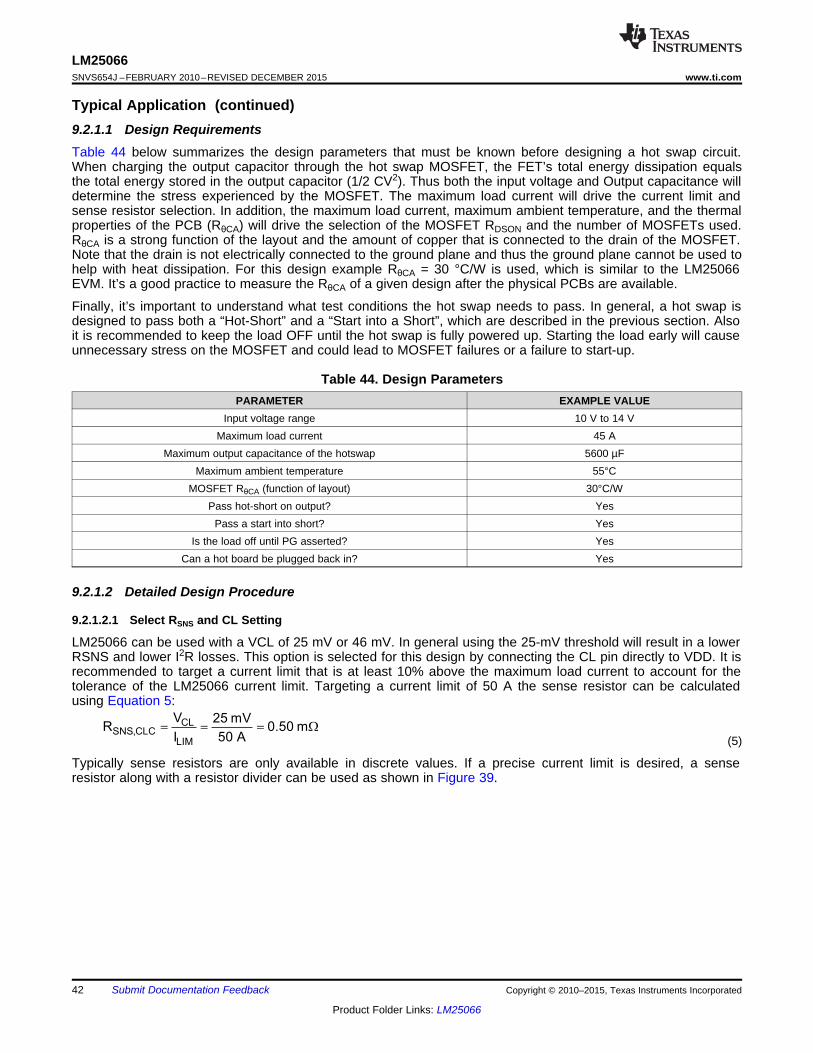
CLSNS,CLC
LIM
V 25 mVR 0.50 m
I 50 A= = = W
LM25066SNVS654J –FEBRUARY 2010–REVISED DECEMBER 2015 www.ti.com
Typical Application (continued)9.2.1.1 Design RequirementsTable 44 below summarizes the design parameters that must be known before designing a hot swap circuit.When charging the output capacitor through the hot swap MOSFET, the FET’s total energy dissipation equalsthe total energy stored in the output capacitor (1/2 CV2). Thus both the input voltage and Output capacitance willdetermine the stress experienced by the MOSFET. The maximum load current will drive the current limit andsense resistor selection. In addition, the maximum load current, maximum ambient temperature, and the thermalproperties of the PCB (RθCA) will drive the selection of the MOSFET RDSON and the number of MOSFETs used.RθCA is a strong function of the layout and the amount of copper that is connected to the drain of the MOSFET.Note that the drain is not electrically connected to the ground plane and thus the ground plane cannot be used tohelp with heat dissipation. For this design example RθCA = 30 °C/W is used, which is similar to the LM25066EVM. It’s a good practice to measure the RθCA of a given design after the physical PCBs are available.
Finally, it’s important to understand what test conditions the hot swap needs to pass. In general, a hot swap isdesigned to pass both a “Hot-Short” and a “Start into a Short”, which are described in the previous section. Alsoit is recommended to keep the load OFF until the hot swap is fully powered up. Starting the load early will causeunnecessary stress on the MOSFET and could lead to MOSFET failures or a failure to start-up.
Table 44. Design ParametersPARAMETER EXAMPLE VALUE
Input voltage range 10 V to 14 VMaximum load current 45 A
Maximum output capacitance of the hotswap 5600 µFMaximum ambient temperature 55°C
MOSFET RθCA (function of layout) 30°C/WPass hot-short on output? Yes
Pass a start into short? YesIs the load off until PG asserted? Yes
Can a hot board be plugged back in? Yes
9.2.1.2 Detailed Design Procedure
9.2.1.2.1 Select RSNS and CL Setting
LM25066 can be used with a VCL of 25 mV or 46 mV. In general using the 25-mV threshold will result in a lowerRSNS and lower I2R losses. This option is selected for this design by connecting the CL pin directly to VDD. It isrecommended to target a current limit that is at least 10% above the maximum load current to account for thetolerance of the LM25066 current limit. Targeting a current limit of 50 A the sense resistor can be calculatedusing Equation 5:
(5)
Typically sense resistors are only available in discrete values. If a precise current limit is desired, a senseresistor along with a resistor divider can be used as shown in Figure 39.
42 Submit Documentation Feedback Copyright © 2010–2015, Texas Instruments Incorporated
Product Folder Links: LM25066

2C,MAX A,MAX CA LOAD,MAX DSON JT T R I R (T )
q= + ´ ´
SNS 1SNS,EFF
1 2
R RR
R R
´
=
+
SNS,CLC1
2 SNS SNS,CLC
RR 0.5 m1
R R R 1m 0.5 m
W= = =
- W - W
RSNS
R1
R2
VIN SENSE
LM25066www.ti.com SNVS654J –FEBRUARY 2010–REVISED DECEMBER 2015
Figure 39. SENSE Resistor Divider
If using a resistor divider, then the next larger available sense resistor should be chosen (1 mΩ for example).The ratio of R1 and R2 can then be calculated using Equation 6:
(6)
Note that the SENSE pin will pull 25 μA of current, which will create an offset across R2. It is recommended tokeep R2 below 10 Ω to reduce the offset that this introduces. In addition the 1% resistors will add to the currentmonitoring error. Finally, if the resistor divider approach is used, the user should compute the effective senseresistance (RSNS,EFF) using Equation 7 and use that in all equations instead of RSNS.
(7)
Note that for many applications, a precise current limit may not be required. In that case, it’s simpler to pick thenext smaller available sense resistor. For this application, a 0.5-mΩ resistor can be used for a 50 A current limit.
9.2.1.2.2 Selecting the Hotswap FETs
It is critical to select the correct MOSFET for a hot swap design. The device must meet the followingrequirements:• The VDS rating should be sufficient to handle the maximum system voltage along with any ringing caused by
transients. For most 12-V systems a 30-V FET is a good choice.• The SOA of the FET should be sufficient to handle all usage cases: start-up, hot-short, start into short.• RDSON should be sufficiently low to maintain the junction and case temperature below the maximum rating of
the FET. In fact, it is recommended to keep the steady state FET temperature below 125°C to allow margin tohandle transients.
• Maximum continuous current rating should be above the maximum load current and the pulsed drain currentmust be greater than the current threshold of the circuit breaker. Most MOSFETs that pass the first threerequirements will also pass these two.
• A VGS rating of ± 20 V is required, because the LM25066 can pull up the gate as high as 16 V above source.– Otherwise, a diode (D3 in Figure 38) can be used to protect MOSFETs with a ± 12 V VGS rating.
For this design the CSD17556Q5B was selected for its low RDSON and good SOA. After selecting the MOSFET,the maximum steady state case temperature can be calculated using Equation 8:
(8)
Note that the RDSON is a strong function of junction temperature, which for most MOSFETs will be close to thecase temperature. A few iterations of the above equations may be necessary to converge on the final RDSON andTC,MAX value. According to the CSD17556Q5B datasheet, its RDSON is approximately 1.3x at 85°C. Equation 9uses this RDSON value to compute the TC,MAX.
Copyright © 2010–2015, Texas Instruments Incorporated Submit Documentation Feedback 43
Product Folder Links: LM25066

2 2IN,MAXOUT LIM
start 2 2LIM LIM
VC P 5600 F (14 V) 112 Wt 5.03 ms
2 P 2 112 WI (50 A)
é ù é ùmê ú= ´ + = ´ + =ê úê ú ê úë ûë û
OUT IN,MAXstart,max
LIM
C Vt
I
´
=
5
PWR
14 VR 1.94 10 0.5 m 112 W 2.1mV 5.16 k
0.5 m
æ ö= ´ ´ W - ´ = Wç ÷
Wè ø
5 DSPWR SNS LIM
SNS
VR 1.94 10 R P 2.1mV
R
æ ö= ´ ´ - ´ç ÷
è ø
SNS,MIN IN,MAXLIM,MIN
SNS
V V 4 mV 14 VP 112 W
R 0.5 m
´ ´= = =
W
LIM SNSSNS
DS
P RV
V
´
=
2
C,MAX
C 45 AT 55 C 30 (1.3 1.4 m ) 82.6 C
W 2
æ ö= ° + ° ´ ´ ´ W = °ç ÷
è ø
2LOAD,MAX
C,MAX A,MAX CA DSON J
IT T R R (T )
# of MOSFETsq
æ ö= + ´ ´ç ÷
è ø
2C,MAX
CT 55 C 30 (45 A) (1.3 1.4 m ) 165.6 C
W= ° + ° ´ ´ ´ W = °
LM25066SNVS654J –FEBRUARY 2010–REVISED DECEMBER 2015 www.ti.com
(9)
This maximum steady state case temperature indicates that a second MOSFET may be needed to reduce anddistribute power dissipation during normal operation. When using parallel MOSFETs, the maximum steady statecase temperature can be calculated using Equation 10:
(10)
Thus using two of the CSD17556Q5B in parallel will result in a steady state temperature of:
(11)
Note that the computed TC,MAX is close to the junction temperature assumed for RDSON. Thus no further iterationsare necessary.
9.2.1.2.3 Select Power Limit
In general, a lower power limit setting is preferred to reduce the stress on the MOSFET. However, when theLM25066 is set to a very low power limit setting, it has to regulate the FET current and hence the voltage acrossthe sense resistor (VSNS) to a very low value. VSNS can be calculated using Equation 12:
(12)
To avoid significant degradation of the power limiting a VSNS of less than 4 mV is not recommended. Based onthis requirement the minimum allowed power limit can be calculated using Equation 13:
(13)
In most applications the power limit can be set to PLIM,MIN using Equation 14. Here RSNS and RPWR are in Ωs andPLIM is in Watts.
(14)
So note that the minimum RPWR would occur when VDS = VIN,MAX. We can then calculate the minimum RPWRusing Equation 15:
(15)
The next largest available resistor should be selected. In this case a 5.23-kΩ resistor was chosen, which sets a112.72 W power limit.
9.2.1.2.4 Set Fault Timer
The fault timer runs when the hot swap is in power limit or current limit, which is the case during start-up. Thusthe timer has to be sized large enough to prevent a time-out during start-up. If the device starts directly intocurrent limit (ILIM) × VDS < PLIM) the maximum start time can be calculated using Equation 16:
(16)
For most designs (including this example) ILIM × VDS > PLIM so the hot swap will start in power limit and transitioninto current limit. In that case the estimated start time can be calculated using Equation 17:
(17)
44 Submit Documentation Feedback Copyright © 2010–2015, Texas Instruments Incorporated
Product Folder Links: LM25066

J,ABSMAX C,MAXSOA C,MAX SOA
J,ABSMAX
T TI (10.58 ms,T ) I (10.58 ms,25 C)
T 25 C
150 C 82.6 C9.71 A 5.24 A
150 C 25 C
-= ° ´
- °
° - °= ´ =
° - °
0.523 0.523SOAI (10.58 ms) 10 A (10 ms) (10.58 ms) 9.71 A-
= ´ ´ =
0.523SOA 1m 0.5231
I (t ) 10 Aa 10 A (10 ms)
t (10 ms)-
= = = ´
SOA 1 SOA 2
1 2
10 AIn
3 AIn(I (t ) / I (t )m 0.523
In(t / t ) 10 msIn
100 ms
æ öç ÷è ø= = = -
æ öç ÷è ø
mSOAI (t) a t= ´
TIMER timerflt
timer
C v 560 nF 1.7 Vt 10.58 ms
i 90 A
´ ´= = =
m
flt timerTIMER
timer
t i 10.06 ms 90 AC 533 nF
V 1.7 V
´ ´ m= = =
LM25066www.ti.com SNVS654J –FEBRUARY 2010–REVISED DECEMBER 2015
Note that the above start-time assumes constant, typical current limit and power limit values. The actual start-uptime will be slightly longer, as the power limit is a function of VDS and will decrease as the output voltageincreases. To ensure that the timer never times out during start-up, it is recommended to set the fault time (tflt) tobe 2 × tstart or 10.06 ms. This will account for the variation in power limit, timer current, and timer capacitance.Thus CTIMER can be calculated using Equation 18:
(18)
The next largest available CTIMER is chosen as 560 nF. Once the CTIMER is chosen the actual programmed faulttime can be calculated using Equation 19:
(19)
9.2.1.2.5 Check MOSFET SOA
Once the power limit and fault timer are chosen, it’s critical to check that the FET will stay within its SOA duringall test conditions. During a “Hot-Short” the circuit breaker will trip and the LM25066 will restart into power limituntil the timer runs out. In the worst case the MOSFET’s VDS will equal VIN,MAX, IDS will equal PLIM / VIN,MAX andthe stress event will last for tflt. For this design example the MOSFET will have 14 V, 8 A across it for 10.58 ms.
Based on the SOA of the CSD17556Q5B, it can handle 14 V, 10 A for 10 ms and it can handle 14 V, 3 A for100 ms. The SOA for 10.58 ms can be extrapolated by approximating SOA vs time as a power function asshown in Equation 20 through Equation 23:
(20)
(21)
(22)
(23)
Note that the SOA of a MOSFET is specified at a case temperature of 25°C, while the case temperature can bemuch hotter during a hot-short. The SOA should be de-rated based on TC,MAX using Equation 24:
(24)
Based on this calculation the MOSFET can handle 5.24 A, 14 V for 10.58 ms at elevated case temperature, butis required to handle 8 A during a hot-short. This means the MOSFET will be at risk of getting damaged during ahot-short. In general, it is recommended for the MOSFET to be able to handle a minimum of 1.3x more powerthan what is required during a hot-short in order to provide margin to cover the variance of the power limit andfault time.
9.2.1.2.6 Switching to dV/dt based Start-up
For designs with large load currents and output capacitances, using a power limit based start-up can beimpractical. Fundamentally, increasing load currents will reduce the sense resistor, which will increase theminimum power limit. Using a larger output capacitor will result in a longer start-up time and require a longer faulttimer. Thus a longer fault timer and a larger power limit setting are required, which places more stress on theMOSFET during a hot-short or a start into short. Eventually, there will be no FETs that can support such arequirement.
Copyright © 2010–2015, Texas Instruments Incorporated Submit Documentation Feedback 45
Product Folder Links: LM25066
J,ABSMAX C,MAXSOA C,MAX SOA
J,ABSMAX
T T 150 C 82.6 CI (28 ms,T ) I (28 ms,25 C) 5.84 A 3.15 A
T 25 C 150 C 25 C
- ° - °= ° ´ = ´ =
- ° ° - °
SOURCEOUT,dV/dt
dv/dt
I 22 AV 0.22 V / ms
C 100 nF
m= = =
SOURCE,MAXdV/dt
I 22 Ac 88 nF
0.25 V / ms 0.25 V / ms
m= = =
J,ABSMAX A,MAXSOA A,MAX SOA
J,ABSMAX
T T 150 C 55 CI (28 ms,T ) I (28 ms,25 C) 5.84 A 4.44 A
T 25 C 150 C 25 C
- ° - °= ° ´ = ´ =
- ° ° - °
0.523 0.523SOAI (28 ms) 10 A (10 ms) (28 ms) 5.84 A-
= ´ ´ =
OUTINR OUT
dV 0.25 VI C 5600 F 1.4 A
dt ms= ´ = m ´ =
LM25066SNVS654J –FEBRUARY 2010–REVISED DECEMBER 2015 www.ti.com
To avoid this problem, a dV/dt limiting capacitor (CdV/dt) can be used to limit the slew rate of the gate and theoutput voltage. The inrush current can be set arbitrarily small by reducing the slew rate of the VOUT. In addition,the power limit is set to satisfy the minimum power limit requirement and to keep the timer from running duringstart-up (make PLIM / VIN,MAX > IINR). Since the timer doesn’t run during start-up it can be made small to reducethe stress that the MOSFET experiences during a start into short or a hot-short.
The D2 prevents the charge of CdV/dt from interfering with the power limit loop during a hot-short event and Q3discharges CdV/dt when the hot swap gate comes down.
9.2.1.2.7 Choosing the VOUT Slew Rate
The inrush current should be kept low enough to keep the MOSFET within its SOA during start-up. Note that thetotal energy dissipated in the MOSFET during start-up is constant regardless of the inrush time. Thus, stretchingit out over a longer time will always reduce the stress on the MOSFET as long as the load is off during start-up.
When choosing a target slew rate, one should pick a reasonable number, check the SOA and reduce the slewrate if necessary. Using 0.25 V/ms as a starting point the inrush current can be computed as follows:
(25)
Assuming a maximum input voltage of 14 V, it will take 56 ms to start-up. Note that the power dissipation of theFET will start at VIN,MAX × IINR and reduce to zero as the VDS of the MOSFET is reduced. Note that the SOAcurves assume the same power dissipation for a given time. A conservative approach is to assume an equivalentpower profile where PFET = VIN,MAX × IINR for t = tstart-up /2. In this instance, the SOA can be checked by looking ata 14 V, 1.4 A, 28 ms pulse. Using the same technique as Check MOSFET SOA, the MOSFET SOA can beestimated with Equation 26.
(26)
This value has to also be derated for temperature. For this calculation, it is assumed that TC can equal TA,MAXwhen the board is plugged in. This would occur if a board is plugged in at an elevated ambient temperatureenvironment.
(27)
Based on this calculation the MOSFET can handle 4.44 A, 14 V for 28 ms at elevated ambient temperature, andis required to handle 1.4 A. This indicates the MOSFET will stay well-within its SOA during a start-up if the slewrate is 0.25 V/ms or less. Note that if the load is off during start-up, the total energy dissipated in the FET isconstant regardless of the slew rate. Thus a lower slew rate will always place less stress on the FET. To ensurethat the slew rate is at most 0.25 V/ms the CdV/dt should be chosen with Equation 28.
(28)
The next largest available CdV/dt is chosen to be 100 nF. Then the typical slew rate and start time can becomputed to be 0.22 V/ms as shown below, making the typical start time 55 ms, assuming 12 V input.
(29)
In certain applications, TC,MAX may be used for temperature derating instead. This would only occur if a hot boardis unplugged and then plugged back in before it cools off to ambient temperature. This is worst case and formany applications, the TA,MAX can be used for this derating.
(30)
Based on this calculation using TC,MAX for derating, the MOSFET can handle 3.15 A, 14 V for 28 ms at elevatedcase temperature, and is required to handle 1.4 A. This indicates the MOSFET will stay well-within its SOAduring a start-up if the slew rate is 0.25 V/ms or less.
46 Submit Documentation Feedback Copyright © 2010–2015, Texas Instruments Incorporated
Product Folder Links: LM25066

( )SOA C,MAX
175 C 114 CI 0.52ms, T 42.3A 17.17A
175 C 25 C
° - °= ´ =
° - °
0.52 0.52SOAI (0.52 ms,25 C) 30 A (ms) (0.52 ms) 42.3 A-
° = ´ ´ =
0.52SOA 2
m 0.522
I (t ) 30 Aa 30 A (ms)
t (1ms)-
= = = ´
SOA 1 SOA 2
1 2
100 AIn
30 AIn(I (t ) / I (t )m 0.52
In(t / t ) 0.1msIn
1ms
æ öç ÷è ø= = = -æ öç ÷è ø
mSOAI (t) a t= ´
5
PWR SNS LIM
SNS
5
VdsR 1.94 10 R P 2.1mV
R
14 V1.94 10 0.5 m 112 W 2.1mV 5.16 k
0.5 m
æ ö= ´ ´ - ´ç ÷
è ø
æ ö= ´ ´ W - ´ = Wç ÷
Wè ø
SNS,MIN IN,MAXLIM,MIN IN,MAX INR,MAX
SNS
V VP max ,2 V I max (112 W,39.2 W) 112 W
R
´æ ö= ´ ´ = =ç ÷
è ø
LM25066www.ti.com SNVS654J –FEBRUARY 2010–REVISED DECEMBER 2015
9.2.1.2.8 Select Power Limit and Fault Timer
When picking the power limit, it needs to meet 2 requirements:1. Power limit is large enough to avoid operating with VSNS < 4 mV2. Power limit is large enough to ensure that the timer doesn’t run during start up. Picking a power limit such
that it is 2x of IINR,MAX × VIN,MAX is good practice.
Thus the minimum allowed power limit can be computed with Equation 31.
(31)
Next, the power limit is set to PLIM,MIN using the equation below. Here RSNS and RPWR are in Ωs and PLIM isin Watts.
(32)
The closest available resistor should be selected. In this case a 5.23-kΩ resistor was chosen.
Next a fault timer value should be selected. In general, the timer value should be decreased until there is enoughmargin between available SOA and the power pulse the FET experiences during a hot-short. For this design a22-nF CTIMER was chosen corresponding to a 420-µs fault time. The available SOA is extrapolated using themethod described earlier.
(33)
(34)
(35)
(36)
Next the available SOA is derated for temperature:
(37)
Note that only 4 A was required, while the FET can support 17.17A. This confirms that the design will be robustand have plenty of margin.
9.2.1.2.9 Set Undervoltage and Overvoltage Threshold
By programming the UVLO and OVLO thresholds the LM25066 enables the series pass device (Q1) when theinput supply voltage (VSYS) is within the desired operational range. If VSYS is below the UVLO threshold, or abovethe OVLO threshold, Q1 is switched off, denying power to the load. Hysteresis is provided for each threshold.
9.2.1.2.9.1 Option A
The configuration shown in Figure 40 requires three resistors (R1-R3) to set the thresholds.
Copyright © 2010–2015, Texas Instruments Incorporated Submit Documentation Feedback 47
Product Folder Links: LM25066

VOVH =1.16V x (R1 + R2 + R3)
R3
VUVL =1.16V x (R1 + R2 + R3)
R2 + R3
VUVH = 1.16V + [R1 x (23 PA +(R2 + R3)
1.16V)]
R2 =1.16V x R1
(7V ± 1.16V)- R3 = 4.61 k:
R3 =1.16V x R1 x 7V
15V x (7V - 1.16V)= 4.03 k:
R1 =8V - 7V23 PA
=1V
= 43.5 k:23 PA
VOVL = [(R1 + R2) x ((1.16V) - 23 PA)] + 1.16VR3
R2 =1.16V x R1VUVL - 1.16V
- R3
R3 =1.16V x R1 x VUVL
VOVH x (VUVL ± 1.16V)
R1 =VUVH - VUVL
23 PA=
VUV(HYS)
23 PA
VIN
UVLO/EN
OVLO
GND
R1
R2
R3
1.16V
1.16V
23 PA
TIMER AND GATE
LOGIC CONTROL
LM25066
VSYS
23PA
LM25066SNVS654J –FEBRUARY 2010–REVISED DECEMBER 2015 www.ti.com
Figure 40. UVLO and OVLO Thresholds Set By R1-R3
The procedure to calculate the resistor values is as follows:• Choose the upper UVLO threshold (VUVH), and the lower UVLO threshold (VUVL).• Choose the upper OVLO threshold (VOVH).• The lower OVLO threshold (VOVL) cannot be chosen in advance in this case, but is determined after the
values for R1-R3 are determined. If VOVL must be accurately defined in addition to the other three thresholds,see Option B below. The resistors are calculated as follows:
(38)
(39)
(40)The lower OVLO threshold is calculated from:
(41)As an example, assume the application requires the following thresholds: VUVH = 8 V, VUVL = 7 V, VOVH = 15V.
(42)
(43)
(44)The lower OVLO threshold calculates to 12.03 V and the OVLO hysteresis is 2.97 V. Note that the OVLOhysteresis is always slightly greater than the UVLO hysteresis in this configuration. When the R1-R3 resistorvalues are known, the threshold voltages and hysteresis are calculated from the following:
(45)
(46)VUV(HYS) = R1 × 23µA (47)
(48)
48 Submit Documentation Feedback Copyright © 2010–2015, Texas Instruments Incorporated
Product Folder Links: LM25066

VOVL = 1.16V + [R3 x (1.16V - 23 PA)]R4
VOVH =1.16V x (R3 + R4)
R4
VUVL =1.16V x (R1 + R2)
R2
VUVH = 1.16V + [R1 x (1.16V + 23 PA)]R2
R4 =(VOVH - 1.16V)
1.16V x R3
R3 =VOVH - VOVL
23 PA=
VOV(HYS)
23 PA
R2 =(VUVL - 1.16V)
1.16V x R1
R1 =VUVH - VUVL
23 PA=
VUV(HYS)
23 PA
VIN
UVLO/EN
OVLO
GND
R1
R3
R4
1.16V
1.16V
23 PA
TIMER AND GATE
LOGIC CONTROL
LM25066
VSYS
23PA
R2
VOVL = [(R1 + R2) x ( - 23 PA)] + 1.16VR3
1.16V
LM25066www.ti.com SNVS654J –FEBRUARY 2010–REVISED DECEMBER 2015
(49)VOV(HYS) = (R1 + R2) × 23µA (50)
9.2.1.2.9.2 Option B
If all four thresholds must be accurately defined, the configuration in Figure 41 can be used.
Figure 41. Programming the Four Thresholds
The four resistor values are calculated as follows:• Choose the upper and lower UVLO thresholds (VUVH) and (VUVL).
(51)
(52)• Choose the upper and lower OVLO threshold (VOVH) and (VOVL).
(53)
(54)
As an example, assume the application requires the following thresholds: VUVH = 8 V, VUVL = 7 V, VOVH = 15.5 V,and VOVL = 14 V. Therefore VUV(HYS) = 1 V and VOV(HYS) = 1.5 V. The resistor values are:
R1 = 43.5 kΩ, R2 = 8.64 kΩ (55)R3 = 65.2 kΩ, R4 = 5.27 kΩ (56)
When the R1-R4 resistor values are known, the threshold voltages and hysteresis are calculated from thefollowing:
(57)
(58)VUV(HYS) = R1 × 23 µA (59)
(60)
(61)VOV(HYS) = R3 × 23 µA (62)
Copyright © 2010–2015, Texas Instruments Incorporated Submit Documentation Feedback 49
Product Folder Links: LM25066

OVH
1.16 V R3 1.16 V 43.48 kR4 3.65 k
(V 1.16 V) (15 V 1.16 V)
´ ´ W= = = W
- -
OVH OVLV V 15 V 14 VR3 43.48 k
23 A 23 A
- -= = = W
m m
UVL
1.16 V R1 1.16 V 43.48 kR2 6.49 k
(V 1.16 V) (9 V 1.16 V)
´ ´ W= = = W
- -
UVH UVLV V 10 V 9 VR1 43.48 k
23 A 23 A
- -= = = W
m m
VIN
UVLO/EN
OVLO
GND
10k
R3
R4
1.16V
1.16V
23 PA
TIMER AND GATE
LOGIC CONTROL
LM25066
VSYS
23PA
LM25066SNVS654J –FEBRUARY 2010–REVISED DECEMBER 2015 www.ti.com
9.2.1.2.9.3 Option C
The minimum UVLO level is obtained by connecting the UVLO/EN pin to VIN as shown in Figure 42. Q1 isswitched on when the VIN voltage reaches the POR threshold (≊ 2.6 V). The OVLO thresholds are set using R3,R4. Their values are calculated using the procedure in Option B.
Figure 42. UVLO = POR
9.2.1.2.9.4 Option D
The OVLO function can be disabled by grounding the OVLO pin. The UVLO thresholds are set as described inOption B or Option C.
For this design example option B is used and the following values are targeted: VUVH = 10 V, VUVL = 9 V,VOVH = 15 V, VOVL = 14 V. R1, R2, R3, and R4 are computed using the equations below:
(63)
(64)
(65)
(66)
Nearest available 1% resistors should be chosen. Set R1 = 43.2 kΩ, R2 = 6.49 kΩ, R3 = 43.2 kΩ, and R4 = 3.65kΩ.
9.2.1.2.10 Power Good Pin
When the voltage at the FB pin increases above its threshold, the internal pulldown acting on the PGD pin isdisabled allowing PGD to rise to VPGD through the pullup resistor, RPG, as shown in Figure 44. The pullup voltage(VPGD) can be as high as 17 V, and can be higher or lower than the voltages at VIN and OUT. VDD is aconvenient choice for VPGD as it allows interface to low voltage logic and avoids glitching on PGD during power-up. If a delay is required at PGD, suggested circuits are shown in Figure 45. In Figure 45A capacitor CPG addsdelay to the rising edge, but not to the falling edge. In Figure 45B, the rising edge is delayed by RPG1 + RPG2 andCPG, while the falling edge is delayed a lesser amount by RPG2 and CPG. Adding a diode across RPG2(Figure 45C) allows for equal delays at the two edges, or a short delay at the rising edge and a long delay at thefalling edge.
Setting the output threshold for the PGD pin requires two resistors (R4, R5) as shown in Figure 43. Whilemonitoring the output voltage is shown in Figure 43, R4 can be connected to any other voltage which requiresmonitoring.
The resistor values are calculated as follows:
Choose the upper and lower threshold (VPGDH) and (VPGDL) at VOUT.
50 Submit Documentation Feedback Copyright © 2010–2015, Texas Instruments Incorporated
Product Folder Links: LM25066

GND
LM25066 RPG1
VPGD
CPG
PGD
GND
LM25066 RPG1
Power Good
VPGD
CPG
PGD
RPG2
GND
LM25066RPG1
VPGD
CPG
PGD
RPG2
C) Short Delay at Rising Edge and Long Delay at Falling Edge or Equal Delays
B) Long Delay at Rising Edge, Short Delay at Falling Edge
A) Delay at Rising Edge Only
Power Good
Power Good
GND
LM25066 RPG
Power Good
VPGD
OUT
FB
GND
PGD
GATE
from UVLO
from OVLO
1.167V
24 PA
Q1VOUT
R 4
R 5
LM25066
R4 =VPGDH - VPGDL
24 PA=
VPGD(HYS)
24 PA
R5 =1.167V x R4
(VPGDH - 1.167V)
LM25066www.ti.com SNVS654J –FEBRUARY 2010–REVISED DECEMBER 2015
(67)
Figure 43. Programming the PGD Threshold
Figure 44. Power Good Output
Figure 45. Adding Delay to the Power Good Output Pin
For this example PGDH of 9.25 V and PGDL of 8.75 V is targeted. R5 and R6 are computed using the equationsbelow:
Copyright © 2010–2015, Texas Instruments Incorporated Submit Documentation Feedback 51
Product Folder Links: LM25066

LM25066
Inductive
Load
VIN
GND
+12V
GND
LIVEPOWER
SOURCE
PLUG-IN BOARD
OUT
RS Q1 VOUT
SENSETVSD1
SchottkyD2
VSYS
GATE CL
PGDH
1.167 V R5 1.167 V 10.42 kR6 1.55 k
(V 1.167 V) (9.25 V 1.167 V)
´ ´ W= = = W
- -
PGDH PGDLV V 9.25 V 8.75 VR5 10.42 k
24 A 24 A
- -= = = W
m m
LM25066SNVS654J –FEBRUARY 2010–REVISED DECEMBER 2015 www.ti.com
(68)
(69)
Nearest available 1% resistors should be chosen. Set R5 = 10 kΩ and R6 = 1.5 kΩ.
9.2.1.2.11 Input and Output Protection
Proper operation of the LM25066 hot swap circuit requires a voltage clamping element present on the supplyside of the connector into which the hot swap circuit is plugged in. A TVS is ideal, as depicted in Figure 46. TheTVS is necessary to absorb the voltage transient generated whenever the hot swap circuit shuts off the loadcurrent. This effect is the most severe during a hot-short when a large current is suddenly interrupted when theFET shuts off. The TVS should be chosen to have minimal leakage current at VIN,MAX and to clamp the voltage tounder 24 V during hot-short events. For many high power applications, 5.0SMDJ13A is a good choice.
If the load powered by the LM25066 hot swap circuit has inductive characteristics, a Schottky diode is requiredacross the LM25066's output, along with some load capacitance. The capacitance and the diode are necessaryto limit the negative excursion at the OUT pin when the load current is shut off.
Figure 46. Output Diode Required for Inductive Loads
9.2.1.2.12 Final Schematic and Component Values
Figure 38 shows the schematic used to implement the requirements described in the previous section. Inaddition, Table 45 provides the final component values that were used to meet the design requirements for a12-V, 45-A hot swap design. The application curves in the next section are based on these component values.
Table 45. Final Component Values (12-V, 45-A Design)COMPONENT VALUE
RSNS 0.5 mΩR1, R3 43.2 kΩ
R2 6.49 kΩR4 3.65 kΩ
RFB1 10 kΩRFB2 1.5 kΩRPWR 5.11 kΩ
Q1 CSD17556Q5BQ2 MMBT3904Q3 MMBT3906
D1, D3 1N4148W-7-FD2 SK153-TP
52 Submit Documentation Feedback Copyright © 2010–2015, Texas Instruments Incorporated
Product Folder Links: LM25066

LM25066www.ti.com SNVS654J –FEBRUARY 2010–REVISED DECEMBER 2015
Table 45. Final Component Values (12-V, 45-A Design) (continued)COMPONENT VALUE
Z1 5.0MDJA15ACdV/dt 100 nF
CTIMER 22 nF
9.2.2 Application Curves
VIN = 12 V
Figure 47. Start-Up Figure 48. Start-Up into Short
Figure 49. Undervoltage Figure 50. Overvoltage
Figure 52. LoadstepFigure 51. Gradual Overcurrent
Copyright © 2010–2015, Texas Instruments Incorporated Submit Documentation Feedback 53
Product Folder Links: LM25066
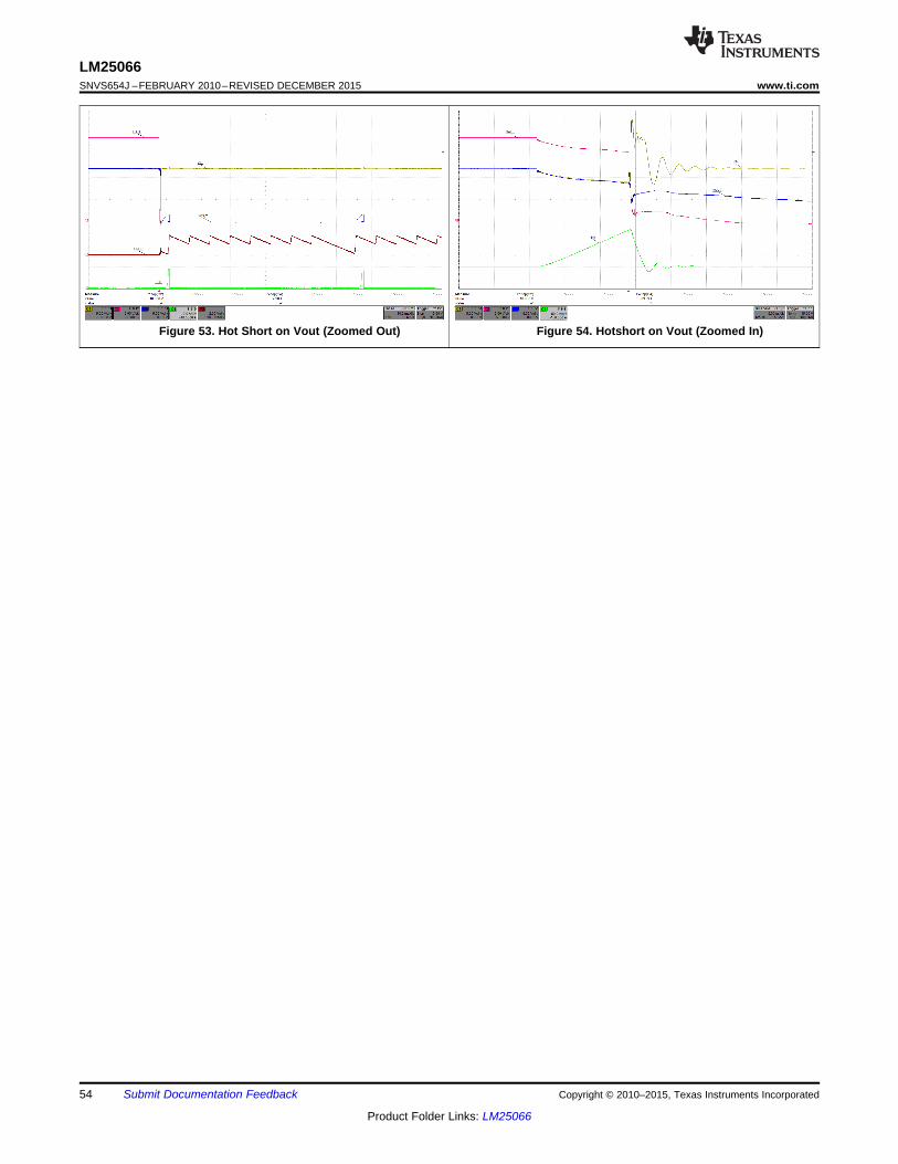
LM25066SNVS654J –FEBRUARY 2010–REVISED DECEMBER 2015 www.ti.com
Figure 53. Hot Short on Vout (Zoomed Out) Figure 54. Hotshort on Vout (Zoomed In)
54 Submit Documentation Feedback Copyright © 2010–2015, Texas Instruments Incorporated
Product Folder Links: LM25066
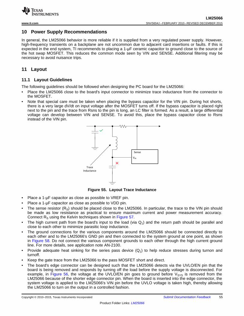
VIN
Sense
Trace
Inductance
LM25066www.ti.com SNVS654J –FEBRUARY 2010–REVISED DECEMBER 2015
10 Power Supply RecommendationsIn general, the LM25066 behavior is more reliable if it is supplied from a very regulated power supply. However,high-frequency transients on a backplane are not uncommon due to adjacent card insertions or faults. If this isexpected in the end system, TI recommends to placing a 1-μF ceramic capacitor to ground close to the source ofthe hot swap MOSFET. This reduces the common mode seen by VIN and SENSE. Additional filtering may benecessary to avoid nuisance trips.
11 Layout
11.1 Layout GuidelinesThe following guidelines should be followed when designing the PC board for the LM25066:• Place the LM25066 close to the board's input connector to minimize trace inductance from the connector to
the MOSFET.• Note that special care must be taken when placing the bypass capacitor for the VIN pin. During hot shorts,
there is a very large dV/dt on input voltage after the MOSFET turns off. If the bypass capacitor is placed rightnext to the pin and the trace from Rsns to the pin is long, an LC filter is formed. As a result, a large differentialvoltage can develop between VIN and SENSE. To avoid this, place the bypass capacitor close to Rsnsinstead of the VIN pin.
Figure 55. Layout Trace Inductance
• Place a 1-µF capacitor as close as possible to VREF pin.• Place a 1-µF capacitor as close as possible to VDD pin.• The sense resistor (RS) should be placed close to the LM25066. In particular, the trace to the VIN pin should
be made as low resistance as practical to ensure maximum current and power measurement accuracy.Connect RS using the Kelvin techniques shown in Figure 57.
• The high current path from the board's input to the load (via Q1) and the return path should be parallel andclose to each other to minimize parasitic loop inductance.
• The ground connections for the various components around the LM25066 should be connected directly toeach other and to the LM25066's GND pin and then connected to the system ground at one point, as shownin Figure 58. Do not connect the various component grounds to each other through the high current groundline. For more details, see application note AN-2100.
• Provide adequate heat sinking for the series pass device (Q1) to help reduce stresses during turnon andturnoff.
• Keep the gate trace from the LM25066 to the pass MOSFET short and direct.• The board's edge connector can be designed such that the LM25066 detects via the UVLO/EN pin that the
board is being removed and responds by turning off the load before the supply voltage is disconnected. Forexample, in Figure 56, the voltage at the UVLO/EN pin goes to ground before VSYS is removed from theLM25066 because of the shorter edge connector pin. When the board is inserted into the edge connector, thesystem voltage is applied to the LM25066's VIN pin before the UVLO voltage is taken high, thereby allowingthe LM25066 to turn on the output in a controlled fashion.
Copyright © 2010–2015, Texas Instruments Incorporated Submit Documentation Feedback 55
Product Folder Links: LM25066

Hot Swap
R R
C
C C
Rsns
Output CapsSource
R
R
IC GND
High Current GND
SENSERESISTOR
RS
VIN SENSE
FROM SYSTEM INPUT VOLTAGE
TO DRAIN OF
MOSFET Q1
HIGH CURRENT PATH
Q1R1
R2
R3
ToLoad
RS
CARD EDGE CONNECTOR
PLUG-IN CARD
VSYS
GND
OUTPGDPWR
TIMERRETRY
SCLSMBAVREFDIODEVAUX
SE
NS
EG
AT
E
VIN
UV
LOO
VLO
GN
DS
DA
CB
FBCL
VD
DA
DD
0A
DD
1A
DD
2
LM25066
LM25066SNVS654J –FEBRUARY 2010–REVISED DECEMBER 2015 www.ti.com
11.2 Layout Example
Figure 56. Recommended Board Connector Design
Figure 57. Sense Resistor Connections
Figure 58. LM25066 Quiet IC Ground Layout56 Submit Documentation Feedback Copyright © 2010–2015, Texas Instruments Incorporated
Product Folder Links: LM25066

LM25066www.ti.com SNVS654J –FEBRUARY 2010–REVISED DECEMBER 2015
12 Device and Documentation Support
12.1 Device Support
12.1.1 Development SupportFor the LM25066 Design Calculator, go to http://www.ti.com/product/LM25066/toolssoftware.
12.2 Community ResourcesThe following links connect to TI community resources. Linked contents are provided "AS IS" by the respectivecontributors. They do not constitute TI specifications and do not necessarily reflect TI's views; see TI's Terms ofUse.
TI E2E™ Online Community TI's Engineer-to-Engineer (E2E) Community. Created to foster collaborationamong engineers. At e2e.ti.com, you can ask questions, share knowledge, explore ideas and helpsolve problems with fellow engineers.
Design Support TI's Design Support Quickly find helpful E2E forums along with design support tools andcontact information for technical support.
12.3 TrademarksE2E is a trademark of Texas Instruments.All other trademarks are the property of their respective owners.
12.4 Electrostatic Discharge CautionThese devices have limited built-in ESD protection. The leads should be shorted together or the device placed in conductive foamduring storage or handling to prevent electrostatic damage to the MOS gates.
12.5 GlossarySLYZ022 — TI Glossary.
This glossary lists and explains terms, acronyms, and definitions.
13 Mechanical, Packaging, and Orderable InformationThe following pages include mechanical, packaging, and orderable information. This information is the mostcurrent data available for the designated devices. This data is subject to change without notice and revision ofthis document. For browser-based versions of this data sheet, refer to the left-hand navigation.
Copyright © 2010–2015, Texas Instruments Incorporated Submit Documentation Feedback 57
Product Folder Links: LM25066

PACKAGE OPTION ADDENDUM
www.ti.com 16-Jan-2015
Addendum-Page 1
PACKAGING INFORMATION
Orderable Device Status(1)
Package Type PackageDrawing
Pins PackageQty
Eco Plan(2)
Lead/Ball Finish(6)
MSL Peak Temp(3)
Op Temp (°C) Device Marking(4/5)
Samples
LM25066PSQ/NOPB ACTIVE WQFN NHZ 24 1000 Green (RoHS& no Sb/Br)
CU SN Level-3-260C-168 HR -40 to 125 L25066P
LM25066PSQE/NOPB ACTIVE WQFN NHZ 24 250 Green (RoHS& no Sb/Br)
CU SN Level-3-260C-168 HR -40 to 125 L25066P
LM25066PSQX/NOPB ACTIVE WQFN NHZ 24 4500 Green (RoHS& no Sb/Br)
CU SN Level-3-260C-168 HR -40 to 125 L25066P
(1) The marketing status values are defined as follows:ACTIVE: Product device recommended for new designs.LIFEBUY: TI has announced that the device will be discontinued, and a lifetime-buy period is in effect.NRND: Not recommended for new designs. Device is in production to support existing customers, but TI does not recommend using this part in a new design.PREVIEW: Device has been announced but is not in production. Samples may or may not be available.OBSOLETE: TI has discontinued the production of the device.
(2) Eco Plan - The planned eco-friendly classification: Pb-Free (RoHS), Pb-Free (RoHS Exempt), or Green (RoHS & no Sb/Br) - please check http://www.ti.com/productcontent for the latest availabilityinformation and additional product content details.TBD: The Pb-Free/Green conversion plan has not been defined.Pb-Free (RoHS): TI's terms "Lead-Free" or "Pb-Free" mean semiconductor products that are compatible with the current RoHS requirements for all 6 substances, including the requirement thatlead not exceed 0.1% by weight in homogeneous materials. Where designed to be soldered at high temperatures, TI Pb-Free products are suitable for use in specified lead-free processes.Pb-Free (RoHS Exempt): This component has a RoHS exemption for either 1) lead-based flip-chip solder bumps used between the die and package, or 2) lead-based die adhesive used betweenthe die and leadframe. The component is otherwise considered Pb-Free (RoHS compatible) as defined above.Green (RoHS & no Sb/Br): TI defines "Green" to mean Pb-Free (RoHS compatible), and free of Bromine (Br) and Antimony (Sb) based flame retardants (Br or Sb do not exceed 0.1% by weightin homogeneous material)
(3) MSL, Peak Temp. - The Moisture Sensitivity Level rating according to the JEDEC industry standard classifications, and peak solder temperature.
(4) There may be additional marking, which relates to the logo, the lot trace code information, or the environmental category on the device.
(5) Multiple Device Markings will be inside parentheses. Only one Device Marking contained in parentheses and separated by a "~" will appear on a device. If a line is indented then it is a continuationof the previous line and the two combined represent the entire Device Marking for that device.
(6) Lead/Ball Finish - Orderable Devices may have multiple material finish options. Finish options are separated by a vertical ruled line. Lead/Ball Finish values may wrap to two lines if the finishvalue exceeds the maximum column width.
Important Information and Disclaimer:The information provided on this page represents TI's knowledge and belief as of the date that it is provided. TI bases its knowledge and belief on informationprovided by third parties, and makes no representation or warranty as to the accuracy of such information. Efforts are underway to better integrate information from third parties. TI has taken and

PACKAGE OPTION ADDENDUM
www.ti.com 16-Jan-2015
Addendum-Page 2
continues to take reasonable steps to provide representative and accurate information but may not have conducted destructive testing or chemical analysis on incoming materials and chemicals.TI and TI suppliers consider certain information to be proprietary, and thus CAS numbers and other limited information may not be available for release.
In no event shall TI's liability arising out of such information exceed the total purchase price of the TI part(s) at issue in this document sold by TI to Customer on an annual basis.

TAPE AND REEL INFORMATION
*All dimensions are nominal
Device PackageType
PackageDrawing
Pins SPQ ReelDiameter
(mm)
ReelWidth
W1 (mm)
A0(mm)
B0(mm)
K0(mm)
P1(mm)
W(mm)
Pin1Quadrant
LM25066PSQ/NOPB WQFN NHZ 24 1000 178.0 12.4 4.3 5.3 1.3 8.0 12.0 Q1
LM25066PSQE/NOPB WQFN NHZ 24 250 178.0 12.4 4.3 5.3 1.3 8.0 12.0 Q1
LM25066PSQX/NOPB WQFN NHZ 24 4500 330.0 12.4 4.3 5.3 1.3 8.0 12.0 Q1
PACKAGE MATERIALS INFORMATION
www.ti.com 20-Sep-2016
Pack Materials-Page 1
*All dimensions are nominal
Device Package Type Package Drawing Pins SPQ Length (mm) Width (mm) Height (mm)
LM25066PSQ/NOPB WQFN NHZ 24 1000 210.0 185.0 35.0
LM25066PSQE/NOPB WQFN NHZ 24 250 210.0 185.0 35.0
LM25066PSQX/NOPB WQFN NHZ 24 4500 367.0 367.0 35.0
PACKAGE MATERIALS INFORMATION
www.ti.com 20-Sep-2016
Pack Materials-Page 2

MECHANICAL DATA
NHZ0024B
www.ti.com
SQA24B (Rev A)

IMPORTANT NOTICE
Texas Instruments Incorporated and its subsidiaries (TI) reserve the right to make corrections, enhancements, improvements and otherchanges to its semiconductor products and services per JESD46, latest issue, and to discontinue any product or service per JESD48, latestissue. Buyers should obtain the latest relevant information before placing orders and should verify that such information is current andcomplete. All semiconductor products (also referred to herein as “components”) are sold subject to TI’s terms and conditions of salesupplied at the time of order acknowledgment.TI warrants performance of its components to the specifications applicable at the time of sale, in accordance with the warranty in TI’s termsand conditions of sale of semiconductor products. Testing and other quality control techniques are used to the extent TI deems necessaryto support this warranty. Except where mandated by applicable law, testing of all parameters of each component is not necessarilyperformed.TI assumes no liability for applications assistance or the design of Buyers’ products. Buyers are responsible for their products andapplications using TI components. To minimize the risks associated with Buyers’ products and applications, Buyers should provideadequate design and operating safeguards.TI does not warrant or represent that any license, either express or implied, is granted under any patent right, copyright, mask work right, orother intellectual property right relating to any combination, machine, or process in which TI components or services are used. Informationpublished by TI regarding third-party products or services does not constitute a license to use such products or services or a warranty orendorsement thereof. Use of such information may require a license from a third party under the patents or other intellectual property of thethird party, or a license from TI under the patents or other intellectual property of TI.Reproduction of significant portions of TI information in TI data books or data sheets is permissible only if reproduction is without alterationand is accompanied by all associated warranties, conditions, limitations, and notices. TI is not responsible or liable for such altereddocumentation. Information of third parties may be subject to additional restrictions.Resale of TI components or services with statements different from or beyond the parameters stated by TI for that component or servicevoids all express and any implied warranties for the associated TI component or service and is an unfair and deceptive business practice.TI is not responsible or liable for any such statements.Buyer acknowledges and agrees that it is solely responsible for compliance with all legal, regulatory and safety-related requirementsconcerning its products, and any use of TI components in its applications, notwithstanding any applications-related information or supportthat may be provided by TI. Buyer represents and agrees that it has all the necessary expertise to create and implement safeguards whichanticipate dangerous consequences of failures, monitor failures and their consequences, lessen the likelihood of failures that might causeharm and take appropriate remedial actions. Buyer will fully indemnify TI and its representatives against any damages arising out of the useof any TI components in safety-critical applications.In some cases, TI components may be promoted specifically to facilitate safety-related applications. With such components, TI’s goal is tohelp enable customers to design and create their own end-product solutions that meet applicable functional safety standards andrequirements. Nonetheless, such components are subject to these terms.No TI components are authorized for use in FDA Class III (or similar life-critical medical equipment) unless authorized officers of the partieshave executed a special agreement specifically governing such use.Only those TI components which TI has specifically designated as military grade or “enhanced plastic” are designed and intended for use inmilitary/aerospace applications or environments. Buyer acknowledges and agrees that any military or aerospace use of TI componentswhich have not been so designated is solely at the Buyer's risk, and that Buyer is solely responsible for compliance with all legal andregulatory requirements in connection with such use.TI has specifically designated certain components as meeting ISO/TS16949 requirements, mainly for automotive use. In any case of use ofnon-designated products, TI will not be responsible for any failure to meet ISO/TS16949.
Products ApplicationsAudio www.ti.com/audio Automotive and Transportation www.ti.com/automotiveAmplifiers amplifier.ti.com Communications and Telecom www.ti.com/communicationsData Converters dataconverter.ti.com Computers and Peripherals www.ti.com/computersDLP® Products www.dlp.com Consumer Electronics www.ti.com/consumer-appsDSP dsp.ti.com Energy and Lighting www.ti.com/energyClocks and Timers www.ti.com/clocks Industrial www.ti.com/industrialInterface interface.ti.com Medical www.ti.com/medicalLogic logic.ti.com Security www.ti.com/securityPower Mgmt power.ti.com Space, Avionics and Defense www.ti.com/space-avionics-defenseMicrocontrollers microcontroller.ti.com Video and Imaging www.ti.com/videoRFID www.ti-rfid.comOMAP Applications Processors www.ti.com/omap TI E2E Community e2e.ti.comWireless Connectivity www.ti.com/wirelessconnectivity
Mailing Address: Texas Instruments, Post Office Box 655303, Dallas, Texas 75265Copyright © 2016, Texas Instruments Incorporated