Embed Size (px)
Citation preview

LM317L3-Terminal Adjustable RegulatorGeneral DescriptionThe LM317L is an adjustable 3-terminal positive voltageregulator capable of supplying 100mA over a 1.2V to 37Voutput range. It is exceptionally easy to use and requiresonly two external resistors to set the output voltage. Further,both line and load regulation are better than standard fixedregulators. Also, the LM317L is available packaged in astandard TO-92 transistor package which is easy to use.
In addition to higher performance than fixed regulators, theLM317L offers full overload protection. Included on the chipare current limit, thermal overload protection and safe areaprotection. All overload protection circuitry remains fully func-tional even if the adjustment terminal is disconnected.
Normally, no capacitors are needed unless the device issituated more than 6 inches from the input filter capacitors inwhich case an input bypass is needed. An optional outputcapacitor can be added to improve transient response. Theadjustment terminal can be bypassed to achieve very highripple rejection ratios which are difficult to achieve with stan-dard 3-terminal regulators.
Besides replacing fixed regulators, the LM317L is useful in awide variety of other applications. Since the regulator is“floating” and sees only the input-to-output differential volt-age, supplies of several hundred volts can be regulated aslong as the maximum input-to-output differential is not ex-ceeded.
Also, it makes an especially simple adjustable switchingregulator, a programmable output regulator, or by connectinga fixed resistor between the adjustment and output, theLM317L can be used as a precision current regulator. Sup-plies with electronic shutdown can be achieved by clampingthe adjustment terminal to ground which programs the out-put to 1.2V where most loads draw little current.
The LM317L is available in a standard TO-92 transistorpackage, the SO-8 package, and 6-Bump micro SMD pack-age. The LM317L is rated for operation over a −25˚C to125˚C range.
Featuresn Adjustable output down to 1.2Vn Guaranteed 100mA output currentn Line regulation typically 0.01%Vn Load regulation typically 0.1%n Current limit constant with temperaturen Eliminates the need to stock many voltagesn Standard 3-lead transistor packagen 80dB ripple rejectionn Available in TO-92, SO-8, or 6-Bump micro SMD
packagen Output is short circuit protectedn See AN-1112 for micro SMD considerations
Connection DiagramsTO-92 Plastic package 8-Pin SOIC
0090640400906405
Top View
May 2006LM
317L3-Term
inalAdjustable
Regulator
© 2006 National Semiconductor Corporation DS009064 www.national.com

Connection Diagrams (Continued)
6-Bump micro SMD micro SMD Laser Mark
00906449
*NC = Not Internally connected.
Top View(Bump Side Down)
00906450
Ordering InformationPackage Part Number Package Marking Media Transport NSC Drawing
TO-92 LM317LZ LM317LZ 1.8k Units per Box Z03A
8-Pin SOIC LM317LM LM317LM Rails M08A
6-Bump microSMD
* LM317LIBP – 250 Units Tape and ReelBPA06HPB
* LM317LIBPX – 3k Units Tape and Reel
Note: The micro SMD package marking is a single digit manufacturing DateCode only.
LM31
7L
www.national.com 2

Absolute Maximum Ratings (Note 1)
If Military/Aerospace specified devices are required,please contact the National Semiconductor Sales Office/Distributors for availability and specifications.
Power Dissipation Internally Limited
Input-Output Voltage Differential 40V
Operating Junction TemperatureRange −40˚C to +125˚C
Storage Temperature −55˚C to +150˚C
Lead Temperature(Soldering, 4 seconds) 260˚C
Output is Short Circuit Protected
ESD Susceptibility
Human Body Model (Note 5) 2kV
Electrical Characteristics (Note 2)
Parameter Conditions Min Typ Max Units
Line Regulation TJ = 25˚C, 3V ≤ (VIN − VOUT) ≤ 40V, IL ≤ 20mA (Note 3) 0.01 0.04 %/V
Load Regulation TJ = 25˚C, 5mA ≤ IOUT ≤ IMAX, (Note 3) 0.1 0.5 %
Thermal Regulation TJ = 25˚C, 10ms Pulse 0.04 0.2 %/W
Adjustment Pin Current 50 100 µA
Adjustment Pin Current 5mA ≤ IL ≤ 100mA 0.2 5 µA
Change 3V ≤ (VIN − VOUT) ≤ 40V, P ≤ 625mW
Reference Voltage 3V ≤ (VIN − VOUT) ≤ 40V, (Note 4) 1.20 1.25 1.30 V
5mA ≤ IOUT ≤ 100mA, P ≤ 625mW
Line Regulation 3V ≤ (VIN − VOUT) ≤ 40V, IL ≤ 20mA (Note 3) 0.02 0.07 %/V
Load Regulation 5mA ≤ IOUT ≤ 100mA, (Note 3) 0.3 1.5 %
Temperature Stability TMIN ≤ TJ ≤ TMax 0.65 %
Minimum Load Current (VIN − VOUT) ≤ 40V 3.5 5 mA
3V ≤ (VIN − VOUT) ≤ 15V 1.5 2.5
Current Limit 3V ≤ (VIN − VOUT) ≤ 13V 100 200 300 mA
(VIN − VOUT) = 40V 25 50 150 mA
Rms Output Noise, % of VOUT TJ = 25˚C, 10Hz ≤ f ≤ 10kHz 0.003 %
Ripple Rejection Ratio VOUT = 10V, f = 120Hz, CADJ = 0 65 dB
CADJ = 10µF 66 80 dB
Long-Term Stability TJ = 125˚C, 1000 Hours 0.3 1 %
Thermal Resistance Z Package 0.4" Leads 180 ˚C/W
Junction to Ambient Z Package 0.125 Leads 160 ˚C/W
SO-8 Package 165 ˚C/W
6-Bump micro SMD 290 ˚C/W
Note 1: “Absolute Maximum Ratings” indicate limits beyond which damage to the device may occur. Operating Ratings indicate conditions for which the device isfunctional, but do not guarantee specific performance limits.
Note 2: Unless otherwise noted, these specifications apply: −25˚C ≤ Tj ≤ 125˚C for the LM317L; VIN − VOUT = 5V and IOUT = 40mA. Although power dissipationis internally limited, these specifications are applicable for power dissipations up to 625mW. IMAX is 100mA.
Note 3: Regulation is measured at constant junction temperature, using pulse testing with a low duty cycle. Changes in output voltage due to heating effects arecovered under the specification for thermal regulation.
Note 4: Thermal resistance of the TO-92 package is 180˚C/W junction to ambient with 0.4" leads from a PC board and 160˚C/W junction to ambient with 0.125" leadlength to PC board.
Note 5: The human body model is a 100pF capacitor discharged through a 1.5kΩ resistor into each pin.
LM317L
www.national.com3

Typical Performance Characteristics(Output capacitor = 0µF unless otherwise noted.)
Load Regulation Current Limit
00906434 00906435
Adjustment Current Dropout Voltage
00906436 00906437
Reference Voltage Temperature Stability Minimum Operating Current
00906438 00906439
LM31
7L
www.national.com 4

Typical Performance Characteristics (Output capacitor = 0µF unless otherwise noted.) (Continued)
Ripple Rejection Ripple Rejection
00906440 00906441
Output Impedance Line Transient Response
0090644200906443
Load Transient Response Thermal Regulation
00906444 00906445
LM317L
www.national.com5

Application HintsIn operation, the LM317L develops a nominal 1.25V refer-ence voltage, VREF, between the output and adjustmentterminal. The reference voltage is impressed across pro-gram resistor R1 and, since the voltage is constant, a con-stant current I1 then flows through the output set resistor R2,giving an output voltage of
Since the 100µA current from the adjustment terminal repre-sents an error term, the LM317L was designed to minimizeIADJ and make it very constant with line and load changes.To do this, all quiescent operating current is returned to theoutput establishing a minimum load current requirement. Ifthere is insufficient load on the output, the output will rise.
EXTERNAL CAPACITORS
An input bypass capacitor is recommended in case theregulator is more than 6 inches away from the usual largefilter capacitor. A 0.1µF disc or 1µF solid tantalum on theinput is suitable input bypassing for almost all applications.The device is more sensitive to the absence of input bypass-ing when adjustment or output capacitors are used, but theabove values will eliminate the possibility of problems.
The adjustment terminal can be bypassed to ground on theLM317L to improve ripple rejection and noise. This bypasscapacitor prevents ripple and noise from being amplified asthe output voltage is increased. With a 10µF bypass capaci-tor 80dB ripple rejection is obtainable at any output level.Increases over 10µF do not appreciably improve the ripplerejection at frequencies above 120Hz. If the bypass capaci-tor is used, it is sometimes necessary to include protectiondiodes to prevent the capacitor from discharging throughinternal low current paths and damaging the device.
In general, the best type of capacitors to use is solid tanta-lum. Solid tantalum capacitors have low impedance even athigh frequencies. Depending upon capacitor construction, ittakes about 25µF in aluminum electrolytic to equal 1µF solidtantalum at high frequencies. Ceramic capacitors are alsogood at high frequencies; but some types have a largedecrease in capacitance at frequencies around 0.5MHz. Forthis reason, a 0.01µF disc may seem to work better than a0.1µF disc as a bypass.
Although the LM317L is stable with no output capacitors, likeany feedback circuit, certain values of external capacitancecan cause excessive ringing. This occurs with values be-tween 500pF and 5000pF. A 1µF solid tantalum (or 25µFaluminum electrolytic) on the output swamps this effect andinsures stability.
LOAD REGULATION
The LM317L is capable of providing extremely good loadregulation but a few precautions are needed to obtain maxi-mum performance. The current set resistor connected be-tween the adjustment terminal and the output terminal (usu-ally 240Ω) should be tied directly to the output of theregulator rather than near the load. This eliminates linedrops from appearing effectively in series with the referenceand degrading regulation. For example, a 15V regulator with0.05Ω resistance between the regulator and load will have aload regulation due to line resistance of 0.05Ω x IL. If the setresistor is connected near the load the effective line resis-tance will be 0.05Ω (1 + R2/R1) or in this case, 11.5 timesworse.
Figure 2 shows the effect of resistance between the regula-tor and 240Ω set resistor.
With the TO-92 package, it is easy to minimize the resis-tance from the case to the set resistor, by using two separateleads to the output pin. The ground of R2 can be returnednear the ground of the load to provide remote ground sens-ing and improve load regulation.
THERMAL REGULATION
When power is dissipated in an IC, a temperature gradientoccurs across the IC chip affecting the individual IC circuitcomponents. With an IC regulator, this gradient can be es-pecially severe since power dissipation is large. Thermalregulation is the effect of these temperature gradients onoutput voltage (in percentage output change) per watt ofpower change in a specified time. Thermal regulation error isindependent of electrical regulation or temperature coeffi-cient, and occurs within 5ms to 50ms after a change inpower dissipation. Thermal regulation depends on IC layoutas well as electrical design. The thermal regulation of avoltage regulator is defined as the percentage change ofVOUT, per watt, within the first 10ms after a step of power isapplied. The LM317L specification is 0.2%/W, maximum.
In the Thermal Regulation curve at the bottom of the TypicalPerformance Characteristics page, a typical LM317L’s out-put changes only 7mV (or 0.07% of VOUT = −10V) when a1W pulse is applied for 10ms. This performance is thus wellinside the specification limit of 0.2%/W x 1W = 0.2% maxi-
00906407
FIGURE 1.
00906408
FIGURE 2. Regulator with Line Resistancein Output Lead
LM31
7L
www.national.com 6

Application Hints (Continued)
mum. When the 1W pulse is ended, the thermal regulationagain shows a 7mV change as the gradients across theLM317L chip die out. Note that the load regulation error ofabout 14mV (0.14%) is additional to the thermal regulationerror.
PROTECTION DIODES
When external capacitors are used with any IC regulator it issometimes necessary to add protection diodes to preventthe capacitors from discharging through low current pointsinto the regulator. Most 10µF capacitors have low enoughinternal series resistance to deliver 20A spikes whenshorted. Although the surge is short, there is enough energyto damage parts of the IC.
When an output capacitor is connected to a regulator andthe input is shorted, the output capacitor will discharge into
the output of the regulator. The discharge current dependson the value of the capacitor, the output voltage of theregulator, and the rate of decrease of VIN. In the LM317L,this discharge path is through a large junction that is able tosustain a 2A surge with no problem. This is not true of othertypes of positive regulators. For output capacitors of 25 µF orless, the LM317L’s ballast resistors and output structure limitthe peak current to a low enough level so that there is noneed to use a protection diode.
The bypass capacitor on the adjustment terminal can dis-charge through a low current junction. Discharge occurswhen either the input or output is shorted. Internal to theLM317L is a 50Ω resistor which limits the peak dischargecurrent. No protection is needed for output voltages of 25Vor less and 10µF capacitance. Figure 3 shows an LM317Lwith protection diodes included for use with outputs greaterthan 25V and high values of output capacitance.
LM317L micro SMD Light Sensitivity
Exposing the LM317L micro SMD package to bright sunlightmay cause the VREF to drop. In a normal office environmentof fluorescent lighting the output is not affected. The LM317
micro SMD does not sustain permanent damage from lightexposure. Removing the light source will cause LM317L’sVREF to recover to the proper value.
00906409
D1 protects against C1
D2 protects against C2
FIGURE 3. Regulator with Protection Diodes
LM317L
www.national.com7

Sch
emat
icD
iag
ram
0090
6410LM
317L
www.national.com 8

Typical ApplicationsDigitally Selected Outputs
00906411
*Sets maximum VOUT
High Gain Amplifier
00906412
Adjustable Current Limiter
00906413
12 ≤ R1 ≤ 240
Precision Current Limiter
00906414
Slow Turn-On 15V Regulator
00906415
Adjustable Regulator withImproved Ripple Rejection
00906416
†Solid tantalum
*Discharges C1 if output is shorted to ground
High Stability 10V Regulator
00906417
LM317L
www.national.com9
Typical Applications (Continued)
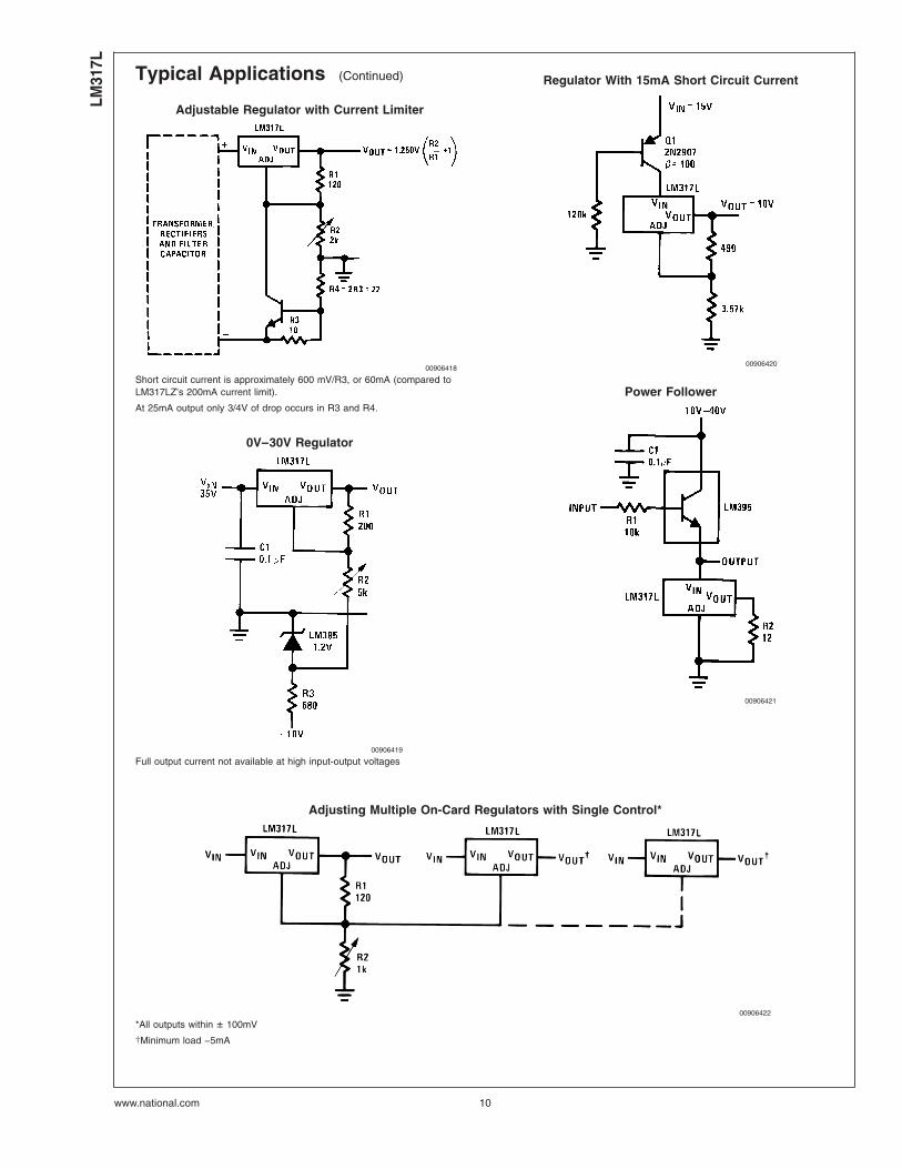
Adjustable Regulator with Current Limiter
00906418
Short circuit current is approximately 600 mV/R3, or 60mA (compared toLM317LZ’s 200mA current limit).
At 25mA output only 3/4V of drop occurs in R3 and R4.
0V–30V Regulator
00906419
Full output current not available at high input-output voltages
Regulator With 15mA Short Circuit Current
00906420
Power Follower
00906421
Adjusting Multiple On-Card Regulators with Single Control*
00906422
*All outputs within ± 100mV
†Minimum load −5mA
LM31
7L
www.national.com 10

Typical Applications (Continued)
100mA Current Regulator
00906423
1.2V–12V Regulator with Minimum Program Current
00906424
*Minimum load current ≈ 2 mA
50mA Constant Current BatteryCharger for Nickel-Cadmium
Batteries
00906425
5V Logic Regulator with Electronic Shutdown*
00906426
*Minimum output ≈ 1.2V
Current Limited 6V Charger
00906427
*Sets peak current, IPEAK = 0.6V/R1
**1000µF is recommended to filter out any input transients.
LM317L
www.national.com11

Typical Applications (Continued)
Short Circuit Protected 80V Supply
00906428
Basic High Voltage Regulator
00906429
Q1, Q2: NSD134 or similar
C1, C2: 1µF, 200V mylar**
*Heat sink
LM31
7L
www.national.com 12

Typical Applications (Continued)
Precision High Voltage Regulator
00906430
Q1, Q2: NSD134 or similar
C1, C2: 1µF, 200V mylar**
*Heat sink
**Mylar is a registered trademark of DuPont Co.
Tracking Regulator
00906431
A1 = LM301A, LM307, or LF13741 only
R1, R2 = matched resistors with good TC tracking
Regulator With Trimmable Output Voltage
00906432
Trim Procedure:
— If VOUT is 23.08V or higher, cut out R3 (if lower, don’t cut it out).
— Then if VOUT is 22.47V or higher, cut out R4 (if lower, don’t).
— Then if VOUT is 22.16V or higher, cut out R5 (if lower, don’t).
This will trim the output to well within ±1% of 22.00 VDC, without any ofthe expense or uncertainty of a trim pot (see LB-46). Of course, thistechnique can be used at any output voltage level.
LM317L
www.national.com13

Typical Applications (Continued)
Precision Reference with Short-Circuit Proof Output
00906433
*R1–R4 from thin-film network,
Beckman 694-3-R2K-D or similar
1.2V-25 Adjustable Regulator
00906401
Full output current not available at high input-output voltages
†Optional — improves transient response
*Needed if device is more than 6 inches from filter capacitors
Fully Protected (Bulletproof)Lamp Driver
00906402
Lamp Flasher
00906403
Output rate — 4 flashes per second at 10% duty cycle
LM31
7L
www.national.com 14

Physical Dimensions inches (millimeters) unless otherwise noted
SO-8 Molded PackageNS Package Number M08A
TO-92 Plastic Package (Z)NS Package Number Z03A
LM317L
www.national.com15

Physical Dimensions inches (millimeters) unless otherwise noted (Continued)
NOTE: UNLESS OTHERWISE SPECIFIED.
1. EPOXY COATING
2. 63Sn/37Pb EUTECTIC BUMP.
3. RECOMMEND NON-SOLDER MASK DEFINED LANDING PAD.
4. PIN A1 IS ESTABLISHED BY LOWER LEFT CORNER WITH RESPECT TO TEXT ORIENTATION PINS ARE NUMBERED COUNTERCLOCKWISE.
5. XXX IN DRAWING NUMBER REPRESENTS PACKAGE SIZE VARIATION WHERE X1 IS PACKAGE WIDTH, X2 IS PACKAGE LENGTH AND X3 ISPACKAGE HEIGHT.
6. REFERENCE JEDEC REGISTRATION MO-211, VARIATION BC.
6-Bump micro SMDNS Package Number BPA06HPB
X1 = 0.955 X2 = 1.615 X3 =0.850
National does not assume any responsibility for use of any circuitry described, no circuit patent licenses are implied and National reservesthe right at any time without notice to change said circuitry and specifications.
For the most current product information visit us at www.national.com.
LIFE SUPPORT POLICY
NATIONAL’S PRODUCTS ARE NOT AUTHORIZED FOR USE AS CRITICAL COMPONENTS IN LIFE SUPPORT DEVICES OR SYSTEMSWITHOUT THE EXPRESS WRITTEN APPROVAL OF THE PRESIDENT AND GENERAL COUNSEL OF NATIONAL SEMICONDUCTORCORPORATION. As used herein:
1. Life support devices or systems are devices or systemswhich, (a) are intended for surgical implant into the body, or(b) support or sustain life, and whose failure to perform whenproperly used in accordance with instructions for useprovided in the labeling, can be reasonably expected to resultin a significant injury to the user.
2. A critical component is any component of a life supportdevice or system whose failure to perform can be reasonablyexpected to cause the failure of the life support device orsystem, or to affect its safety or effectiveness.
BANNED SUBSTANCE COMPLIANCE
National Semiconductor manufactures products and uses packing materials that meet the provisions of the Customer ProductsStewardship Specification (CSP-9-111C2) and the Banned Substances and Materials of Interest Specification (CSP-9-111S2) and containno ‘‘Banned Substances’’ as defined in CSP-9-111S2.
Leadfree products are RoHS compliant.
National SemiconductorAmericas CustomerSupport CenterEmail: [email protected]: 1-800-272-9959
National SemiconductorEurope Customer Support Center
Fax: +49 (0) 180-530 85 86Email: [email protected]
Deutsch Tel: +49 (0) 69 9508 6208English Tel: +44 (0) 870 24 0 2171Français Tel: +33 (0) 1 41 91 8790
National SemiconductorAsia Pacific CustomerSupport CenterEmail: [email protected]
National SemiconductorJapan Customer Support CenterFax: 81-3-5639-7507Email: [email protected]: 81-3-5639-7560
www.national.com
LM31
7L3-
Term
inal
Adj
usta
ble
Reg
ulat
or