Embed Size (px)
Citation preview
LM3519High Frequency Boost White LED Driver withHigh-Speed PWM Brightness ControlGeneral DescriptionThe LM3519 drives up to 4 white LEDs with constant currentto provide LCD backlighting in handheld devices. The LEDcurrent is internally set to 20mA. The series connectionallows the LED current to be identical for uniform brightnessand minimizes the number of traces to the LEDs. Brightnesscontrol is achieved by applying a PWM signal on enable withfrequencies up to 30kHz.
The LM3519 features a proprietary PFM regulation architec-ture with switching frequencies between 2MHz to 8MHz,minimizing inductor size.
Over-voltage protection circuitry and high frequency opera-tion permit the use of low-cost small output capacitors. Dur-ing shutdown, the output is disconnected from the input inorder to avoid leakage current path through the LEDs toground.
The LM3519 is available in a tiny 6-pin SOT23 package.
Featuresn Drives 2 to 4 LEDs at 20mAn Up to 30kHz PWM Dimming Control Capabilityn >80% Peak Efficiencyn Up to 8MHz Switching Frequencyn Small External Components: 1µH - 3.3µH(typ.2.2µH)
Inductor and 1µF Output Capacitorn True Shutdown Isolationn Over-Voltage Protectionn Wide Input Voltage Range: 2.7V to 5.5Vn Small Footprint SOT23-6 Package
Applicationsn LCD, White LED Backlighting on Mobile Phonesn Digital Still Cameras and PDAsn General Purpose LED Lighting in Handheld Devices
Typical Application
20160201
FIGURE 1. Typical Application Circuit
September 2005LM
3519H
ighFrequency
Boost
White
LED
Driver
with
High-S
peedP
WM
Brightness
Control
© 2005 National Semiconductor Corporation DS201602 www.national.com
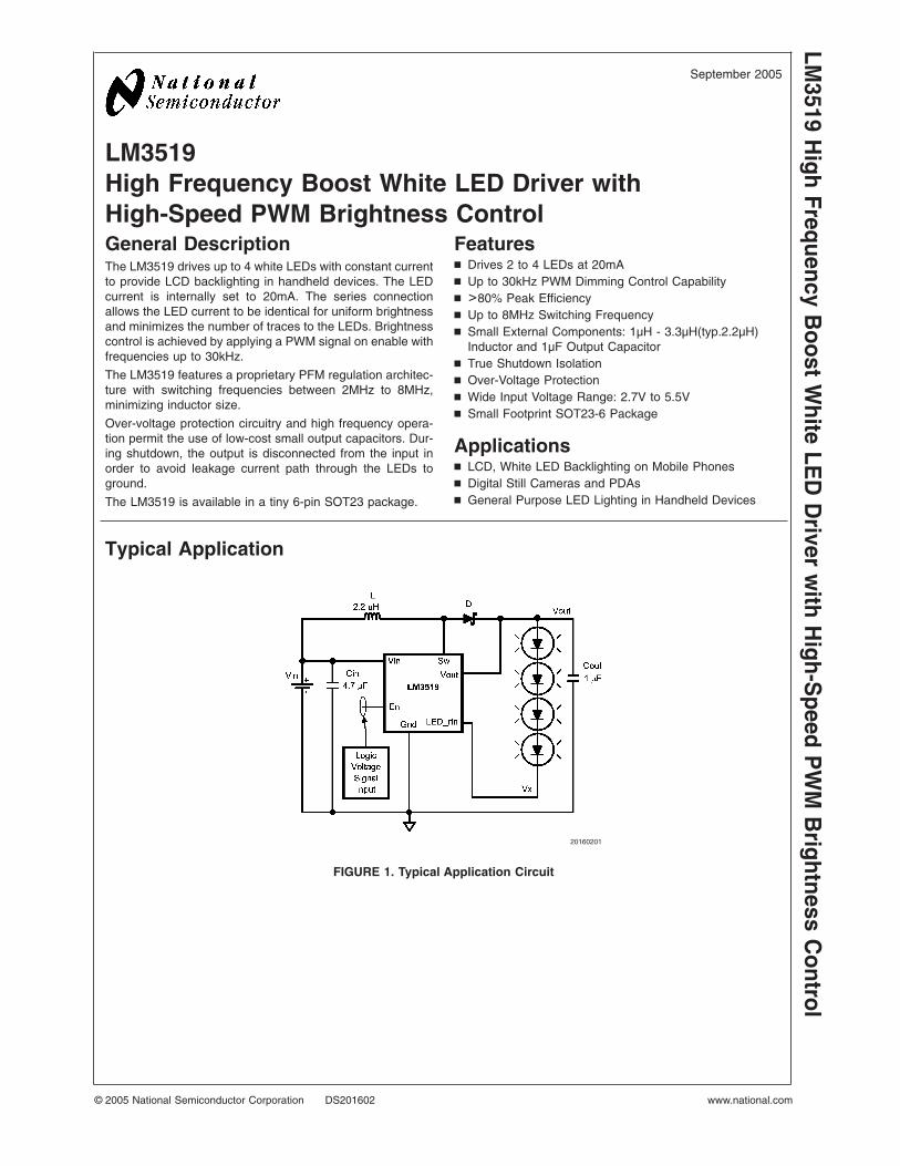
Connection Diagram6-Lead SOT23 Package
20160202
Top View
Pin Descriptions
Pin # Name Description
1 En Device Enable Connection
2 Gnd Ground Connection
3 VOUT Output Voltage Connection
4 LED_rtn White LED Current Sensing Input Connection
5 SW Drain Connection of the Internal Power Field Effect Transistor (FET) Switch
6 VIN Input or Supply Voltage Connection
Ordering Information
CurrentOption Order Number
PackageMarking Supplied As
20 mALM3519MK-20 D52B 1000 Units, Tape-and-Reel
LM3519MKX-20 D52B 3000 Units, Tape-and-Reel
LM35
19
www.national.com 2
Absolute Maximum Ratings (Note 1)
If Military/Aerospace specified devices are required,please contact the National Semiconductor Sales Office/Distributors for availability and specifications.
VIN , En, & LED_rtn Pin −0.3V to +6.5V
VOUT , Sw Pin −0.3V to +21V
Maximum Junction Temperature(TJ-MAX) +150˚C
Storage Temperature Range −65˚C to +150˚C
ESD Rating (Note 2)Human Body Model:Machine Model:
2kV200V
Operating RatingsJunction Temperature (TJ) Range −40˚C to +125˚C
Ambient Temperature (TA) Range −40˚C to +85˚C
Input Voltage Range 2.7V to 5.5V
Thermal Properties (Note 4)
Junction-to-Ambient Thermal Resistance (θJA) 220˚C/W
Electrical Characteristics (Note 5) Limits in standard typeface are for TJ = +25˚C. Limits in bold typefaceapply over the full operating junction temperature range (−40˚C ≤ TJ ≤ +125˚C). VIN = 3.6V, unless otherwise stated.
Symbol Parameter Conditions Min Typ Max Units
IQ Supply Current
Shutdown: VEN = 0V 0.1
µANot Switching: VEN = 1.8V 360 500
Switching: VEN = 1.8V,LED_rtn current = 30mA
550 900
ILED(TOL) LED CurrentTolerance/Variation
VIN = 3.6V, 2.2µH,4LEDs
–10 5.5 10 %
OVP Over-Voltage ProtectionThreshold
OVP ONOVP OFF
1817.8
18.918.6
2019.8
V
ILIM Switch Current Limit L = 2.2µH 750 mA
RDS(ON) Power NMOS Switch ONResistance
455 mΩ
ILEAKAGE Switch Leakage VSW = 3.6V, VEN = 0V 0.1 2 µA
RLED_rtn(ON) LED_rtn NMOS SwitchON Resistance
8.0 Ω
FS Switching Frequency ILED = 20 mA , L = 1µH4LEDs
5.4 MHz
IEN Enable Pin Bias Current(Note 3)
VEN = 0VVEN = 1.8V
0.11.1 2
µA
En Enable Threshold Device OnDevice Off
0.90.3
V
Note 1: Absolute maximum ratings indicate limits beyond which damage to the device may occur. Operating Ratings are conditions under which operation of thedevice is guaranteed. Operating Ratings do not imply guaranteed limits. For guaranteed performance limits and associated test conditions, see the ElectricalCharacteristics table.
Note 2: The human body model is a 100pF capacitor discharged through a 1.5kΩ resistor into each pin. The machine model is a 200pF capacitor discharged directlyinto each pin.
Note 3: Current flows into the pin.
Note 4: The maximum allowable power dissipation is a function of the maximum junction temperature, TJ(MAX), the junction-to-ambient thermal resistance, θJA,and the ambient temperature, TA. See Thermal Properties for the thermal resistance. The maximum allowable power dissipation at any ambient temperature iscalculated using: PD(MAX) = (TJ(MAX) – TA)/θJA. Exceeding the maximum allowable power dissipation will cause excessive die temperature.
Note 5: Min and max limits are guaranteed by design, test, or statistical analysis. Typical numbers are not guaranteed, but do represent the most likely norm.
LM3519
www.national.com3
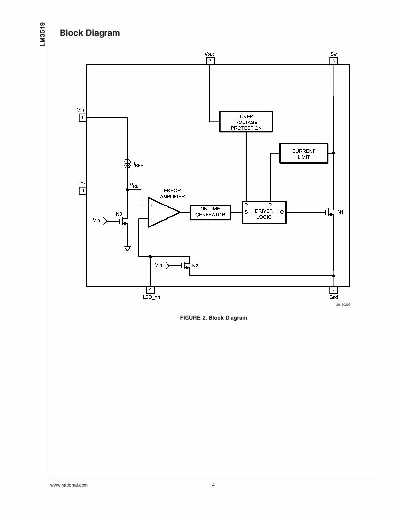
Block Diagram
20160203
FIGURE 2. Block Diagram
LM35
19
www.national.com 4
Circuit DescriptionThe LM3519 is a step-up converter for white LED applica-tions that uses a unique and proprietary pulse frequencymodulation (PFM) architecture to optimize high efficiency athigh frequency operation. Unlike most PFM architectureimplementations, the LM3519’s unique architectural imple-mentation results in non-pulse skipping variable frequencyoperation. The regulator is forced to operate at the edge ofContinous Conduction Mode (CCM). The error amplifier willset the end of the on-time (IPEAK of inductor) based on theload (LEDs) current. During this operation, the inductor cur-rent ramps up and reaches a peak current at end of theon-time. At this point, the internal power switch is turned offuntil the inductor current reaches zero, and the cycle repeatsagain. The switching frequency is set based on the charge(on-time) and discharge(off-time) of the inductor current. Thefrequency can range between 2MHz to 8MHz over the op-erating input range.
The LM3519 operation can be best understood through anexamination of the block diagram in Figure 2. When LED
current is out of regulation, the LED_rtn voltage falls belowor rises above the internal reference voltage (VREF). Theerror amplifier will output a signal to increase or decrease theproper on-time duration of N1 power FET. This correctionallows the inductor’s stored energy to increase or decreaseto a sufficient level that when transferred to the load will bringthe LED_rtn current back into regulation.
During steady-state operation for a typical switching cycle,the oscillator sets the driver logic and turns on N1 powerdevice. N1 conducts current through the inductor and re-verse biases the external diode. The LED current is suppliedby the output capacitor when N1 is conducting. Once N1on-time period is concluded, the internal power device isturned off and the external diode is forward baised. Theinductor current then flows through the diode to the LED loadto replenish the output capacitor and keep the LED currentregulated at the trimmed target.
LM3519
www.national.com5
Typical Performance Characteristics (See Typical Application Circuit : VIN = 3.6V, CIN = 4.7µF andCOUT = 1µF, L = 2.2µH and 4 LEDs. TA = +25˚C, unless otherwise stated.)
Efficiency vs VIN Efficiency vs VIN
2016025120160231
Efficiency vs VIN Efficiency vs VIN
20160232 20160233
IOUT_ACCURACY vs VIN IOUT_ACCURACY vs VIN
2016024920160250
LM35
19
www.national.com 6
Typical Performance Characteristics (See Typical Application Circuit : VIN = 3.6V, CIN = 4.7µF andCOUT = 1µF, L = 2.2µH and 4 LEDs. TA = +25˚C, unless otherwise stated.) (Continued)
IOUT vs VIN IOUT vs VIN
20160234 20160235
IOUT vs VIN
IOUT vs PWM Duty Cycle(VIN = 3.6V, L = 2.2µH)
2016025320160260
IOUT vs PWM Duty Cycle(VIN= 3.6V, L = 2.2µH)
IOUT vs PWM Duty Cycle(VIN = 3.6V, L = 1µH)
20160261 20160259
LM3519
www.national.com7
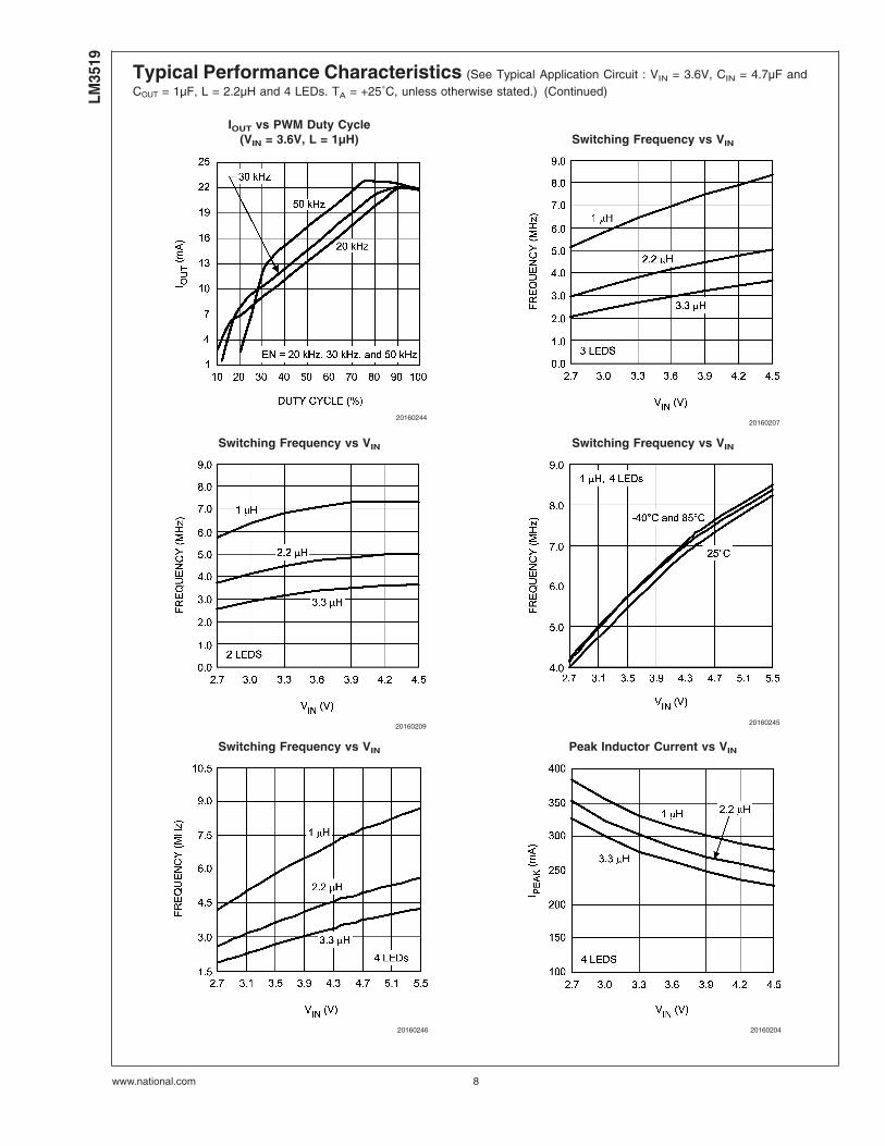
Typical Performance Characteristics (See Typical Application Circuit : VIN = 3.6V, CIN = 4.7µF andCOUT = 1µF, L = 2.2µH and 4 LEDs. TA = +25˚C, unless otherwise stated.) (Continued)
IOUT vs PWM Duty Cycle(VIN = 3.6V, L = 1µH) Switching Frequency vs VIN
2016024420160207
Switching Frequency vs VIN Switching Frequency vs VIN
20160209 20160245
Switching Frequency vs VIN Peak Inductor Current vs VIN
20160246 20160204
LM35
19
www.national.com 8
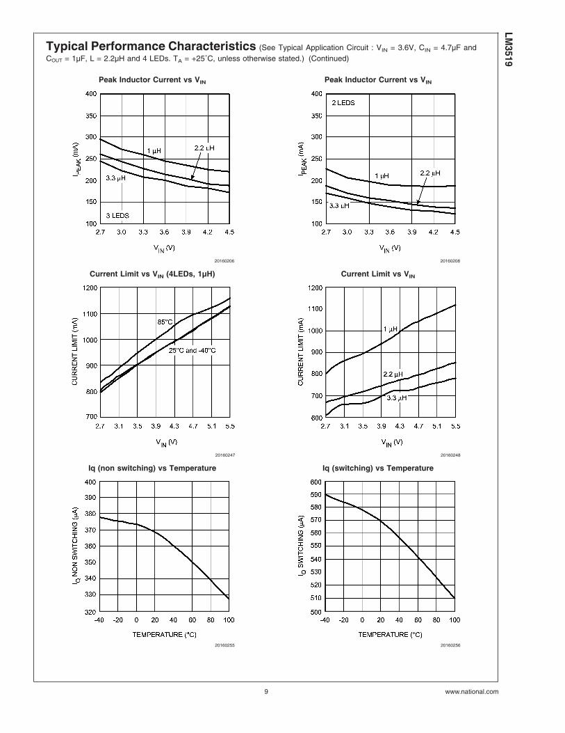
Typical Performance Characteristics (See Typical Application Circuit : VIN = 3.6V, CIN = 4.7µF andCOUT = 1µF, L = 2.2µH and 4 LEDs. TA = +25˚C, unless otherwise stated.) (Continued)
Peak Inductor Current vs VIN Peak Inductor Current vs VIN
20160206 20160208
Current Limit vs VIN (4LEDs, 1µH) Current Limit vs VIN
20160247 20160248
Iq (non switching) vs Temperature Iq (switching) vs Temperature
20160255 20160256
LM3519
www.national.com9
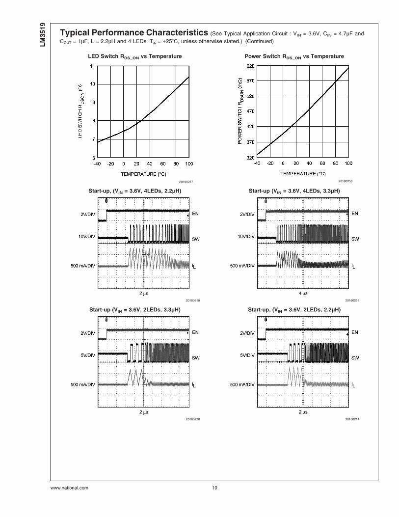
Typical Performance Characteristics (See Typical Application Circuit : VIN = 3.6V, CIN = 4.7µF andCOUT = 1µF, L = 2.2µH and 4 LEDs. TA = +25˚C, unless otherwise stated.) (Continued)
LED Switch RDS_ON vs Temperature Power Switch RDS_ON vs Temperature
20160257 20160258
Start-up, (VIN = 3.6V, 4LEDs, 2.2µH) Start-up (VIN = 3.6V, 4LEDs, 3.3µH)
20160210 20160219
Start-up (VIN = 3.6V, 2LEDs, 3.3µH) Start-up, (VIN = 3.6V, 2LEDs, 2.2µH)
20160220 20160211
LM35
19
www.national.com 10
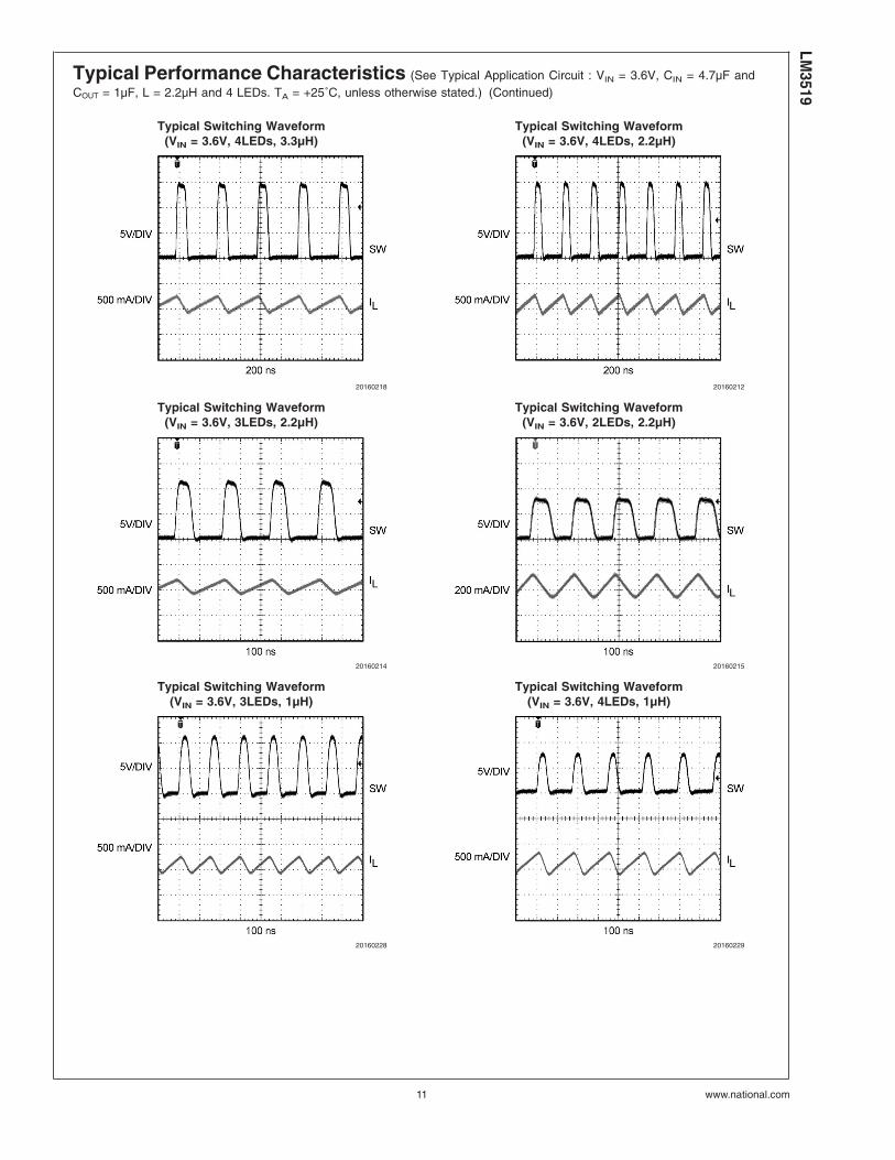
Typical Performance Characteristics (See Typical Application Circuit : VIN = 3.6V, CIN = 4.7µF andCOUT = 1µF, L = 2.2µH and 4 LEDs. TA = +25˚C, unless otherwise stated.) (Continued)
Typical Switching Waveform(VIN = 3.6V, 4LEDs, 3.3µH)
Typical Switching Waveform(VIN = 3.6V, 4LEDs, 2.2µH)
20160218 20160212
Typical Switching Waveform(VIN = 3.6V, 3LEDs, 2.2µH)
Typical Switching Waveform(VIN = 3.6V, 2LEDs, 2.2µH)
20160214 20160215
Typical Switching Waveform(VIN = 3.6V, 3LEDs, 1µH)
Typical Switching Waveform(VIN = 3.6V, 4LEDs, 1µH)
20160228 20160229
LM3519
www.national.com11
Application Information
CAPACITOR SELECTION
To minimize output and input voltage ripple, low equivalentseries resistance (ESR) ceramic capacitors are the bestchoice to use for the input and output filters. For most displayapplications, a 4.7µF capacitor is recommended for CIN and1µF for COUT .
Larger output capacitors can be used to reduce ripple volt-age. To guarantee good performance, a minimum of 0.47µFCOUT is required to trade off for large ripple voltage. Caremust be taken to account for the true capacitance of amultilayer ceramic capacitor. Smaller case size capacitorstypically have less capacitance for a given bias voltage ascompared to a larger case size capacitor with the same biasvoltage. Please confirm with capacitor manufacturer databefore selecting the capacitor.
Some recommended capacitor manufacturers include butare not limited to:
Manufacturer Description Case Size
AVX06033D105MAT-25V 0603
06036D475MAT-6.3V 0603
TDK C2012X5R1A475M-10V 0805
Taiyo Yuden TMK212BJ105KG-J 0805
EM212BJ475MG-16V 0805
muRata GRM40-034B105K25 0805
GRM39X5R475K6.3 0603
INDUCTOR SELECTION
In order to maintain sufficient inductance, the saturationcurrent rating of the inductor used with the LM3519 shouldbe higher than the peak inductor current in the target appli-cation. Inductors with low DCR values have less power lossand higher efficiency. Larger inductor values such as 2.2µHand 3.3µH can be used to optimize efficiency, frequency andpeak current. If 1µH is used, the peak inductor current,frequency will be higher and the efficiency will be lower. Notethat the switching frequency ranges will be higher at lowerinductance. Typical frequency range is between 4 to 8MHzfor 1µH, 2 to 5MHz for 2.2µH and 2 to 4MHz for 3.3µH overthe input range. Below is a sample list of low profile induc-tors.
Some recommended inductor manufacturers include butare not limited to:
Manufacturer L Case Size ISAT
CoilCraft:DO3314-102
1µH
3.3x3.3x1.4mm
2.1A
DO3314-222 2.2µH 1.6A
DO3314-332 3.3µH 1.4A
Coilcraft:LPO3310-102ML
1µH
3.3x3.3x1.0 mm
1.6A
LPO3310-222ML 2.2µH 1.1A
LPO3310-332ML 3.3µH 0.95A
Cooper:SD31121R0
1µH
3.1x3.1x1.4 mm
2.07A
SD3114-2R2 2.2µH 1.48A
SD3114-3R3 3.3uH 1.15A
Taiyo Yuden:NR3015T1R0N
1µH
3.0x3.0x1.5 mm
2.1A
NR3015T2R2M 2.2µH 1.48A
NR3015T3R3M 3.3µH 1.21A
DIODE SELECTION
Diodes with low forward voltage ratings (VF) and low junctioncapacitance magnitudes (CJ or CT or CD) are conducive tohigh efficiency. The chosen diode must have a reversebreakdown voltage rating (VR and/or VRRM) that is largerthan the output voltage. The following criteria should befollowed when choosing a diode:
1. VR (Diode Blocking Voltage Range) and VRRM (DiodePeak Repetitive Reverse Voltage Rating) > VOUT (Out-put Voltage)
2. IF or IO (Diode Average Forward Current Rating) ≥ ILOAD
(Load Current)
3. IFRM (Diode Peak Repetitive Forward Current Rating) ≥ILpeak (Peak Inductor Current)
Some recommended diode manufacturers include but arenot limited to:
Maufacturer Description
Vishay SS12(1A/20V)
SS14(1A/40V)
SS16(1A/60V)
Central Semiconductor CMSH1- 40M(1A/40V)
ONSemi MBRS1540T3(1.5A/40V)
PWM DIMMING
The LED current is set internally by the LM3519 to 20mA(typical); dimming control may be realized by applying apulse width modulated(PWM) signal to the En pin. For ex-ample, a 50% duty cycle waveform will produce an averagecurrent of 10mA. A control signal frequency between 17kHzand 30kHz is suitable for dimming.
Although the LM3519 is capable of operation outside thisfrequency range, it is not recommended to operate below17kHz for the following reasons: 1) frequency below 100Hzis likely to cause visible flicker in the light emitted by the LEDstring. 2) frequency below 17kHz may induce audible noisedue to combinations of some capacitance/PCB. A PWMfrequency above 30kHz is possible but the current linearityvs duty cycle will be affected.
If it is not possible to operate the dimming control above17kHz, audible noise emission may be minimized by usingcapacitors with low susceptibility to piezoelectric inducedstresses, such as poly film designs. Minimum audible noiseis most likely to occur when the PWM frequency is less than2kHz. It is recommended that any application using a PWMcontrol signal below 17kHz be thoroughly evaluated for un-desirable audible or visible noise.
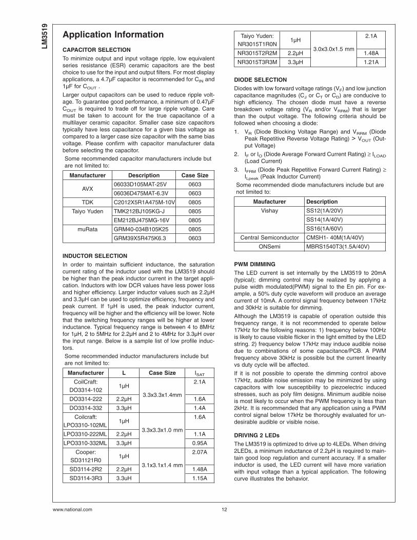
DRIVING 2 LEDs
The LM3519 is optimized to drive up to 4LEDs. When driving2LEDs, a minimum inductance of 2.2µH is required to main-tain good loop regulation and current accuracy. If a smallerinductor is used, the LED current will have more variationwith input voltage than a typical application. The followingcurve illustrates the behavior.
LM35
19
www.national.com 12
Application Information (Continued)
IOUT vs VIN
20160239
LAYOUT GUIDELINES
The input capacitor, CIN, must be placed close to theLM3519. Placing CIN close to the device will reduce themetal trace resistance effect on input voltage ripple. Metaltrace connections for the COUT capacitor can increase theeffective series resistance, which affects output voltageripple and efficiency. Trace connections to the inductorshould be short and wide to reduce power dissipation, in-crease overall efficiency and reduce EMI radiation. The di-ode, like the inductor, should have trace connections that areshort and wide to reduce power dissipation and increaseoverall efficiency. For more details regarding layout guide-lines for switching regulators, refer to Applications Note AN-1149.
LM3519
www.national.com13
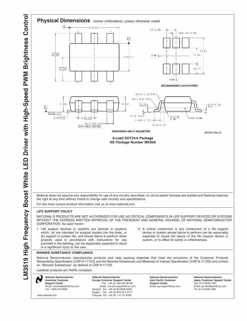
Physical Dimensions inches (millimeters) unless otherwise noted
6-Lead SOT23-6 PackageNS Package Number MK06A
National does not assume any responsibility for use of any circuitry described, no circuit patent licenses are implied and National reservesthe right at any time without notice to change said circuitry and specifications.
For the most current product information visit us at www.national.com.
LIFE SUPPORT POLICY
NATIONAL’S PRODUCTS ARE NOT AUTHORIZED FOR USE AS CRITICAL COMPONENTS IN LIFE SUPPORT DEVICES OR SYSTEMSWITHOUT THE EXPRESS WRITTEN APPROVAL OF THE PRESIDENT AND GENERAL COUNSEL OF NATIONAL SEMICONDUCTORCORPORATION. As used herein:
1. Life support devices or systems are devices or systemswhich, (a) are intended for surgical implant into the body, or(b) support or sustain life, and whose failure to perform whenproperly used in accordance with instructions for useprovided in the labeling, can be reasonably expected to resultin a significant injury to the user.
2. A critical component is any component of a life supportdevice or system whose failure to perform can be reasonablyexpected to cause the failure of the life support device orsystem, or to affect its safety or effectiveness.
BANNED SUBSTANCE COMPLIANCE
National Semiconductor manufactures products and uses packing materials that meet the provisions of the Customer ProductsStewardship Specification (CSP-9-111C2) and the Banned Substances and Materials of Interest Specification (CSP-9-111S2) and containno ‘‘Banned Substances’’ as defined in CSP-9-111S2.
Leadfree products are RoHS compliant.
National SemiconductorAmericas CustomerSupport CenterEmail: [email protected]: 1-800-272-9959
National SemiconductorEurope Customer Support Center
Fax: +49 (0) 180-530 85 86Email: [email protected]
Deutsch Tel: +49 (0) 69 9508 6208English Tel: +44 (0) 870 24 0 2171Français Tel: +33 (0) 1 41 91 8790
National SemiconductorAsia Pacific CustomerSupport CenterEmail: [email protected]
National SemiconductorJapan Customer Support CenterFax: 81-3-5639-7507Email: [email protected]: 81-3-5639-7560
www.national.com
LM35
19H
igh
Freq
uenc
yB
oost
Whi
teLE
DD
rive
rw
ithH
igh-
Spe
edP
WM
Bri
ghtn
ess
Con
trol


![CD-0875[1] Copy](https://img.pdfslide.net/doc/110x75/55cf92fc550346f57b9ae726/cd-08751-copy.jpg)