Embed Size (px)
Citation preview
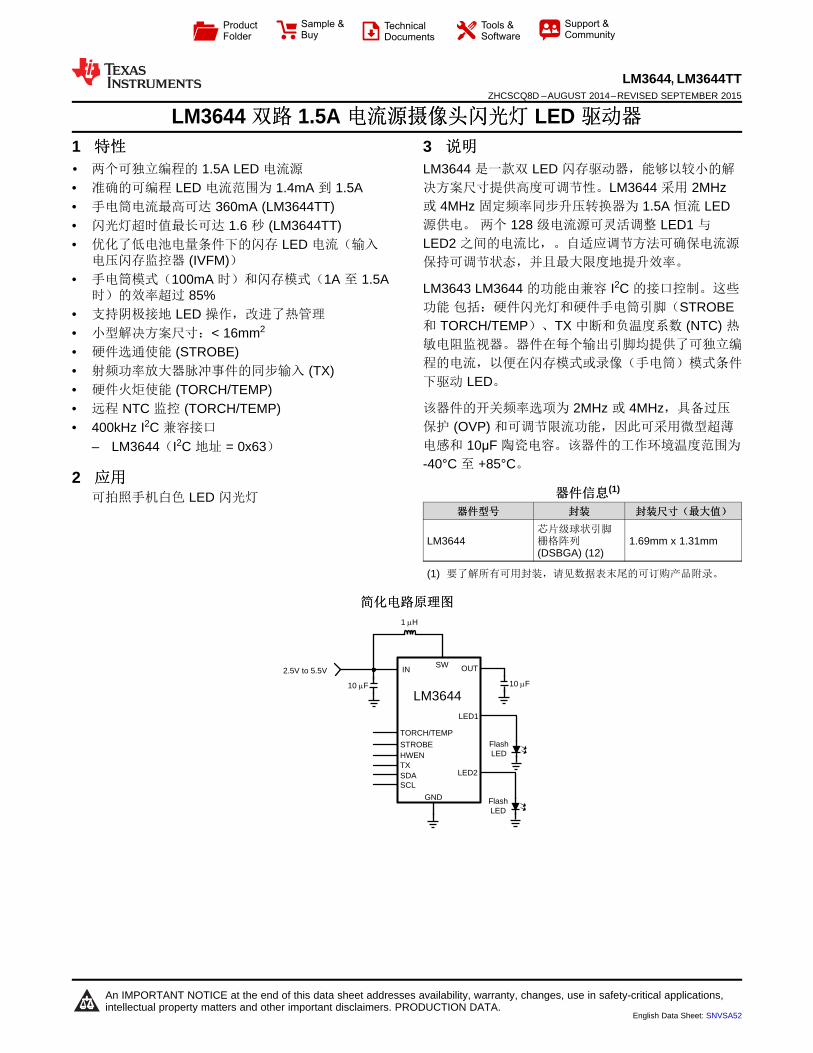
IN OUTSW
HWENTXSDASCL
GND
1 PH
10 PF 10 PF
STROBE
LED1
Flash LED
2.5V to 5.5V
Flash LED
LED2
LM3644
TORCH/TEMP
Product
Folder
Sample &Buy
Technical
Documents
Tools &
Software
Support &Community
An IMPORTANT NOTICE at the end of this data sheet addresses availability, warranty, changes, use in safety-critical applications,intellectual property matters and other important disclaimers. PRODUCTION DATA.
English Data Sheet: SNVSA52
LM3644, LM3644TTZHCSCQ8D –AUGUST 2014–REVISED SEPTEMBER 2015
LM3644 双双路路 1.5A 电电流流源源摄摄像像头头闪闪光光灯灯 LED 驱驱动动器器
1
1 特特性性
1• 两个可独立编程的 1.5A LED 电流源
• 准确的可编程 LED 电流范围为 1.4mA 到 1.5A• 手电筒电流最高可达 360mA (LM3644TT)• 闪光灯超时值最长可达 1.6 秒 (LM3644TT)• 优化了低电池电量条件下的闪存 LED 电流(输入
电压闪存监控器 (IVFM))• 手电筒模式(100mA 时)和闪存模式(1A 至 1.5A
时)的效率超过 85%• 支持阴极接地 LED 操作,改进了热管理
• 小型解决方案尺寸:< 16mm2
• 硬件选通使能 (STROBE)• 射频功率放大器脉冲事件的同步输入 (TX)• 硬件火炬使能 (TORCH/TEMP)• 远程 NTC 监控 (TORCH/TEMP)• 400kHz I2C 兼容接口
– LM3644(I2C 地址 = 0x63)
2 应应用用可拍照手机白色 LED 闪光灯
3 说说明明
LM3644 是一款双 LED 闪存驱动器,能够以较小的解
决方案尺寸提供高度可调节性。LM3644 采用 2MHz或 4MHz 固定频率同步升压转换器为 1.5A 恒流 LED源供电。 两个 128 级电流源可灵活调整 LED1 与
LED2 之间的电流比,。自适应调节方法可确保电流源
保持可调节状态,并且最大限度地提升效率。
LM3643 LM3644 的功能由兼容 I2C 的接口控制。这些
功能 包括:硬件闪光灯和硬件手电筒引脚(STROBE和 TORCH/TEMP)、TX 中断和负温度系数 (NTC) 热敏电阻监视器。器件在每个输出引脚均提供了可独立编
程的电流,以便在闪存模式或录像(手电筒)模式条件
下驱动 LED。
该器件的开关频率选项为 2MHz 或 4MHz,具备过压
保护 (OVP) 和可调节限流功能,因此可采用微型超薄
电感和 10μF 陶瓷电容。该器件的工作环境温度范围为
-40°C 至 +85°C。
器器件件信信息息(1)
器器件件型型号号 封封装装 封封装装尺尺寸寸((最最大大值值))
LM3644芯片级球状引脚栅格阵列(DSBGA) (12)
1.69mm x 1.31mm
(1) 要了解所有可用封装,请见数据表末尾的可订购产品附录。
简简化化电电路路原原理理图图

2
LM3644, LM3644TTZHCSCQ8D –AUGUST 2014–REVISED SEPTEMBER 2015 www.ti.com.cn
Copyright © 2014–2015, Texas Instruments Incorporated
目目录录
1 特特性性.......................................................................... 12 应应用用.......................................................................... 13 说说明明.......................................................................... 14 修修订订历历史史记记录录 ........................................................... 25 Device Comparison Table ..................................... 26 Pin Configuration and Functions ......................... 37 Specifications......................................................... 4
7.1 Absolute Maximum Ratings ...................................... 47.2 ESD Ratings ............................................................ 47.3 Recommended Operating Conditions....................... 47.4 Thermal Information .................................................. 47.5 Electrical Characteristics........................................... 57.6 Timing Requirements ............................................... 67.7 Switching Characteristics .......................................... 67.8 Typical Characteristics .............................................. 6
8 Detailed Description ............................................ 128.1 Overview ................................................................. 128.2 Functional Block Diagram ...................................... 13
8.3 Feature Description ................................................ 138.4 Device Functioning Modes...................................... 158.5 Programming........................................................... 198.6 Register Descriptions .............................................. 21
9 Applications and Implementation ...................... 259.1 Application Information............................................ 259.2 Typical Application ................................................. 25
10 Power Supply Recommendations ..................... 3111 Layout................................................................... 31
11.1 Layout Guidelines ................................................. 3111.2 Layout Example ................................................... 32
12 器器件件和和文文档档支支持持 ..................................................... 3312.1 器件支持 ................................................................ 3312.2 相关文档 ................................................................ 3312.3 商标 ....................................................................... 3312.4 静电放电警告......................................................... 3312.5 术语表 ................................................................... 33
13 机机械械、、封封装装和和可可订订购购信信息息....................................... 33
4 修修订订历历史史记记录录
Changes from Revision C (April 2015) to Revision D Page
• Changed 0x00 to 0x02 - typo ............................................................................................................................................... 21• Changed 0x40 to 0x04 - typo ............................................................................................................................................... 21
Changes from Revision B (November 2014) to Revision C Page
• 已添加 有关 LM3644TT 选项的信息 ....................................................................................................................................... 1• Changed Handling Ratings to ESD Ratings; moved storage temp to Ab Max ..................................................................... 4• Added full Thermal Information information .......................................................................................................................... 4
Changes from Revision A (October 2013) to Revision B Page
• Changed '011' to '000' - typo ................................................................................................................................................ 24
Changes from Original (August 2014) to Revision A Page
• 已更改 标题“具有高侧电流源的 1.5A 同步升压白色 LED 驱动器”至“双路 1.5A 电流源摄像头闪光灯 LED 驱动器” ............... 1• Added Note to beginning of Applications and Implementations section .............................................................................. 25
5 Device Comparison Table
ORDERING PART NUMBER MAXIMUM TORCH CURRENTPER CHANNEL
FLASH TIME-OUT RANGE
LM3644YFFR 179 mA 10 ms to 400 msLM3644TTYFFR 360 mA 40 ms to 1600 ms

Top View
A1 A2
B1 B2 B3
Top View
A3
C2C1 C3
D2 D3D1
Pin A1
3
LM3644, LM3644TTwww.ti.com.cn ZHCSCQ8D –AUGUST 2014–REVISED SEPTEMBER 2015
Copyright © 2014–2015, Texas Instruments Incorporated
6 Pin Configuration and Functions
YFF Package12-Pin DSBGA
Pin FunctionsPIN
TYPE DESCRIPTIONNUMBER NAME
A1 GND Ground Ground
A2 IN Power Input voltage connection. Connect IN to the input supply and bypass to GND with a 10-µF orlarger ceramic capacitor.
A3 SDA I/O Serial data input/output in the I2C Mode on LM3644.B1 SW Power Drain Connection for Internal NMOS and Synchronous PMOS Switches.
B2 STROBE I/O Active high hardware flash enable. Drive STROBE high to turn on Flash pulse. Internal pulldownresistor of 300 kΩ between STROBE and GND.
B3 SCL I/O Serial clock input for LM3644.C1 OUT Power Step-up DC-DC converter output. Connect a 10-µF ceramic capacitor between this pin and GND.
C2 HWEN I/O Active high enable pin. High = Standby, Low = Shutdown/Reset. Internal pulldown resistor of 300kΩ between HWEN and GND.
C3 TORCH/TEMP I/O Torch terminal input or threshold detector for NTC temperature sensing and current scale back.
D1 LED2 Power High-side current source output for flash LED.
D2 TX I/O Configurable dual polarity power amplifier synchronization input. Internal pulldown resistor of 300kΩ between TX and GND.
D3 LED1 Power High-side current source output for flash LED.
4
LM3644, LM3644TTZHCSCQ8D –AUGUST 2014–REVISED SEPTEMBER 2015 www.ti.com.cn
Copyright © 2014–2015, Texas Instruments Incorporated
(1) Stresses beyond those listed under Absolute Maximum Ratings may cause permanent damage to the device. These are stress ratingsonly, which do not imply functional operation of the device at these or any other conditions beyond those indicated under RecommendedOperating Conditions. Exposure to absolute-maximum-rated conditions for extended periods may affect device reliability.
(2) All voltages are with respect to the potential at the GND terminal.(3) Internal thermal shutdown circuitry protects the device from permanent damage. Thermal shutdown engages at TJ = 150°C (typical) and
disengages at TJ = 135°C (typical). Thermal shutdown is ensured by design.(4) For detailed soldering specifications and information, please refer to TI Application Note DSBGA Wafer Level Chip Scale Package
(SNVA009).
7 Specifications
7.1 Absolute Maximum Ratingsover operating free-air temperature range (unless otherwise noted) (1) (2)
MIN MAX UNITIN, SW, OUT, LED1, LED2 −0.3 6 VSDA, SCL, TX, TORCH/TEMP, HWEN, STROBE −0.3 to the lesser of
(VIN+0.3) w/ 6 V max V
Continuous power dissipation (3) Internally limitedJunction temperature (TJ-MAX) 150 °CMaximum lead temperature (soldering) See (4)
Storage temperature, Tstg −65 150 °C
(1) JEDEC document JEP155 states that 500-V HBM allows safe manufacturing with a standard ESD control process.(2) JEDEC document JEP157 states that 250-V CDM allows safe manufacturing with a standard ESD control process.
7.2 ESD RatingsVALUE UNIT
V(ESD)Electrostaticdischarge
Human-body model (HBM), per ANSI/ESDA/JEDEC JS-001 (1) ±2500V
Charged-device model (CDM), per JEDEC specification JESD22-C101 (2) ±1500
(1) Stresses beyond those listed under absolute maximum ratings may cause permanent damage to the device. These are stress ratingsonly, and functional operation of the device at these or any other conditions beyond those indicated under recommended operatingconditions is not implied. Exposure to absolute-maximum-rated conditions for extended periods may affect device reliability.
(2) All voltages are with respect to the potential at the GND terminal.(3) In applications where high power dissipation and/or poor package thermal resistance is present, the maximum ambient temperature may
have to be derated. Maximum ambient temperature (TA-MAX) is dependent on the maximum operating junction temperature (TJ-MAX-OP =125°C), the maximum power dissipation of the device in the application (PD-MAX), and the junction-to-ambient thermal resistance of thepart/package in the application (RθJA), as given by the following equation: TA-MAX = TJ-MAX-OP – (RθJA × PD-MAX).
7.3 Recommended Operating Conditionsover operating free-air temperature range (unless otherwise noted) (1) (2)
MIN MAX UNITVIN 2.5 5.5 VJunction temperature (TJ) −40 125
°CAmbient temperature (TA) (3) −40 85
(1) For more information about traditional and new thermal metrics, see the IC Package Thermal Metrics application report, SPRA953.
7.4 Thermal Information
THERMAL METRIC (1)LM3644
UNITDSBGA12 PINS
RθJA Junction-to-ambient thermal resistance 90.2
°C/WRθJC(top) Junction-to-case (top) thermal resistance 0.5RθJB Junction-to-board thermal resistance 40.0ψJT Junction-to-top characterization parameter 3.0ψJB Junction-to-board characterization parameter 39.2

5
LM3644, LM3644TTwww.ti.com.cn ZHCSCQ8D –AUGUST 2014–REVISED SEPTEMBER 2015
Copyright © 2014–2015, Texas Instruments Incorporated
(1) Minimum (Min) and Maximum (Max) limits are specified by design, test, or statistical analysis. Typical (typ.) numbers are not verified, butdo represent the most likely norm. Unless otherwise specified, conditions for typical specifications are: VIN = 3.6 V and TA = 25°C.
(2) All voltages are with respect to the potential at the GND pin.
7.5 Electrical CharacteristicsTypical limits tested at TA = 25°C. Minimum and maximum limits apply over the full operating ambient temperature range(−40°C ≤ TA ≤ 85°C). Unless otherwise specified, VIN = 3.6 V, HWEN = VIN. (1) (2)
PARAMETER TEST CONDITIONS MIN TYP MAX UNITCURRENT SOURCE SPECIFICATIONS
ILED1/2 Current source accuracy
VOUT = 4 V, flash code = 0x7F = 1.5 Aflash –7% 1.5 7% A
VOUT = 4 V, torch code = 0x3F = 89.3 mAtorch or –10% 89.3 10% mA
ILED1/2Current source accuracy(LM3644TT)
VOUT = 4 V, torch code = 0x3F = 180 mAtorch -10% 180 -10% mA
VHRLED1 and LED2 current sourceregulation voltage
ILED1/2 = 729 mA Flash 290mV
ILED1/2 = 179 mA Torch 158
VHRLED1 and LED2 current sourceregulation voltage (LM3644TT) ILED1/2 = 360 mA Torch and
Flash 270 mV
VOVPON threshold 4.86 5 5.1
VOFF threshold 4.75 4.88 4.99
STEP-UP DC/DC CONVERTER SPECIFICATIONSRPMOS PMOS switch on-resistance 86 mΩRNMOS NMOS switch on-resistance 65 mΩ
ICL Switch current limitReg 0x07, bit[0] = 0 –12% 1.9 12%
AReg 0x07, bit[0] = 1 –12% 2.8 12%
UVLO Undervoltage lockout threshold Falling VIN –2% 2.5 2% VVTRIP NTC comparator trip threshold Reg 0x09, bits[3:1] = '100' –5% 0.6 5% VINTC NTC current –6% 50 6% µA
VIVFMInput voltage flash monitor tripthreshold Reg 0x02, bits[5:3] = '000' –3% 2.9 3% V
IQ Quiescent supply current Device not switching pass mode 0.3 0.75 mA
ISD Shutdown supply current Device disabled, HWEN = 0 V2.5 V ≤ VIN ≤ 5.5 V 0.1 4 µA
ISB Standby supply current Device disabled, HWEN = 1.8 V2.5 V ≤ VIN ≤ 5.5 V 2.5 10 µA
HWEN, TORCH/TEMP, STROBE, TX VOLTAGE SPECIFICATIONSVIL Input logic low
2.5 V ≤ VIN ≤ 5.5 V0 0.4 V
VIH Input logic high 1.2 VIN VI2C-COMPATIBLE INTERFACE SPECIFICATIONS (SCL, SDA)VIL Input logic low
2.5 V ≤ VIN ≤ 4.2 V0 0.4 V
VIH Input logic high 1.2 VIN VVOL Output logic low ILOAD = 3 mA 400 mV
LED1 Code (dec#)
I LE
D1
(A)
0 16 32 48 64 80 96 112 1280
0.2
0.4
0.6
0.8
1
1.2
1.4
1.6
D001
TA = -40°CTA = +25°CTA = +85°C
LED2 Code (dec#)
I LE
D2
(A)
0 16 32 48 64 80 96 112 1280
0.2
0.4
0.6
0.8
1
1.2
1.4
1.6
D002
TA = -40°CTA = +25°CTA = +85°C
SCL
SDA_IN
SDA_OUT
t5
t1
t4
t3
t2
6
LM3644, LM3644TTZHCSCQ8D –AUGUST 2014–REVISED SEPTEMBER 2015 www.ti.com.cn
Copyright © 2014–2015, Texas Instruments Incorporated
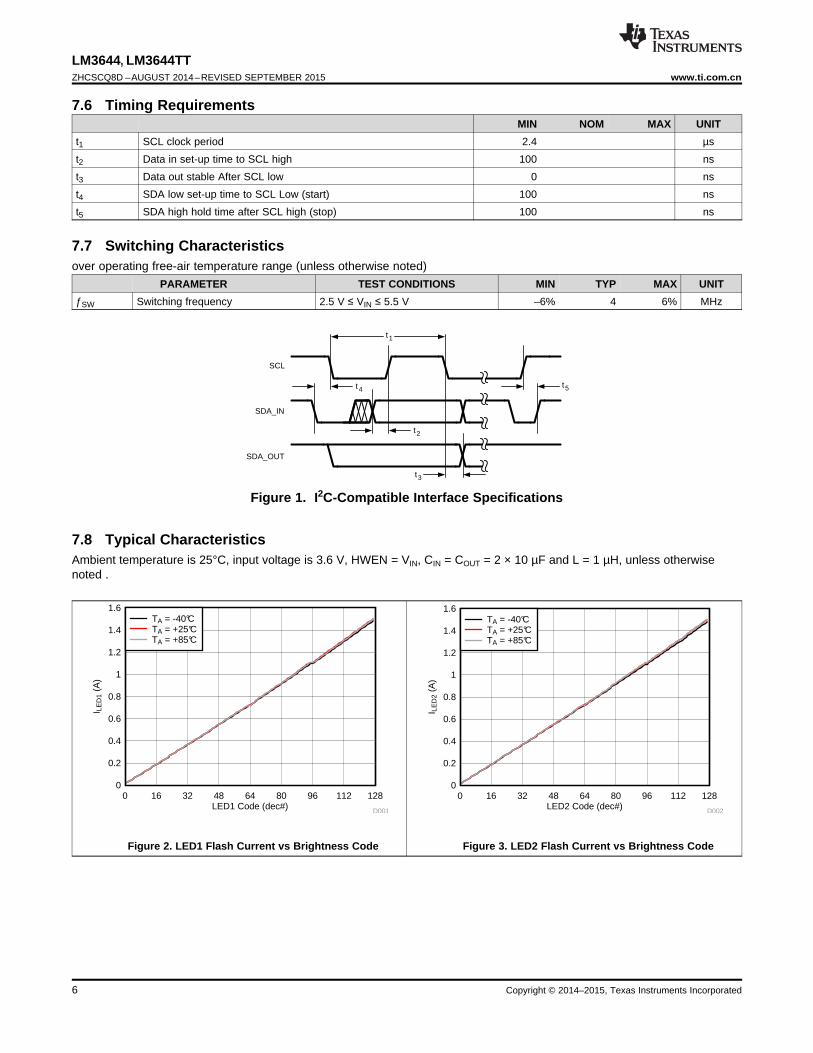
7.6 Timing RequirementsMIN NOM MAX UNIT
t1 SCL clock period 2.4 µst2 Data in set-up time to SCL high 100 nst3 Data out stable After SCL low 0 nst4 SDA low set-up time to SCL Low (start) 100 nst5 SDA high hold time after SCL high (stop) 100 ns
7.7 Switching Characteristicsover operating free-air temperature range (unless otherwise noted)
PARAMETER TEST CONDITIONS MIN TYP MAX UNITƒSW Switching frequency 2.5 V ≤ VIN ≤ 5.5 V –6% 4 6% MHz
Figure 1. I2C-Compatible Interface Specifications
7.8 Typical CharacteristicsAmbient temperature is 25°C, input voltage is 3.6 V, HWEN = VIN, CIN = COUT = 2 × 10 µF and L = 1 µH, unless otherwisenoted .
Figure 2. LED1 Flash Current vs Brightness Code Figure 3. LED2 Flash Current vs Brightness Code

VIN (V)
I LE
D1
(A)
2.5 3 3.5 4 4.5 5 5.50
0.1
0.2
0.3
0.4
0.5
0.6
0.7
0.8
D003
BRC = 0BRC = 7BRC = 15BRC = 23BRC = 31BRC = 39BRC = 47BRC = 55BRC = 63
VIN (V)
I LE
D1
(A)
2.5 3 3.5 4 4.5 5 5.50.7
0.8
0.9
1
1.1
1.2
1.3
1.4
1.5
1.6
D004
BRC = 71BRC = 79BRC = 87BRC = 95BRC = 103BRC = 111BRC = 119BRC = 127
LED1 Code (dec#)
I LE
D1
(A)
0 16 32 48 64 80 96 112 1280
0.04
0.08
0.12
0.16
0.2
0.24
0.28
0.32
0.36
0.4
D040
TA = -40°CTA = +25°CTA = +85°C
LED2 Code (dec#)
I LE
D2
(A)
0 16 32 48 64 80 96 112 1280
0.04
0.08
0.12
0.16
0.2
0.24
0.28
0.32
0.36
0.4
D040D041
TA = -40°CTA = +25°CTA = +85°C
LED1 Code (dec#)
I LE
D1
(A)
0 16 32 48 64 80 96 112 1280
0.02
0.04
0.06
0.08
0.1
0.12
0.14
0.16
0.18
0.2
D015
TA = -40°CTA = +25°CTA = +85°C
LED2 Code (dec#)
I LE
D2
(A)
0 16 32 48 64 80 96 112 1280
0.02
0.04
0.06
0.08
0.1
0.12
0.14
0.16
0.18
0.2
D016
TA = -40°CTA = +25°CTA = +85°C
7
LM3644, LM3644TTwww.ti.com.cn ZHCSCQ8D –AUGUST 2014–REVISED SEPTEMBER 2015
Copyright © 2014–2015, Texas Instruments Incorporated
Typical Characteristics (continued)Ambient temperature is 25°C, input voltage is 3.6 V, HWEN = VIN, CIN = COUT = 2 × 10 µF and L = 1 µH, unless otherwisenoted .
Figure 4. LED1 Torch Current vs Brightness Code Figure 5. LED2 Torch Current vs Brightness Code
LM3644TT
Figure 6. LED1 Torch Current vs Brightness Code
LM3644TT
Figure 7. LED2 Torch Current vs Brightness Code
Figure 8. LED1 Current vs Input Voltage Figure 9. LED1 Current vs Input Voltage

VIN (V)
I LE
D (
A)
2.5 3 3.5 4 4.5 5 5.50.930.940.950.960.970.980.99
11.011.021.031.041.051.061.07
D023
TA = -40qCTA = +25qCTA = +85qC
VIN (V)
I LE
D (
A)
2.5 3 3.5 4 4.5 5 5.50.68
0.69
0.7
0.71
0.72
0.73
0.74
0.75
0.76
0.77
0.78
D024
LED1, TA = -40qCLED2, TA = -40qCLED1, TA = +25qCLED2, TA = +25qCLED1, TA = +85qCLED2, TA = +85qC
VIN (V)
I LE
D (
A)
2.5 3 3.5 4 4.5 5 5.51.4
1.42
1.44
1.46
1.48
1.5
1.52
1.54
1.56
1.58
1.6
1.62
D022
TA = -40qCTA = +25qCTA = +85qC
VIN (V)
I LE
D (
A)
2.5 3 3.5 4 4.5 5 5.51.4
1.42
1.44
1.46
1.48
1.5
1.52
1.54
1.56
1.58
1.6
D021
TA = -40qCTA = +25qCTA = +85qC
VIN (V)
I LE
D2
(A)
2.5 3 3.5 4 4.5 5 5.50
0.1
0.2
0.3
0.4
0.5
0.6
0.7
0.8
D005
BRC = 0BRC = 7BRC = 15BRC = 23BRC = 31BRC = 39BRC = 47BRC = 55BRC = 63
VIN (V)
I LE
D2
(A)
2.5 3 3.5 4 4.5 5 5.50.7
0.8
0.9
1
1.1
1.2
1.3
1.4
1.5
1.6
D006
BRC = 71BRC = 79BRC = 87BRC = 95BRC = 103BRC = 111BRC = 119BRC = 127
8
LM3644, LM3644TTZHCSCQ8D –AUGUST 2014–REVISED SEPTEMBER 2015 www.ti.com.cn
Copyright © 2014–2015, Texas Instruments Incorporated
Typical Characteristics (continued)Ambient temperature is 25°C, input voltage is 3.6 V, HWEN = VIN, CIN = COUT = 2 × 10 µF and L = 1 µH, unless otherwisenoted .
Figure 10. LED2 Current vs Input Voltage Figure 11. LED2 Current vs Input Voltage
ILED = 1.5 A ƒSW = 2 MHz Flash
Figure 12. LED1/2 Current vs Input Voltage
ILED = 1.5 A ƒSW = 4 MHz Flash
Figure 13. LED1/2 Current vs Input Voltage
ILED = 1 A ƒSW = 2 MHz Flash
Figure 14. LED1/2 Current vs Input Voltage
ILED = 730 mA ƒSW = 2 MHz Flash
Figure 15. LED1 and LED2 Current vs Input Voltage

VIN (V)
I LE
D (
A)
2.5 3 3.5 4 4.5 5 5.50.16
0.17
0.18
0.19
0.2
D027
LED1, TA = -40qCLED2, TA = -40qCLED1, TA = +25qCLED2, TA = +25qCLED1, TA = +85qCLED2, TA = +85qC
VIN (V)
I LE
D (
A)
2.5 3 3.5 4 4.5 5 5.50.32
0.33
0.34
0.35
0.36
0.37
0.38
0.39
0.4
0.41
0.42
0.43
0.44
0.45
D042
LED1, TA = -40qCLED2, TA = -40qCLED1, TA = +25qCLED2, TA = +25qCLED1, TA = +85qCLED2, TA = +85qC
VIN (V)
I LE
D (
A)
2.5 3 3.5 4 4.5 5 5.50.16
0.17
0.18
0.19
0.2
D025
TA = -40qCTA = -+25qCTA = +85qC
VIN (V)
I LE
D (
A)
2.5 3 3.5 4 4.5 5 5.50.16
0.17
0.18
0.19
0.2
D026
TA = -40qCTA = -+25qCTA = +85qC
VIN (V)
I LE
D (
A)
2.5 3 3.5 4 4.5 5 5.50.65
0.6750.7
0.7250.75
0.7750.8
0.8250.85
0.8750.9
0.9250.95
0.9751
1.0251.05
D037
ILED1, +25qCILED2, +25qCILED1, +85qCILED2, +85qCILED1, -40qCILED2, -40qC
VIN (V)
I LE
D (
A)
2.5 3 3.5 4 4.5 5 5.50.65
0.6750.7
0.7250.75
0.7750.8
0.8250.85
0.8750.9
0.9250.95
0.9751
1.0251.05
D038
ILED1, +25qCILED2, +25qCILED1, +85qCILED2, +85qCILED1, -40qCILED2, -40qC
9
LM3644, LM3644TTwww.ti.com.cn ZHCSCQ8D –AUGUST 2014–REVISED SEPTEMBER 2015
Copyright © 2014–2015, Texas Instruments Incorporated
Typical Characteristics (continued)Ambient temperature is 25°C, input voltage is 3.6 V, HWEN = VIN, CIN = COUT = 2 × 10 µF and L = 1 µH, unless otherwisenoted .
ILED = 1 A ƒSW = 2 MHz Flash
Figure 16. LED1 and LED2 Current vs Input Voltage
ILED = 1 A ƒSW = 4 MHz Flash
Figure 17. LED1 and LED2 Current vs Input Voltage
ILED = 179 mA ƒSW = 2 MHz Torch
Figure 18. LED Current vs Input Voltage
ILED = 179 mA ƒSW = 4 MHz Torch
Figure 19. LED Current vs Input Voltage
ILED = 179 mA ƒSW = 2 MHz Torch
Figure 20. LED1 and LED2 Current vs Input Voltage
LM3644TT ƒSW = 2 MHz TorchILED = 360 mA
Figure 21. LED1 and LED2 Current vs Input Voltage

VIN (V)
I CL
(A)
2.5 2.7 2.9 3.1 3.3 3.5 3.7 3.9 4.1 4.31.6
1.641.681.721.761.8
1.841.881.921.96
22.042.082.122.162.2
D011
TA = -40qCTA = +25qCTA = +85qC
VIN (V)
I CL
(A)
2.5 2.7 2.9 3.1 3.3 3.5 3.7 3.9 4.1 4.31.6
1.641.681.721.761.8
1.841.881.921.96
22.042.082.122.162.2
D012
TA = -40qCTA = +25qCTA = +85qC
VIN (V)
I SB (P
A)
2.5 3 3.5 4 4.5 5 5.50
1
2
3
4
5
6
7
D008
TA = -40qCTA = +25qCTA = +85qC
VIN (V)
I SB (P
A)
2.5 3 3.5 4 4.5 5 5.50
1
2
3
4
5
6
7
D010
TA = -40qCTA = +25qCTA = +85qC
VIN (V)
I SD (P
A)
2.5 3 3.5 4 4.5 5 5.50
0.2
0.4
0.6
0.8
1
1.2
D007
TA = -40qCTA = +25qCTA = +85qC
VIN (V)
I SB (P
A)
2.5 3 3.5 4 4.5 5 5.50
0.5
1
1.5
2
2.5
3
D009
TA = -40qCTA = +25qCTA = +85qC
10
LM3644, LM3644TTZHCSCQ8D –AUGUST 2014–REVISED SEPTEMBER 2015 www.ti.com.cn
Copyright © 2014–2015, Texas Instruments Incorporated
Typical Characteristics (continued)Ambient temperature is 25°C, input voltage is 3.6 V, HWEN = VIN, CIN = COUT = 2 × 10 µF and L = 1 µH, unless otherwisenoted .
HWEN = 0 V I2C = 0 V
Figure 22. Shutdown Current vs Input Voltage
HWEN = VIN I2C = VIN
Figure 23. Standby Current vs Input Voltage
HWEN = 1.8 V I2C = 0 V
Figure 24. Standby Current vs Input Voltage
HWEN = 1.8 V I2C = 1.8 V
Figure 25. Standby Current vs Input Voltage
ILED = 1.5 A ƒSW = 2 MHz VLED = 4.5 VICL = 1.9 A
Figure 26. Inductor Current Limit vs Input Voltage
ILED = 1.5 A ƒSW = 4 MHz VLED = 4.5 VICL = 1.9 A
Figure 27. Inductor Current Limit vs Input Voltage

VIN (V)
f SW
(M
Hz)
2.5 2.75 3 3.25 3.5 3.75 4 4.25 4.5 4.75 51.875
1.9
1.925
1.95
1.975
2
2.025
2.05
2.075
2.1
2.125
D017
TA = +25qCTA = +85qCTA = -40qC
VIN (V)
f SW
(M
Hz)
2.5 2.75 3 3.25 3.5 3.75 4 4.25 4.5 4.75 53.75
3.8
3.85
3.9
3.95
4
4.05
4.1
4.15
4.2
4.25
D017D018
TA = +25qCTA = +85qCTA = -40qC
VIN (V)
I CL
(A)
2.5 2.75 3 3.25 3.5 3.75 4 4.25 4.5 4.75 51.4
1.6
1.8
2
2.2
2.4
2.6
2.8
3
D013
TA = -40qCTA = +25qCTA = +85qC
VIN (V)
I CL
(A)
2.5 2.75 3 3.25 3.5 3.75 4 4.25 4.5 4.75 51.4
1.6
1.8
2
2.2
2.4
2.6
2.8
3
D014
TA = -40qCTA = +25qCTA = +85qC
11
LM3644, LM3644TTwww.ti.com.cn ZHCSCQ8D –AUGUST 2014–REVISED SEPTEMBER 2015
Copyright © 2014–2015, Texas Instruments Incorporated
Typical Characteristics (continued)Ambient temperature is 25°C, input voltage is 3.6 V, HWEN = VIN, CIN = COUT = 2 × 10 µF and L = 1 µH, unless otherwisenoted .
ILED = 1.5 A ƒSW = 2 MHz VLED = 4.5 VICL = 2.8 A
Figure 28. Inductor Current Limit vs Input Voltage
ILED = 1.5 A ƒSW = 4 MHz VLED = 4.5 VICL = 2.8 A
Figure 29. Inductor Current Limit vs Input Voltage
Figure 30. 2-MHz Switching Frequency vs Input Voltage Figure 31. 4-MHz Switching Frequency vs Input Voltage

12
LM3644, LM3644TTZHCSCQ8D –AUGUST 2014–REVISED SEPTEMBER 2015 www.ti.com.cn
Copyright © 2014–2015, Texas Instruments Incorporated
8 Detailed Description
8.1 OverviewThe LM3644 is a high-power white LED flash driver capable of delivering up to 1.5 A in either of the two parallelLEDs. The device incorporates a 2-MHz or 4-MHz constant frequency-synchronous current-mode PWM boostconverter and dual high-side current sources to regulate the LED current over the 2.5-V to 5.5-V input voltagerange.
The LM3644 PWM DC-DC boost converter switches and boosts the output to maintain at least VHR across eachof the current sources (LED1/2). This minimum headroom voltage ensures that both current sources remain inregulation. If the input voltage is above the LED voltage + current source headroom voltage the device does notswitch, but turns the PFET on continuously (Pass mode). In Pass mode the difference between (VIN − ILED ×RPMOS) and the voltage across the LED is dropped across the current source.
The LM3644 has three logic inputs including a hardware Flash Enable (STROBE), a hardware Torch Enable(TORCH/TEMP, TORCH = default), and a Flash Interrupt input (TX) designed to interrupt the flash pulse duringhigh battery-current conditions. These logic inputs have internal 300-kΩ (typical) pulldown resistors to GND.
Additional features of the LM3644 include an internal comparator for LED thermal sensing via an external NTCthermistor and an input voltage monitor that can reduce the Flash current during low VIN conditions. It also has aHardware Enable (HWEN) pin that can be used to reset the state of the device and the registers by pulling theHWEN pin to ground.
Control is done via an I2C-compatible interface. This includes adjustment of the Flash and Torch current levels,changing the Flash Timeout Duration, and changing the switch current limit. Additionally, there are flag andstatus bits that indicate flash current time-out, LED overtemperature condition, LED failure (open/short), devicethermal shutdown, TX interrupt, and VIN undervoltage conditions.

+-
VOVP
PWM Control
ThermalShutdown
+150oC
INVREF
I2C
Interface
+
-
+ -
ErrorAmplifier
SlopeCompensation
SDA
SCL
ControlLogic/
Registers
GND
OUT
LED1
TORCH/TEMP
TXSTROBEHWEN
SW
65 m:
86 m:
Over Voltage Comparator
+-
NTC VTRIP
INTC
ILED1
Soft-Start
+-
2/4 MHzOscillator
+-
UVLOInput Voltage Flash Monitor
OUT-VHR
ILED2
LED2FB
SELECT
Current Sense/Current Limit
13
LM3644, LM3644TTwww.ti.com.cn ZHCSCQ8D –AUGUST 2014–REVISED SEPTEMBER 2015
Copyright © 2014–2015, Texas Instruments Incorporated
8.2 Functional Block Diagram
8.3 Feature Description
8.3.1 Flash ModeIn Flash Mode, the LED current sources (LED1/2) provide 128 target current levels from 10.9 mA to 1500 mA.Once the Flash sequence is activated the current source (LED) ramps up to the programmed Flash current bystepping through all current steps until the programmed current is reached. The headroom in the two currentsources can be regulated to provide 10.9 mA to 1.5 A on each of the two output legs. There is an option in theregister settings to keep the two currents in the output leg the same.
When the device is enabled in Flash Mode through the Enable Register, all mode bits in the Enable Register arecleared after a flash time-out event.
VOUT
STROBE
ILED1
ILED2
OFF
PASS
BOOST
M1
,M0
= Z
01[
LE
D1
,LE
D2
= Z
11[
ST
RO
BE
EN
= Z
1[
M1
,M0
= Z
01[
LE
D1
,LE
D2
= Z
10[
ST
RO
BE
EN
= Z
1[
M1
,M0
= Z
00[
LE
D1
,LE
D2
= Z
11[
ST
RO
BE
EN
= Z
1[
14
LM3644, LM3644TTZHCSCQ8D –AUGUST 2014–REVISED SEPTEMBER 2015 www.ti.com.cn
Copyright © 2014–2015, Texas Instruments Incorporated
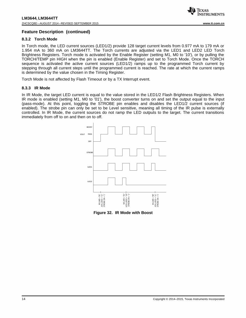
Feature Description (continued)8.3.2 Torch ModeIn Torch mode, the LED current sources (LED1/2) provide 128 target current levels from 0.977 mA to 179 mA or1.954 mA to 360 mA on LM3644TT. The Torch currents are adjusted via the LED1 and LED2 LED TorchBrightness Registers. Torch mode is activated by the Enable Register (setting M1, M0 to '10'), or by pulling theTORCH/TEMP pin HIGH when the pin is enabled (Enable Register) and set to Torch Mode. Once the TORCHsequence is activated the active current sources (LED1/2) ramps up to the programmed Torch current bystepping through all current steps until the programmed current is reached. The rate at which the current rampsis determined by the value chosen in the Timing Register.
Torch Mode is not affected by Flash Timeout or by a TX Interrupt event.
8.3.3 IR ModeIn IR Mode, the target LED current is equal to the value stored in the LED1/2 Flash Brightness Registers. WhenIR mode is enabled (setting M1, M0 to '01'), the boost converter turns on and set the output equal to the input(pass-mode). At this point, toggling the STROBE pin enables and disables the LED1/2 current sources (ifenabled). The strobe pin can only be set to be Level sensitive, meaning all timing of the IR pulse is externallycontrolled. In IR Mode, the current sources do not ramp the LED outputs to the target. The current transitionsimmediately from off to on and then on to off.
Figure 32. IR Mode with Boost

VOUT
STROBE
ILED1
ILED2
TIM
E-O
UT
Sta
rt
TIM
E-O
UT
Sta
rt
TIM
E-O
UT
Sta
rt
TIM
E-O
UT
RE
SE
T
TIM
E-O
UT
RE
SE
T
TIM
E-O
UT
Re
ach
ed
VO
UT
go
es
low
, LE
D1
an
d
2 t
urn
off
Time-Out
Value
M1
,M0
= Z
01[
LED
1,L
ED
2 =
Z1
1[
ST
RO
BE
EN
= Z
1[
M1
,M0
= Z
01[
LE
D1
,LE
D2
= Z
11[
ST
RO
BE
EN
= Z
1[
VOUT
STROBE
ILED1
ILED2
M1
,M0
= Z
01[
LE
D1
,LE
D2
= Z
10[
ST
RO
BE
EN
= Z
1[
M1
,M0
= Z
00[
LE
D1
,LE
D2
= Z
11[
ST
RO
BE
EN
= Z
1[
15
LM3644, LM3644TTwww.ti.com.cn ZHCSCQ8D –AUGUST 2014–REVISED SEPTEMBER 2015
Copyright © 2014–2015, Texas Instruments Incorporated
Feature Description (continued)
Figure 33. IR Mode Pass Only
Figure 34. IR Mode Timeout
8.4 Device Functioning Modes
8.4.1 Start-Up (Enabling The Device)Turn on of the LM3644 Torch and Flash modes can be done through the Enable Register. On start-up, whenVOUT is less than VIN the internal synchronous PFET turns on as a current source and delivers 200 mA (typical)to the output capacitor. During this time the current source (LED) is off. When the voltage across the outputcapacitor reaches 2.2 V (typical) the current source turns on. At turnon the current source steps through eachFLASH or TORCH level until the target LED current is reached. This gives the device a controlled turnon andlimits inrush current from the VIN supply.

16
LM3644, LM3644TTZHCSCQ8D –AUGUST 2014–REVISED SEPTEMBER 2015 www.ti.com.cn
Copyright © 2014–2015, Texas Instruments Incorporated
Device Functioning Modes (continued)8.4.2 Pass ModeThe LM3644 starts up in Pass Mode and stays there until Boost Mode is needed to maintain regulation. If thevoltage difference between VOUT and VLED falls below VHR, the device switches to Boost Mode. In Pass Mode theboost converter does not switch, and the synchronous PFET turns fully on bringing VOUT up to VIN − ILED ×RPMOS. In Pass Mode the inductor current is not limited by the peak current limit.
8.4.3 Power Amplifier Synchronization (TX)The TX pin is a Power Amplifier Synchronization input. This is designed to reduce the flash LED current and thuslimit the battery current during high battery current conditions such as PA transmit events. When the LM3644 isengaged in a Flash event, and the TX pin is pulled high, the LED current is forced into Torch Mode at theprogrammed Torch current setting. If the TX pin is then pulled low before the Flash pulse terminates, the LEDcurrent returns to the previous Flash current level. At the end of the Flash time-out, whether the TX pin is high orlow, the LED current turns off.
8.4.4 Input Voltage Flash Monitor (IVFM)The LM3644 has the ability to adjust the flash current based upon the voltage level present at the IN pin utilizingthe Input Voltage Flash Monitor (IVFM). The adjustable threshold IVFM-D ranges from 2.9 V to 3.6 V in 100-mVsteps, with three different usage modes (Stop and Hold, Adjust Down Only, Adjust Up and Down). The Flags2Register has the IVFM flag bit set when the input voltage crosses the IVFM-D value. Additionally, the IVFM-Dthreshold sets the input voltage boundary that forces the LM3644 to either stop ramping the flash current duringstart-up (Stop and Hold Mode) or to start decreasing the LED current during the flash (Down Adjust Only and Upand Down Adjust). In Adjust Up and Down mode, the IVFM-D value plus the hysteresis voltage threshold set theinput voltage boundary that forces the LM3644 to start ramping the flash current back up towards the target.

IVFM ENABLE
LEVEL STROBE
VIN PROFILE for Stop and Hold Mode
Output Current
Profile in Stop
and Hold Mode
Dotted line shows Output
Current Profile with IVFM
Disabled
Set Target Flash Current
IVFM-D
T-F
ilte
r =
4P
s
VIN PROFILE for Down Mode
IVFM-DHysteresis
SET RAMP FROM
THE RAMP
REGISTER USED
T-F
ilte
r =
4P
s
Output Current
Profile in Down
Mode
VIN PROFILE for Up/ Down Mode
Output Current
Profile in Up and
Down Mode
IVFM-DHysteresis
Hysteresis = 0 V or 50 mV
17
LM3644, LM3644TTwww.ti.com.cn ZHCSCQ8D –AUGUST 2014–REVISED SEPTEMBER 2015
Copyright © 2014–2015, Texas Instruments Incorporated
Device Functioning Modes (continued)
Figure 35. IVFM Modes

VIN
VTRIPControlLogic
NTC Control Block
TEMPINTC
NTC +-
18
LM3644, LM3644TTZHCSCQ8D –AUGUST 2014–REVISED SEPTEMBER 2015 www.ti.com.cn
Copyright © 2014–2015, Texas Instruments Incorporated
Device Functioning Modes (continued)8.4.5 Fault/Protections
8.4.5.1 Fault OperationIf the LM3644 enters a fault condition, the device sets the appropriate flag in the Flags1 and Flags2 Registers(0x0A and 0x0B), and place the device into standby by clearing the Mode Bits ([1],[0]) in the Enable Register.The LM3644 remains in standby until an I2C read of the Flags1 and Flags2 Registers are completed. Uponclearing the flags/faults, the device can be restarted (Flash, Torch, IR, etc.). If the fault is still present, theLM3644 re-enters the fault state and enters standby again.
8.4.5.2 Flash Time-OutThe Flash Time-Out period sets the amount of time that the Flash Current is being sourced from the currentsources (LED1/2). The LM3644 has 16 timeout levels ranging from 10 ms to 400 ms or 40 ms to 1.6 s onLM3644TT (see Timing Configuration Register (0x08) for more detail).
8.4.5.3 Overvoltage Protection (OVP)The output voltage is limited to typically 5 V (see VOVP spec in the Electrical Characteristics). In situations suchas an open LED, the LM3644 raises the output voltage in order to try and keep the LED current at its targetvalue. When VOUT reaches 5 V (typical) the overvoltage comparator trips and turns off the internal NFET. WhenVOUT falls below the “VOVP Off Threshold”, the LM3644 begins switching again. The mode bits are cleared, andthe OVP flag is set, when an OVP condition is present for three rising OVP edges. This prevents momentaryOVP events from forcing the device to shut down.
8.4.5.4 Current LimitThe LM3644 features two selectable inductor current limits that are programmable through the I2C-compatibleinterface. When the inductor current limit is reached, the LM3644 terminates the charging phase of the switchingcycle. Switching resumes at the start of the next switching period. If the overcurrent condition persists, the deviceoperates continuously in current limit.
Since the current limit is sensed in the NMOS switch, there is no mechanism to limit the current when the deviceoperates in Pass Mode (current does not flow through the NMOS in pass mode). In Boost mode or Pass mode ifVOUT falls below 2.3 V, the device stops switching, and the PFET operates as a current source limiting thecurrent to 200 mA. This prevents damage to the LM3644 and excessive current draw from the battery duringoutput short-circuit conditions. The mode bits are not cleared upon a Current Limit event, but a flag is set.
8.4.5.5 NTC Thermistor Input (Torch/Temp)The TORCH/TEMP pin, when set to TEMP mode, serves as a threshold detector and bias source for negativetemperature coefficient (NTC) thermistors. When the voltage at TEMP goes below the programmed threshold,the LM3644 is placed into standby mode. The NTC threshold voltage is adjustable from 200 mV to 900 mV in100-mV steps. The NTC bias current is set to 50 µA. The NTC detection circuitry can be enabled or disabled viathe Enable Register. If enabled, the NTC block turns on and off during the start and stop of a Flash/Torch event.
Additionally, the NTC input looks for an open NTC connection and a shorted NTC connection. If the NTC inputfalls below 100 mV, the NTC short flag is set, and the device is disabled. If the NTC input rises above 2.3 V, theNTC Open flag is set, and the device is disabled. These fault detections can be individually disabled/enabled viathe NTC Open Fault Enable bit and the NTC Short Fault Enable bit.
Figure 36. Temp Detection Diagram

19
LM3644, LM3644TTwww.ti.com.cn ZHCSCQ8D –AUGUST 2014–REVISED SEPTEMBER 2015
Copyright © 2014–2015, Texas Instruments Incorporated
Device Functioning Modes (continued)8.4.5.6 Undervoltage Lockout (UVLO)The LM3644 has an internal comparator that monitors the voltage at IN and forces the LM3644 into standby ifthe input voltage drops to 2.5 V. If the UVLO monitor threshold is tripped, the UVLO flag bit is set in the Flags1Register (0x0A). If the input voltage rises above 2.5 V, the LM3644 is not available for operation until there is anI2C read of the Flags1 Register (0x0A). Upon a read, the Flags1 register is cleared, and normal operation canresume if the input voltage is greater than 2.5 V.
8.4.5.7 Thermal Shutdown (TSD)When the LM3644 die temperature reaches 150°C, the thermal shutdown detection circuit trips, forcing theLM3644 into standby and writing a '1' to the corresponding bit of the Flags1 Register (0x0A) (Thermal Shutdownbit). The LM3644 is only allowed to restart after the Flags1 Register (0x0A) is read, clearing the fault flag. Uponrestart, if the die temperature is still above 150°C, the LM3644 resets the Fault flag and re-enters standby.
8.4.5.8 LED and/or VOUT Short FaultThe LED Fault flags read back a '1' if the device is active in Flash or Torch mode and either active LED outputexperiences a short condition. The Output Short Fault flag reads back a '1' if the device is active in Flash orTorch mode and the boost output experiences a short condition. An LED short condition is determined if thevoltage at LED1 or LED2 goes below 500 mV (typ.) while the device is in Torch or Flash mode. There is adeglitch time of 256 μs before the LED Short flag is valid and a deglitch time of 2.048 ms before the VOUT Shortflag is valid. The LED Short Faults can be reset to '0' by removing power to the LM3644, setting HWEN to '0',setting the SW RESET bit to a '1', or by reading back the Flags1 Register (0x0A on LM3644). The mode bits arecleared upon an LED and/or VOUT short fault.
8.5 Programming
8.5.1 Control Truth Table
MODE1 MODE0 STROBE EN TORCH EN STROBE PIN TORCH PIN ACTION0 0 0 0 X X Standby0 0 0 1 X pos edge Ext Torch0 0 1 0 pos edge X Ext Flash0 0 1 1 0 pos edge Standalone Torch0 0 1 1 pos edge 0 Standalone Flash0 0 1 1 pos edge pos edge Standalone Flash1 0 X X X X Int Torch1 1 X X X X Int Flash0 1 0 X X X IRLED Standby0 1 1 X 0 X IRLED Standby0 1 1 X pos edge X IRLED enabled

SDA
Start Condition Stop Condition
SCLS P
SCL
SDA
data change allowed
data valid
data change allowed
data valid
data change allowed
20
LM3644, LM3644TTZHCSCQ8D –AUGUST 2014–REVISED SEPTEMBER 2015 www.ti.com.cn
Copyright © 2014–2015, Texas Instruments Incorporated
8.5.2 I2C-Compatible Interface
8.5.2.1 Data ValidityThe data on SDA must be stable during the HIGH period of the clock signal (SCL). In other words, the state ofthe data line can only be changed when SCL is LOW.
Figure 37. Data Validity Data
A pullup resistor between the controller's VIO line and SDA must be greater than [(VIO - VOL) / 3 mA] to meet theVOL requirement on SDA. Using a larger pullup resistor results in lower switching current with slower edges, whileusing a smaller pullup results in higher switching currents with faster edges.
8.5.2.2 Start and Stop ConditionsSTART and STOP conditions classify the beginning and the end of the I2C session. A START condition isdefined as the SDA signal transitioning from HIGH to LOW while SCL line is HIGH. A STOP condition is definedas the SDA transitioning from LOW to HIGH while SCL is HIGH. The I2C master always generates START andSTOP conditions. The I2C bus is considered busy after a START condition and free after a STOP condition.During data transmission, the I2C master can generate repeated START conditions. First START and repeatedSTART conditions are equivalent, function-wise.
Figure 38. Start and Stop Conditions
8.5.2.3 Transferring DataEvery byte put on the SDA line must be eight bits long, with the most significant bit (MSB) transferred first. Eachbyte of data has to be followed by an acknowledge bit. The acknowledge related clock pulse is generated by themaster. The master releases the SDA line (HIGH) during the acknowledge clock pulse. The LM3644 pulls downthe SDA line during the 9th clock pulse, signifying an acknowledge. The LM3644 generates an acknowledgeafter each byte is received. There is no acknowledge created after data is read from the device.
After the START condition, the I2C master sends a chip address. This address is seven bits long followed by aneighth bit which is a data direction bit (R/W). The LM3644 7-bit address is 0x63. For the eighth bit, a '0' indicatesa WRITE and a '1' indicates a READ. The second byte selects the register to which the data is written. The thirdbyte contains data to write to the selected register.

R/WBit 0
1Bit 1
1Bit 2
0Bit 3
0Bit 4
0Bit 5
1Bit 7
1Bit 6
MSB LSB
I2C Slave Address (chip address)
start msb Chip Address lsb w ack msb Register Add lsb ack msb DATA lsb ack stop
ack from slave ack from slave ack from slave
SCL
SDA
start Id = 63h w ack addr = 0Ah ack ackData = 03h stop
21
LM3644, LM3644TTwww.ti.com.cn ZHCSCQ8D –AUGUST 2014–REVISED SEPTEMBER 2015
Copyright © 2014–2015, Texas Instruments Incorporated
Figure 39. Write Cycle W = Write (SDA = "0") R = Read (SDA = "1") Ack = Acknowledge(SDA Pulled Down by Either Master or Slave) ID = Chip Address, 63h for LM3644
8.5.2.4 I2C-Compatible Chip AddressThe device address for the LM3644 is 1100011 (0x63). After the START condition, the I2C-compatible mastersends the 7-bit address followed by an eighth read or write bit (R/W). R/W = 0 indicates a WRITE and R/W = 1indicates a READ. The second byte following the device address selects the register address to which the data iswritten. The third byte contains the data for the selected register.
Figure 40. I2C-Compatible Chip Address
8.6 Register Descriptions
REGISTER NAME INTERNAL HEX ADDRESSPOWER ON/RESET VALUE
LM3644Enable Register 0x01 0x80IVFM Register 0x02 0x01LED1 Flash Brightness Register 0x03 0xBFLED2 Flash Brightness Register 0x04 0x3FLED1 Torch Brightness Register 0x05 0xBFLED2 Torch Brightness Register 0x06 0x3FBoost Configuration Register 0x07 0x09Timing Configuration Register 0x08 0x1ATEMP Register 0x09 0x08Flags1 Register 0x0A 0x00Flags2 Register 0x0B 0x00Device ID Register 0x0C 0x02 or 0x04 for LM3644TTLast Flash Register 0x0D 0x00

22
LM3644, LM3644TTZHCSCQ8D –AUGUST 2014–REVISED SEPTEMBER 2015 www.ti.com.cn
Copyright © 2014–2015, Texas Instruments Incorporated
8.6.1 Enable Register (0x01)
Bit 7 Bit 6 Bit 5 Bit 4 Bit 3 Bit 2 Bit 1 Bit 0TX Pin Enable0 = Disabled1 = Enabled(Default )
Strobe Type0 = LevelTriggered(Default)1 = EdgeTriggered
Strobe Enable0 = Disabled(Default )1 = Enabled
TORCH/TEMPPin Enable0 = Disabled(Default )1 = Enabled
Mode Bits: M1, M000 = Standby (Default)01 = IR Drive10 = Torch11 = Flash
LED2 Enable0 = OFF(Default )1 = ON
LED1 Enable0 = OFF(Default)1 = ON
NOTEEdge Strobe Mode is not valid in IR MODE. Switching between Level and Edge StrobeTypes while the device is enabled is not recommended.
In Edge or Level Strobe Mode, it is recommended that the trigger pulse width be setgreater than 1 ms to ensure proper turn-on of the device.
8.6.2 IVFM Register (0x02)
Bit 7 Bit 6 Bit 5 Bit 4 Bit 3 Bit 2 Bit 1 Bit 0
RFU
UVLOCircuitry(Default)0 = Disabled(Default)1 = Enabled
IVFM Levels000 = 2.9 V (Default)001 = 3 V010 = 3.1 V011 = 3.2 V100 = 3.3 V101 = 3.4 V110 = 3.5 V111 = 3.6 V
IVFMHysteresis0 = 0 mV(Default)1 = 50 mV
IVFM Selection00 = Disabled01 = Stop and Hold Mode (Default)10 = Down Mode11 = Up and Down Mode
NOTEIVFM Mode Bits are static once the LM3644 is enabled in Torch, Flash or IR modes. If theIVFM mode needs to be updated, disable the device and then change the mode bits to thedesired state.
8.6.3 LED1 Flash Brightness Register (0x03)
Bit 7 Bit 6 Bit 5 Bit 4 Bit 3 Bit 2 Bit 1 Bit 0LED2 FlashCurrentOverride0 = LED2Flash Currentis not set toLED1 FlashCurrent1 = LED2Flash Currentis set to LED1Flash Current(Default)
LED1 Flash Brightness LevelIFLASH1/2 (mA) ≈ (Brightness Code × 11.725 mA) + 10.9 mA0000000 = 10.9 mA.......................0111111 = 729 mA (Default).......................1111111 = 1.5 A
8.6.4 LED2 Flash Brightness Register (0x04)
Bit 7 Bit 6 Bit 5 Bit 4 Bit 3 Bit 2 Bit 1 Bit 0
RFU
LED2 Flash Brightness LevelsIFLASH1/2 (mA) ≈ (Brightness Code × 11.725 mA) + 10.9 mA0000000 = 10.9 mA.......................0111111 = 729 mA (Default).......................1111111 = 1.5 A

23
LM3644, LM3644TTwww.ti.com.cn ZHCSCQ8D –AUGUST 2014–REVISED SEPTEMBER 2015
Copyright © 2014–2015, Texas Instruments Incorporated
8.6.5 LED1 Torch Brightness Register (0x05)
Bit 7 Bit 6 Bit 5 Bit 4 Bit 3 Bit 2 Bit 1 Bit 0LED2 TorchCurrentOverride0 = LED2Torch Currentis not set toLED1 TorchCurrent1 = LED2Torch Currentis set to LED1Torch Current(Default)
LED1 Torch Brightness LevelsITORCH1/2 (mA) ≈ (Brightness Code × 1.4 mA) + 0.977 mA or ITORCH1/2 (mA) ≈ (Brightness Code × 2.8 mA) + 1.954 mA(LM3644TT)0000000 = 0.977 mA or 1.954 mA for LM3644TT.......................0111111 = 89.3 mA (Default) or 178.6 mA for LM3644TT.......................1111111 = 179 mA or 360mA for LM3644TT
8.6.6 LED2 Torch Brightness Register (0x06)
Bit 7 Bit 6 Bit 5 Bit 4 Bit 3 Bit 2 Bit 1 Bit 0
RFU
LED2 Torch Brightness LevelsITORCH1/2 (mA) ≈ (Brightness Code × 1.4 mA) + 0.977 mA or ITORCH1/2 (mA) ≈ (Brightness Code × 2.8 mA) + 1.954 mA(LM3644T)T0000000 = 0.977 mA or 1.954 mA (LM3644TT).......................0111111 = 89.3 mA (Default) or 178.6 mA (LM3644TT).......................1111111 = 179 mA or 360mA (LM3644TT)
8.6.7 Boost Configuration Register (0x07)
Bit 7 Bit 6 Bit 5 Bit 4 Bit 3 Bit 2 Bit 1 Bit 0
SoftwareReset Bit
0 = Not Reset(Default)1 = Reset
RFU RFU RFU
LED Pin ShortFault Detect0 = Disabled1 = Enabled(Default)
Boost Mode0 = Normal(Default)1 = Pass ModeOnly
BoostFrequencySelect0 = 2 MHz(Default)1 = 4 MHz
Boost CurrentLimit Setting0 = 1.9 A1 = 2.8 A(Default)
8.6.8 Timing Configuration Register (0x08)
Bit 7 Bit 6 Bit 5 Bit 4 Bit 3 Bit 2 Bit 1 Bit 0
RFU
Torch Current Ramp Time000 = No Ramp001 = 1 ms (Default)010 = 32 ms011 = 64 ms100 = 128 ms101 = 256 ms110 = 512 ms111 = 1024 ms
Flash Time-Out Duration0000 = 10 ms or 40 ms (LM3644TT)0001 = 20 ms or 80 ms (LM3644TT)0010 = 30 ms or 120 ms (LM3644TT)0011 = 40 ms or 160 ms (LM3644TT)0100 = 50 ms or 200 ms (LM3644TT)0101 = 60 ms or 240 ms (LM3644TT)0110 = 70 ms or 280 ms (LM3644TT)0111 = 80 ms or 320 ms (LM3644TT)1000 = 90 ms or 360 ms (LM3644TT)1001 = 100 ms or 400 ms (LM3644TT)1010 = 150 ms (Default) or 600 ms (LM3644TT)1011 = 200 ms or 800 ms(LM3644TT)1100 = 250 ms or 1000 ms (LM3644TT)1101 = 300 ms or 1200 ms (LM3644TT)1110 = 350 ms or 1400 ms (LM3644TT)1111 = 400 ms or 1600 ms (LM3644TT)
NOTEOn the LM3644TT, special care must be take with regards to thermal management whenusing time-outs values greater than 400 ms. Depending on the PCB layout, input voltageand output current, it is possible to have the internal thermal shutdown circuit trip prior toreaching the desired flash time-out value.

24
LM3644, LM3644TTZHCSCQ8D –AUGUST 2014–REVISED SEPTEMBER 2015 www.ti.com.cn
Copyright © 2014–2015, Texas Instruments Incorporated
8.6.9 TEMP Register (0x09)
Bit 7 Bit 6 Bit 5 Bit 4 Bit 3 Bit 2 Bit 1 Bit 0
RFU
TORCHPolarity0 = ActiveHigh (Default)(PulldownResistorEnabled)1 = Active Low(PulldownResistorDisabled)
NTC OpenFault Enable0 = Disabled(Default)1 =Enable
NTC ShortFault Enable0 = Disabled(Default)1 =Enable
TEMP Detect Voltage Threshold000 = 0.2 V001 = 0.3 V010 = 0.4 V011 = 0.5 V100 = 0.6 V (Default)101 = 0.7 V110 = 0.8 V111 = 0.9 V
TORCH/TEMPFunctionSelect0 = TORCH(Default)1 = TEMP
NOTEThe Torch Polarity bit is static once the LM3644 is enabled in Torch, Flash or IR modes. Ifthe Torch Polarity bit needs to be updated, disable the device and then change the TorchPolarity bit to the desired state.
8.6.10 Flags1 Register (0x0A)
Bit 7 Bit 6 Bit 5 Bit 4 Bit 3 Bit 2 Bit 1 Bit 0
TX Flag VOUT ShortFault
VLED1 ShortFault
VLED2 ShortFault
Current LimitFlag
ThermalShutdown(TSD) Fault
UVLO Fault Flash Time-OutFlag
8.6.11 Flags2 Register (0x0B)
Bit 7 Bit 6 Bit 5 Bit 4 Bit 3 Bit 2 Bit 1 Bit 0
RFU RFU RFU NTC ShortFault NTC Open Fault IVFM Trip
Flag OVP Fault TEMP TripFault
8.6.12 Device ID Register (0x0C)
Bit 7 Bit 6 Bit 5 Bit 4 Bit 3 Bit 2 Bit 1 Bit 0
RFU RFU Device ID'000'
Silicon Revision Bits'010' or '100' for LM3644TT
8.6.13 Last Flash Register (0x0D)
Bit 7 Bit 6 Bit 5 Bit 4 Bit 3 Bit 2 Bit 1 Bit 0RFU The value stored is always the last current value the IVFM detection block set. ILED = IFLASH – TARGET × ((Code + 1) / 128)

IN
HWEN
LM3644
SDA
SCL
SW
OUT
LED1
LED2STROBE
TORCH/TEMP
GNDTX
10 PF
10 PF
C2
L1
C1
D1 D2
PP/PC
VIN
2.5V t 5.5V
1 PH
25
LM3644, LM3644TTwww.ti.com.cn ZHCSCQ8D –AUGUST 2014–REVISED SEPTEMBER 2015
Copyright © 2014–2015, Texas Instruments Incorporated
9 Applications and Implementation
NOTEInformation in the following applications sections is not part of the TI componentspecification, and TI does not warrant its accuracy or completeness. TI’s customers areresponsible for determining suitability of components for their purposes. Customers shouldvalidate and test their design implementation to confirm system functionality.
9.1 Application InformationThe LM3644 can drive two flash LEDs at currents up to 1.5 A per LED. The 2-MHz/4-MHz DC-DC boostregulator allows for the use of small value discrete external components.
9.2 Typical Application
Figure 41. LM3644 Typical Application
9.2.1 Design RequirementsExample requirements based on default register values:
DESIGN PARAMETER EXAMPLE VALUEInput voltage range 2.5 V to 5.5 VBrightness control I2C RegisterLED configuration 2 parallel flash LEDs
Boost switching frequency 2 MHz (4 MHz selectable)Flash brightness 750 mA per LED

where IN INOUT
( )- VVxVL =I'
OUTSW VxLxfx2
I+xR=V LESRESR ''VxI OUTLED
VIN ¹·
©§
Q =V'( )INOUTLED - VVxI
OUTOUTSW CxVxf
26
LM3644, LM3644TTZHCSCQ8D –AUGUST 2014–REVISED SEPTEMBER 2015 www.ti.com.cn
Copyright © 2014–2015, Texas Instruments Incorporated
9.2.2 Detailed Design Procedure
9.2.2.1 Output Capacitor SelectionThe LM3644 is designed to operate with a 10-µF ceramic output capacitor. When the boost converter is running,the output capacitor supplies the load current during the boost converter on-time. When the NMOS switch turnsoff, the inductor energy is discharged through the internal PMOS switch, supplying power to the load andrestoring charge to the output capacitor. This causes a sag in the output voltage during the on-time and a rise inthe output voltage during the off-time. The output capacitor is therefore chosen to limit the output ripple to anacceptable level depending on load current and input/output voltage differentials and also to ensure the converterremains stable.
Larger capacitors such as a 22-µF or capacitors in parallel can be used if lower output voltage ripple is desired.To estimate the output voltage ripple considering the ripple due to capacitor discharge (ΔVQ) and the ripple dueto the capacitors ESR (ΔVESR) use the following equations:
For continuous conduction mode, the output voltage ripple due to the capacitor discharge is:
(1)
The output voltage ripple due to the output capacitors ESR is found by:
(2)
In ceramic capacitors the ESR is very low so the assumption is that 80% of the output voltage ripple is due tocapacitor discharge and 20% from ESR. Table 1 lists different manufacturers for various output capacitors andtheir case sizes suitable for use with the LM3644.
9.2.2.2 Input Capacitor SelectionChoosing the correct size and type of input capacitor helps minimize the voltage ripple caused by the switchingof the LM3644 boost converter and reduce noise on the boost converter's input pin that can feed through anddisrupt internal analog signals. In the typical application circuit a 10-µF ceramic input capacitor works well. It isimportant to place the input capacitor as close as possible to the LM3644 input (IN) pin. This reduces the seriesresistance and inductance that can inject noise into the device due to the input switching currents. Table 1 listsvarious input capacitors recommended for use with the LM3644.
Table 1. Recommended Input/Output Capacitors (X5R/X7R Dielectric)MANUFACTURER PART NUMBER VALUE CASE SIZE VOLTAGE RATING
TDK Corporation C1608JB0J106M 10 µF 0603 (1.6 mm × 0.8 mm × 0.8 mm) 6.3 VTDK Corporation C2012JB1A106M 10 µF 0805 (2.0 mm × 1.25 mm × 1.25 mm) 10 VMurata GRM188R60J106M 10 µF 0603 (1.6 mm x 0.8 mm x 0.8 mm) 6.3 VMurata GRM21BR61A106KE19 10 µF 0805 (2.0 mm × 1.25 mm × 1.25 mm) 10 V
9.2.2.3 Inductor SelectionThe LM3644 is designed to use a 0.47-µH or 1-µH inductor. Table 2 lists various inductors and theirmanufacturers that work well with the LM3644. When the device is boosting (VOUT > VIN) the inductor is typicallythe largest area of efficiency loss in the circuit. Therefore, choosing an inductor with the lowest possible seriesresistance is important. Additionally, the saturation rating of the inductor should be greater than the maximumoperating peak current of the LM3644. This prevents excess efficiency loss that can occur with inductors thatoperate in saturation. For proper inductor operation and circuit performance, ensure that the inductor saturationand the peak current limit setting of the LM3644 are greater than IPEAK in the following calculation:

VIN (V)
KLE
D (
%)
2.5 3 3.5 4 4.5 5 5.560
64
68
72
76
80
84
88
92
96
100
D028
TA = -40qCTA = +25qCTA = +85qC
VIN (V)
KLE
D (
%)
2.5 3 3.5 4 4.5 5 5.560
64
68
72
76
80
84
88
92
96
100
D029
TA = -40qCTA = +25qCTA = +85qC
VIN (V)
KLE
D (
%)
2.5 3 3.5 4 4.5 5 5.550
55
60
65
70
75
80
85
90
95
100
D019
VLED = 3.0VVLED = 3.2VVLED = 3.5VVLED = 3.8VVLED = 4.1VVLED = 4.4V
VIN (V)
KLE
D (
%)
2.5 3 3.5 4 4.5 5 5.550
55
60
65
70
75
80
85
90
95
100
D020
VLED = 3.0VVLED = 3.2VVLED = 3.5VVLED = 3.8VVLED = 4.1VVLED = 4.4V
PEAKI LOADI=
Kx LI+' where L =I' IN xV ( )INOUT - VV
OUTSW VxLxfx2IN
OUT
V
V
27
LM3644, LM3644TTwww.ti.com.cn ZHCSCQ8D –AUGUST 2014–REVISED SEPTEMBER 2015
Copyright © 2014–2015, Texas Instruments Incorporated
where• ƒSW = 2 or 4 MHz (3)
Efficiency details can be found in the Application Curves .
Table 2. Recommended InductorsMANUFACTURER L PART NUMBER DIMENSIONS (L×W×H) ISAT RDC
TOKO 0.47 µH DFE201610P-R470M 2.0 mm x 1.6 mm x 1.0 mm 4.1 A 32 mΩTOKO 1 µH DFE201610P-1R0M 2.0 mm x 1.6 mm x 1.0 mm 3.7 A 58 mΩ
9.2.3 Application CurvesAmbient temperature is 25°C, input voltage is 3.6 V, HWEN = VIN, CIN = 2 × 10 µF, COUT = 2 × 10 µF and L = 1 µH, unlessotherwise noted.
ILED = 1.5 A ƒSW = 2 MHz Flash
Figure 42. 2-MHz LED Efficiency vs Input Voltage
ILED = 1.5 A ƒSW = 2 MHz Flash
Figure 43. 4-MHz LED Efficiency vs Input Voltage
ILED = 1.5 A ƒSW = 2 MHz FlashVLED = 3.55 V
Figure 44. LED Efficiency vs Input Voltage
ILED = 1.5 A ƒSW = 4 MHz FlashVLED = 3.55 V
Figure 45. LED Efficiency vs Input Voltage

VIN (V)
KLE
D (
%)
2.5 3 3.5 4 4.5 5 5.550
55
60
65
70
75
80
85
90
95
100
D034
TA = -40qCTA = +25qCTA = +85qC
VIN (V)
KLE
D (
%)
2.5 3 3.5 4 4.5 5 5.550
55
60
65
70
75
80
85
90
95
100
D035
TA = -40qCTA = +25qCTA = +85qC
VIN (V)
KLE
D (
%)
2.5 3 3.5 4 4.5 5 5.560
64
68
72
76
80
84
88
92
96
100
D032
TA = -40qCTA = +25qCTA = +85qC
VIN (V)
KLE
D (
%)
2.5 3 3.5 4 4.5 5 5.550
55
60
65
70
75
80
85
90
95
100
D033
TA = -40qCTA = +25qCTA = +85qC
VIN (V)
KLE
D (
%)
2.5 3 3.5 4 4.5 5 5.560
64
68
72
76
80
84
88
92
96
100
D030
TA = -40qCTA = +25qCTA = +85qC
VIN (V)
KLE
D (
%)
2.5 3 3.5 4 4.5 5 5.560
64
68
72
76
80
84
88
92
96
100
D031
TA = -40qCTA = +25qCTA = +85qC
28
LM3644, LM3644TTZHCSCQ8D –AUGUST 2014–REVISED SEPTEMBER 2015 www.ti.com.cn
Copyright © 2014–2015, Texas Instruments Incorporated
Ambient temperature is 25°C, input voltage is 3.6 V, HWEN = VIN, CIN = 2 × 10 µF, COUT = 2 × 10 µF and L = 1 µH, unlessotherwise noted.
ILED = 1 A ƒSW = 2 MHz FlashVLED = 3.32 V
Figure 46. LED Efficiency vs Input Voltage
ILED = 729 mA ƒSW = 2 MHz FlashVLED = 3.18 V
Figure 47. LED Efficiency vs Input Voltage
ILED1 and LED2 = 729 mA FlashVLED = 3.18 V ƒSW = 2 MHz
Figure 48. LED Efficiency vs Input Voltage
ILED = 179 mA TorchVLED = 2.83 V ƒSW = 2 MHz
Figure 49. LED Efficiency vs Input Voltage
ILED = 179 mA ƒSW = 4 MHzVLED = 2.83 V Torch
Figure 50. LED Efficiency vs Input Voltage
ILED1 and LED2 = 179 mA ƒSW = 2 MHzVLED = 2.83 V Torch
Figure 51. LED Efficiency vs Input Voltage

Time (400 Ps / DIV)
IIN (1 A/DIV)
VOUT (2 V/DIV)
ILED1 (500 mA/DIV)
ILED2 (500 mA/DIV)
Time (2 ms / DIV)
IIN (1 A/DIV)
VOUT (2 V/DIV)
ILED1 (500 mA/DIV)
ILED2 (500 mA/DIV)
Tx Signal
Time (400 Ps / DIV)
IIN (1 A/DIV)
VOUT (2 V/DIV)
ILED1 (500 mA/DIV)
ILED2 (500 mA/DIV)
VIN (V)
KLE
D (
%)
2.5 3 3.5 4 4.5 5 5.550
55
60
65
70
75
80
85
90
95
100
D045
TA = -40qCTA = +25qCTA = +85qC
VIN (V)
KLE
D (
%)
2.5 3 3.5 4 4.5 5 5.550
55
60
65
70
75
80
85
90
95
100
D036
TA = -40qCTA = +25qCTA = +85qC
VIN (V)
KLE
D (
%)
2.5 3 3.5 4 4.5 5 5.550
55
60
65
70
75
80
85
90
95
100
D044
TA = -40qCTA = +25qCTA = +85qC
29
LM3644, LM3644TTwww.ti.com.cn ZHCSCQ8D –AUGUST 2014–REVISED SEPTEMBER 2015
Copyright © 2014–2015, Texas Instruments Incorporated
Ambient temperature is 25°C, input voltage is 3.6 V, HWEN = VIN, CIN = 2 × 10 µF, COUT = 2 × 10 µF and L = 1 µH, unlessotherwise noted.
ILED1 and LED2 = 179 mA ƒSW = 4 MHzVLED = 2.83 V Torch
Figure 52. LED Efficiency vs Input Voltage
ILED1 and LED2 = 179 mA ƒSW = 2 MHz LM3644TTVLED = 2.83 V Torch
Figure 53. LED Efficiency vs Input Voltage
ILED1 and LED2 = 179 mA ƒSW = 4 MHz LM3644TTVLED = 2.83 V Torch
Figure 54. LED Efficiency vs Input Voltage
ILED1 = ILED2 = 730 mA ƒSW = 2 MHzVLED = 3.18 V
Figure 55. Start-Up
ILED1 = ILED2 = 730 mA ƒSW = 2 MHzVLED = 3.18 V
Figure 56. Ramp Down
ILED1 = ILED2 = 730 mA ƒSW = 2 MHzVLED = 3.18 V
Figure 57. TX Interrupt

Time (400 Ps / DIV)
IIN (500 mA/DIV)
VIN (50 mV/DIV) w/ Offset = 3.2V
ILED1 (200 mA/DIV)
ILED2 (200 mA/DIV)
Time (400 Ps / DIV)
IIN (500 mA/DIV)
VIN (50 mV/DIV) w/ Offset = 3.2V
ILED1 (200 mA/DIV)
ILED2 (200 mA/DIV)
Time (400 Ps / DIV)
IIN (500 mA/DIV)
VIN (50 mV/DIV) w/ Offset = 3.2V
ILED1 (200 mA/DIV)
ILED2 (200 mA/DIV)
Time (400 ns / DIV)
IL (100 mA/DIV)
VOUT (50 mV/DIV)
ILED1 (20 mA/DIV)
ILED2 (20 mA/DIV)
Time (400 ns / DIV)
IL (100 mA/DIV)
VOUT (50 mV/DIV)
ILED1 (20 mA/DIV)
ILED2 (20 mA/DIV)
30
LM3644, LM3644TTZHCSCQ8D –AUGUST 2014–REVISED SEPTEMBER 2015 www.ti.com.cn
Copyright © 2014–2015, Texas Instruments Incorporated
Ambient temperature is 25°C, input voltage is 3.6 V, HWEN = VIN, CIN = 2 × 10 µF, COUT = 2 × 10 µF and L = 1 µH, unlessotherwise noted.
ILED1 = ILED2 = 730 mA ƒSW = 2 MHzVLED = 3.18 V
Figure 58. Ripple @ 2 MHz
ILED1 = ILED2 = 730 mA ƒSW = 4 MHzVLED = 3.18 V
Figure 59. Ripple @ 4 MHz
ILED1 = ILED2 = 730 mA ƒSW = 2 MHzVLED = 3.18 V VIVFM = 3.2 V
Figure 60. IVFM - Ramp and Hold
ILED1 = ILED2 = 730 mA ƒSW = 2 MHzVLED = 3.18 V VIVFM = 3.2 V
Figure 61. IVFM - Down Adjust Only
ILED1 = ILED2 = 730 mA ƒSW = 2 MHzVLED = 3.18 V VIVFM = 3.2 V
Figure 62. IVFM - Up and Down Adjust

31
LM3644, LM3644TTwww.ti.com.cn ZHCSCQ8D –AUGUST 2014–REVISED SEPTEMBER 2015
版权 © 2014–2015, Texas Instruments Incorporated
10 Power Supply Recommendations
The LM3644 is designed to operate from an input voltage supply range between 2.5 V and 5.5 V. This inputsupply must be well regulated and capable to supply the required input current. If the input supply is located farfrom the LM3644 additional bulk capacitance may be required in addition to the ceramic bypass capacitors.
11 Layout
11.1 Layout GuidelinesThe high switching frequency and large switching currents of the LM3644 make the choice of layout important.The following steps should be used as a reference to ensure the device is stable and maintains proper LEDcurrent regulation across its intended operating voltage and current range.1. Place CIN on the top layer (same layer as the LM3644) and as close to the device as possible. The input
capacitor conducts the driver currents during the low-side MOSFET turn-on and turn-off and can detectcurrent spikes over 1 A in amplitude. Connecting the input capacitor through short, wide traces to both the INand GND pins reduces the inductive voltage spikes that occur during switching which can corrupt the VINline.
2. Place COUT on the top layer (same layer as theLM3644) and as close as possible to the OUT and GND pin.The returns for both CIN and COUT should come together at one point, as close to the GND pin as possible.Connecting COUT through short, wide traces reduce the series inductance on the OUT and GND pins that cancorrupt the VOUT and GND lines and cause excessive noise in the device and surrounding circuitry.
3. Connect the inductor on the top layer close to the SW pin. There should be a low-impedance connectionfrom the inductor to SW due to the large DC inductor current, and at the same time the area occupied by theSW node should be small so as to reduce the capacitive coupling of the high dV/dT present at SW that cancouple into nearby traces.
4. Avoid routing logic traces near the SW node so as to avoid any capacitively coupled voltages from SW ontoany high-impedance logic lines such as TORCH/TEMP, STROBE, HWEN, SDA, and SCL. A good approachis to insert an inner layer GND plane underneath the SW node and between any nearby routed traces. Thiscreates a shield from the electric field generated at SW.
5. Terminate the Flash LED cathodes directly to the GND pin of the LM3644. If possible, route the LED returnswith a dedicated path so as to keep the high amplitude LED currents out of the GND plane. For Flash LEDsthat are routed relatively far away from the LM3644, a good approach is to sandwich the forward and returncurrent paths over the top of each other on two layers. This helps reduce the inductance of the LED currentpaths.

GND IN
SW STROBE SCL
SDA
HWENOUTTORCH/TEMP
TX LED1LED2
10 PF
10 PF
1 P+
OUT
LED2
TORCH/TEMP
LED1TX
SCL
SDA
IN
VIAs to GNDPlane
SW
32
LM3644, LM3644TTZHCSCQ8D –AUGUST 2014–REVISED SEPTEMBER 2015 www.ti.com.cn
版权 © 2014–2015, Texas Instruments Incorporated
11.2 Layout Example
Figure 63. Layout Example

33
LM3644, LM3644TTwww.ti.com.cn ZHCSCQ8D –AUGUST 2014–REVISED SEPTEMBER 2015
版权 © 2014–2015, Texas Instruments Incorporated
12 器器件件和和文文档档支支持持
12.1 器器件件支支持持
12.1.1 Third-Party Products DisclaimerTI'S PUBLICATION OF INFORMATION REGARDING THIRD-PARTY PRODUCTS OR SERVICES DOES NOTCONSTITUTE AN ENDORSEMENT REGARDING THE SUITABILITY OF SUCH PRODUCTS OR SERVICESOR A WARRANTY, REPRESENTATION OR ENDORSEMENT OF SUCH PRODUCTS OR SERVICES, EITHERALONE OR IN COMBINATION WITH ANY TI PRODUCT OR SERVICE.
12.2 相相关关文文档档
12.2.1 相相关关链链接接
列出了快速访问链接。范围包括技术文档、支持与社区资源、工具和软件,以及样片或购买的快速访问。
表表 3. 相相关关链链接接
器器件件 产产品品文文件件夹夹 样样片片与与购购买买 技技术术文文档档 工工具具与与软软件件 支支持持与与社社区区
LM3644 请单击此处 请单击此处 请单击此处 请单击此处 请单击此处
LM3644TT 请单击此处 请单击此处 请单击此处 请单击此处 请单击此处
12.3 商商标标
12.4 静静电电放放电电警警告告ESD 可能会损坏该集成电路。德州仪器 (TI) 建议通过适当的预防措施处理所有集成电路。如果不遵守正确的处理措施和安装程序 , 可能会损坏集成电路。
ESD 的损坏小至导致微小的性能降级 , 大至整个器件故障。 精密的集成电路可能更容易受到损坏 , 这是因为非常细微的参数更改都可能会导致器件与其发布的规格不相符。
12.5 术术语语表表
SLYZ022 — TI 术语表。
这份术语表列出并解释术语、缩写和定义。
13 机机械械、、封封装装和和可可订订购购信信息息
以下页中包括机械、封装和可订购信息。这些信息是针对指定器件可提供的最新数据。这些数据会在无通知且不对本文档进行修订的情况下发生改变。欲获得该数据表的浏览器版本,请查阅左侧的导航栏。
重重要要声声明明
德州仪器(TI) 及其下属子公司有权根据 JESD46 最新标准, 对所提供的产品和服务进行更正、修改、增强、改进或其它更改, 并有权根据JESD48 最新标准中止提供任何产品和服务。客户在下订单前应获取最新的相关信息, 并验证这些信息是否完整且是最新的。所有产品的销售都遵循在订单确认时所提供的TI 销售条款与条件。
TI 保证其所销售的组件的性能符合产品销售时 TI 半导体产品销售条件与条款的适用规范。仅在 TI 保证的范围内,且 TI 认为 有必要时才会使用测试或其它质量控制技术。除非适用法律做出了硬性规定,否则没有必要对每种组件的所有参数进行测试。
TI 对应用帮助或客户产品设计不承担任何义务。客户应对其使用 TI 组件的产品和应用自行负责。为尽量减小与客户产品和应 用相关的风险,客户应提供充分的设计与操作安全措施。
TI 不对任何 TI 专利权、版权、屏蔽作品权或其它与使用了 TI 组件或服务的组合设备、机器或流程相关的 TI 知识产权中授予 的直接或隐含权限作出任何保证或解释。TI 所发布的与第三方产品或服务有关的信息,不能构成从 TI 获得使用这些产品或服 务的许可、授权、或认可。使用此类信息可能需要获得第三方的专利权或其它知识产权方面的许可,或是 TI 的专利权或其它 知识产权方面的许可。
对于 TI 的产品手册或数据表中 TI 信息的重要部分,仅在没有对内容进行任何篡改且带有相关授权、条件、限制和声明的情况 下才允许进行复制。TI 对此类篡改过的文件不承担任何责任或义务。复制第三方的信息可能需要服从额外的限制条件。
在转售 TI 组件或服务时,如果对该组件或服务参数的陈述与 TI 标明的参数相比存在差异或虚假成分,则会失去相关 TI 组件 或服务的所有明示或暗示授权,且这是不正当的、欺诈性商业行为。TI 对任何此类虚假陈述均不承担任何责任或义务。
客户认可并同意,尽管任何应用相关信息或支持仍可能由 TI 提供,但他们将独力负责满足与其产品及在其应用中使用 TI 产品 相关的所有法律、法规和安全相关要求。客户声明并同意,他们具备制定与实施安全措施所需的全部专业技术和知识,可预见 故障的危险后果、监测故障及其后果、降低有可能造成人身伤害的故障的发生机率并采取适当的补救措施。客户将全额赔偿因 在此类安全关键应用中使用任何 TI 组件而对 TI 及其代理造成的任何损失。
在某些场合中,为了推进安全相关应用有可能对 TI 组件进行特别的促销。TI 的目标是利用此类组件帮助客户设计和创立其特 有的可满足适用的功能安全性标准和要求的终端产品解决方案。尽管如此,此类组件仍然服从这些条款。
TI 组件未获得用于 FDA Class III(或类似的生命攸关医疗设备)的授权许可,除非各方授权官员已经达成了专门管控此类使 用的特别协议。
只有那些 TI 特别注明属于军用等级或“增强型塑料”的 TI 组件才是设计或专门用于军事/航空应用或环境的。购买者认可并同 意,对并非指定面向军事或航空航天用途的 TI 组件进行军事或航空航天方面的应用,其风险由客户单独承担,并且由客户独 力负责满足与此类使用相关的所有法律和法规要求。
TI 已明确指定符合 ISO/TS16949 要求的产品,这些产品主要用于汽车。在任何情况下,因使用非指定产品而无法达到 ISO/TS16949 要求,TI不承担任何责任。
产品 应用
数字音频 www.ti.com.cn/audio 通信与电信 www.ti.com.cn/telecom放大器和线性器件 www.ti.com.cn/amplifiers 计算机及周边 www.ti.com.cn/computer数据转换器 www.ti.com.cn/dataconverters 消费电子 www.ti.com/consumer-appsDLP® 产品 www.dlp.com 能源 www.ti.com/energyDSP - 数字信号处理器 www.ti.com.cn/dsp 工业应用 www.ti.com.cn/industrial时钟和计时器 www.ti.com.cn/clockandtimers 医疗电子 www.ti.com.cn/medical接口 www.ti.com.cn/interface 安防应用 www.ti.com.cn/security逻辑 www.ti.com.cn/logic 汽车电子 www.ti.com.cn/automotive电源管理 www.ti.com.cn/power 视频和影像 www.ti.com.cn/video微控制器 (MCU) www.ti.com.cn/microcontrollersRFID 系统 www.ti.com.cn/rfidsysOMAP应用处理器 www.ti.com/omap无线连通性 www.ti.com.cn/wirelessconnectivity 德州仪器在线技术支持社区 www.deyisupport.com
IMPORTANT NOTICE
邮寄地址: 上海市浦东新区世纪大道1568 号,中建大厦32 楼邮政编码: 200122Copyright © 2016, 德州仪器半导体技术(上海)有限公司

PACKAGE OPTION ADDENDUM
www.ti.com 19-May-2016
Addendum-Page 1
PACKAGING INFORMATION
Orderable Device Status(1)
Package Type PackageDrawing
Pins PackageQty
Eco Plan(2)
Lead/Ball Finish(6)
MSL Peak Temp(3)
Op Temp (°C) Device Marking(4/5)
Samples
LM3644TTYFFR ACTIVE DSBGA YFF 12 3000 Green (RoHS& no Sb/Br)
SNAGCU Level-1-260C-UNLIM -40 to 85 3644TT
LM3644YFFR ACTIVE DSBGA YFF 12 3000 Green (RoHS& no Sb/Br)
SNAGCU Level-1-260C-UNLIM -40 to 85 3644
(1) The marketing status values are defined as follows:ACTIVE: Product device recommended for new designs.LIFEBUY: TI has announced that the device will be discontinued, and a lifetime-buy period is in effect.NRND: Not recommended for new designs. Device is in production to support existing customers, but TI does not recommend using this part in a new design.PREVIEW: Device has been announced but is not in production. Samples may or may not be available.OBSOLETE: TI has discontinued the production of the device.
(2) Eco Plan - The planned eco-friendly classification: Pb-Free (RoHS), Pb-Free (RoHS Exempt), or Green (RoHS & no Sb/Br) - please check http://www.ti.com/productcontent for the latest availabilityinformation and additional product content details.TBD: The Pb-Free/Green conversion plan has not been defined.Pb-Free (RoHS): TI's terms "Lead-Free" or "Pb-Free" mean semiconductor products that are compatible with the current RoHS requirements for all 6 substances, including the requirement thatlead not exceed 0.1% by weight in homogeneous materials. Where designed to be soldered at high temperatures, TI Pb-Free products are suitable for use in specified lead-free processes.Pb-Free (RoHS Exempt): This component has a RoHS exemption for either 1) lead-based flip-chip solder bumps used between the die and package, or 2) lead-based die adhesive used betweenthe die and leadframe. The component is otherwise considered Pb-Free (RoHS compatible) as defined above.Green (RoHS & no Sb/Br): TI defines "Green" to mean Pb-Free (RoHS compatible), and free of Bromine (Br) and Antimony (Sb) based flame retardants (Br or Sb do not exceed 0.1% by weightin homogeneous material)
(3) MSL, Peak Temp. - The Moisture Sensitivity Level rating according to the JEDEC industry standard classifications, and peak solder temperature.
(4) There may be additional marking, which relates to the logo, the lot trace code information, or the environmental category on the device.
(5) Multiple Device Markings will be inside parentheses. Only one Device Marking contained in parentheses and separated by a "~" will appear on a device. If a line is indented then it is a continuationof the previous line and the two combined represent the entire Device Marking for that device.
(6) Lead/Ball Finish - Orderable Devices may have multiple material finish options. Finish options are separated by a vertical ruled line. Lead/Ball Finish values may wrap to two lines if the finishvalue exceeds the maximum column width.
Important Information and Disclaimer:The information provided on this page represents TI's knowledge and belief as of the date that it is provided. TI bases its knowledge and belief on informationprovided by third parties, and makes no representation or warranty as to the accuracy of such information. Efforts are underway to better integrate information from third parties. TI has taken andcontinues to take reasonable steps to provide representative and accurate information but may not have conducted destructive testing or chemical analysis on incoming materials and chemicals.TI and TI suppliers consider certain information to be proprietary, and thus CAS numbers and other limited information may not be available for release.

PACKAGE OPTION ADDENDUM
www.ti.com 19-May-2016
Addendum-Page 2
In no event shall TI's liability arising out of such information exceed the total purchase price of the TI part(s) at issue in this document sold by TI to Customer on an annual basis.

TAPE AND REEL INFORMATION
*All dimensions are nominal
Device PackageType
PackageDrawing
Pins SPQ ReelDiameter
(mm)
ReelWidth
W1 (mm)
A0(mm)
B0(mm)
K0(mm)
P1(mm)
W(mm)
Pin1Quadrant
LM3644TTYFFR DSBGA YFF 12 3000 180.0 8.4 1.38 1.76 0.77 4.0 8.0 Q1
LM3644YFFR DSBGA YFF 12 3000 180.0 8.4 1.38 1.76 0.77 4.0 8.0 Q1
PACKAGE MATERIALS INFORMATION
www.ti.com 20-May-2016
Pack Materials-Page 1

*All dimensions are nominal
Device Package Type Package Drawing Pins SPQ Length (mm) Width (mm) Height (mm)
LM3644TTYFFR DSBGA YFF 12 3000 182.0 182.0 20.0
LM3644YFFR DSBGA YFF 12 3000 182.0 182.0 20.0
PACKAGE MATERIALS INFORMATION
www.ti.com 20-May-2016
Pack Materials-Page 2

www.ti.com
PACKAGE OUTLINE
C0.625 MAX
0.300.12
1.2TYP
0.8 TYP
0.4 TYP
0.4 TYP
12X 0.30.2
B E A
D
DSBGA - 0.625 mm max heightYFF0012DIE SIZE BALL GRID ARRAY
4222191/A 07/2015
NOTES: 1. All linear dimensions are in millimeters. Any dimensions in parenthesis are for reference only. Dimensioning and tolerancing per ASME Y14.5M.2. This drawing is subject to change without notice.
BALL A1CORNER
SEATING PLANE
BALL TYP0.05 C
B
1 2 3
0.015 C A B
SYMM
SYMM
A
C
D
SCALE 8.000
D: Max =
E: Max =
1.69 mm, Min =
1.31 mm, Min =
1.63 mm
1.25 mm

www.ti.com
EXAMPLE BOARD LAYOUT
12X ( )0.23(0.4) TYP
(0.4) TYP
( )METAL
0.23 0.05 MAX
SOLDER MASKOPENING
METAL UNDERSOLDER MASK
( )SOLDER MASKOPENING
0.23
0.05 MIN
DSBGA - 0.625 mm max heightYFF0012DIE SIZE BALL GRID ARRAY
4222191/A 07/2015
NOTES: (continued) 3. Final dimensions may vary due to manufacturing tolerance considerations and also routing constraints. For more information, see Texas Instruments literature number SNVA009 (www.ti.com/lit/snva009).
SYMM
SYMM
LAND PATTERN EXAMPLESCALE:30X
C
1 2 3
A
B
D
NON-SOLDER MASKDEFINED
(PREFERRED)
SOLDER MASK DETAILSNOT TO SCALE
SOLDER MASKDEFINED

www.ti.com
EXAMPLE STENCIL DESIGN
(0.4) TYP
(0.4) TYP
12X ( 0.25)(R ) TYP0.05
METALTYP
DSBGA - 0.625 mm max heightYFF0012DIE SIZE BALL GRID ARRAY
4222191/A 07/2015
NOTES: (continued) 4. Laser cutting apertures with trapezoidal walls and rounded corners may offer better paste release.
SYMM
SYMM
C
1 2 3A
B
D
SOLDER PASTE EXAMPLEBASED ON 0.1 mm THICK STENCIL
SCALE:30X

重重要要声声明明
德州仪器 (TI) 公司有权按照最新发布的 JESD46 对其半导体产品和服务进行纠正、增强、改进和其他修改,并不再按最新发布的 JESD48 提供任何产品和服务。买方在下订单前应获取最新的相关信息,并验证这些信息是否完整且是最新的。
TI 公布的半导体产品销售条款 (http://www.ti.com/sc/docs/stdterms.htm) 适用于 TI 已认证和批准上市的已封装集成电路产品的销售。另有其他条款可能适用于其他类型 TI 产品及服务的使用或销售。
复制 TI 数据表上 TI 信息的重要部分时,不得变更该等信息,且必须随附所有相关保证、条件、限制和通知,否则不得复制。TI 对该等复制文件不承担任何责任。第三方信息可能受到其它限制条件的制约。在转售 TI 产品或服务时,如果存在对产品或服务参数的虚假陈述,则会失去相关 TI 产品或服务的明示或暗示保证,且构成不公平的、欺诈性商业行为。TI 对此类虚假陈述不承担任何责任。
买方和在系统中整合 TI 产品的其他开发人员(总称“设计人员”)理解并同意,设计人员在设计应用时应自行实施独立的分析、评价和判断,且应全权 负责并确保 应用的安全性, 及设计人员的 应用 (包括应用中使用的所有 TI 产品)应符合所有适用的法律法规及其他相关要求。设计人员就自己设计的 应用声明,其具备制订和实施下列保障措施所需的一切必要专业知识,能够 (1) 预见故障的危险后果,(2) 监视故障及其后果,以及 (3) 降低可能导致危险的故障几率并采取适当措施。设计人员同意,在使用或分发包含 TI 产品的任何 应用前, 将彻底测试该等 应用和 和该等应用所用 TI 产品的 功能而设计。
TI 提供技术、应用或其他设计建议、质量特点、可靠性数据或其他服务或信息,包括但不限于与评估模块有关的参考设计和材料(总称“TI 资源”),旨在帮助设计人员开发整合了 TI 产品的 应用, 如果设计人员(个人,或如果是代表公司,则为设计人员的公司)以任何方式下载、访问或使用任何特定的 TI 资源,即表示其同意仅为该等目标,按照本通知的条款使用任何特定 TI 资源。
TI 所提供的 TI 资源,并未扩大或以其他方式修改 TI 对 TI 产品的公开适用的质保及质保免责声明;也未导致 TI 承担任何额外的义务或责任。TI 有权对其 TI 资源进行纠正、增强、改进和其他修改。除特定 TI 资源的公开文档中明确列出的测试外,TI 未进行任何其他测试。
设计人员只有在开发包含该等 TI 资源所列 TI 产品的 应用时, 才被授权使用、复制和修改任何相关单项 TI 资源。但并未依据禁止反言原则或其他法理授予您任何TI知识产权的任何其他明示或默示的许可,也未授予您 TI 或第三方的任何技术或知识产权的许可,该等产权包括但不限于任何专利权、版权、屏蔽作品权或与使用TI产品或服务的任何整合、机器制作、流程相关的其他知识产权。涉及或参考了第三方产品或服务的信息不构成使用此类产品或服务的许可或与其相关的保证或认可。使用 TI 资源可能需要您向第三方获得对该等第三方专利或其他知识产权的许可。
TI 资源系“按原样”提供。TI 兹免除对资源及其使用作出所有其他明确或默认的保证或陈述,包括但不限于对准确性或完整性、产权保证、无屡发故障保证,以及适销性、适合特定用途和不侵犯任何第三方知识产权的任何默认保证。TI 不负责任何申索,包括但不限于因组合产品所致或与之有关的申索,也不为或对设计人员进行辩护或赔偿,即使该等产品组合已列于 TI 资源或其他地方。对因 TI 资源或其使用引起或与之有关的任何实际的、直接的、特殊的、附带的、间接的、惩罚性的、偶发的、从属或惩戒性损害赔偿,不管 TI 是否获悉可能会产生上述损害赔偿,TI 概不负责。
除 TI 已明确指出特定产品已达到特定行业标准(例如 ISO/TS 16949 和 ISO 26262)的要求外,TI 不对未达到任何该等行业标准要求而承担任何责任。
如果 TI 明确宣称产品有助于功能安全或符合行业功能安全标准,则该等产品旨在帮助客户设计和创作自己的 符合 相关功能安全标准和要求的应用。在应用内使用产品的行为本身不会 配有 任何安全特性。设计人员必须确保遵守适用于其应用的相关安全要求和 标准而设计。设计人员不可将任何 TI 产品用于关乎性命的医疗设备,除非已由各方获得授权的管理人员签署专门的合同对此类应用专门作出规定。关乎性命的医疗设备是指出现故障会导致严重身体伤害或死亡的医疗设备(例如生命保障设备、心脏起搏器、心脏除颤器、人工心脏泵、神经刺激器以及植入设备)。此类设备包括但不限于,美国食品药品监督管理局认定为 III 类设备的设备,以及在美国以外的其他国家或地区认定为同等类别设备的所有医疗设备。
TI 可能明确指定某些产品具备某些特定资格(例如 Q100、军用级或增强型产品)。设计人员同意,其具备一切必要专业知识,可以为自己的应用选择适合的 产品, 并且正确选择产品的风险由设计人员承担。设计人员单方面负责遵守与该等选择有关的所有法律或监管要求。
设计人员同意向 TI 及其代表全额赔偿因其不遵守本通知条款和条件而引起的任何损害、费用、损失和/或责任。IMPORTANT NOTICE
邮寄地址:上海市浦东新区世纪大道 1568 号中建大厦 32 楼,邮政编码:200122Copyright © 2018 德州仪器半导体技术(上海)有限公司


![MITSUBISHI ELECTRIC Global website...1.5A/ 6.5 [Power Supply] R61P [CPU] R04CPU RY40NT5P Total Consumption Current 1.5A / 6.5A S V DC 32 / current consumption 1.5A /s_SA /6.5A Az áramfelvétel](https://img.pdfslide.net/doc/110x75/5f36fe787071e7134c12f678/mitsubishi-electric-global-website-15a-65-power-supply-r61p-cpu-r04cpu.jpg)