Embed Size (px)
Citation preview
IOUT (mA)
EF
FIC
IEN
CY
(%
)
100
90
80
70
60
50
400 5 10 15 20 25 30 35 40 45 50 55 60 65 70
VIN = 5.5V VIN = 4.5V
VIN = 2.7V
VIN = 3.6V
VIN 2.7V ± 5.5V
4.7 PF
LM
4500
LOAD
PGND
EN
AGND
COMPSS
FB
L = 4.7 PH
VIN SW VOUT
CIN
CS
LM
4510
RF1
RF2
CC1
RC
CC2
VOUT 16.0V
COUT10 PF
240k
20.5k
46.4k
2.2 nF15 pF
10 nF
Product
Folder
Sample &Buy
Technical
Documents
Tools &
Software
Support &Community
LM4510SNVS533D –SEPTEMBER 2007–REVISED NOVEMBER 2014
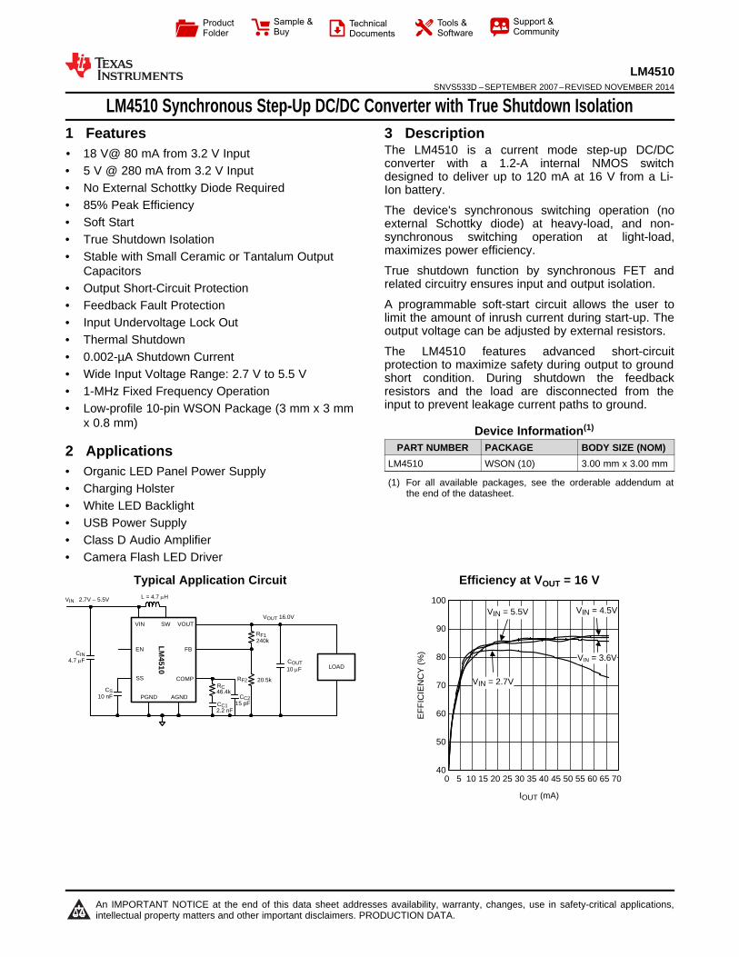
LM4510 Synchronous Step-Up DC/DC Converter with True Shutdown Isolation1 Features 3 Description
The LM4510 is a current mode step-up DC/DC1• 18 V@ 80 mA from 3.2 V Input
converter with a 1.2-A internal NMOS switch• 5 V @ 280 mA from 3.2 V Input designed to deliver up to 120 mA at 16 V from a Li-• No External Schottky Diode Required Ion battery.• 85% Peak Efficiency The device's synchronous switching operation (no• Soft Start external Schottky diode) at heavy-load, and non-
synchronous switching operation at light-load,• True Shutdown Isolationmaximizes power efficiency.• Stable with Small Ceramic or Tantalum OutputTrue shutdown function by synchronous FET andCapacitorsrelated circuitry ensures input and output isolation.• Output Short-Circuit ProtectionA programmable soft-start circuit allows the user to• Feedback Fault Protectionlimit the amount of inrush current during start-up. The• Input Undervoltage Lock Outoutput voltage can be adjusted by external resistors.
• Thermal ShutdownThe LM4510 features advanced short-circuit• 0.002-µA Shutdown Current protection to maximize safety during output to ground
• Wide Input Voltage Range: 2.7 V to 5.5 V short condition. During shutdown the feedback• 1-MHz Fixed Frequency Operation resistors and the load are disconnected from the
input to prevent leakage current paths to ground.• Low-profile 10-pin WSON Package (3 mm x 3 mmx 0.8 mm) Device Information(1)
PART NUMBER PACKAGE BODY SIZE (NOM)2 ApplicationsLM4510 WSON (10) 3.00 mm x 3.00 mm
• Organic LED Panel Power Supply(1) For all available packages, see the orderable addendum at• Charging Holster the end of the datasheet.
• White LED Backlight space• USB Power Supply
space• Class D Audio Amplifier• Camera Flash LED Driver
Typical Application Circuit Efficiency at VOUT = 16 V
1
An IMPORTANT NOTICE at the end of this data sheet addresses availability, warranty, changes, use in safety-critical applications,intellectual property matters and other important disclaimers. PRODUCTION DATA.

LM4510SNVS533D –SEPTEMBER 2007–REVISED NOVEMBER 2014 www.ti.com
Table of Contents7.3 Feature Description................................................. 101 Features .................................................................. 17.4 Device Functional Modes........................................ 112 Applications ........................................................... 1
8 Application and Implementation ........................ 133 Description ............................................................. 18.1 Application Information............................................ 134 Revision History..................................................... 28.2 Typical Applications ................................................ 135 Pin Configuration and Functions ......................... 3
9 Power Supply Recommendations ...................... 206 Specifications......................................................... 410 Layout................................................................... 206.1 Absolute Maximum Ratings ...................................... 4
10.1 Layout Guidelines ................................................. 206.2 Handling Ratings....................................................... 410.2 Layout Example .................................................... 206.3 Recommended Operating Conditions....................... 4
11 Device and Documentation Support ................. 216.4 Thermal Information .................................................. 511.1 Device Support...................................................... 216.5 Electrical Characteristics........................................... 511.2 Trademarks ........................................................... 216.6 Typical Characteristics .............................................. 711.3 Electrostatic Discharge Caution............................ 217 Detailed Description ............................................ 1011.4 Glossary ................................................................ 217.1 Overview ................................................................. 10
12 Mechanical, Packaging, and Orderable7.2 Functional Block Diagram ....................................... 10Information ........................................................... 21
4 Revision HistoryNOTE: Page numbers for previous revisions may differ from page numbers in the current version.
Changes from Revision C (May 2013) to Revision D Page
• Added Device Information and Handling Rating tables, Feature Description, Device Functional Modes, Applicationand Implementation, Power Supply Recommendations, Layout, Device and Documentation Support, andMechanical, Packaging, and Orderable Information sections; moved some curves to Application Curves section ............. 1
Changes from Revision B (May 2013) to Revision C Page
• Changed layout of National Data Sheet to TI format ........................................................................................................... 19
2 Submit Documentation Feedback Copyright © 2007–2014, Texas Instruments Incorporated
Product Folder Links: LM4510

1
2
3
4
5
10
9
8
7
6
Die-Attach Pad: GND
1
2
3
4
5
10
9
8
7
6
Die-Attach Pad: GND
SW
PGND
VIN
EN
SS
Top View Bottom View
VOUT
N/C
FB
COMP
AGND
LM4510www.ti.com SNVS533D –SEPTEMBER 2007–REVISED NOVEMBER 2014
5 Pin Configuration and Functions
WSON Package (DSC)10 Pins
Pin FunctionsPIN
DESCRIPTIONNO. NAME TYPE
1 SW A Switch pin. Drain connections of both internal NMOS and PMOS devices.2 PGND G Power ground3 VIN P Analog and Power supply input. Input range: 2.7 V to 5.5 V.4 EN I Enable logic input. HIGH= Enabled, LOW=Shutdown.5 SS A Soft-start pin6 AGND G Analog ground7 COMP A Compensation network connection.8 FB A Output voltage feedback connection.9 N/C No internal connection.10 VOUT A Internal PMOS source connection for synchronous rectification.
DAP DAP Die Attach Pad thermal connection
Copyright © 2007–2014, Texas Instruments Incorporated Submit Documentation Feedback 3
Product Folder Links: LM4510

LM4510SNVS533D –SEPTEMBER 2007–REVISED NOVEMBER 2014 www.ti.com
6 Specifications
6.1 Absolute Maximum Ratings (1) (2) (3)
MIN MAX UNITVIN −0.3 6.5 VVOUT −0.3 21 VSW (4) –0.3 VOUT+0.3 VEN, SS, COMP FB −0.3 6.5 VPGND to AGND −0.2 0.2 VContinuous power dissipation (5) Internally
LimitedJunction temperature (TJ-MAX) 150 150 °CLead temperature (soldering, 10 sec) (6) 260 °C
(1) Absolute maximum ratings are limits beyond which damage to the device may occur. Recommended Operating Conditions areconditions for which the device is intended to be functional. For specifications and test conditions, see the Electrical Characteristics.
(2) All voltages are with respect to the potential at the GND pin.(3) If Military/Aerospace specified devices are required, please contact the Texas Instruments Sales Office/ Distributors for availability and
specifications.(4) This condition applies if VIN < VOUT. If VIN > VOUT, a voltage greater than VIN + 0.3 V should not be applied to the VOUT or SW pins.
The absolute maximum specification applies to DC voltage. An extended negative voltage limit of –1 V applies for a pulse of up to 1 µs,and –2 V for a pulse of up to 40 ns. An extended positive voltage limit of 22 V applies for a pulse of up to 20 ns.
(5) Internal thermal shutdown circuitry protects the device from permanent damage. Thermal shutdown engages at TJ= 150°C (Typ.) anddisengages at TJ= 140°C (Typ.).
(6) For detailed soldering information and specifications, please refer to Application Note 1187: Leadless Leadframe Package (LLP)(SNOI401).
6.2 Handling RatingsMIN MAX UNIT
Tstg Storage temperature range –65 150 °CHuman body model (HBM), per ANSI/ESDA/JEDEC JS- 2 kV001, all pins (1)
V(ESD) Electrostatic discharge Charged device model (CDM), per JEDEC specification 1000 VJESD22-C101, all pins (2)
Machine model 200 V
(1) JEDEC document JEP155 states that 500-V HBM allows safe manufacturing with a standard ESD control process.(2) JEDEC document JEP157 states that 250-V CDM allows safe manufacturing with a standard ESD control process.
6.3 Recommended Operating ConditionsMIN MAX UNIT
Supply voltage (VIN) 2.7 5.5 VJunction temperature (TJ) (1) −40 125 °COutput voltage (VOUT) 18 V
(1) In applications where high power dissipation and/or poor package thermal resistance is present, the maximum ambient temperature mayhave to be derated. Maximum ambient temperature (TA-MAX) is dependent on the maximum operating junction temperature (TJ-MAX-OP =125°C), the maximum power dissipation of the device in the application (PD-MAX), and the junction-to ambient thermal resistance of thepart/package in the application (RθJA), as given by the following equation: TA-MAX = TJ-MAX-OP – (RθJA × PD-MAX)
4 Submit Documentation Feedback Copyright © 2007–2014, Texas Instruments Incorporated
Product Folder Links: LM4510

LM4510www.ti.com SNVS533D –SEPTEMBER 2007–REVISED NOVEMBER 2014
6.4 Thermal InformationLM4510
THERMAL METRIC (1) DSC UNIT10 PINS
RθJA Junction-to-ambient thermal resistance 36RθJC(top) Junction-to-case (top) thermal resistance 48.3RθJB Junction-to-board thermal resistance 22
°C/WψJT Junction-to-top characterization parameter 0.6ψJB Junction-to-board characterization parameter 22.1RθJC(bot) Junction-to-case (bottom) thermal resistance 3.8
(1) For more information about traditional and new thermal metrics, see the IC Package Thermal Metrics application report, SPRA953.
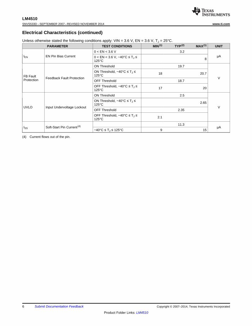
6.5 Electrical CharacteristicsUnless otherwise stated the following conditions apply: VIN = 3.6 V, EN = 3.6 V, TJ = 25°C.
PARAMETER TEST CONDITIONS MIN (1) TYP (2) MAX (1) UNIT2.7 V ≤ VIN ≤ 5.5 V 1.265
VFB FB Pin Voltage V2.7 V ≤ VIN ≤ 5.5 V, −40°C ≤ 1.24 1.29TJ ≤ 125°CIFB FB Pin Bias Current (3) −40°C ≤ TJ ≤ 125°C 0.050 1.5 µA
NMOS Switch RDS(on) ISW = 0.3 A 0.45 1.1RDS(on) Ω
PMOS Switch RDS(on) ISW = 0.3 A, VOUT = 10 V 0.9 1.1ICL NMOS Switch Current Limit 1 1.2 1.8 A
EN = 3.6 V, FB = COMP 1.7Device Switching EN = 3.6 V, FB = COMP, 2.5−40°C ≤ TJ ≤ 125°C
mAIQ EN = 3.6 V, FB > 1.29 V 0.8
Non-switching Current EN = 3.6 V, FB > 1.29 V, 2−40°C ≤ TJ ≤ 125°CShutdown Current EN = 0 V 0.002 0.050 µA
IL SW Leakage Current (3) SW = 20 V 0.01 0.150 µAVOUT = 20 V 90
IVOUT VOUT Bias Current (3) µAVOUT = 20 V, −40°C ≤ TJ ≤ 50 150125°CPMOS Switch Leakage SW = 0 V, VOUT = 20 VIVL 0.001 0.100 µACurrent
1fSW Switching Frequency MHz
−40°C ≤ TJ ≤ 125°C 0.85 1.2FB = 0 V 94%
DMAX Maximum Duty CycleFB = 0 V, −40°C ≤ TJ ≤ 125°C 88%
DMIN Minimum Duty Cycle 15% 20%130Error AmplifierGm µmhoTransconductance −40°C ≤ TJ ≤ 125°C 70 200
HIGH 0.81Device Enable
HIGH, −40°C ≤ TJ ≤ 125°C 1.2EN VThreshold LOW 0.78Device Shutdown
LOW, −40°C ≤ TJ ≤ 125°C 0.4
(1) All room temperature limits are production tested, specified through statistical analysis or by design. All limits at −40°C ≤ TJ ≤ 125°C arespecified via correlation using standard Statistical Quality Control (SQC) methods. All limits are used to calculate Average OutgoingQuality Level (AOQL).
(2) Typical numbers are at 25°C and represent the most likely norm.(3) Current flows into the pin.
Copyright © 2007–2014, Texas Instruments Incorporated Submit Documentation Feedback 5
Product Folder Links: LM4510
LM4510SNVS533D –SEPTEMBER 2007–REVISED NOVEMBER 2014 www.ti.com
Electrical Characteristics (continued)Unless otherwise stated the following conditions apply: VIN = 3.6 V, EN = 3.6 V, TJ = 25°C.
PARAMETER TEST CONDITIONS MIN (1) TYP (2) MAX (1) UNIT0 < EN < 3.6 V 3.2
IEN EN Pin Bias Current µA0 < EN < 3.6 V, −40°C ≤ TJ ≤ 8125°CON Threshold 19.7ON Threshold, −40°C ≤ TJ ≤ 18 20.7125°CFB Fault Feedback Fault Protection VProtection OFF Threshold 18.7OFF Threshold, −40°C ≤ TJ ≤ 17 20125°CON Threshold 2.5ON Threshold, −40°C ≤ TJ ≤ 2.65125°C
UVLO Input Undervoltage Lockout VOFF Threshold 2.35OFF Threshold, −40°C ≤ TJ ≤ 2.1125°C
11.3ISS Soft-Start Pin Current (4) µA
−40°C ≤ TJ ≤ 125°C 9 15
(4) Current flows out of the pin.
6 Submit Documentation Feedback Copyright © 2007–2014, Texas Instruments Incorporated
Product Folder Links: LM4510
TEMPERATURE (°C)
FR
EQ
UE
NC
Y (
MH
z)
1.03
1.02
1.01
1.00
0.99
0.98
0.97
0.96
0.95
0.94
0.93
0.92-40 -20 0 20 40 60 80 100
Frequency at VIN = 2.7V
Frequency at VIN = 3.6V
Frequency at VIN = 4.5V
IOUT (mA)
VO
UT (
V)
16.24
16.22
16.20
16.18
16.16
16.14
16.12
16.100 20 40 60 80
VIN = 5.5VVIN = 4.5V
VIN = 2.7V
VIN = 3.0V
VIN = 3.6V
90°C
-35°C
25°C
2 2.5 3.5 4.5 5.53 54 60
50
100
150
200
250
300
350
400
450
VIN (V)
I OU
T M
AX
(m
A)
TEMPERATURE (°C)
VO
UT
(V)
17.04
17.02
17.00
16.98
16.96
16.94
16.92
16.90
16.88
16.86
16.84-60 -40 -20 0 20 40 60 80 100
IOUT = 100 mA
IOUT = 10 mA
IOUT = 50 mA
TEMPERATURE (°C)
RD
S(O
N) (
mÖ)
1200
1000
800
600
400
200
0-40 -20 0 20 40 60 80 100
PMOS VIN = 3.6V
NMOS VIN = 3.6V
0.8
1.0
1.2
1.4
1.6
1.8
2.0
2.2
2.4
2.6
2.8
2.8 3.2 3.6 4 4.4 4.8 5.2
I Q (
mA
)
VIN (V)
IQ at 85°C
IQ at 25°C
IQ at -35°C
5.6
LM4510www.ti.com SNVS533D –SEPTEMBER 2007–REVISED NOVEMBER 2014
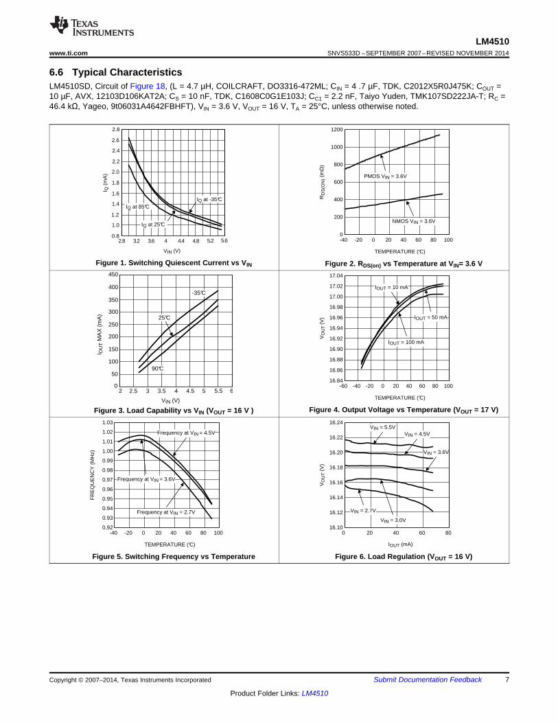
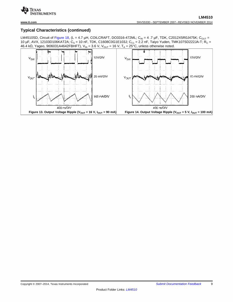
6.6 Typical CharacteristicsLM4510SD, Circuit of Figure 18, (L = 4.7 µH, COILCRAFT, DO3316-472ML; CIN = 4 .7 µF, TDK, C2012X5R0J475K; COUT =10 µF, AVX, 12103D106KAT2A; CS = 10 nF, TDK, C1608C0G1E103J; CC1 = 2.2 nF, Taiyo Yuden, TMK107SD222JA-T; RC =46.4 kΩ, Yageo, 9t06031A4642FBHFT), VIN = 3.6 V, VOUT = 16 V, TA = 25°C, unless otherwise noted.
Figure 1. Switching Quiescent Current vs VIN Figure 2. RDS(on) vs Temperature at VIN= 3.6 V
Figure 4. Output Voltage vs Temperature (VOUT = 17 V)Figure 3. Load Capability vs VIN (VOUT = 16 V )
Figure 5. Switching Frequency vs Temperature Figure 6. Load Regulation (VOUT = 16 V)
Copyright © 2007–2014, Texas Instruments Incorporated Submit Documentation Feedback 7
Product Folder Links: LM4510
VIN (V)
VO
UT
(V
)
5.040
5.035
5.030
5.025
5.020
5.015
5.0102.5 2.7 2.9 3.1 3.3 3.5 3.7 3.9 4.1 4.3
IOUT = 10 mA
IOUT = 120 mA
IOUT = 240 mA
4.5
IOUT (mA)
VO
UT
(V
)
5.030
5.028
5.026
5.024
5.022
5.020
5.018
5.016
5.0140 50 100 150 200 250 300
VIN = 4.2V
VIN = 3.6V
VIN = 3.0V
VIN (V)
VO
UT
(V)
16.25
16.23
16.21
16.19
16.17
16.152.5 3.0 3.5 4.0 4.5 5.0 5.5 6.0
IOUT = 30 mA
IOUT = 10 mA
IOUT = 70 mA
IOUT = 50 mA
LM4510SNVS533D –SEPTEMBER 2007–REVISED NOVEMBER 2014 www.ti.com
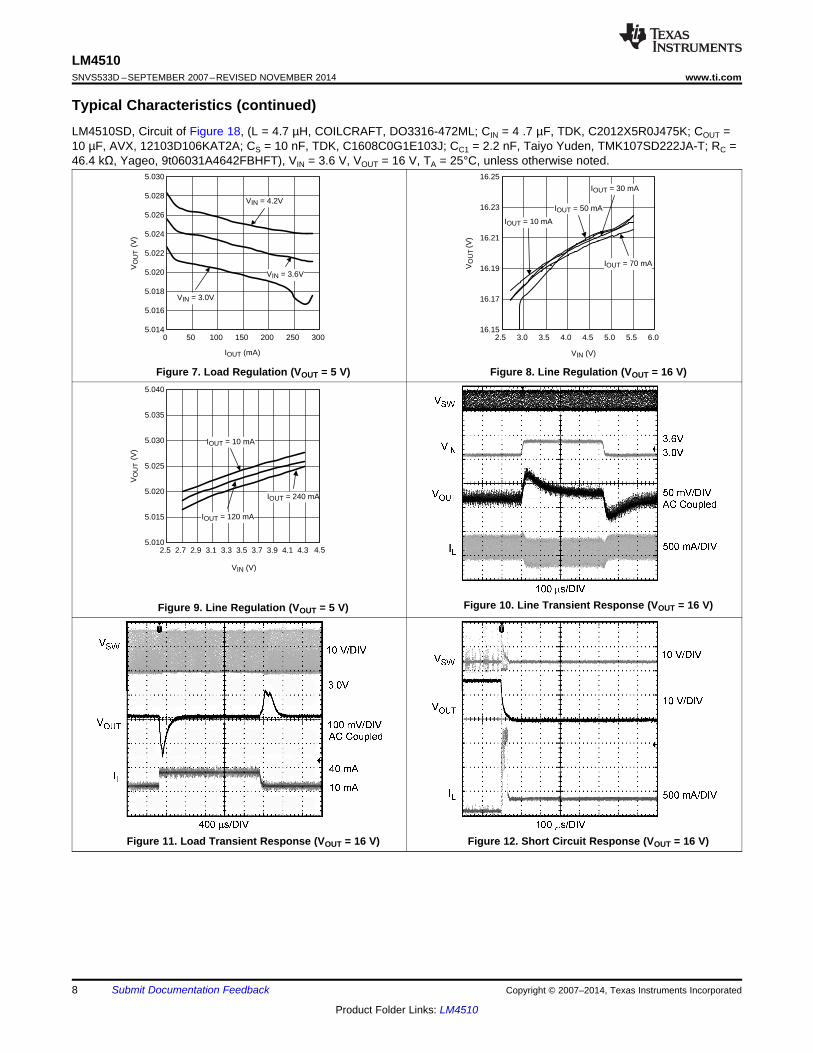
Typical Characteristics (continued)LM4510SD, Circuit of Figure 18, (L = 4.7 µH, COILCRAFT, DO3316-472ML; CIN = 4 .7 µF, TDK, C2012X5R0J475K; COUT =10 µF, AVX, 12103D106KAT2A; CS = 10 nF, TDK, C1608C0G1E103J; CC1 = 2.2 nF, Taiyo Yuden, TMK107SD222JA-T; RC =46.4 kΩ, Yageo, 9t06031A4642FBHFT), VIN = 3.6 V, VOUT = 16 V, TA = 25°C, unless otherwise noted.
Figure 7. Load Regulation (VOUT = 5 V) Figure 8. Line Regulation (VOUT = 16 V)
Figure 10. Line Transient Response (VOUT = 16 V)Figure 9. Line Regulation (VOUT = 5 V)
Figure 11. Load Transient Response (VOUT = 16 V) Figure 12. Short Circuit Response (VOUT = 16 V)
8 Submit Documentation Feedback Copyright © 2007–2014, Texas Instruments Incorporated
Product Folder Links: LM4510
LM4510www.ti.com SNVS533D –SEPTEMBER 2007–REVISED NOVEMBER 2014
Typical Characteristics (continued)LM4510SD, Circuit of Figure 18, (L = 4.7 µH, COILCRAFT, DO3316-472ML; CIN = 4 .7 µF, TDK, C2012X5R0J475K; COUT =10 µF, AVX, 12103D106KAT2A; CS = 10 nF, TDK, C1608C0G1E103J; CC1 = 2.2 nF, Taiyo Yuden, TMK107SD222JA-T; RC =46.4 kΩ, Yageo, 9t06031A4642FBHFT), VIN = 3.6 V, VOUT = 16 V, TA = 25°C, unless otherwise noted.
Figure 13. Output Voltage Ripple (VOUT = 16 V, IOUT = 90 mA) Figure 14. Output Voltage Ripple (VOUT = 5 V, IOUT = 100 mA)
Copyright © 2007–2014, Texas Instruments Incorporated Submit Documentation Feedback 9
Product Folder Links: LM4510

LOGIC
SYNC/NON-SYNC
BO
DY
DIO
DE
CT
RL
and
TR
UE
S/D
PWM
Ramp
AGND
CURRENTLIMIT
10 uA
SW
COMP
VIN
PGND
EN
FB
S/D
OSC
UVP
SCP
Current Sense
UVP REF
BGBG
TSD
+-
+-
+-
+-
Feedback Fault Protection
RESET SET
EAMP
REF
SS VOUT
Q
QR
S
LM4510SNVS533D –SEPTEMBER 2007–REVISED NOVEMBER 2014 www.ti.com
7 Detailed Description
7.1 OverviewLM4510 is a peak current-mode, fixed-frequency PWM boost regulator that employs both Synchronous and Non-Synchronous Switching.
The DC/DC regulator regulates the feedback output voltage providing excellent line and load transient response.The operation of the LM4510 can best be understood by referring to the Block Diagram.
7.2 Functional Block Diagram
7.3 Feature Description
7.3.1 Short Circuit ProtectionWhen VOUT goes down to VIN–0.7V (typ.), the device stops switching due to the short-circuit protection circuitryand the short-circuit output current is limited to IINIT_CHARGE.
10 Submit Documentation Feedback Copyright © 2007–2014, Texas Instruments Incorporated
Product Folder Links: LM4510

ON
OFF
+- +-
PWM
NMOSPMOS
VOUT
GND
VSW1
+- COUT
RLOAD
LM4510www.ti.com SNVS533D –SEPTEMBER 2007–REVISED NOVEMBER 2014
Feature Description (continued)7.3.2 Feedback Fault ProtectionThe LM4510 features unique Feedback Fault Protection to maximize safety when the feedback resistor is notproperly connected to a circuit or the feedback node is shorted directly to ground.
Feedback fault triggers VOUT monitoring. During monitoring, if VOUT reaches a protection level, the device shutsdown. When the feedback network is reconnected and VOUT is lower than the OFF threshold level of FeedbackFault Protection, VOUT monitoring stops. VOUT is then regulated by the control loop.
7.3.3 Input Undervoltage Lock-OutThe LM4510 has dedicated circuitry to protect the IC and the external components when the battery voltage islower than the preset threshold. This undervoltage lock-out with hysteresis prevents malfunctions during start-upor abnormal power off.
7.3.4 Thermal ShutdownIf the die temperature exceeds 150°C (typ.), the thermal protection circuitry shuts down the device. The switchesremain off until the die temperature is reduced to approximately 140°C (typ.).
7.4 Device Functional Modes
7.4.1 Non-Synchronous OperationThe device operates in Non-synchronous Mode at light load (IOUT < 10 mA) or when output voltage is lower than10 V (typ.). At light load, LM4510 automatically changes its switching operation from 'Synchronous' to 'Non-Synchronous' depending on VIN and L. Non-Synchronous operation at light load maximizes power efficiency byreducing PMOS driving loss.
7.4.2 Operation in Synchronous Continuous Conduction Mode (Cycle 1, Cycle 2)
Figure 15. Schematic of Synchronous Boost Converter
Synchronous boost converter is shown in Figure 15. At the start of each cycle, the oscillator sets the driver logicand turns on the NMOS power device and turns off the PMOS power device.
7.4.2.1 Cycle 1 DescriptionRefer to Figure 16. NMOS switch turn-on → Inductor current increases and flows to GND.
PMOS switch turn-off → Isolate VOUT from SW → Output capacitor supplies load current.
Figure 16. Equivalent Circuit During Cycle 1Copyright © 2007–2014, Texas Instruments Incorporated Submit Documentation Feedback 11
Product Folder Links: LM4510
OFF
ON
LM4510SNVS533D –SEPTEMBER 2007–REVISED NOVEMBER 2014 www.ti.com
Device Functional Modes (continued)During operation, EAMP output voltage (VCOMP) increases for larger loads and decreases for smaller loads.When the sum of the ramp compensation and the sensed NMOS current reaches a level determined by theEAMP output voltage, the PWM COMP resets the logic, turning off the NMOS power device and turning on thePMOS power device.
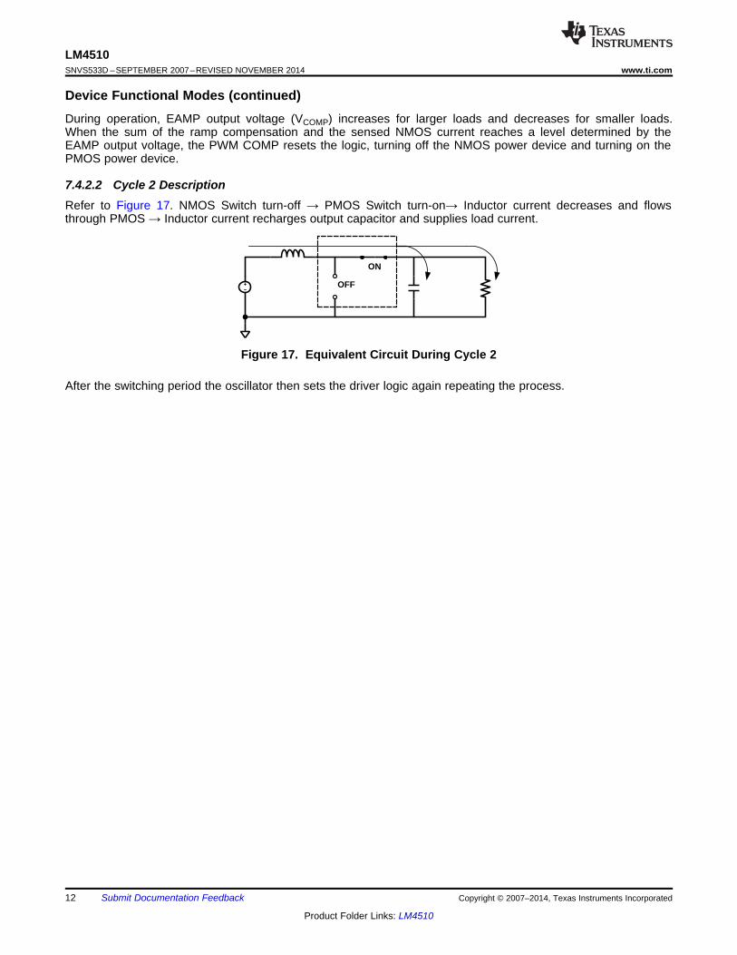
7.4.2.2 Cycle 2 DescriptionRefer to Figure 17. NMOS Switch turn-off → PMOS Switch turn-on→ Inductor current decreases and flowsthrough PMOS → Inductor current recharges output capacitor and supplies load current.
Figure 17. Equivalent Circuit During Cycle 2
After the switching period the oscillator then sets the driver logic again repeating the process.
12 Submit Documentation Feedback Copyright © 2007–2014, Texas Instruments Incorporated
Product Folder Links: LM4510
VIN 2.7V ± 5.5V
4.7 PF
LM
4500
LOAD
PGND
EN
AGND
COMPSS
FB
L = 4.7 PH
VIN SW VOUT
CIN
CS
LM
4510
RF1
RF2
CC1
RC
CC2
VOUT 16.0V
COUT10 PF
240k
20.5k
46.4k
2.2 nF15 pF
10 nF
LM4510www.ti.com SNVS533D –SEPTEMBER 2007–REVISED NOVEMBER 2014
8 Application and Implementation
NOTEInformation in the following applications sections is not part of the TI componentspecification, and TI does not warrant its accuracy or completeness. TI’s customers areresponsible for determining suitability of components for their purposes. Customers shouldvalidate and test their design implementation to confirm system functionality.
8.1 Application InformationThe LM4510 shuts down when the EN pin is low. In this mode the feedback resistors and the load aredisconnected from the input in order to avoid leakage current flow and to allow the output voltage to drop to 0 V.
The LM4510 turns on when EN is high. There is an internal pull-down resistor on the EN pin so the device is in anormally off state.
8.2 Typical Applications
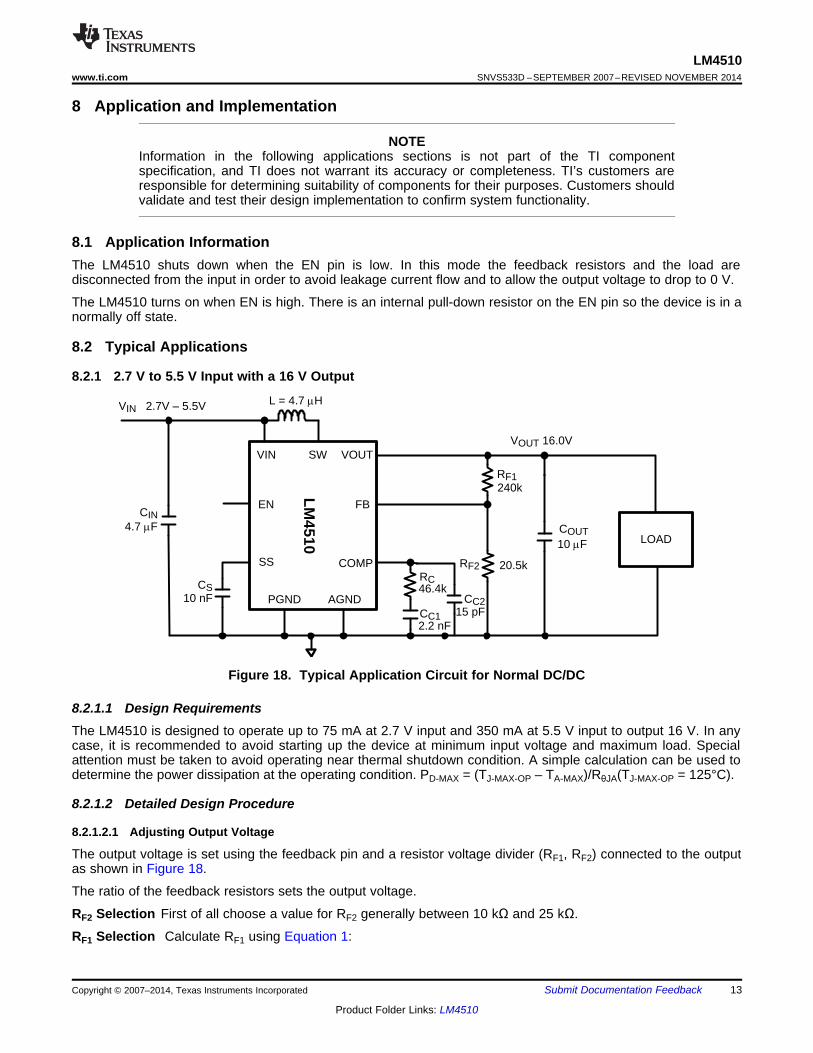
8.2.1 2.7 V to 5.5 V Input with a 16 V Output
Figure 18. Typical Application Circuit for Normal DC/DC
8.2.1.1 Design RequirementsThe LM4510 is designed to operate up to 75 mA at 2.7 V input and 350 mA at 5.5 V input to output 16 V. In anycase, it is recommended to avoid starting up the device at minimum input voltage and maximum load. Specialattention must be taken to avoid operating near thermal shutdown condition. A simple calculation can be used todetermine the power dissipation at the operating condition. PD-MAX = (TJ-MAX-OP – TA-MAX)/RθJA(TJ-MAX-OP = 125°C).
8.2.1.2 Detailed Design Procedure
8.2.1.2.1 Adjusting Output Voltage
The output voltage is set using the feedback pin and a resistor voltage divider (RF1, RF2) connected to the outputas shown in Figure 18.
The ratio of the feedback resistors sets the output voltage.
RF2 Selection First of all choose a value for RF2 generally between 10 kΩ and 25 kΩ.
RF1 Selection Calculate RF1 using Equation 1:
Copyright © 2007–2014, Texas Instruments Incorporated Submit Documentation Feedback 13
Product Folder Links: LM4510
OUT
INOUT
V
VV=D
-x],A[
fL
DV=I
SW
INL'
x
],x OUT
IN
V
V='DA[
D¿
I=I
OUTAVE_L
K
IOUT_Max = VOUT
1.32 x VIN - 2.79[A]
][Rx)- 1V
V(=R 2F
FB
OF1 :
LM4510SNVS533D –SEPTEMBER 2007–REVISED NOVEMBER 2014 www.ti.com
Typical Applications (continued)
(1)
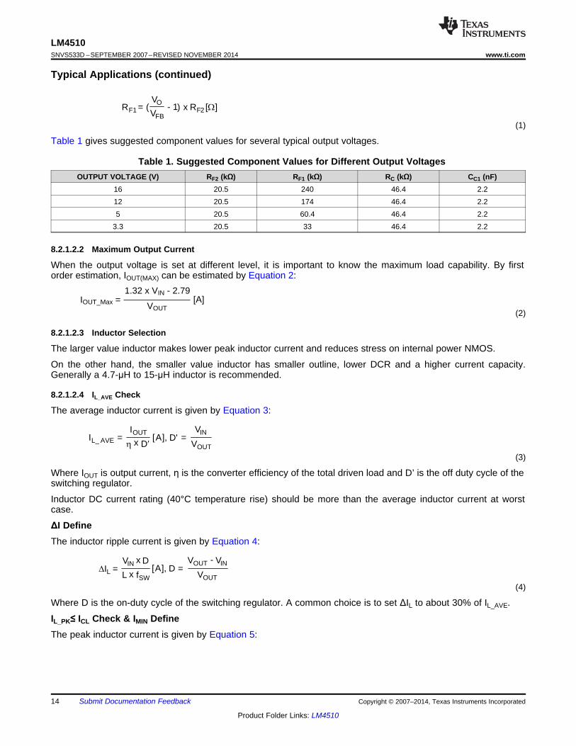
Table 1 gives suggested component values for several typical output voltages.
Table 1. Suggested Component Values for Different Output VoltagesOUTPUT VOLTAGE (V) RF2 (kΩ) RF1 (kΩ) RC (kΩ) CC1 (nF)
16 20.5 240 46.4 2.212 20.5 174 46.4 2.25 20.5 60.4 46.4 2.2
3.3 20.5 33 46.4 2.2
8.2.1.2.2 Maximum Output Current
When the output voltage is set at different level, it is important to know the maximum load capability. By firstorder estimation, IOUT(MAX) can be estimated by Equation 2:
(2)
8.2.1.2.3 Inductor Selection
The larger value inductor makes lower peak inductor current and reduces stress on internal power NMOS.
On the other hand, the smaller value inductor has smaller outline, lower DCR and a higher current capacity.Generally a 4.7-μH to 15-μH inductor is recommended.
8.2.1.2.4 IL_AVE Check
The average inductor current is given by Equation 3:
(3)
Where IOUT is output current, η is the converter efficiency of the total driven load and D’ is the off duty cycle of theswitching regulator.
Inductor DC current rating (40°C temperature rise) should be more than the average inductor current at worstcase.
ΔI DefineThe inductor ripple current is given by Equation 4:
(4)
Where D is the on-duty cycle of the switching regulator. A common choice is to set ΔIL to about 30% of IL_AVE.
IL_PK≤ ICL Check & IMIN DefineThe peak inductor current is given by Equation 5:
14 Submit Documentation Feedback Copyright © 2007–2014, Texas Instruments Incorporated
Product Folder Links: LM4510
12
D+_I RMSCOUT = )1( D- »
¼
º»¼
º 2IOUT 2)1( D-
2IL'][ A
]A[12
=I RMS_CINIL'
]A[fL2
DV+
D¿
I=I
SW
INOUTpk_L K
x
xx
]A[2I
+I=I LAVE_Lpk_L
'
LM4510www.ti.com SNVS533D –SEPTEMBER 2007–REVISED NOVEMBER 2014
(5)
To prevent loss of regulation, ensure that the NMOS power switch current limit is greater than the worst-casepeak inductor current in the target application.
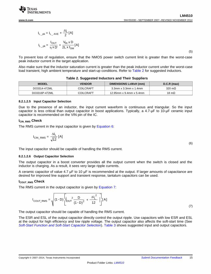
Also make sure that the inductor saturation current is greater than the peak inductor current under the worst-caseload transient, high ambient temperature and start-up conditions. Refer to Table 2 for suggested inductors.
Table 2. Suggested Inductors and Their SuppliersMODEL VENDOR DIMENSIONS LxWxH (mm) D.C.R (max)
DO3314-472ML COILCRAFT 3.3mm x 3.3mm x 1.4mm 320 mΩDO3316P-472ML COILCRAFT 12.95mm x 9.4mm x 5.4mm 18 mΩ
8.2.1.2.5 Input Capacitor Selection
Due to the presence of an inductor, the input current waveform is continuous and triangular. So the inputcapacitor is less critical than output capacitor in boost applications. Typically, a 4.7-μF to 10-μF ceramic inputcapacitor is recommended on the VIN pin of the IC.
ICIN_RMS CheckThe RMS current in the input capacitor is given by Equation 6:
(6)
The input capacitor should be capable of handling the RMS current.
8.2.1.2.6 Output Capacitor Selection
The output capacitor in a boost converter provides all the output current when the switch is closed and theinductor is charging. As a result, it sees very large ripple currents.
A ceramic capacitor of value 4.7 μF to 10 μF is recommended at the output. If larger amounts of capacitance aredesired for improved line support and transient response, tantalum capacitors can be used.
ICOUT_RMS CheckThe RMS current in the output capacitor is given by Equation 7:
(7)
The output capacitor should be capable of handling the RMS current.
The ESR and ESL of the output capacitor directly control the output ripple. Use capacitors with low ESR and ESLat the output for high efficiency and low ripple voltage. The output capacitor also affects the soft-start time (SeeSoft-Start Function and Soft-Start Capacitor Selection). Table 3 shows suggested input and output capacitors.
Copyright © 2007–2014, Texas Instruments Incorporated Submit Documentation Feedback 15
Product Folder Links: LM4510
[sec]+)7.- 0V(xC
=tINOUT
SS I CHARGE_INIT I CHARGE_SS
VxC FBS
VEN
appropriate VOUT
Lin
ear
Cha
rgin
g P
erio
d
VSS = VFB
VOUT = VIN - 0.7V
VSS
Shu
tdow
n
Sof
t-S
tart
S
witc
hing
Per
iod
Nor
mal
Sw
itchi
ng
Ope
ratio
n
VSS = VIN
VOUT
LM4510SNVS533D –SEPTEMBER 2007–REVISED NOVEMBER 2014 www.ti.com
Table 3. Suggested CIN and COUT Capacitors and Their SuppliersVOLTAGE CASE SIZEMODEL TYPE VENDOR RATING INCH (mm)
4.7 µF for CIN
C2012X5R0J475 Ceramic, X5R TDK 6.3 V 0805 (2012)GRM21BR60J475 Ceramic, X5R muRata 6.3 V 0805 (2012)
JMK212BJ475 Ceramic, X5R Taiyo-Yuden 6.3 V 0805 (2012)C2012X5R0J475K Ceramic, X5R TDK 6.3 V 0603 (1608)
10 µF for COUT
TMK316BJ106KL Ceramic, X5R Taiyo-Yuden 25 V 1206 (3216)12103D106KAT2A Ceramic, X5R AVX 25 V 1210 (3225)
8.2.1.2.7 Soft-Start Function and Soft-Start Capacitor Selection
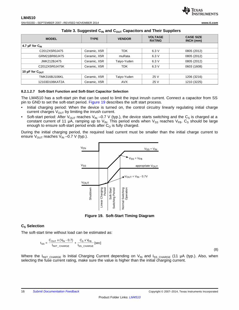
The LM4510 has a soft-start pin that can be used to limit the input inrush current. Connect a capacitor from SSpin to GND to set the soft-start period. Figure 19 describes the soft start process.• Initial charging period: When the device is turned on, the control circuitry linearly regulating initial charge
current charges VOUT by limiting the inrush current.• Soft-start period: After VOUT reaches VIN –0.7 V (typ.), the device starts switching and the CS is charged at a
constant current of 11 μA, ramping up to VIN. This period ends when VSS reaches VFB. CS should be largeenough to ensure soft-start period ends after CO is fully charged.
During the initial charging period, the required load current must be smaller than the initial charge current toensure VOUT reaches VIN –0.7 V (typ.).
Figure 19. Soft-Start Timing Diagram
CS SelectionThe soft-start time without load can be estimated as:
(8)
Where the IINIT_CHARGE is Initial Charging Current depending on VIN and ISS_CHARGE (11 μA (typ.). Also, whenselecting the fuse current rating, make sure the value is higher than the initial charging current.
16 Submit Documentation Feedback Copyright © 2007–2014, Texas Instruments Incorporated
Product Folder Links: LM4510

1=f 2PC ]Hz[
C)R//R(2 2COCS
1=fPC ]Hz[
C)R+R(2 1COCS
1=fZC ]Hz[
CR2 1CCS
LM4510www.ti.com SNVS533D –SEPTEMBER 2007–REVISED NOVEMBER 2014
8.2.1.2.8 Compensation Component Selection
The LM4510 provides a compensation pin COMP to customize the voltage loop feedback. It is recommendedthat a series combination of RC and CC1 be used for the compensation network, as shown in the typicalapplication circuit. In addition, CC2 is used for compensating high frequency zeros.
The series combination of RC and CC1 introduces a pole-zero pair according to Equation 9:
(9)
In addition, CC2 introduces a pole according to Equation 10:
(10)
Where RO is the output impedance of the error amplifier, approximately 1 MΩ, and amplifier voltage gain istypically 200 V/V depending on temperature and VIN.
Refer to Table 4 for suggested soft start capacitor and compensation components.
Table 4. Suggested CS and Compensation ComponentsCASE SIZEMODEL TYPE VENDOR VOLTAGE RATING INCH (mm)
(CS) C1608C0G1E103J Ceramic, X5R TDK 6.3 V 603 (1608)(C1)TMK107SD222JA-T Ceramic, X5R Taiyo Yuden 25 V 603 (1608)
(RC) 9t06031A4642FBHFT Resistor Yageo Corporation 1/10 W 603 (1608)
Copyright © 2007–2014, Texas Instruments Incorporated Submit Documentation Feedback 17
Product Folder Links: LM4510
IOUT = (mA)
EF
FIC
IEN
CY
(%
)
85
80
75
70
65
60
55
500 40 80 120 160 200 240 280
VIN = 4.2V
VIN = 3.6V
VIN = 3.0V
IOUT (mA)
EF
FIC
IEN
CY
(%
)100
90
80
70
60
50
400 5 10 15 20 25 30 35 40 45 50 55 60 65 70
VIN = 5.5V VIN = 4.5V
VIN = 2.7V
VIN = 3.6V
IOUT (mA)
EF
FIC
IEN
CY
(%
)
100
90
80
70
60
50
400 10 20 30 40 50 60 70 80 90 100
VIN = 4.5VVIN = 3.6V
VIN = 3.0V
VIN = 5.5V
LM4510SNVS533D –SEPTEMBER 2007–REVISED NOVEMBER 2014 www.ti.com
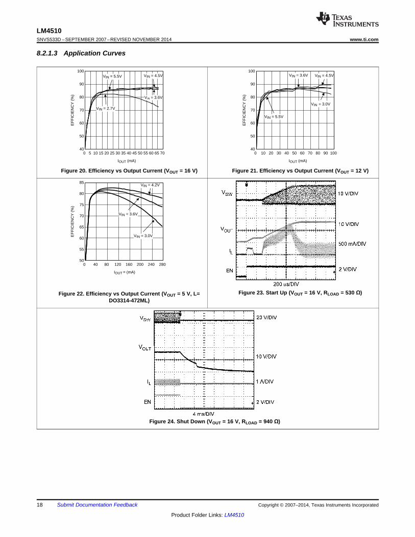
8.2.1.3 Application Curves
Figure 20. Efficiency vs Output Current (VOUT = 16 V) Figure 21. Efficiency vs Output Current (VOUT = 12 V)
Figure 23. Start Up (VOUT = 16 V, RLOAD = 530 Ω)Figure 22. Efficiency vs Output Current (VOUT = 5 V, L=DO3314-472ML)
Figure 24. Shut Down (VOUT = 16 V, RLOAD = 940 Ω)
18 Submit Documentation Feedback Copyright © 2007–2014, Texas Instruments Incorporated
Product Folder Links: LM4510

PGND AGND
COMPSS
FB
CIN
CS
L = 4.7 éH
RC
CC
RT RF
Battery or Power Source
Pull high for TORCHPull high for FLASH
VIN SW VOUT
EN
COUT
LM4510
50Ö 12.4Ö
10 éF4.7 éF
10 nF
46.6k
2.2 nF
Everlight47-23UWD/TR8
=ITorch ]A[VFB
RT
]A[=IFlash
VFB
R//R FT
LM4510www.ti.com SNVS533D –SEPTEMBER 2007–REVISED NOVEMBER 2014
8.2.2 Flash and Torch ApplicationLM4510 can be configured to drive white LEDs for the flash and torch functions. The flash/torch can be set upwith the circuit shown in Figure 25 by using the resistor RT to determine the current in Torch Mode and RF todetermine the current in Flash Mode. The amount of current can be estimated using Equation 11:
(11)
Figure 25. Typical Application Circuit for Flash/Torch
8.2.2.1 Design RequirementsSee Design Requirements.
8.2.2.2 Detailed Design ProcedureSee Detailed Design Procedure.
8.2.2.3 Application CurveSee Application Curves.
Copyright © 2007–2014, Texas Instruments Incorporated Submit Documentation Feedback 19
Product Folder Links: LM4510
LM4510SNVS533D –SEPTEMBER 2007–REVISED NOVEMBER 2014 www.ti.com
9 Power Supply RecommendationsThe power supply for the applications using the LM4510 device should be big enough considering output powerand efficiency at given input voltage condition. Minimum current requirement condition is (VOUT * IOUT)/(VIN *efficiency) and approximately 20 - 30% higher than this value is recommended
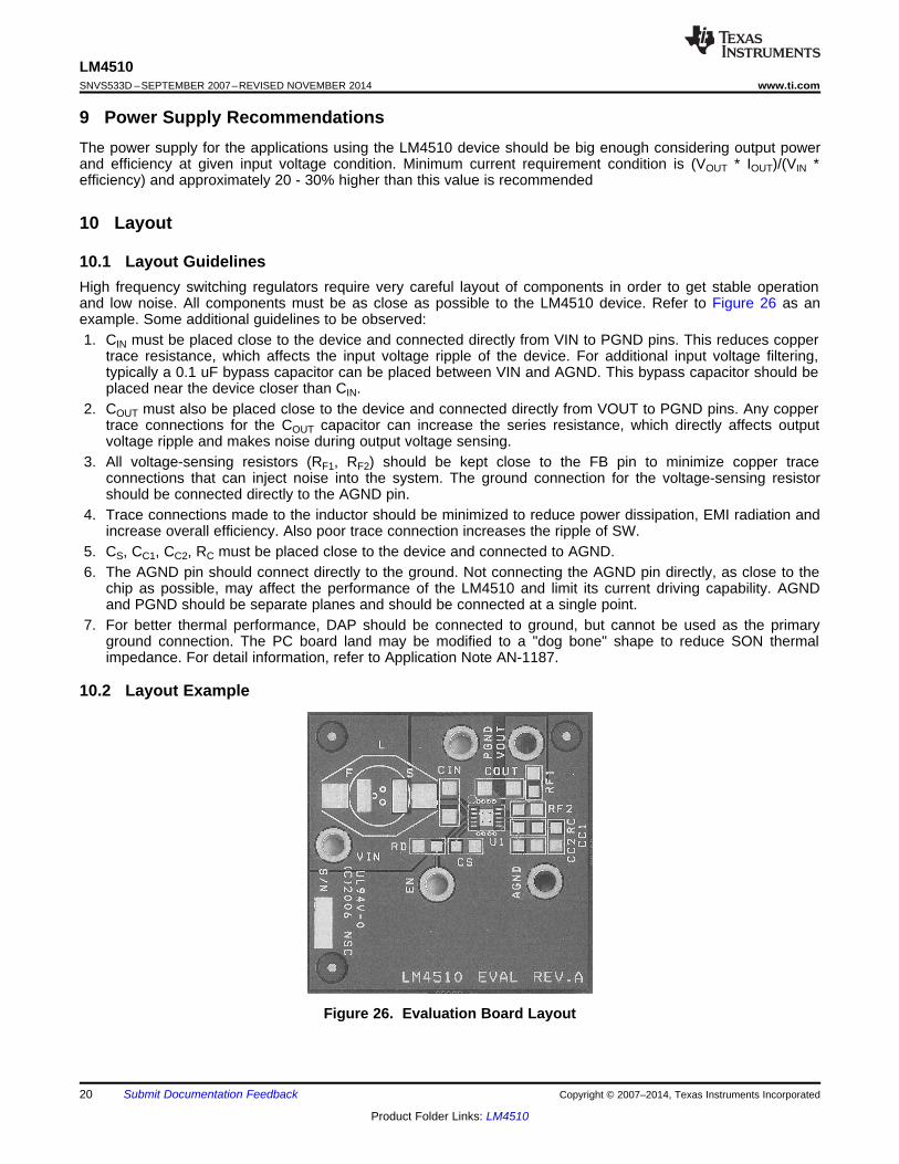
10 Layout
10.1 Layout GuidelinesHigh frequency switching regulators require very careful layout of components in order to get stable operationand low noise. All components must be as close as possible to the LM4510 device. Refer to Figure 26 as anexample. Some additional guidelines to be observed:1. CIN must be placed close to the device and connected directly from VIN to PGND pins. This reduces copper
trace resistance, which affects the input voltage ripple of the device. For additional input voltage filtering,typically a 0.1 uF bypass capacitor can be placed between VIN and AGND. This bypass capacitor should beplaced near the device closer than CIN.
2. COUT must also be placed close to the device and connected directly from VOUT to PGND pins. Any coppertrace connections for the COUT capacitor can increase the series resistance, which directly affects outputvoltage ripple and makes noise during output voltage sensing.
3. All voltage-sensing resistors (RF1, RF2) should be kept close to the FB pin to minimize copper traceconnections that can inject noise into the system. The ground connection for the voltage-sensing resistorshould be connected directly to the AGND pin.
4. Trace connections made to the inductor should be minimized to reduce power dissipation, EMI radiation andincrease overall efficiency. Also poor trace connection increases the ripple of SW.
5. CS, CC1, CC2, RC must be placed close to the device and connected to AGND.6. The AGND pin should connect directly to the ground. Not connecting the AGND pin directly, as close to the
chip as possible, may affect the performance of the LM4510 and limit its current driving capability. AGNDand PGND should be separate planes and should be connected at a single point.
7. For better thermal performance, DAP should be connected to ground, but cannot be used as the primaryground connection. The PC board land may be modified to a "dog bone" shape to reduce SON thermalimpedance. For detail information, refer to Application Note AN-1187.
10.2 Layout Example
Figure 26. Evaluation Board Layout
20 Submit Documentation Feedback Copyright © 2007–2014, Texas Instruments Incorporated
Product Folder Links: LM4510
LM4510www.ti.com SNVS533D –SEPTEMBER 2007–REVISED NOVEMBER 2014
11 Device and Documentation Support
11.1 Device Support
11.1.1 Third-Party Products DisclaimerTI'S PUBLICATION OF INFORMATION REGARDING THIRD-PARTY PRODUCTS OR SERVICES DOES NOTCONSTITUTE AN ENDORSEMENT REGARDING THE SUITABILITY OF SUCH PRODUCTS OR SERVICESOR A WARRANTY, REPRESENTATION OR ENDORSEMENT OF SUCH PRODUCTS OR SERVICES, EITHERALONE OR IN COMBINATION WITH ANY TI PRODUCT OR SERVICE.
11.2 TrademarksAll trademarks are the property of their respective owners.
11.3 Electrostatic Discharge CautionThese devices have limited built-in ESD protection. The leads should be shorted together or the device placed in conductive foamduring storage or handling to prevent electrostatic damage to the MOS gates.
11.4 GlossarySLYZ022 — TI Glossary.
This glossary lists and explains terms, acronyms, and definitions.
12 Mechanical, Packaging, and Orderable InformationThe following pages include mechanical, packaging, and orderable information. This information is the mostcurrent data available for the designated devices. This data is subject to change without notice and revision ofthis document. For browser-based versions of this data sheet, refer to the left-hand navigation.
Copyright © 2007–2014, Texas Instruments Incorporated Submit Documentation Feedback 21
Product Folder Links: LM4510
PACKAGE OPTION ADDENDUM
www.ti.com 10-Dec-2020
Addendum-Page 1
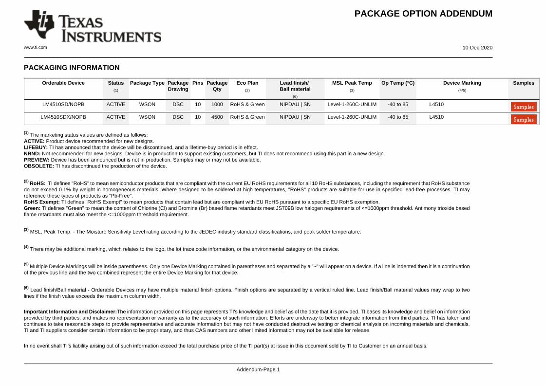
PACKAGING INFORMATION
Orderable Device Status(1)
Package Type PackageDrawing
Pins PackageQty
Eco Plan(2)
Lead finish/Ball material
(6)
MSL Peak Temp(3)
Op Temp (°C) Device Marking(4/5)
Samples
LM4510SD/NOPB ACTIVE WSON DSC 10 1000 RoHS & Green NIPDAU | SN Level-1-260C-UNLIM -40 to 85 L4510
LM4510SDX/NOPB ACTIVE WSON DSC 10 4500 RoHS & Green NIPDAU | SN Level-1-260C-UNLIM -40 to 85 L4510
(1) The marketing status values are defined as follows:ACTIVE: Product device recommended for new designs.LIFEBUY: TI has announced that the device will be discontinued, and a lifetime-buy period is in effect.NRND: Not recommended for new designs. Device is in production to support existing customers, but TI does not recommend using this part in a new design.PREVIEW: Device has been announced but is not in production. Samples may or may not be available.OBSOLETE: TI has discontinued the production of the device.
(2) RoHS: TI defines "RoHS" to mean semiconductor products that are compliant with the current EU RoHS requirements for all 10 RoHS substances, including the requirement that RoHS substancedo not exceed 0.1% by weight in homogeneous materials. Where designed to be soldered at high temperatures, "RoHS" products are suitable for use in specified lead-free processes. TI mayreference these types of products as "Pb-Free".RoHS Exempt: TI defines "RoHS Exempt" to mean products that contain lead but are compliant with EU RoHS pursuant to a specific EU RoHS exemption.Green: TI defines "Green" to mean the content of Chlorine (Cl) and Bromine (Br) based flame retardants meet JS709B low halogen requirements of <=1000ppm threshold. Antimony trioxide basedflame retardants must also meet the <=1000ppm threshold requirement.
(3) MSL, Peak Temp. - The Moisture Sensitivity Level rating according to the JEDEC industry standard classifications, and peak solder temperature.
(4) There may be additional marking, which relates to the logo, the lot trace code information, or the environmental category on the device.
(5) Multiple Device Markings will be inside parentheses. Only one Device Marking contained in parentheses and separated by a "~" will appear on a device. If a line is indented then it is a continuationof the previous line and the two combined represent the entire Device Marking for that device.
(6) Lead finish/Ball material - Orderable Devices may have multiple material finish options. Finish options are separated by a vertical ruled line. Lead finish/Ball material values may wrap to twolines if the finish value exceeds the maximum column width.
Important Information and Disclaimer:The information provided on this page represents TI's knowledge and belief as of the date that it is provided. TI bases its knowledge and belief on informationprovided by third parties, and makes no representation or warranty as to the accuracy of such information. Efforts are underway to better integrate information from third parties. TI has taken andcontinues to take reasonable steps to provide representative and accurate information but may not have conducted destructive testing or chemical analysis on incoming materials and chemicals.TI and TI suppliers consider certain information to be proprietary, and thus CAS numbers and other limited information may not be available for release.
In no event shall TI's liability arising out of such information exceed the total purchase price of the TI part(s) at issue in this document sold by TI to Customer on an annual basis.
PACKAGE OPTION ADDENDUM
www.ti.com 10-Dec-2020
Addendum-Page 2
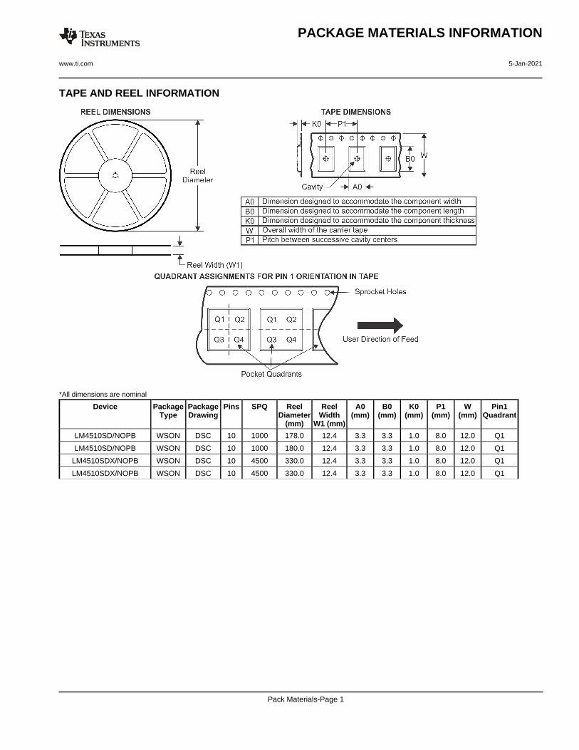
TAPE AND REEL INFORMATION
*All dimensions are nominal
Device PackageType
PackageDrawing
Pins SPQ ReelDiameter
(mm)
ReelWidth
W1 (mm)
A0(mm)
B0(mm)
K0(mm)
P1(mm)
W(mm)
Pin1Quadrant
LM4510SD/NOPB WSON DSC 10 1000 178.0 12.4 3.3 3.3 1.0 8.0 12.0 Q1
LM4510SD/NOPB WSON DSC 10 1000 180.0 12.4 3.3 3.3 1.0 8.0 12.0 Q1
LM4510SDX/NOPB WSON DSC 10 4500 330.0 12.4 3.3 3.3 1.0 8.0 12.0 Q1
LM4510SDX/NOPB WSON DSC 10 4500 330.0 12.4 3.3 3.3 1.0 8.0 12.0 Q1
PACKAGE MATERIALS INFORMATION
www.ti.com 5-Jan-2021
Pack Materials-Page 1
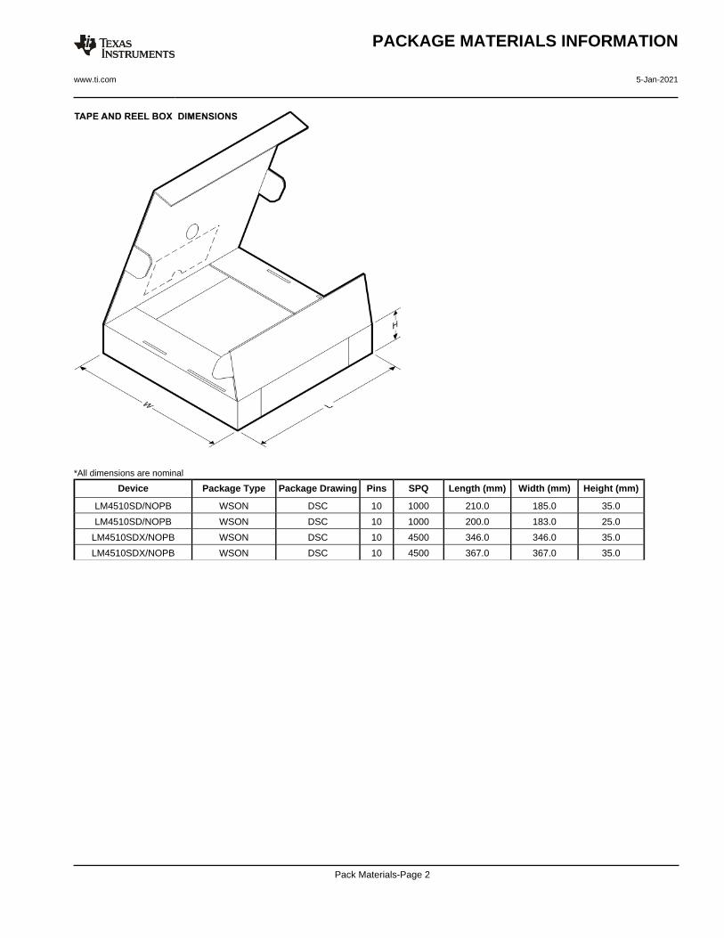
*All dimensions are nominal
Device Package Type Package Drawing Pins SPQ Length (mm) Width (mm) Height (mm)
LM4510SD/NOPB WSON DSC 10 1000 210.0 185.0 35.0
LM4510SD/NOPB WSON DSC 10 1000 200.0 183.0 25.0
LM4510SDX/NOPB WSON DSC 10 4500 346.0 346.0 35.0
LM4510SDX/NOPB WSON DSC 10 4500 367.0 367.0 35.0
PACKAGE MATERIALS INFORMATION
www.ti.com 5-Jan-2021
Pack Materials-Page 2
www.ti.com
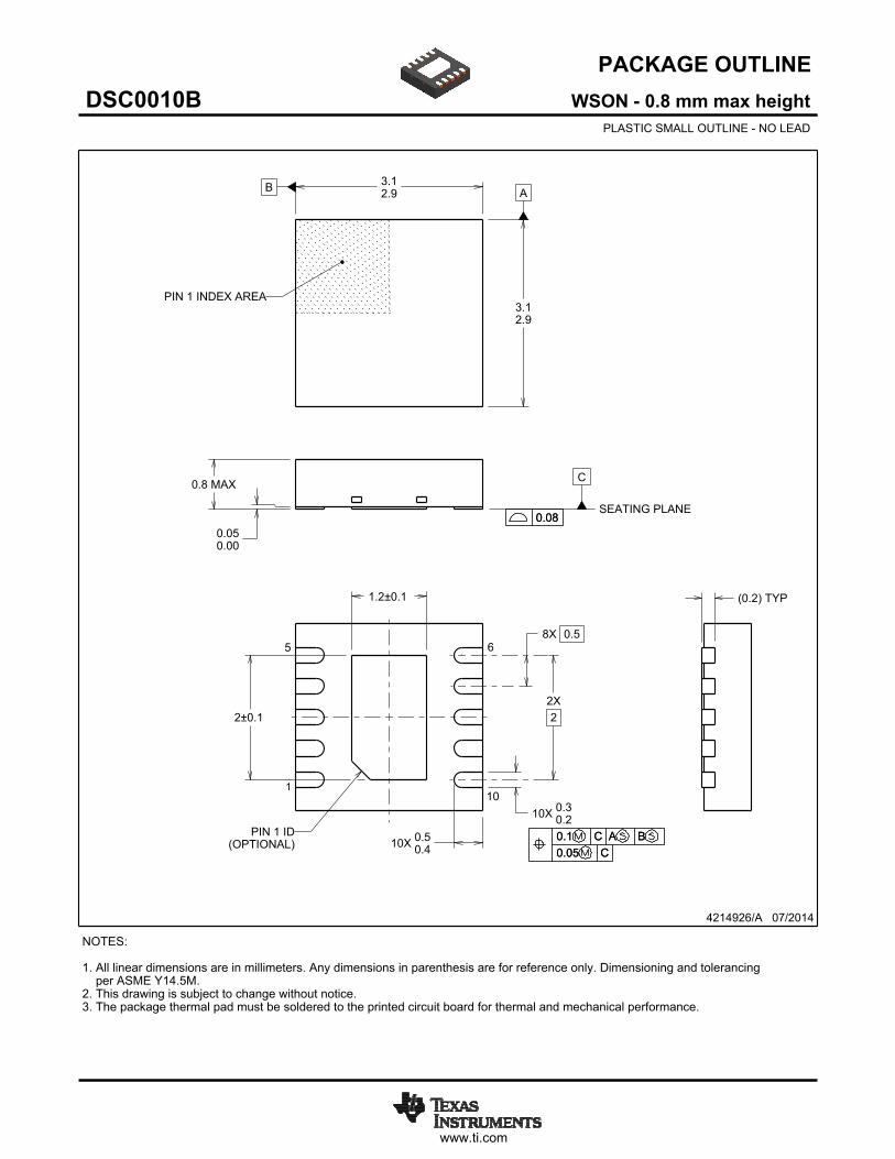
PACKAGE OUTLINE
C
1.2±0.1
10X 0.30.2
10X 0.50.4
0.8 MAX
0.050.00
2±0.12X2
8X 0.5
A
3.12.9
B 3.12.9
(0.2) TYP
WSON - 0.8 mm max heightDSC0010BPLASTIC SMALL OUTLINE - NO LEAD
4214926/A 07/2014
PIN 1 INDEX AREA
0.08SEATING PLANE
(OPTIONAL)PIN 1 ID
1
6
10
5
0.1 C A B0.05 C
NOTES: 1. All linear dimensions are in millimeters. Any dimensions in parenthesis are for reference only. Dimensioning and tolerancing per ASME Y14.5M.2. This drawing is subject to change without notice.3. The package thermal pad must be soldered to the printed circuit board for thermal and mechanical performance.
0.08
0.1 C A B0.05 C
SCALE 4.000
www.ti.com
EXAMPLE BOARD LAYOUT
0.07 MINALL AROUND
0.07 MAXALL AROUND
(1.2)
(2)
10X (0.65)
10X (0.25)
(0.35) TYP
(0.75) TYP
(2.75)
( ) TYPVIA
0.2
8X (0.5)
WSON - 0.8 mm max heightDSC0010BPLASTIC SMALL OUTLINE - NO LEAD
4214926/A 07/2014
SYMM
SYMM
LAND PATTERN EXAMPLESCALE:20X
1
5 6
10
NOTES: (continued) 4. This package is designed to be soldered to a thermal pad on the board. For more information, see Texas Instruments literature number SLUA271 (www.ti.com/lit/slua271).
SOLDER MASKOPENING
METALUNDERSOLDER MASK
SOLDER MASKDEFINED
METALSOLDER MASKOPENING
SOLDER MASK DETAILS
NON SOLDER MASKDEFINED
(PREFERRED)
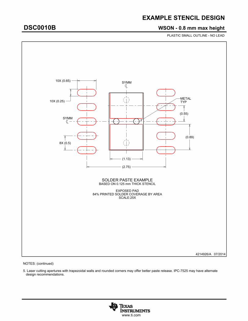
www.ti.com
EXAMPLE STENCIL DESIGN
(1.13)
(0.89)
10X (0.65)
10X (0.25)
8X (0.5)
(2.75)
(0.55)
WSON - 0.8 mm max heightDSC0010BPLASTIC SMALL OUTLINE - NO LEAD
4214926/A 07/2014
NOTES: (continued) 5. Laser cutting apertures with trapezoidal walls and rounded corners may offer better paste release. IPC-7525 may have alternate design recommendations.
SYMM
SYMM
METALTYP
SOLDER PASTE EXAMPLEBASED ON 0.125 mm THICK STENCIL
EXPOSED PAD
84% PRINTED SOLDER COVERAGE BY AREASCALE:25X

IMPORTANT NOTICE AND DISCLAIMERTI PROVIDES TECHNICAL AND RELIABILITY DATA (INCLUDING DATASHEETS), DESIGN RESOURCES (INCLUDING REFERENCEDESIGNS), APPLICATION OR OTHER DESIGN ADVICE, WEB TOOLS, SAFETY INFORMATION, AND OTHER RESOURCES “AS IS”AND WITH ALL FAULTS, AND DISCLAIMS ALL WARRANTIES, EXPRESS AND IMPLIED, INCLUDING WITHOUT LIMITATION ANYIMPLIED WARRANTIES OF MERCHANTABILITY, FITNESS FOR A PARTICULAR PURPOSE OR NON-INFRINGEMENT OF THIRDPARTY INTELLECTUAL PROPERTY RIGHTS.These resources are intended for skilled developers designing with TI products. You are solely responsible for (1) selecting the appropriateTI products for your application, (2) designing, validating and testing your application, and (3) ensuring your application meets applicablestandards, and any other safety, security, or other requirements. These resources are subject to change without notice. TI grants youpermission to use these resources only for development of an application that uses the TI products described in the resource. Otherreproduction and display of these resources is prohibited. No license is granted to any other TI intellectual property right or to any third partyintellectual property right. TI disclaims responsibility for, and you will fully indemnify TI and its representatives against, any claims, damages,costs, losses, and liabilities arising out of your use of these resources.TI’s products are provided subject to TI’s Terms of Sale (https:www.ti.com/legal/termsofsale.html) or other applicable terms available eitheron ti.com or provided in conjunction with such TI products. TI’s provision of these resources does not expand or otherwise alter TI’sapplicable warranties or warranty disclaimers for TI products.IMPORTANT NOTICE
Mailing Address: Texas Instruments, Post Office Box 655303, Dallas, Texas 75265Copyright © 2021, Texas Instruments Incorporated