Embed Size (px)
Citation preview
LTC3440
13440fd
For more information www.linear.com/LTC3440
Description
Micropower Synchronous Buck-Boost DC/DC Converter
Features
applications
n Single Inductor n Fixed Frequency Operation with Battery Voltages
Above, Below or Equal to the Output n Synchronous Rectification: Up to 96% Efficiency n 25µA Quiescent Current in Burst Mode® Operation n Up to 600mA Continuous Output Current n No Schottky Diodes Required (VOUT < 4.3V) n VOUT Disconnected from VIN During Shutdown n 2.5V to 5.5V Input and Output Range n Programmable Oscillator Frequency
from 300kHz to 2MHz n Synchronizable Oscillator n Burst Mode Enable Control n <1µA Shutdown Current n Small Thermally Enhanced 10-Pin MSOP and
(3mm × 3mm) DFN Packages
n Palmtop Computers n Handheld Instruments n MP3 Players n Digital Cameras
The LTC®3440 is a high efficiency, fixed frequency, Buck-Boost DC/DC converter that operates from input voltages above, below or equal to the output voltage. The topology incorporated in the IC provides a continuous transfer function through all operating modes, making the prod-uct ideal for single lithium-ion, multicell alkaline or NiMH applications where the output voltage is within the battery voltage range.
The device includes two 0.19Ω N-channel MOSFET switches and two 0.22Ω P-channel switches. Switch-ing frequencies up to 2MHz are programmed with an external resistor and the oscillator can be synchronized to an external clock. Quiescent current is only 25µA in Burst Mode operation, maximizing battery life in portable applications. Burst Mode operation is user controlled and can be enabled by driving the MODE/SYNC pin high. If the MODE/SYNC pin has either a clock or is driven low, then fixed frequency switching is enabled.
Other features include a 1µA shutdown, soft-start con-trol, thermal shutdown and current limit. The LTC3440 is available in the 10-pin thermally enhanced MSOP and (3mm × 3mm) DFN packages.
Efficiency vs V IN
SW1
VIN
SHDN/SS
MODE/SYNC
RT
SW2
VOUT
FB
VC
GND
3
7
8
2
1
4
6
9
10
5
LTC3440
L110µH
R1340k
R2200k
R315k
3440 TA01
RT60.4k
C1: TAIYO YUDEN JMK212BJ106MGC2: TAIYO YUDEN JMK325BJ226MML1: SUMIDA CDRH6D38-100
*1 = Burst Mode OPERATION 0 = FIXED FREQUENCY
C110µF
Li-Ion
VIN = 2.7V TO 4.2V
*+C5 1.5nF C2
22µF
VOUT3.3V600mA
VIN (V)2.5
EFFI
CIEN
CY (%
)
3.0 3.5 4.0 4.5
3440 TA02
5.0
100
98
96
94
92
90
88
86
84
82
805.5
VOUT = 3.3VIOUT = 100mAfOSC = 1MHz
typical applicationLi-Ion to 3.3V at 600mA Buck-Boost Converter
L, LT, LTC, LTM, Linear Technology, Burst Mode and the Linear logo are registered trademarks and ThinSOT is a trademark of Linear Technology Corporation. All other trademarks are the property of their respective owners.
LTC3440
23440fd
For more information www.linear.com/LTC3440
absolute MaxiMuM ratingsVIN, VOUT Voltage ....................................... –0.3V to 6VSW1, SW2 Voltage ...................................... –0.3V to 6VVC, RT, FB, SHDN/SS, MODE/SYNC Voltage .................................. –0.3V to 6V
The ● denotes specifications that apply over the full operating temperature range, otherwise specifications are at TA = 25°C. VIN = VOUT = 3.6V, RT = 60k, unless otherwise noted.
Operating Temperature Range (Note 2)....–40°C to 85°CStorage Temperature Range .................. –65°C to 125°CLead Temperature (Soldering, 10 sec) ................... 300°C
electrical characteristics
PARAMETER CONDITIONS MIN TYP MAX UNITS
Input Start-Up Voltage l 2.4 2.5 V
Input Operating Range l 2.5 5.5 V
Output Voltage Adjust Range l 2.5 5.5 V
Feedback Voltage l 1.196 1.22 1.244 V
Feedback Input Current VFB = 1.22V 1 50 nA
Quiescent Current, Burst Mode Operation VC = 0V, MODE/SYNC = 3V (Note 3) 25 40 µA
Quiescent Current, Shutdown SHDN = 0V, Not Including Switch Leakage 0.1 1 µA
Quiescent Current, Active VC = 0V, MODE/SYNC = 0V (Note 3) 600 1000 µA
NMOS Switch Leakage Switches B and C 0.1 5 µA
pin conFiguration
TOP VIEW
DD PACKAGE10-LEAD (3mm × 3mm) PLASTIC DFN
EXPOSED PAD (PIN 11) IS GNDMUST BE SOLDERED TO PCB
10
9
6
7
8
4
5
3
2
1 VC
FB
SHDN/SS
VIN
VOUT
RT
MODE/SYNC
SW1
SW2
GND
11
TJMAX = 125°C, θJA = 43°C/W, θJC = 3°C/W
12345
RTMODE/SYNC
SW1SW2GND
109876
VCFBSHDN/SSVINVOUT
TOP VIEW
MS PACKAGE10-LEAD PLASTIC MSOP
TJMAX = 125°C, θJA = 130°C/W 1 LAYER BOARDθJA = 100°C/W 4 LAYER BOARD
θJC = 45°C/W
orDer inForMationLEAD FREE FINISH TAPE AND REEL PART MARKING PACKAGE DESCRIPTION TEMPERATURE RANGE
LTC3440EDD#PBF LTC3440EDD#TRPBF LBKT 10-Lead (3mm × 3mm) Plastic DFN –40°C to 85°C
LTC3440EMS#PBF LTC3440EMS#TRPBF LTNP 10-Lead Plastic MSOP –40°C to 85°C
Consult LTC Marketing for parts specified with wider operating temperature ranges. Consult LTC Marketing for information on nonstandard lead based finish parts.For more information on lead free part marking, go to: http://www.linear.com/leadfree/ For more information on tape and reel specifications, go to: http://www.linear.com/tapeandreel/. Some packages are available in 500 unit reels through designated sales channels with #TRMPBF suffix.
(Note 1)
http://www.linear.com/product/LTC3440#orderinfo
LTC3440
33440fd
For more information www.linear.com/LTC3440
PARAMETER CONDITIONS MIN TYP MAX UNITS
PMOS Switch Leakage Switches A and D 0.1 10 µA
NMOS Switch On Resistance Switches B and C 0.19 Ω
PMOS Switch On Resistance Switches A and D 0.22 Ω
Input Current Limit l 1 A
Maximum Duty Cycle Boost (% Switch C On) Buck (% Switch A On)
l
l
55 100
75 % %
Minimum Duty Cycle l 0 %
Frequency Accuracy l 0.8 1 1.2 MHz
MODE/SYNC Threshold 0.4 2 V
MODE/SYNC Input Current VMODE/SYNC = 5.5V 0.01 1 µA
Error Amp AVOL 90 dB
Error Amp Source Current 15 µA
Error Amp Sink Current 380 µA
SHDN/SS Threshold When IC is Enabled When EA is at Maximum Boost Duty Cycle
l 0.4 1 2.2
1.5 V V
SHDN/SS Input Current VSHDN = 5.5V 0.01 1 µA
The ● denotes specifications that apply over the full operating temperature range, otherwise specifications are at TA = 25°C. VIN = VOUT = 3.6V, RT = 60k, unless otherwise noted.electrical characteristics
Note 1: Absolute Maximum Ratings are those values beyond which the life of the device may be impaired. Note 2: The LTC3440E is guaranteed to meet performance specifications from 0°C to 70°C. Specifications over the –40°C to 85°C operating
temperature range are assured by design, characterization and correlation with statistical process controls. Note 3: Current measurements are performed when the outputs are not switching.
typical perForMance characteristics
Li-Ion to 3.3V Efficiency (fOSC = 300kHz)
OUTPUT CURRENT (mA)
30
EFFI
CIEN
CY (%
)
90
100
20
80
50
70
60
40
0.1 10 100 1000
3440 G02
1
Burst ModeOPERATION
VIN = 3.3VVIN = 2.5V
POWER LOSS (m
W)
VIN = 4.2V
0.1
1
10
100
1000
fOSC = 1MHz
VIN = 3.3V
OUTPUT CURRENT (mA)
30
EFFI
CIEN
CY (%
)
90
100
20
80
50
70
60
40
0.1 10 100 1000
3440 G03
1
Burst ModeOPERATION
VIN = 2.5V
VIN = 3.3V
fOSC = 2MHz
VIN = 4.2V
Li-Ion to 3.3V Efficiency, Power Loss (fOSC = 1MHz)
Li-Ion to 3.3V Efficiency(fOSC = 2MHz)
OUTPUT CURRENT (mA)
30
EFFI
CIEN
CY (%
)
90
100
20
80
50
70
60
40
0.1 10 100 1000
3440 G01
1
Burst ModeOPERATION
VIN = 2.5V VIN = 3.3V
fOSC = 300kHz
VIN = 4.2V
LTC3440
43440fd
For more information www.linear.com/LTC3440
typical perForMance characteristics
Active Quiescent Current Burst Mode Quiescent Current Error Amp Source Current
TEMPERATURE (°C)–55
400
V IN
+ V O
UT C
URRE
NT (µ
A)
450
500
550
–25 5 35 65
3440 G10
95 125
VIN = VOUT = 3.6V
Switch Pins in Buck ModeVOUT Ripple During Buck, Buck/Boost and Boost ModesSwitch Pins in Boost Mode
250ns/DIVVIN = 5VVOUT = 3.3VIOUT = 250mA
SW22V/DIV
SW12V/DIV
3440 G07 250ns/DIVVIN = 2.5VVOUT = 3.3VIOUT = 250mA
SW22V/DIV
SW12V/DIV
3440 G08 1µs/DIVL = 10µHCOUT = 22µFIOUT = 250mAfOSC = 1MHz
BuckVIN = 5V
Buck/BoostVIN = 3.78V
BoostVIN = 2.5V
VOUT10mV/DIV
AC Coupled
3440 G09
Switch Pins During Buck/BoostSwitch Pins on the Edge of Buck/Boost and Approaching Boost
Switch Pins on the Edge of Buck/Boost and Approaching Buck
50ns/DIVVIN = 3.78VVOUT = 3.3VIOUT = 250mA
SW22V/DIV
SW12V/DIV
3440 G04 50ns/DIVVIN = 3.42VVOUT = 3.3VIOUT = 250mA
SW22V/DIV
SW12V/DIV
3440 G05 50ns/DIVVIN = 4.15VVOUT = 3.3VIOUT = 250mA
SW22V/DIV
SW12V/DIV
3440 G06
TEMPERATURE (°C)–55
10
V IN
+ V O
UT C
URRE
NT (µ
A)
20
30
40
–25 5 35 65
3440 G11
95 125
VIN = VOUT = 3.6V
TEMPERATURE (°C)–55
5
E/A
SOUR
CE C
URRE
NT (µ
A)
10
15
20
–25 5 35 65
3440 G12
95 125
VIN = VOUT = 3.6V
LTC3440
53440fd
For more information www.linear.com/LTC3440
typical perForMance characteristics
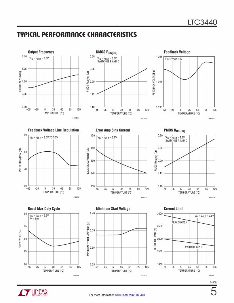
Output Frequency NMOS RDS(ON) Feedback Voltage
TEMPERATURE (°C)–55
0.90
FREQ
UENC
Y (M
Hz)
0.95
1.00
1.05
1.10
–25 5 35 65
3440 G13
95 125
VIN = VOUT = 3.6V
TEMPERATURE (°C)–55
0.10
NMOS
RDS
(ON)
(Ω)
0.15
0.20
0.25
0.30
–25 5 35 65
3440 G14
95 125
VIN = VOUT = 3.6VSWITCHES B AND C
TEMPERATURE (°C)–55
1.196
FEED
BACK
VOL
TAGE
(V)
1.216
1.236
–25 5 35 65
3440 G15
95 125
VIN = VOUT = 3V
Boost Max Duty Cycle Minimum Start Voltage Current Limit
TEMPERATURE (°C)–55
70
DUTY
CYC
LE (%
)
75
80
85
90
–25 5 35 65
3440 G19
95 125
VIN = VOUT = 3.6VRT = 60k
TEMPERATURE (°C)–55
2.25
MIN
IMUM
STA
RT V
OLTA
GE (V
)
2.30
2.35
2.40
–25 5 35 65
3440 G20
95 125TEMPERATURE (°C)
–551000
CURR
ENT
LIM
IT (A
)
1500
2000
2500
3000
–25 5 35 65
3440 G21
95 125
VIN = VOUT = 3.6V
PEAK SWITCH
AVERAGE INPUT
Feedback Voltage Line Regulation Error Amp Sink Current PMOS RDS(ON)
TEMPERATURE (°C)–55
60
LINE
REG
ULAT
ION
(dB)
70
80
90
–25 5 35 65
3440 G16
95 125
VIN = VOUT = 2.5V TO 5.5V
TEMPERATURE (°C)–55
350
E/A
SINK
CUR
RENT
(µA)
370
390
410
430
–25 5 35 65
3440 G17
95 125
VIN = VOUT = 3.6V
TEMPERATURE (°C)–55
0.10
PMOS
RDS
(ON)
(Ω)
0.15
0.20
0.25
0.30
–25 5 35 65
3440 G18
95 125
VIN = VOUT = 3.6VSWITCHES A AND D
LTC3440
63440fd
For more information www.linear.com/LTC3440
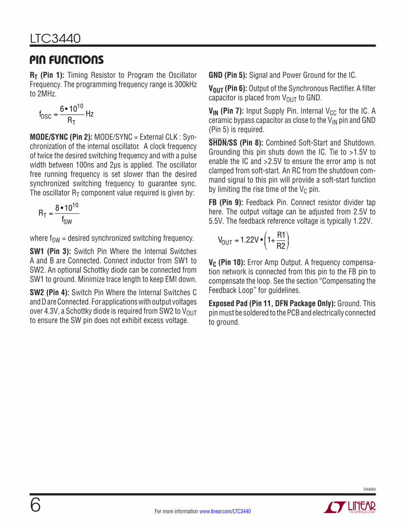
pin FunctionsRT (Pin 1): Timing Resistor to Program the Oscillator Frequency. The programming frequency range is 300kHz to 2MHz.
fOSC =
6 • 1010
RTHz
MODE/SYNC (Pin 2): MODE/SYNC = External CLK : Syn-chronization of the internal oscillator. A clock frequency of twice the desired switching frequency and with a pulse width between 100ns and 2µs is applied. The oscillator free running frequency is set slower than the desired synchronized switching frequency to guarantee sync. The oscillator RT component value required is given by:
RT =
8 •1010
fSW
where fSW = desired synchronized switching frequency.
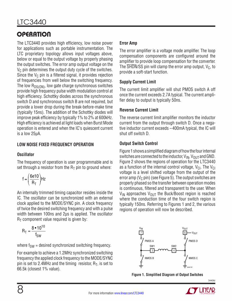
SW1 (Pin 3): Switch Pin Where the Internal Switches A and B are Connected. Connect inductor from SW1 to SW2. An optional Schottky diode can be connected from SW1 to ground. Minimize trace length to keep EMI down.
SW2 (Pin 4): Switch Pin Where the Internal Switches C and D are Connected. For applications with output voltages over 4.3V, a Schottky diode is required from SW2 to VOUT to ensure the SW pin does not exhibit excess voltage.
GND (Pin 5): Signal and Power Ground for the IC.
VOUT (Pin 6): Output of the Synchronous Rectifier. A filter capacitor is placed from VOUT to GND.
VIN (Pin 7): Input Supply Pin. Internal VCC for the IC. A ceramic bypass capacitor as close to the VIN pin and GND (Pin 5) is required.
SHDN/SS (Pin 8): Combined Soft-Start and Shutdown. Grounding this pin shuts down the IC. Tie to >1.5V to enable the IC and >2.5V to ensure the error amp is not clamped from soft-start. An RC from the shutdown com-mand signal to this pin will provide a soft-start function by limiting the rise time of the VC pin.
FB (Pin 9): Feedback Pin. Connect resistor divider tap here. The output voltage can be adjusted from 2.5V to 5.5V. The feedback reference voltage is typically 1.22V.
VOUT = 1.22V • 1+
R1R2
⎛
⎝⎜
⎞
⎠⎟
VC (Pin 10): Error Amp Output. A frequency compensa-tion network is connected from this pin to the FB pin to compensate the loop. See the section “Compensating the Feedback Loop” for guidelines.
Exposed Pad (Pin 11, DFN Package Only): Ground. This pin must be soldered to the PCB and electrically connected to ground.
LTC3440
73440fd
For more information www.linear.com/LTC3440
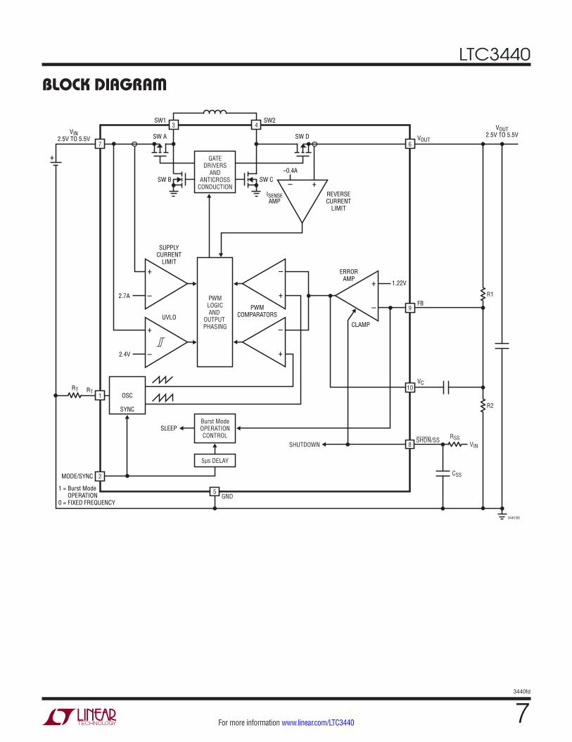
block DiagraM
–
+
– +
–
+
–
+
–
+
–
+
7
PWMLOGICAND
OUTPUT PHASING
GATEDRIVERS
ANDANTICROSS
CONDUCTION
Burst ModeOPERATIONCONTROL
5µs DELAY
GND
UVLO
2.7A
2.4V
RT
SLEEP
MODE/SYNC
1 = Burst Mode OPERATION0 = FIXED FREQUENCY
RTOSC
SYNC
SUPPLYCURRENT
LIMIT
SW A
SW1 SW2
VIN2.5V TO 5.5V SW D
ISENSEAMP
ERRORAMP
1.22V
CLAMP
REVERSECURRENT
LIMIT
SW B SW C–0.4A
1
2
5
8
+
3 4
VOUT6
FB9
VC10
SHDN/SSSHUTDOWN
RSSVIN
R2
CSS
R1
3440 BD
VOUT2.5V TO 5.5V
PWMCOMPARATORS
LTC3440
83440fd
For more information www.linear.com/LTC3440
operationThe LTC3440 provides high efficiency, low noise power for applications such as portable instrumentation. The LTC proprietary topology allows input voltages above, below or equal to the output voltage by properly phasing the output switches. The error amp output voltage on the VC pin determines the output duty cycle of the switches. Since the VC pin is a filtered signal, it provides rejection of frequencies from well below the switching frequency. The low RDS(ON), low gate charge synchronous switches provide high frequency pulse width modulation control at high efficiency. Schottky diodes across the synchronous switch D and synchronous switch B are not required, but provide a lower drop during the break-before-make time (typically 15ns). The addition of the Schottky diodes will improve peak efficiency by typically 1% to 2% at 600kHz. High efficiency is achieved at light loads when Burst Mode operation is entered and when the IC’s quiescent current is a low 25µA.
LOW NOISE FIXED FREQUENCY OPERATION
Oscillator
The frequency of operation is user programmable and is set through a resistor from the RT pin to ground where:
f =
6e10RT
⎛
⎝⎜
⎞
⎠⎟Hz
An internally trimmed timing capacitor resides inside the IC. The oscillator can be synchronized with an external clock applied to the MODE/SYNC pin. A clock frequency of twice the desired switching frequency and with a pulse width between 100ns and 2µs is applied. The oscillator RT component value required is given by:
RT =
8 •1010
fSW
where fSW = desired synchronized switching frequency.
For example to achieve a 1.2MHz synchronized switching frequency the applied clock frequency to the MODE/SYNC pin is set to 2.4MHz and the timing resistor, RT, is set to 66.5k (closest 1% value).
Error Amp
The error amplifier is a voltage mode amplifier. The loop compensation components are configured around the amplifier to provide loop compensation for the converter. The SHDN/SS pin will clamp the error amp output, VC, to provide a soft-start function.
Supply Current Limit
The current limit amplifier will shut PMOS switch A off once the current exceeds 2.7A typical. The current ampli-fier delay to output is typically 50ns.
Reverse Current Limit
The reverse current limit amplifier monitors the inductor current from the output through switch D. Once a nega-tive inductor current exceeds –400mA typical, the IC will shut off switch D.
Output Switch Control
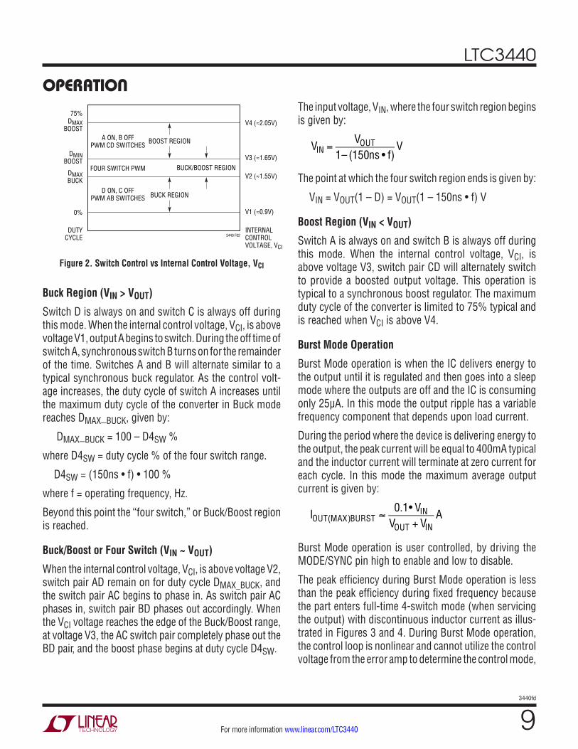
Figure 1 shows a simplified diagram of how the four internal switches are connected to the inductor, VIN, VOUT and GND. Figure 2 shows the regions of operation for the LTC3440 as a function of the internal control voltage, VCI. The VCI voltage is a level shifted voltage from the output of the error amp (VC pin) (see Figure 5). The output switches are properly phased so the transfer between operation modes is continuous, filtered and transparent to the user. When VIN approaches VOUT the Buck/Boost region is reached where the conduction time of the four switch region is typically 150ns. Referring to Figures 1 and 2, the various regions of operation will now be described.
Figure 1. Simplified Diagram of Output Switches
3
SW1
4
SW2
PMOS A
NMOS B
7
VIN
PMOS D
NMOS C
3440 F01
6
VOUT
VOUT
LTC3440
93440fd
For more information www.linear.com/LTC3440
Buck Region (VIN > VOUT)
Switch D is always on and switch C is always off during this mode. When the internal control voltage, VCI, is above voltage V1, output A begins to switch. During the off time of switch A, synchronous switch B turns on for the remainder of the time. Switches A and B will alternate similar to a typical synchronous buck regulator. As the control volt-age increases, the duty cycle of switch A increases until the maximum duty cycle of the converter in Buck mode reaches DMAX_BUCK, given by:
DMAX_BUCK = 100 – D4SW %
where D4SW = duty cycle % of the four switch range.
D4SW = (150ns • f) • 100 %
where f = operating frequency, Hz.
Beyond this point the “four switch,” or Buck/Boost region is reached.
Buck/Boost or Four Switch (VIN ~ VOUT)
When the internal control voltage, VCI, is above voltage V2, switch pair AD remain on for duty cycle DMAX_BUCK, and the switch pair AC begins to phase in. As switch pair AC phases in, switch pair BD phases out accordingly. When the VCI voltage reaches the edge of the Buck/Boost range, at voltage V3, the AC switch pair completely phase out the BD pair, and the boost phase begins at duty cycle D4SW.
Figure 2. Switch Control vs Internal Control Voltage, VCI
The input voltage, VIN, where the four switch region begins is given by:
VIN =
VOUT1– (150ns • f)
V
The point at which the four switch region ends is given by:
VIN = VOUT(1 – D) = VOUT(1 – 150ns • f) V
Boost Region (VIN < VOUT)
Switch A is always on and switch B is always off during this mode. When the internal control voltage, VCI, is above voltage V3, switch pair CD will alternately switch to provide a boosted output voltage. This operation is typical to a synchronous boost regulator. The maximum duty cycle of the converter is limited to 75% typical and is reached when VCI is above V4.
Burst Mode Operation
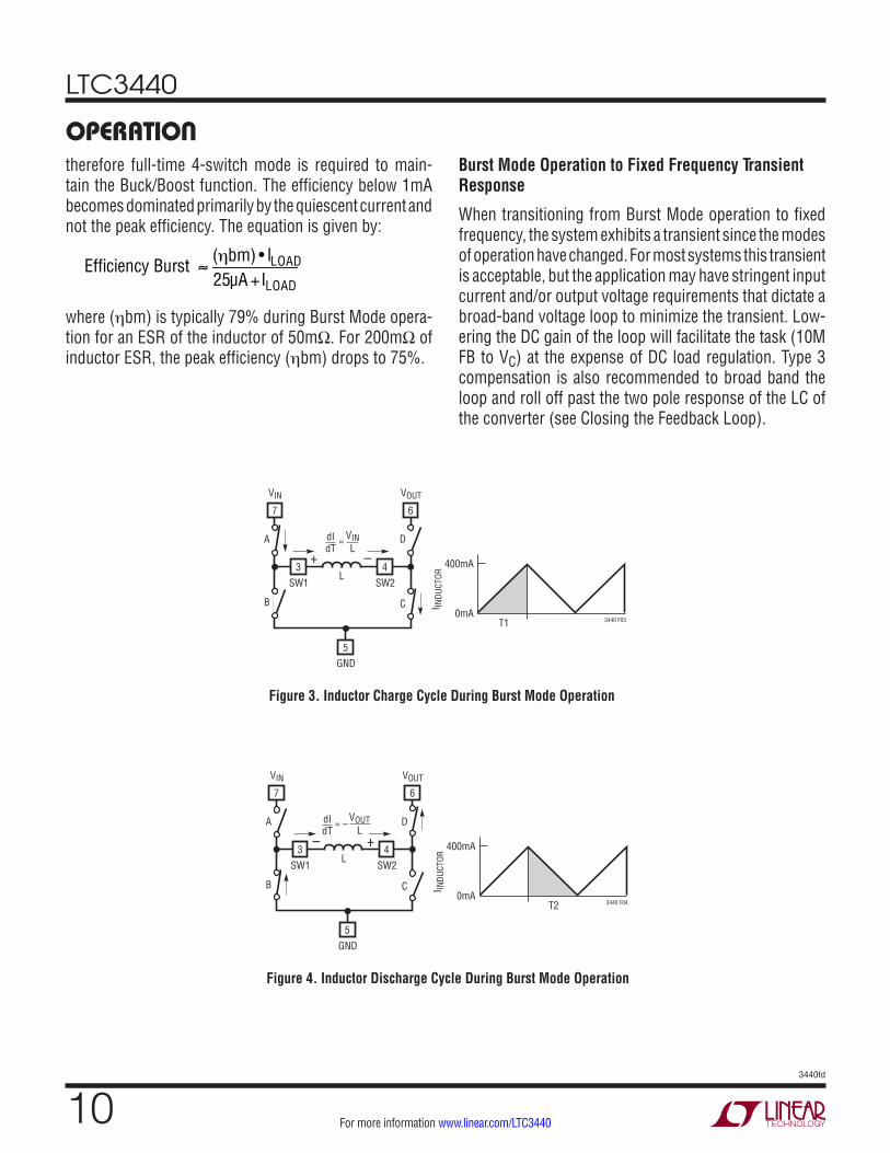
Burst Mode operation is when the IC delivers energy to the output until it is regulated and then goes into a sleep mode where the outputs are off and the IC is consuming only 25µA. In this mode the output ripple has a variable frequency component that depends upon load current.
During the period where the device is delivering energy to the output, the peak current will be equal to 400mA typical and the inductor current will terminate at zero current for each cycle. In this mode the maximum average output current is given by:
IOUT(MAX)BURST ≈
0.1• VINVOUT + VIN
A
Burst Mode operation is user controlled, by driving the MODE/SYNC pin high to enable and low to disable.
The peak efficiency during Burst Mode operation is less than the peak efficiency during fixed frequency because the part enters full-time 4-switch mode (when servicing the output) with discontinuous inductor current as illus-trated in Figures 3 and 4. During Burst Mode operation, the control loop is nonlinear and cannot utilize the control voltage from the error amp to determine the control mode,
75%DMAX
BOOST
DMINBOOST
DMAXBUCK
DUTYCYCLE
0%
V4 (≈2.05V)
V3 (≈1.65V)
BOOST REGION
BUCK REGION
BUCK/BOOST REGIONV2 (≈1.55V)
V1 (≈0.9V)
3440 F02
A ON, B OFFPWM CD SWITCHES
D ON, C OFFPWM AB SWITCHES
FOUR SWITCH PWM
INTERNALCONTROLVOLTAGE, VCI
operation
LTC3440
103440fd
For more information www.linear.com/LTC3440
therefore full-time 4-switch mode is required to main-tain the Buck/Boost function. The efficiency below 1mA becomes dominated primarily by the quiescent current and not the peak efficiency. The equation is given by:
Efficiency Burst ≈
(ηbm) • ILOAD25µA +ILOAD
where (ηbm) is typically 79% during Burst Mode opera-tion for an ESR of the inductor of 50mΩ. For 200mΩ of inductor ESR, the peak efficiency (ηbm) drops to 75%.
Burst Mode Operation to Fixed Frequency Transient Response
When transitioning from Burst Mode operation to fixed frequency, the system exhibits a transient since the modes of operation have changed. For most systems this transient is acceptable, but the application may have stringent input current and/or output voltage requirements that dictate a broad-band voltage loop to minimize the transient. Low-ering the DC gain of the loop will facilitate the task (10M FB to VC) at the expense of DC load regulation. Type 3 compensation is also recommended to broad band the loop and roll off past the two pole response of the LC of the converter (see Closing the Feedback Loop).
7
VIN
A
3SW1
5GND
4SW2
L
+ –
6
VOUT
D
C
400mA
I INDU
CTOR
0mA3440 F03T1
B
dIdT
VINL
≈
7
VIN
A
3SW1
5GND
4SW2
L
– +
6
VOUT
D
C
400mA
I INDU
CTOR
0mA3440 F04T2
B
dIdT
VOUTL
≈ –
Figure 3. Inductor Charge Cycle During Burst Mode Operation
Figure 4. Inductor Discharge Cycle During Burst Mode Operation
operation
LTC3440
113440fd
For more information www.linear.com/LTC3440
operationSOFT-START
The soft-start function is combined with shutdown. When the SHDN/SS pin is brought above typically 1V, the IC is enabled but the EA duty cycle is clamped from
Figure 5. Soft-Start Circuitry
–
+
9
10
VINERROR AMP
1.22V
15µA
FB R1
R2CP1VC
VOUT
8
SHDN/SS
CSS
1V
ENABLE SIGNALRSS
SOFT-STARTCLAMP
TO PWMCOMPARATORS
CHIPENABLE
3440 F05
–
+
VCI
the VC pin. A detailed diagram of this function is shown in Figure 5. The components RSS and CSS provide a slow ramping voltage on the SHDN/SS pin to provide a soft-start function.
LTC3440
123440fd
For more information www.linear.com/LTC3440
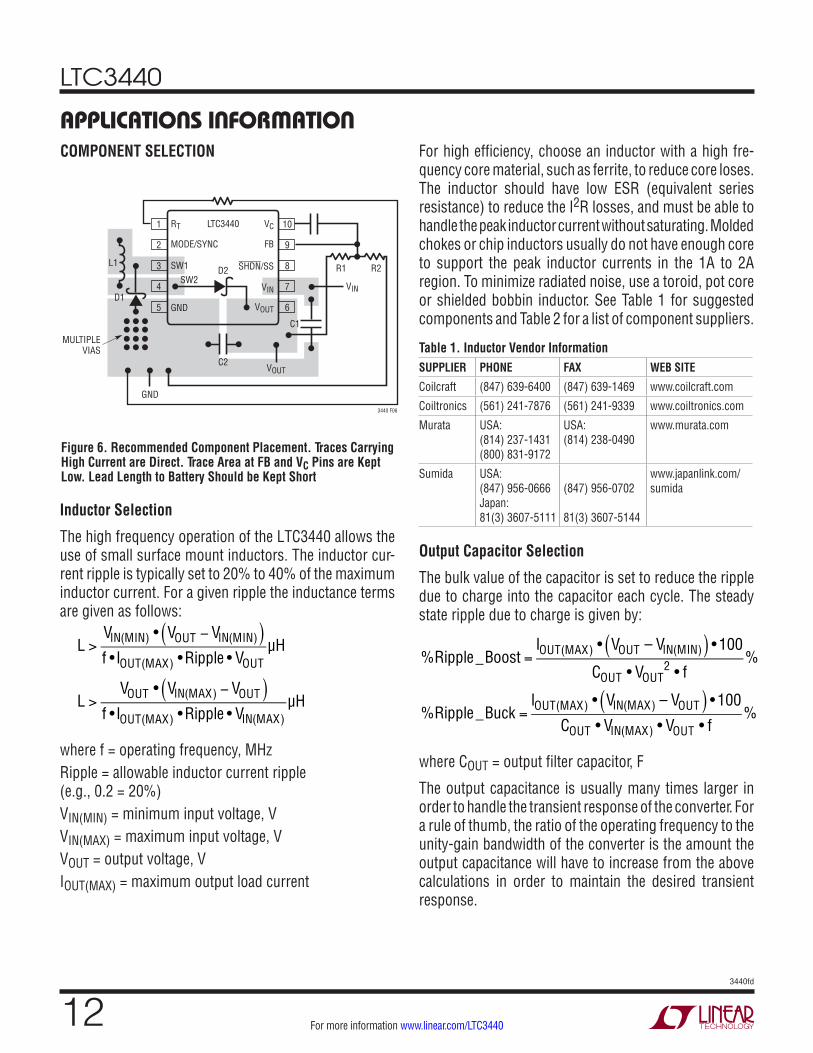
COMPONENT SELECTION
Inductor Selection
The high frequency operation of the LTC3440 allows the use of small surface mount inductors. The inductor cur-rent ripple is typically set to 20% to 40% of the maximum inductor current. For a given ripple the inductance terms are given as follows:
L >VIN(MIN) • VOUT − VIN(MIN)( )f • IOUT(MAX) •Ripple • VOUT
µH
L >VOUT • VIN(MAX) − VOUT( )
f • IOUT(MAX) •Ripple • VIN(MAX)µH
where f = operating frequency, MHzRipple = allowable inductor current ripple (e.g., 0.2 = 20%)VIN(MIN) = minimum input voltage, VVIN(MAX) = maximum input voltage, VVOUT = output voltage, VIOUT(MAX) = maximum output load current
3440 F06
GND
C2
D2
LTC3440
MULTIPLEVIAS
L1
RT VC
FB
SHDN/SS
VIN
VOUT
MODE/SYNC
SW1
GND
SW2
D1VIN
R1 R2
VOUT
C1
1
2
3
4
5
10
9
8
7
6
applications inForMation
Figure 6. Recommended Component Placement. Traces Carrying High Current are Direct. Trace Area at FB and VC Pins are Kept Low. Lead Length to Battery Should be Kept Short
For high efficiency, choose an inductor with a high fre-quency core material, such as ferrite, to reduce core loses. The inductor should have low ESR (equivalent series resistance) to reduce the I2R losses, and must be able to handle the peak inductor current without saturating. Molded chokes or chip inductors usually do not have enough core to support the peak inductor currents in the 1A to 2A region. To minimize radiated noise, use a toroid, pot core or shielded bobbin inductor. See Table 1 for suggested components and Table 2 for a list of component suppliers.
Table 1. Inductor Vendor InformationSUPPLIER PHONE FAX WEB SITE
Coilcraft (847) 639-6400 (847) 639-1469 www.coilcraft.com
Coiltronics (561) 241-7876 (561) 241-9339 www.coiltronics.com
Murata USA: (814) 237-1431 (800) 831-9172
USA: (814) 238-0490
www.murata.com
Sumida USA: (847) 956-0666 Japan: 81(3) 3607-5111
(847) 956-0702 81(3) 3607-5144
www.japanlink.com/ sumida
Output Capacitor Selection
The bulk value of the capacitor is set to reduce the ripple due to charge into the capacitor each cycle. The steady state ripple due to charge is given by:
%Ripple_Boost =IOUT(MAX) • VOUT – VIN(MIN)( ) •100
COUT • VOUT2 • f
%
%Ripple_Buck =IOUT(MAX) • VIN(MAX) – VOUT( ) •100
COUT • VIN(MAX) • VOUT • f%
where COUT = output filter capacitor, F
The output capacitance is usually many times larger in order to handle the transient response of the converter. For a rule of thumb, the ratio of the operating frequency to the unity-gain bandwidth of the converter is the amount the output capacitance will have to increase from the above calculations in order to maintain the desired transient response.
LTC3440
133440fd
For more information www.linear.com/LTC3440
applications inForMationInput Voltage > 4.5V
For applications with input voltages above 4.5V which could exhibit an overload or short-circuit condition, a 2Ω/1nF series snubber is required between the SW1 pin and GND. A Schottky diode such as the Phillips PMEG2010EA or equivalent from SW1 to VIN should also be added as close to the pins as possible. For the higher input voltages VIN bypassing becomes more critical, therefore, a ceramic bypass capacitor as close to the VIN and GND pins as possible is also required.
Operating Frequency Selection
There are several considerations in selecting the operat-ing frequency of the converter. The first is, what are the sensitive frequency bands that cannot tolerate any spec-tral noise? For example, in products incorporating RF communications, the 455kHz IF frequency is sensitive to any noise, therefore switching above 600kHz is desired. Some communications have sensitivity to 1.1MHz and in that case a 2MHz converter frequency may be employed.
Other considerations are the physical size of the converter and efficiency. As the operating frequency goes up, the inductor and filter capacitors go down in value and size. The trade off is in efficiency since the switching losses due to gate charge are going up proportional with frequency.
Additional quiescent current due to the output switches GATE charge is given by:
Buck: (0.5 • VIN • f ) mA
Boost: [0.25 • (VIN + VOUT) • f ] mA
Buck/Boost: f • (0.75 • VIN + 0.25 • VOUT) mA
where f = switching frequency in MHz
The other component of ripple is due to the ESR (equiva-lent series resistance) of the output capacitor. Low ESR capacitors should be used to minimize output voltage ripple. For surface mount applications, Taiyo Yuden ceramic capacitors, AVX TPS series tantalum capacitors or Sanyo POSCAP are recommended.
Input Capacitor Selection
Since the VIN pin is the supply voltage for the IC it is recommended to place at least a 4.7µF, low ESR bypass capacitor.
Table 2. Capacitor Vendor InformationSUPPLIER PHONE FAX WEB SITE
AVX (803) 448-9411 (803) 448-1943 www.avxcorp.com
Sanyo (619) 661-6322 (619) 661-1055 www.sanyovideo.com
Taiyo Yuden (408) 573-4150 (408) 573-4159 www.t-yuden.com
Optional Schottky Diodes
To achieve a 1%-2% efficiency improvement above 50mW, Schottky diodes can be added across synchronous switches B (SW1 to GND) and D (SW2 to VOUT). The Schottky diodes will provide a lower voltage drop during the break-before-make time (typically 15ns) of the NMOS to PMOS transition. General purpose diodes such as a 1N914 are not recommended due to the slow recovery times and will compromise efficiency. If desired a large Schottky diode, such as an MBRM120T3, can be used from SW2 to VOUT. A low capacitance Schottky diode is recommended from GND to SW1 such as a Phillips PMEG2010EA or equivalent.
Output Voltage > 4.3V
A Schottky diode from SW to VOUT is required for output voltages over 4.3V. The diode must be located as close to the pins as possible in order to reduce the peak voltage on SW2 due to the parasitic lead and trace inductance.
LTC3440
143440fd
For more information www.linear.com/LTC3440
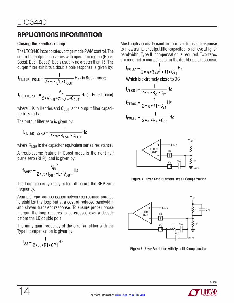
applications inForMationClosing the Feedback Loop
The LTC3440 incorporates voltage mode PWM control. The control to output gain varies with operation region (Buck, Boost, Buck-Boost), but is usually no greater than 15. The output filter exhibits a double pole response is given by:
fFILTER _POLE =
12 • π • L •COUT
Hz(inBuck mode)
fFILTER_POLE =
VIN
2 •VOUT •π • L •COUTHz (inBoost mode)
where L is in Henries and COUT is the output filter capaci-tor in Farads.
The output filter zero is given by:
fFILTER _ ZERO =
12 • π •RESR •COUT
Hz
where RESR is the capacitor equivalent series resistance.
A troublesome feature in Boost mode is the right-half plane zero (RHP), and is given by:
fRHPZ =
VIN2
2 • π • IOUT •L • VOUTHz
The loop gain is typically rolled off before the RHP zero frequency.
A simple Type I compensation network can be incorporated to stabilize the loop but at a cost of reduced bandwidth and slower transient response. To ensure proper phase margin, the loop requires to be crossed over a decade before the LC double pole.
The unity-gain frequency of the error amplifier with the Type I compensation is given by:
fUG =
12 • π •R1•CP1
Hz
Most applications demand an improved transient response to allow a smaller output filter capacitor. To achieve a higher bandwidth, Type III compensation is required. Two zeros are required to compensate for the double-pole response.
fPOLE1 ≈1
2 • π •32e3 •R1• CP1Hz
Which is extremely close to DC
fZERO1=1
2 • π •RZ •CP1Hz
fZERO2 =1
2 • π •R1 •CZ1Hz
fPOLE2 =1
2 • π •RZ •CP2Hz
Figure 8. Error Amplifier with Type III Compensation
1.22VR1
R2
3440 F08
FB
9
VCCP1
CZ1
RZ
VOUT
10CP2
–
+ERROR
AMP
Figure 7. Error Amplifier with Type I Compensation
1.22V
R1
R2
3440 F07
FB
9
VCCP1
VOUT
10
–
+ERROR
AMP
LTC3440
153440fd
For more information www.linear.com/LTC3440
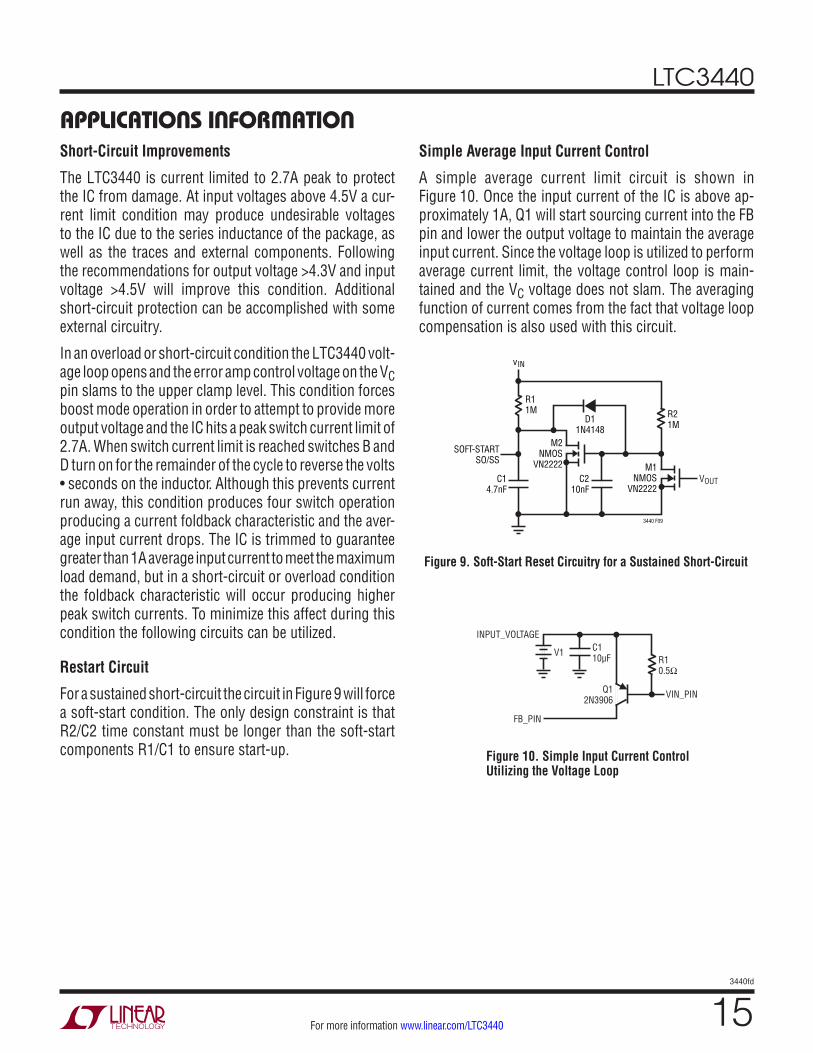
Short-Circuit Improvements
The LTC3440 is current limited to 2.7A peak to protect the IC from damage. At input voltages above 4.5V a cur-rent limit condition may produce undesirable voltages to the IC due to the series inductance of the package, as well as the traces and external components. Following the recommendations for output voltage >4.3V and input voltage >4.5V will improve this condition. Additional short-circuit protection can be accomplished with some external circuitry.
In an overload or short-circuit condition the LTC3440 volt-age loop opens and the error amp control voltage on the VC pin slams to the upper clamp level. This condition forces boost mode operation in order to attempt to provide more output voltage and the IC hits a peak switch current limit of 2.7A. When switch current limit is reached switches B and D turn on for the remainder of the cycle to reverse the volts • seconds on the inductor. Although this prevents current run away, this condition produces four switch operation producing a current foldback characteristic and the aver-age input current drops. The IC is trimmed to guarantee greater than 1A average input current to meet the maximum load demand, but in a short-circuit or overload condition the foldback characteristic will occur producing higher peak switch currents. To minimize this affect during this condition the following circuits can be utilized.
Restart Circuit
For a sustained short-circuit the circuit in Figure 9 will force a soft-start condition. The only design constraint is that R2/C2 time constant must be longer than the soft-start components R1/C1 to ensure start-up.
Simple Average Input Current Control
A simple average current limit circuit is shown in Figure 10. Once the input current of the IC is above ap-proximately 1A, Q1 will start sourcing current into the FB pin and lower the output voltage to maintain the average input current. Since the voltage loop is utilized to perform average current limit, the voltage control loop is main-tained and the VC voltage does not slam. The averaging function of current comes from the fact that voltage loop compensation is also used with this circuit.
Figure 9. Soft-Start Reset Circuitry for a Sustained Short-Circuit
C210nF
C14.7nF
R21M
R11M
VOUT
VIN
SOFT-STARTSO/SS
M2NMOS
VN2222 M1NMOS
VN2222
D11N4148
3440 F09
applications inForMation
Figure 10. Simple Input Current Control Utilizing the Voltage Loop
INPUT_VOLTAGE
FB_PIN
VIN_PINQ12N3906
R10.5Ω
C110µFV1
LTC3440
163440fd
For more information www.linear.com/LTC3440
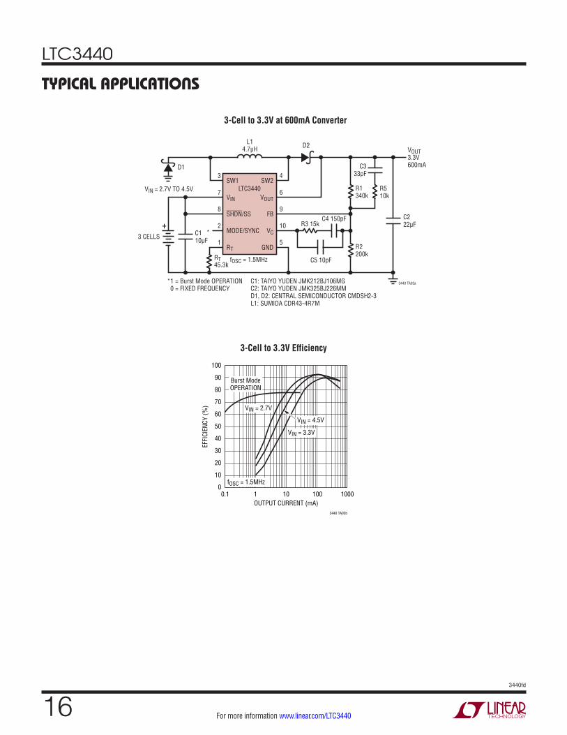
3-Cell to 3.3V at 600mA Converter
3-Cell to 3.3V Efficiency
typical applications
SW1
VIN
SHDN/SS
MODE/SYNC
RT
SW2
VOUT
FB
VC
GND
3
7
8
2
1
4
6
9
10
5
LTC3440
L14.7µH
D1
R3 15k
R510k
R1340k
R2200k
3440 TA03a
RT45.3k
fOSC = 1.5MHz
C1: TAIYO YUDEN JMK212BJ106MGC2: TAIYO YUDEN JMK325BJ226MMD1, D2: CENTRAL SEMICONDUCTOR CMDSH2-3L1: SUMIDA CDR43-4R7M
*1 = Burst Mode OPERATION 0 = FIXED FREQUENCY
C110µF3 CELLS
VIN = 2.7V TO 4.5V
*
C4 150pF
C333pF
D2
C5 10pF
C222µF
VOUT3.3V600mA
+
OUTPUT CURRENT (mA)
30
EFFI
CIEN
CY (%
)
90
100
20
10
80
50
70
60
40
0.1 10 100 1000
3440 TA03b
01
Burst ModeOPERATION
VIN = 2.7V
VIN = 3.3V
fOSC = 1.5MHz
VIN = 4.5V
LTC3440
173440fd
For more information www.linear.com/LTC3440
typical applications
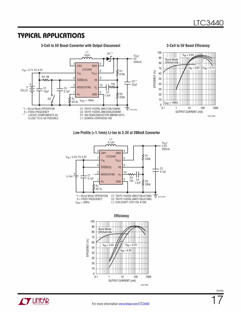
Low Profile (<1.1mm) Li-Ion to 3.3V at 200mA Converter
SW1
VIN
SHDN/SS
MODE/SYNC
RT
SW2
VOUT
FB
VC
GND
3
7
8
2
1
4
6
9
10
5
LTC3440
L14.7µH
R1340k
R2200k
R315k
3440 TA04a
RT30.1k
C1: TAIYO YUDEN JMK212BJ475MGC2: TAIYO YUDEN JMK212BJ475MGL1: COILCRAFT LPO1704-472M
*1 = Burst Mode OPERATION 0 = FIXED FREQUENCYfOSC = 2MHz
C14.7µF
Li-Ion
VIN = 2.5V TO 4.2V
*+C4
1.5nF
C24.7µF
VOUT3.3V200mA
OUTPUT CURRENT (mA)
30
EFFI
CIEN
CY (%
)
90
100
20
10
80
50
70
60
40
0.1 10 100 1000
3440 TA04b
01
Burst ModeOPERATION
VIN = 2.5V
VIN = 3.3V
VIN = 4.2V
Efficiency
3-Cell to 5V Boost Converter with Output Disconnect
SW1
VIN
SHDN/SS
MODE/SYNC
RT
SW2
VOUT
FB
VC
GND
3
7
8
2
1
4
6
9
10
5
LTC3440
L110µH
R1619k
R2200k
3440 TA06a
RT60.4k
C1: TAIYO YUDEN JMK212BJ106MGC2: TAIYO YUDEN JMK325BJ226MMD1: ON SEMICONDUCTOR MBRM120T3L1: SUMIDA CDRH4D28-100
*1 = Burst Mode OPERATION 0 = FIXED FREQUENCY** LOCATE COMPONENTS AS CLOSE TO IC AS POSSIBLE
C110µF
C30.1µF
3CELLS
R4 1M
VIN = 2.7V TO 4.5V
*
SD
C41.5nF
15k
fOSC = 1MHz
C2**22µF
VOUT5V300mA
+
D1**
OUTPUT CURRENT (mA)
30
EFFI
CIEN
CY (%
)
90
100
20
10
80
50
70
60
40
0.1 10 100 1000
3440 TA06b
01
Burst ModeOPERATION
VIN = 2.7V
fOSC = 1MHz
VIN = 3.6V
VIN = 4.5V
3-Cell to 5V Boost Efficiency
LTC3440
183440fd
For more information www.linear.com/LTC3440
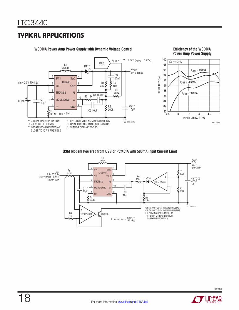
typical applications
SW1
VIN
SHDN/SS
MODE/SYNC
RT
SW2
VOUT
FB
VC
GND
3
7
8
2
1
4
6
9
10
5
LTC3440
L13.3µH
R1340k
R510k
R2200k
R3 15k
D1**
3440 TA07a
RT30.1k
C1, C2: TAIYO YUDEN JMK212BJ106MMD1: ON SEMICONDUCTOR MBRM120T3L1: SUMIDA CDRH4D28-3R3
*1 = Burst Mode OPERATION 0 = FIXED FREQUENCY** LOCATE COMPONENTS AS CLOSE TO IC AS POSSIBLE
C110µF
fOSC = 2MHz
Li-Ion
VIN = 2.5V TO 4.2V
*+
C4 150pF
C5 10pFC2**10µF
VOUT0.4V TO 5V
C333pF
VOUT = 3.3V – 1.7V • (VDAC – 1.22V)
R6200k
DAC
WCDMA Power Amp Power Supply with Dynamic Voltage Control Efficiency of the WCDMA Power Amp Power Supply
INPUT VOLTAGE (V)2.5
EFFI
CIEN
CY (%
)
92
96
100
4.5
3440 TA07b
88
84
90
94
98
86
82
803 3.5 4 5
VOUT = 3.4V
IOUT = 100mA
IOUT = 250mA
IOUT = 600mA
SW1
VIN
SHDN/SS
MODE/SYNC
RT
SW2
VOUT
FB
VC
GND
3
7
8
2
1
4
6
9
10
5
LTC3440
L110µH
R524k
3440 TA08
RT60.4k
RS0.1Ω
R41k
C1: TAIYO YUDEN JMK212BJ106MGC2: TAIYO YUDEN JMK325BJ226MML1: SUMIDA CDRH-4D28-100*1 = Burst Mode OPERATION 0 = FIXED FREQUENCY
C110µF
VIN2.5V TO 5.5V
USB/PCMCIA POWER500mA MAX
*
VOUT3.6V2A(PULSED)
C510nF
R6130k
R1392k
R2200k
–
+
1/2 LT1490A 2N3906
–
+1/2 LT1490A
1N914 C6 TO C9470µF×4
1.22 • R4R5 • RS
ICURRENTLIMIT =
GSM Modem Powered from USB or PCMCIA with 500mA Input Current Limit
LTC3440
193440fd
For more information www.linear.com/LTC3440
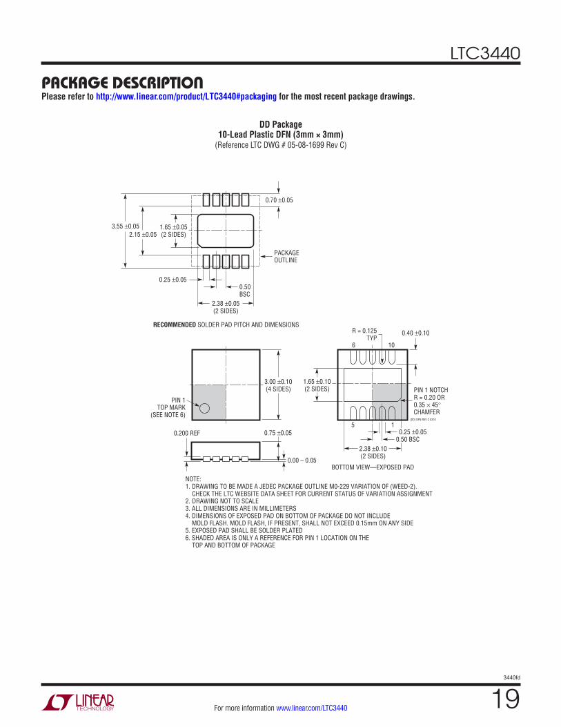
package DescriptionPlease refer to http://www.linear.com/product/LTC3440#packaging for the most recent package drawings.
DD Package10-Lead Plastic DFN (3mm × 3mm)
(Reference LTC DWG # 05-08-1699 Rev C)
3.00 ±0.10(4 SIDES)
NOTE:1. DRAWING TO BE MADE A JEDEC PACKAGE OUTLINE M0-229 VARIATION OF (WEED-2). CHECK THE LTC WEBSITE DATA SHEET FOR CURRENT STATUS OF VARIATION ASSIGNMENT2. DRAWING NOT TO SCALE3. ALL DIMENSIONS ARE IN MILLIMETERS4. DIMENSIONS OF EXPOSED PAD ON BOTTOM OF PACKAGE DO NOT INCLUDE MOLD FLASH. MOLD FLASH, IF PRESENT, SHALL NOT EXCEED 0.15mm ON ANY SIDE5. EXPOSED PAD SHALL BE SOLDER PLATED6. SHADED AREA IS ONLY A REFERENCE FOR PIN 1 LOCATION ON THE TOP AND BOTTOM OF PACKAGE
0.40 ±0.10
BOTTOM VIEW—EXPOSED PAD
1.65 ±0.10(2 SIDES)
0.75 ±0.05
R = 0.125TYP
2.38 ±0.10(2 SIDES)
15
106
PIN 1TOP MARK
(SEE NOTE 6)
0.200 REF
0.00 – 0.05
(DD) DFN REV C 0310
0.25 ±0.05
2.38 ±0.05(2 SIDES)
RECOMMENDED SOLDER PAD PITCH AND DIMENSIONS
1.65 ±0.05(2 SIDES)2.15 ±0.05
0.50BSC
0.70 ±0.05
3.55 ±0.05
PACKAGEOUTLINE
0.25 ±0.050.50 BSC
DD Package10-Lead Plastic DFN (3mm × 3mm)
(Reference LTC DWG # 05-08-1699 Rev C)
PIN 1 NOTCHR = 0.20 OR0.35 × 45°CHAMFER
LTC3440
203440fd
For more information www.linear.com/LTC3440
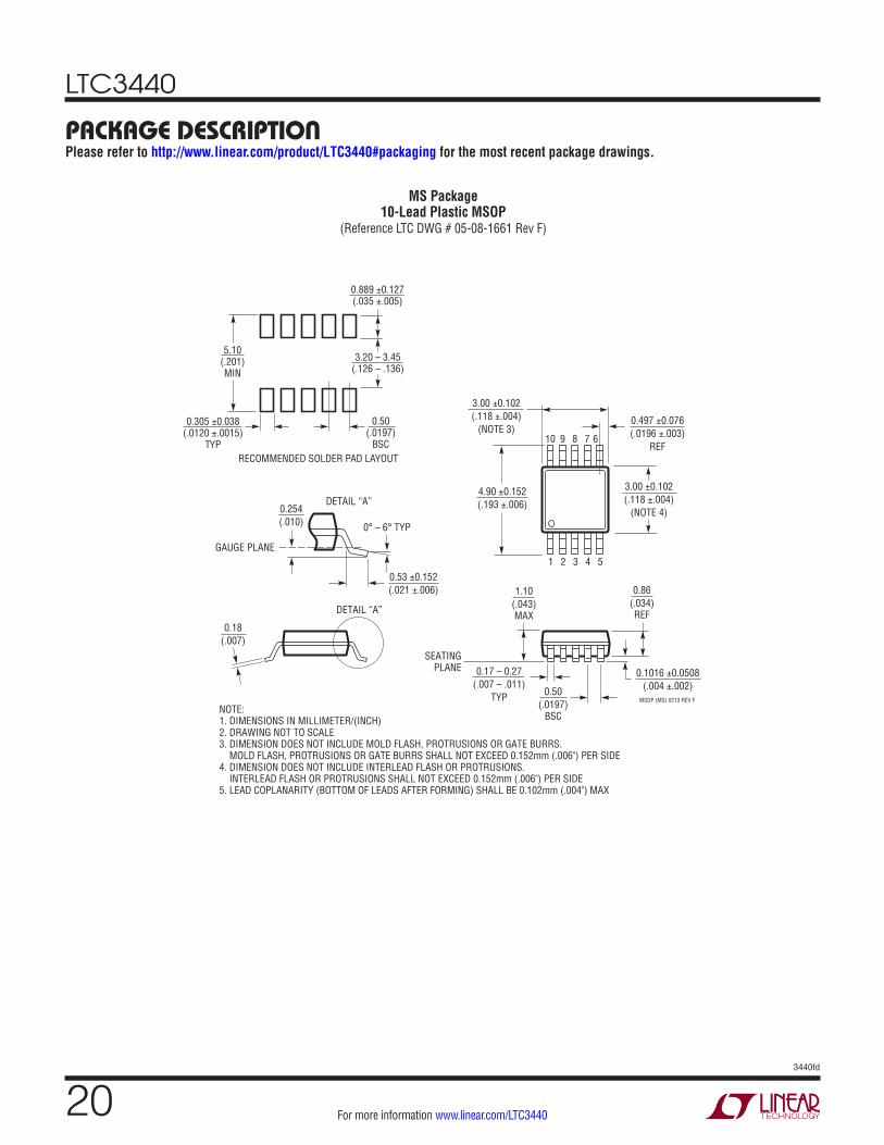
package DescriptionPlease refer to http://www.linear.com/product/LTC3440#packaging for the most recent package drawings.
MSOP (MS) 0213 REV F
0.53 ±0.152(.021 ±.006)
SEATINGPLANE
0.18(.007)
1.10(.043)MAX
0.17 – 0.27(.007 – .011)
TYP
0.86(.034)REF
0.50(.0197)
BSC
1 2 3 4 5
4.90 ±0.152(.193 ±.006)
0.497 ±0.076(.0196 ±.003)
REF8910 7 6
3.00 ±0.102(.118 ±.004)
(NOTE 3)
3.00 ±0.102(.118 ±.004)
(NOTE 4)
NOTE:1. DIMENSIONS IN MILLIMETER/(INCH)2. DRAWING NOT TO SCALE3. DIMENSION DOES NOT INCLUDE MOLD FLASH, PROTRUSIONS OR GATE BURRS. MOLD FLASH, PROTRUSIONS OR GATE BURRS SHALL NOT EXCEED 0.152mm (.006") PER SIDE4. DIMENSION DOES NOT INCLUDE INTERLEAD FLASH OR PROTRUSIONS. INTERLEAD FLASH OR PROTRUSIONS SHALL NOT EXCEED 0.152mm (.006") PER SIDE5. LEAD COPLANARITY (BOTTOM OF LEADS AFTER FORMING) SHALL BE 0.102mm (.004") MAX
0.254(.010) 0° – 6° TYP
DETAIL “A”
DETAIL “A”
GAUGE PLANE
5.10(.201)MIN
3.20 – 3.45(.126 – .136)
0.889 ±0.127(.035 ±.005)
RECOMMENDED SOLDER PAD LAYOUT
0.305 ±0.038(.0120 ±.0015)
TYP
0.50(.0197)
BSC
0.1016 ±0.0508(.004 ±.002)
MS Package10-Lead Plastic MSOP
(Reference LTC DWG # 05-08-1661 Rev F)
MS Package10-Lead Plastic MSOP
(Reference LTC DWG # 05-08-1661 Rev F)
LTC3440
213440fd
For more information www.linear.com/LTC3440
Information furnished by Linear Technology Corporation is believed to be accurate and reliable. However, no responsibility is assumed for its use. Linear Technology Corporation makes no representa-tion that the interconnection of its circuits as described herein will not infringe on existing patent rights.
revision historyREV DATE DESCRIPTION PAGE NUMBER
C 8/14 Modified filter pole equation in Closing the Feedback Loop section 13
D 10/16 Added equation to calculate VOUT
Modified Operating Frequency Selection section6
13
(Revision history begins at Rev C)
LTC3440
223440fd
For more information www.linear.com/LTC3440
Linear Technology Corporation1630 McCarthy Blvd., Milpitas, CA 95035-7417
LINEAR TECHNOLOGY CORPORATION 2001
LT 1016 REV D • PRINTED IN USA
(408) 432-1900 ● FAX: (408) 434-0507 ● www.linear.com/LTC3440
relateD parts
typical application
PART NUMBER DESCRIPTION COMMENTS
LT1613 550mA(ISW), 1.4MHz, High Efficiency Step-Up DC/DC Converter
90% Efficiency, VIN: 0.9V to 10V, VOUT(MIN) = 34V, IQ = 3mA, ISD = <1µA, ThinSOT™ Package
LT1618 1.5A(ISW), 1.25MHz, High Efficiency Step-Up DC/DC Converter
90% Efficiency, VIN: 1.6V to 18V, VOUT(MIN) = 35V, IQ = 1.8mA, ISD = <1µA, MS10 Package
LTC1877 600mA(IOUT), 550kHz, Synchronous Step-Down DC/DC Converter
95% Efficiency, VIN: 2.7V to 10V, VOUT(MIN) = 0.8V, IQ = 10µA, ISD = <1µA, MS8 Package
LTC1878 600mA(IOUT), 550kHz, Synchronous Step-Down DC/DC Converter
95% Efficiency, VIN: 2.7V to 6V, VOUT(MIN) = 0.8V, IQ = 10µA, ISD = <1µA, MS8 Package
LTC1879 1.2A(IOUT), 550kHz, Synchronous Step-Down DC/DC Converter
95% Efficiency, VIN: 2.7V to 10V, VOUT(MIN) = 0.8V, IQ = 15µA, ISD = <1µA, TSSOP16 Package
LT1961 1.5A(ISW), 1.25MHz, High Efficiency Step-Up DC/DC Converter
90% Efficiency, VIN: 3V to 25V, VOUT(MIN) = 35V, IQ = 0.9mA, ISD = 6µA, MS8E Package
LTC3400/LTC3400B 600mA(ISW), 1.2MHz, Synchronous Step-Up DC/DC Converter
92% Efficiency, VIN: 0.85V to 5V, VOUT(MIN) = 5V, IQ = 19µA/300µA, ISD = <1µA, ThinSOT Package
LTC3401 1A(ISW), 3MHz, Synchronous Step-Up DC/DC Converter 97% Efficiency, VIN: 0.5V to 5V, VOUT(MIN) = 6V, IQ = 38µA, ISD = <1µA, MS10 Package
LTC3402 2A(ISW), 3MHz, Synchronous Step-Up DC/DC Converter 97% Efficiency, VIN: 0.5V to 5V, VOUT(MIN) = 6V, IQ = 38µA, ISD = <1µA, MS10 Package
LTC3405/LTC3405A 300mA(IOUT), 1.5MHz, Synchronous Step-Down DC/DC Converter
95% Efficiency, VIN: 2.7V to 6V, VOUT(MIN) = 0.8V, IQ = 20µA, ISD = <1µA, ThinSOT Package
LTC3406/LTC3406B 600mA(IOUT), 1.5MHz, Synchronous Step-Down DC/DC Converter
95% Efficiency, VIN: 2.5V to 5.5V, VOUT(MIN) = 0.6V, IQ = 20µA, ISD = <1µA, ThinSOT Package
LTC3411 1.25A(IOUT), 4MHz, Synchronous Step-Down DC/DC Converter
95% Efficiency, VIN: 2.5V to 5.5V, VOUT(MIN) = 0.8V, IQ = 60µA, ISD = <1µA, MS10 Package
LTC3412 2.5A(IOUT), 4MHz, Synchronous Step-Down DC/DC Converter
95% Efficiency, VIN: 2.5V to 5.5V, VOUT(MIN) = 0.8V, IQ = 60µA, ISD = <1µA, TSSOP16E Package
LTC3441/LTC3443 1.2A(IOUT), 1MHz/0.6MHz, Micropower Synchronous Buck-Boost DC/DC Converter
95% Efficiency, VIN: 2.4V to 5.5V, VOUT(MIN): 2.4V to 5.25V, IQ = 25µA, ISD = <1µA, DFN Package
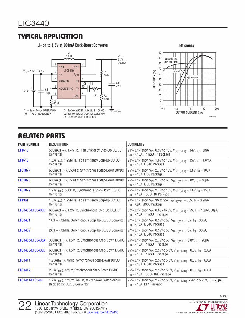
Efficiency
3440 TA05
OUTPUT CURRENT (mA)
EFFI
CIEN
CY (%
)
100
90
80
70
60
50
40
30
20
10
00.1 10 100 10001.0
VIN = 4.2V
VIN = 3.3V
Burst ModeOPERATION
Li-Ion to 3.3V at 600mA Buck-Boost Converter
SW1
VIN
SHDN/SS
MODE/SYNC
RT
SW2
VOUT
FB
VC
GND
3
7
8
2
1
4
6
9
10
5
LTC3440
L110µH
R1340k
R2200k
R315k
3440 TA01
RT60.4k
C1: TAIYO YUDEN JMK212BJ106MGC2: TAIYO YUDEN JMK325BJ226MML1: SUMIDA CDRH6D38-100
*1 = Burst Mode OPERATION 0 = FIXED FREQUENCY
C110µF
Li-Ion
VIN = 2.7V TO 4.2V
*+C5 1.5nF C2
22µF
VOUT3.3V600mA