Embed Size (px)
Citation preview

LMC7101/LMC7101QJune 12, 2009
Tiny Low Power Operational Amplifier with Rail-to-RailInput and OutputGeneral DescriptionThe LMC7101 is a high performance CMOS operational am-plifier available in the space saving 5-Pin SOT23 Tiny pack-age. This makes the LMC7101 ideal for space and weightcritical designs. The performance is similar to a single ampli-fier of the LMC6482/LMC6484 type, with rail-to-rail input andoutput, high open loop gain, low distortion, and low supplycurrents.
The main benefits of the Tiny package are most apparent insmall portable electronic devices, such as mobile phones,pagers, notebook computers, personal digital assistants, andPCMCIA cards. The tiny amplifiers can be placed on a boardwhere they are needed, simplifying board layout.
Features■ Tiny 5-Pin SOT23 package saves space—typical circuit
layouts take half the space of 8-Pin SOIC designs
■ Guaranteed specs at 2.7V, 3V, 5V, 15V supplies
■ Typical supply current 0.5 mA at 5V
■ Typical total harmonic distortion of 0.01% at 5V
■ 1.0 MHz gain-bandwidth
■ Similar to popular LMC6482/LMC6484
■ Rail-to-rail input and output
■ Temperature Range –40°C to 125°C (LMC7101Q)
Applications■ Mobile communications
■ Notebooks and PDAs
■ Battery powered products
■ Sensor interface
■ Automotive applications (LMC7101Q)
Connection Diagram
5-Pin SOT23
1199102
Top View
Ordering Information
Package Part Number Package
Marking
Transport Media NSC Drawing Features
5-Pin SOT23
LMC7101AIM5A00A
1k Units on Tape and Reel
MF05A
LMC7101AIM5X 3k Units Tape and Reel
LMC7101BIM5A00B
1k Units on Tape and Reel
LMC7101BIM5X 3k Units Tape and Reel
LMC7101QM5AT6A
1k Units on Tape and Reel –40°C to 125°C
Operating rangeLMC7101QM5X 3k Units Tape and Reel
* The LMC7101Q incorporates enhanced manufacturing and support processes for the automotive market, including defect detection methodologies.
© 2009 National Semiconductor Corporation 11991 www.national.com
LM
C7101/L
MC
7101Q
Tin
y L
ow
Po
wer O
pera
tion
al A
mp
lifier w
ith R
ail-to
-Rail In
pu
t an
d O
utp
ut

Absolute Maximum Ratings (Note 1)
If Military/Aerospace specified devices are required,please contact the National Semiconductor Sales Office/Distributors for availability and specifications.
ESD Tolerance (Note 2)
Human Body Model 1000V
Machine Model 200V
Charged Device Model 1000V
Difference Input Voltage ±Supply Voltage
Voltage at Input/Output Pin (V+) + 0.3V, (V−) − 0.3V
Supply Voltage (V+ − V−) 16V
Current at Input Pin ±5 mA
Current at Output Pin (Note 3) ±35 mA
Current at Power Supply Pin 35 mA
Lead Temp. (Soldering, 10 sec.) 260°C
Storage Temperature Range −65°C to +150°C
Junction Temperature (Note 4) 150°C
Recommended Operating
Conditions (Note 1)
Supply Voltage 2.7V ≤ V+ ≤ 15.5V
Temperature Range
LMC7101AI, LMC7101BI −40°C to 85°C
LMC7101Q −40°C to 125°C
Thermal Resistance (θJA)
5-Pin SOT23 325°C/W
2.7V Electrical CharacteristicsUnless otherwise specified, all limits guaranteed for TJ = 25°C, V+ = 2.7V, V− = 0V, VCM = VO = V+/2 and RL > 1 MΩ. Boldfacelimits apply at the temperature extremes.
Symbol Parameter ConditionsTyp
(Note 5)
LMC7101AI
Limit
(Note 6)
LMC7101BI
Limit
(Note 6)
LMC7101Q
Limit
(Notes 6, 10)
Units
VOS Input Offset Voltage Average Drift V+ = 2.7V 0.11 6 9 9 mV max
TCVOS Input Offset Voltage 1 μV/°C
IB Input Bias Current 1.0 64 64 1000 pA max
IOS Input Offset Current 0.5 32 32 2000 pA max
RIN Input Resistance >1 Tera Ω
CMRR Common-Mode Rejection Ratio0V ≤ VCM ≤ 2.7V
V+ = 2.7V70 55 50 50 dB min
VCM
Input Common Mode Voltage
RangeFor CMRR ≥ 50 dB
0.0 0.0 0.0 0.0 V min
3.0 2.7 2.7 2.7 V max
PSRR Power Supply Rejection Ratio
V+ = 1.35V to 1.65V
V− = −1.35V to −1.65V
VCM = 0
60 50 45 45 dB min
CIN Common-Mode Input Capacitance 3 pF
VO Output Swing
RL = 2 kΩ2.45 2.15 2.15 2.15 V min
0.25 0.5 0.5 0.5 V max
RL = 10 kΩ2.68 2.64 2.64 2.64 V min
0.025 0.06 0.06 0.06 V max
IS Supply Current 0.5 0.81
0.95
0.81
0.95
0.81
0.95
mA max
SR Slew Rate (Note 8) 0.7 V/μs
GBW Gain-Bandwidth Product 0.6 MHz
www.national.com 2
LM
C7101/L
MC
7101Q

3V DC Electrical CharacteristicsUnless otherwise specified, all limits guaranteed for TJ = 25°C, V+ = 3V, V− = 0V, VCM = 1.5V, VO = V+/2 and RL = 1 MΩ. Bold-face limits apply at the temperature extremes.
Symbol Parameter ConditionsTyp
(Note 5)
LMC7101AI
Limit
(Note 6)
LMC7101BI
Limit
(Note 6)
LMC7101Q
Limit
(Notes 6, 10)
Units
VOS Input Offset Voltage 0.114
6
7
97 mV max
TCVOS Input Offset Voltage Average Drift 1 μV/°C
IB Input Current 1.0 64 64 1000 pA max
IOS Input Offset Current 0.5 32 32 2000 pA max
RIN Input Resistance >1 Tera Ω
CMRR Common-Mode Rejection Ratio0V ≤ VCM ≤ 3V
V+ = 3V74 64 60 60 db min
VCM
Input Common-Mode Voltage
RangeFor CMRR ≥ 50 dB
0.0 0.0 0.0 0.0 V min
3.3 3.0 3.0 3.0 V max
PSRR Power Supply Rejection Ratio
V+ = 1.5V to 7.5V
V− = −1.5V to −7.5V
VO = VCM = 0
80 68 60 60 dBmin
CIN Common-Mode Input Capacitance 3 pF
VO Output Swing
RL = 2 kΩ2.8 2.6 2.6 2.6 V min
0.2 0.4 0.4 0.4 V max
RL = 600Ω2.7 2.5 2.5 2.5 V min
0.37 0.6 0.6 0.6 V max
IS Supply Current
0.50.81
0.95
0.81
0.95
0.81
0.95mA max
3 www.national.com
LM
C7101/L
MC
7101Q

5V DC Electrical CharacteristicsUnless otherwise specified, all limits guaranteed for TJ = 25°C, V+ = 5V, V− = 0V, VCM = 1.5V, VO = V+/2 and RL = 1 MΩ. Boldfacelimits apply at the temperature extremes.
Symbol Parameter ConditionsTyp
(Note 5)
LMC7101AI
Limit
(Note 6)
LMC7101BI
Limit
(Note 6)
LMC7101Q
Limit
(Notes 6, 10)
Units
VOS Input Offset Voltage V+ = 5V0.11 3
5
7
9
7
9
mV max
TCVOS Input Offset Voltage Average Drift 1.0 μV/°C
IB Input Current 1 64 64 1000 pA max
IOS Input Offset Current 0.5 32 32 2000 pA max
RIN Input Resistance >1 Tera Ω
CMRR Common-Mode Rejection Ratio
0V ≤ VCM ≤ 5V
LMC7101Q @ 125°C
0.2V ≤ VCM ≤ 4.8V
82 65
60
60
55
60
55
db min
+PSRRPositive Power Supply Rejection
Ratio
V+ = 5V to 15V
V− = 0V, VO = 1.5V
82 70
65
65
62
65
62
dB min
−PSRRNegative Power Supply Rejection
Ratio
V− = −5V to −15V
V+ = 0V, VO = −1.5V
82 70
65
65
62
65
62
dB min
VCM
Input Common-Mode Voltage
Range
For CMRR ≥ 50 dB−0.3 −0.20
0.00
−0.20
0.00
−0.2
0.2
V min
5.3 5.20
5.00
5.20
5.00
5.2
4.8
V max
CIN Common-Mode Input Capacitance 3 pF
VO Output Swing
RL = 2 kΩ4.9 4.7
4.6
4.7
4.6
4.7
4.54
V min
0.1 0.18
0.24
0.18
0.24
0.18
0.28
V max
RL = 600Ω4.7 4.5
4.24
4.5
4.24
4.5
4.28
V min
0.3 0.5
0.65
0.5
0.65
0.5
0.8
V max
ISC Output Short Circuit Current
VO = 0V 24 Sourcing 2416
11
16
11
16
9
mA min
VO = 5V Sinking 1911
7.5
11
7.5
11
5.8
mA min
IS Supply Current 0.50.85
1.0
0.85
1.0
0.85
1.0
mA max
5V AC Electrical CharacteristicsUnless otherwise specified, all limits guaranteed for TJ = 25°C, V+ = 5V, V− = 0V, VCM = 1.5V, VO = V+/2 and RL = 1 MΩ. Boldfacelimits apply at the temperature extremes.
Symbol Parameter ConditionsTyp
(Note 5)
LMC7101AI
Limit
(Note 6)
LMC7101BI
Limit
(Note 6)
Units
THD Total Harmonic Distortionf = 10 kHz, AV = −2
RL = 10 kΩ, VO = 4.0 VPP
0.01 %
SR Slew Rate 1.0 V/μs
GBW Gain Bandwidth Product 1.0 MHz
www.national.com 4
LM
C7101/L
MC
7101Q

15V DC Electrical CharacteristicsUnless otherwise specified, all limits guaranteed for TJ = 25°C, V+ = 15V, V− = 0V, VCM = 1.5V, VO = V+/2 and RL = 1 MΩ.Boldface limits apply at the temperature extremes.
Symbol Parameter ConditionsTyp
(Note 5)
LMC7101AI
Limit
(Note 6)
LMC7101BI
Limit
(Note 6)
LMC7101Q
Limit
(Notes 6, 10)
Units
VOS Input Offset Voltage 0.11 mV max
TCVOS Input Offset Voltage Average Drift 1.0 μV/°C
IB Input Current 1.0 64 64 1000 pA max
IOS Input Offset Current 0.5 32 32 2000 pA max
RIN Input Resistance >1 Tera Ω
CMRR Common-Mode Rejection Ratio
0V ≤ VCM ≤ 15V
LMC7101Q @°125C
0.2V ≤ VCM ≤ 14.8V
82 70
65
65
60
65
60
dB min
+PSRRPositive Power Supply Rejection
Ratio
V+ = 5V to 15V
V− = 0V, VO = 1.5V
82 70
65
65
62
65
62
dB min
−PSRRNegative Power Supply Rejection
Ratio
V− = −5V to −15V
V+ = 0V, VO = −1.5V
82 70
65
65
62
65
62
dB min
VCM
Input Common-Mode Voltage
Range
V+ = 5V
For CMRR ≥ 50 dB
−0.3 −0.20
0.00
−0.20
0.00
−0.2
0.2
V min
15.3 15.20
15.00
15.20
15.00
15.2
14.8
V max
AV
Large Signal Voltage Gain
(Note 7)
RL = 2 kΩSourcing
340 80
40
80
40
80
30V/mV
Sinking24 15
10
15
10
15
4
RL = 600ΩSourcing 300 34 34 34
V/mVSinking 15 6 6 6
CIN Input Capacitance 3 pF
VO Output Swing
V+ = 15V
RL = 2 kΩ14.7 14.4
14.2
14.4
14.2
14.4
14.2
V min
0.16 0.32
0.45
0.32
0.45
0.32
0.45
V max
V+ = 15V
RL = 600Ω14.1 13.4
13.0
13.4
13.0
13.4
12.85
V min
0.5 1.0
1.3
1.0
1.3
1.0
1.5
V max
ISC
Output Short Circuit Current
(Note 9)
VO = 0V Sourcing50 30
20
30
20
30
20mA min
VO = 12V Sinking50 30
20
30
20
30
20
IS Supply Current 0.8 1.50
1.71
1.50
1.71
1.50
1.75
mA max
5 www.national.com
LM
C7101/L
MC
7101Q

15V AC Electrical CharacteristicsUnless otherwise specified, all limits guaranteed for TJ = 25°C, V+ = 15V, V− = 0V, VCM = 1.5V, VO = V+/2 and RL = 1 MΩ.Boldface limits apply at the temperature extremes.
Symbol Parameter ConditionsTyp
(Note 5)
LMC7101AI
Limit
(Note 6)
LMC7101BI
Limit
(Note 6)
LMC7101Q
Limit
(Notes 6, 10)
Units
SRSlew Rate
(Note 8)V+ = 15V 1.1
0.5
0.4
0.5
0.4
0.5
0.4V/μs
min
GBW Gain-Bandwidth Product V+ = 15V 1.1 MHz
φm Phase Margin 45 deg
Gm Gain Margin 10 dB
en Input-Referred Voltage Noise f = 1 kHz, VCM = 1V 37
in Input-Referred Current Noise f = 1 kHz 1.5
THD Total Harmonic Distortionf = 10 kHz, AV = −2
RL = 10 kΩ, VO = 8.5 VPP
0.01
%
Note 1: Absolute Maximum Ratings indicate limits beyond which damage to the device may occur. Operating Ratings indicate conditions for which the device isintended to be functional, but specific performance is not guaranteed. For guaranteed specifications and the test conditions, see the Electrical Characteristics.
Note 2: Human Body Model is 1.5 kΩ in series with 100 pF.
Note 3: Applies to both single-supply and split-supply operation. Continuous short operation at elevated ambient temperature can result in exceeding the maximumallowed junction temperature at 150°C.
Note 4: The maximum power dissipation is a function of TJ(MAX), θJA and TA. The maximum allowable power dissipation at any ambient temperature isPD = (TJ(MAX) − TA)/θJA. All numbers apply for packages soldered directly into a PC board.
Note 5: Typical Values represent the most likely parametric norm.
Note 6: All limits are guaranteed by testing or statistical analysis.
Note 7: V+ = 15V, VCM = 1.5V and RL connect to 7.5V. For sourcing tests, 7.5V ≤ VO ≤ 12.5V. For sinking tests, 2.5V ≤ VO ≤ 7.5V.
Note 8: V+ = 15V. Connected as a voltage follower with a 10V step input. Number specified is the slower of the positive and negative slew rates. RL = 100 kΩconnected to 7.5V. Amp excited with 1 kHz to produce VO = 10 VPP.
Note 9: Do not short circuit output to V+ when V+ is greater than 12V or reliability will be adversely affected.
Note 10: When operated at temperature between −40°C and 85°C, the LMC7101Q will meet LMC7101BI specifications.
www.national.com 6
LM
C7101/L
MC
7101Q

2.7V Typical Performance Characteristics V+ = 2.7V, V− = 0V, TA = 25°C, unless otherwise specified.
Open Loop Frequency Response
1199116
Input Voltage vs. Output Voltage
1199117
Gain and Phase vs. Capacitance Load
1199118
Gain and Phase vs. Capacitance Load
1199119
dVOS vs. Supply Voltage
1199120
dVOS vs. Common Mode Voltage
1199121
7 www.national.com
LM
C7101/L
MC
7101Q

Sinking Current vs. Output Voltage
1199122
Sourcing Current vs. Output Voltage
1199123
www.national.com 8
LM
C7101/L
MC
7101Q

3V Typical Performance Characteristics V+ = 3V, V− = 0V, TA = 25°C, unless otherwise specified.
Open Loop Frequency Response
1199124
Input Voltage vs. Output Voltage
1199125
Input Voltage Noise vs. Input Voltage
1199126
Sourcing Current vs. Output Voltage
1199127
Sinking Current vs. Output Voltage
1199128
CMRR vs. Input Voltage
1199129
9 www.national.com
LM
C7101/L
MC
7101Q

5V Typical Performance Characteristics V+ = 5V, V− = 0V, TA = 25°C, unless otherwise specified.
Open Loop Frequency Response
1199130
Input Voltage vs. Output Voltage
1199131
Input Voltage Noise vs. Input Voltage
1199132
Sourcing Current vs, Output Voltage
1199133
Sinking Current vs. Output Voltage
1199134
CMRR vs. Input Voltage
1199135
www.national.com 10
LM
C7101/L
MC
7101Q

15V Typical Performance Characteristics V+ = +15V, V− = 0V, TA = 25°C, unless otherwise specified.
Open Loop Frequency Response
1199136
Input Voltage vs. Output Voltage
1199137
Input Voltage Noise vs. Input Voltage
1199138
Sourcing Current vs. Output Voltage
1199139
Sinking Current vs. Output Voltage
1199140
CMRR vs. Input Voltage
1199141
11 www.national.com
LM
C7101/L
MC
7101Q

Supply Current vs. Supply Voltage
1199142
Input Current vs. Temperature
1199143
Output Voltage Swing vs. Supply Voltage
1199144
Input Voltage Noise vs. Frequency
1199145
Positive PSRR vs. Frequency
1199146
Negative PSRR vs. Frequency
1199147
www.national.com 12
LM
C7101/L
MC
7101Q

CMRR vs. Frequency
1199148
Open Loop Frequency Response @ −40°C
1199149
Open Loop Frequency Response @ 25°C
1199150
Open Loop Frequency Response @ 85°C
1199151
Maximum Output Swing vs. Frequency
1199152
Gain and Phase vs. Capacitive Load
1199153
13 www.national.com
LM
C7101/L
MC
7101Q

Gain and Phase vs. Capacitive Load
1199154
Output Impedance vs. Frequency
1199155
Slew Rate vs. Temperature
1199156
Slew Rate vs. Supply Voltage
1199157
Inverting Small Signal Pulse Response
1199158
Inverting Small Signal Pulse Response
1199159
www.national.com 14
LM
C7101/L
MC
7101Q

Inverting Small Signal Pulse Response
1199160
Inverting Large Signal Pulse Response
1199161
Inverting Large Signal Pulse Response
1199162
Inverting Large Signal Pulse Response
1199163
Non-Inverting Small Signal Pulse Response
1199164
Non-Inverting Small Signal Pulse Response
1199165
15 www.national.com
LM
C7101/L
MC
7101Q

Non-Inverting Small Signal Pulse Response
1199166
Non-Inverting Large Signal Pulse Response
1199167
Non-Inverting Large Signal Pulse Response
1199168
Non-Inverting Large Signal Pulse Response
1199169
Stability vs. Capacitive Load
1199170
Stability vs. Capacitive Load
1199171
www.national.com 16
LM
C7101/L
MC
7101Q

Stability vs. Capacitive Load
1199175
Stability vs. Capacitive Load
1199176
Stability vs. Capacitive Load
1199177
Stability vs. Capacitive Load
1199178
17 www.national.com
LM
C7101/L
MC
7101Q

Application Information
1.0 BENEFITS OF THE LMC7101TINY AMP
Size
The small footprint of the SOT 23-5 packaged Tiny amp,(0.120 x 0.118 inches, 3.05 x 3.00 mm) saves space on print-ed circuit boards, and enable the design of smaller electronicproducts. Because they are easier to carry, many customersprefer smaller and lighter products.
Height
The height (0.056 inches, 1.43 mm) of the Tiny amp makes itpossible to use it in PCMCIA type III cards.
Signal Integrity
Signals can pick up noise between the signal source and theamplifier. By using a physically smaller amplifier package, theTiny amp can be placed closer to the signal source, reducingnoise pickup and increasing signal integrity. The Tiny ampcan also be placed next to the signal destination, such as abuffer for the reference of an analog to digital converter.
Simplified Board Layout
The Tiny amp can simplify board layout in several ways. First,by placing an amp where amps are needed, instead of routingsignals to a dual or quad device, long pc traces may be avoid-ed.
By using multiple Tiny amps instead of duals or quads, com-plex signal routing and possibly crosstalk can be reduced.
Low THD
The high open loop gain of the LMC7101 amp allows it toachieve very low audio distortion—typically 0.01% at 10 kHzwith a 10 kΩ load at 5V supplies. This makes the Tiny anexcellent for audio, modems, and low frequency signal pro-cessing.
Low Supply Current
The typical 0.5 mA supply current of the LMC7101 extendsbattery life in portable applications, and may allow the reduc-tion of the size of batteries in some applications.
Wide Voltage Range
The LMC7101 is characterized at 15V, 5V and 3V. Perfor-mance data is provided at these popular voltages. This widevoltage range makes the LMC7101 a good choice for deviceswhere the voltage may vary over the life of the batteries.
2.0 INPUT COMMON MODE
Voltage Range
The LMC7101 does not exhibit phase inversion when an inputvoltage exceeds the negative supply voltage. Figure 1 showsan input voltage exceeding both supplies with no resultingphase inversion of the output.
The absolute maximum input voltage is 300 mV beyond eitherrail at room temperature. Voltages greatly exceeding thismaximum rating, as in Figure 2, can cause excessive currentto flow in or out of the input pins, adversely affecting reliability.
1199108
FIGURE 1. An Input Voltage Signal Exceeds theLMC7101 Power Supply Voltages with
No Output Phase Inversion
1199109
FIGURE 2. A ±7.5V Input Signal GreatlyExceeds the 3V Supply in Figure 3 Causing
No Phase Inversion Due to RI
Applications that exceed this rating must externally limit themaximum input current to ±5 mA with an input resistor asshown in Figure 3.
1199110
FIGURE 3. RI Input Current Protection forVoltages Exceeding the Supply Voltage
3.0 RAIL-TO-RAIL OUTPUT
The approximate output resistance of the LMC7101 is 180Ωsourcing and 130Ω sinking at VS = 3V and 110Ω sourcing and80Ω sinking at VS = 5V. Using the calculated output resis-tance, maximum output voltage swing can be estimated as afunction of load.
www.national.com 18
LM
C7101/L
MC
7101Q

4.0 CAPACITIVE LOAD TOLERANCE
The LMC7101 can typically directly drive a 100 pF load withVS = 15V at unity gain without oscillating. The unity gain fol-lower is the most sensitive configuration. Direct capacitiveloading reduces the phase margin of op amps. The combina-tion of the op amp's output impedance and the capacitive loadinduces phase lag. This results in either an underdampedpulse response or oscillation.
Capacitive load compensation can be accomplished usingresistive isolation as shown in Figure 4. This simple techniqueis useful for isolating the capacitive input of multiplexers andA/D converters.
1199111
FIGURE 4. Resistive Isolationof a 330 pF Capacitive Load
5.0 COMPENSATING FOR INPUT CAPACITANCE WHENUSING LARGE VALUE FEEDBACK RESISTORS
When using very large value feedback resistors, (usually> 500 kΩ) the large feed back resistance can react with theinput capacitance due to transducers, photodiodes, and cir-cuit board parasitics to reduce phase margins.
The effect of input capacitance can be compensated for byadding a feedback capacitor. The feedback capacitor (as inFigure 5), Cf is first estimated by:
or
R1 CIN ≤ R2 Cf
which typically provides significant overcompensation.
Printed circuit board stray capacitance may be larger or small-er than that of a breadboard, so the actual optimum value forCF may be different. The values of CF should be checked onthe actual circuit. (Refer to the LMC660 quad CMOS amplifierdata sheet for a more detailed discussion.)
1199112
FIGURE 5. Cancelling the Effect of Input Capacitance
19 www.national.com
LM
C7101/L
MC
7101Q
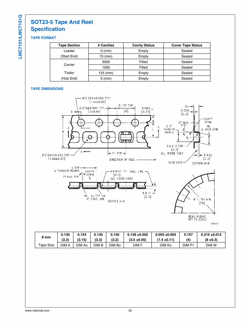
SOT23-5 Tape And Reel
Specification
TAPE FORMAT
Tape Section # Cavities Cavity Status Cover Tape Status
Leader 0 (min) Empty Sealed
(Start End) 75 (min) Empty Sealed
Carrier3000 Filled Sealed
1000 Filled Sealed
Trailer 125 (min) Empty Sealed
(Hub End) 0 (min) Empty Sealed
TAPE DIMENSIONS
1199113
8 mm0.130 0.124 0.130 0.126 0.138 ±0.002 0.055 ±0.004 0.157 0.315 ±0.012
(3.3) (3.15) (3.3) (3.2) (3.5 ±0.05) (1.4 ±0.11) (4) (8 ±0.3)
Tape Size DIM A DIM Ao DIM B DIM Bo DIM F DIM Ko DIM P1 DIM W
www.national.com 20
LM
C7101/L
MC
7101Q

REEL DIMENSIONS
1199114
8 mm7.00 0.059 0.512 0.795 2.165 0.331 + 0.059/−0.000 0.567 W1+ 0.078/−0.039
330.00 1.50 13.00 20.20 55.00 8.40 + 1.50/−0.00 14.40 W1 + 2.00/−1.00
Tape Size A B C D N W1 W2 W3
21 www.national.com
LM
C7101/L
MC
7101Q

Physical Dimensions inches (millimeters) unless otherwise noted
5-Pin SOT23 PackageNS Package Number MF05A
www.national.com 22
LM
C7101/L
MC
7101Q

Notes
23 www.national.com
LM
C7101/L
MC
7101Q

NotesL
MC
7101/L
MC
7101Q
Tin
y L
ow
Po
wer
Op
era
tio
nal A
mp
lifi
er
wit
h R
ail-t
o-R
ail In
pu
t an
d O
utp
ut
For more National Semiconductor product information and proven design tools, visit the following Web sites at:
Products Design Support
Amplifiers www.national.com/amplifiers WEBENCH® Tools www.national.com/webench
Audio www.national.com/audio App Notes www.national.com/appnotes
Clock and Timing www.national.com/timing Reference Designs www.national.com/refdesigns
Data Converters www.national.com/adc Samples www.national.com/samples
Interface www.national.com/interface Eval Boards www.national.com/evalboards
LVDS www.national.com/lvds Packaging www.national.com/packaging
Power Management www.national.com/power Green Compliance www.national.com/quality/green
Switching Regulators www.national.com/switchers Distributors www.national.com/contacts
LDOs www.national.com/ldo Quality and Reliability www.national.com/quality
LED Lighting www.national.com/led Feedback/Support www.national.com/feedback
Voltage Reference www.national.com/vref Design Made Easy www.national.com/easy
PowerWise® Solutions www.national.com/powerwise Solutions www.national.com/solutions
Serial Digital Interface (SDI) www.national.com/sdi Mil/Aero www.national.com/milaero
Temperature Sensors www.national.com/tempsensors SolarMagic™ www.national.com/solarmagic
Wireless (PLL/VCO) www.national.com/wireless PowerWise® DesignUniversity
www.national.com/training
THE CONTENTS OF THIS DOCUMENT ARE PROVIDED IN CONNECTION WITH NATIONAL SEMICONDUCTOR CORPORATION(“NATIONAL”) PRODUCTS. NATIONAL MAKES NO REPRESENTATIONS OR WARRANTIES WITH RESPECT TO THE ACCURACYOR COMPLETENESS OF THE CONTENTS OF THIS PUBLICATION AND RESERVES THE RIGHT TO MAKE CHANGES TOSPECIFICATIONS AND PRODUCT DESCRIPTIONS AT ANY TIME WITHOUT NOTICE. NO LICENSE, WHETHER EXPRESS,IMPLIED, ARISING BY ESTOPPEL OR OTHERWISE, TO ANY INTELLECTUAL PROPERTY RIGHTS IS GRANTED BY THISDOCUMENT.
TESTING AND OTHER QUALITY CONTROLS ARE USED TO THE EXTENT NATIONAL DEEMS NECESSARY TO SUPPORTNATIONAL’S PRODUCT WARRANTY. EXCEPT WHERE MANDATED BY GOVERNMENT REQUIREMENTS, TESTING OF ALLPARAMETERS OF EACH PRODUCT IS NOT NECESSARILY PERFORMED. NATIONAL ASSUMES NO LIABILITY FORAPPLICATIONS ASSISTANCE OR BUYER PRODUCT DESIGN. BUYERS ARE RESPONSIBLE FOR THEIR PRODUCTS ANDAPPLICATIONS USING NATIONAL COMPONENTS. PRIOR TO USING OR DISTRIBUTING ANY PRODUCTS THAT INCLUDENATIONAL COMPONENTS, BUYERS SHOULD PROVIDE ADEQUATE DESIGN, TESTING AND OPERATING SAFEGUARDS.
EXCEPT AS PROVIDED IN NATIONAL’S TERMS AND CONDITIONS OF SALE FOR SUCH PRODUCTS, NATIONAL ASSUMES NOLIABILITY WHATSOEVER, AND NATIONAL DISCLAIMS ANY EXPRESS OR IMPLIED WARRANTY RELATING TO THE SALEAND/OR USE OF NATIONAL PRODUCTS INCLUDING LIABILITY OR WARRANTIES RELATING TO FITNESS FOR A PARTICULARPURPOSE, MERCHANTABILITY, OR INFRINGEMENT OF ANY PATENT, COPYRIGHT OR OTHER INTELLECTUAL PROPERTYRIGHT.
LIFE SUPPORT POLICY
NATIONAL’S PRODUCTS ARE NOT AUTHORIZED FOR USE AS CRITICAL COMPONENTS IN LIFE SUPPORT DEVICES ORSYSTEMS WITHOUT THE EXPRESS PRIOR WRITTEN APPROVAL OF THE CHIEF EXECUTIVE OFFICER AND GENERALCOUNSEL OF NATIONAL SEMICONDUCTOR CORPORATION. As used herein:
Life support devices or systems are devices which (a) are intended for surgical implant into the body, or (b) support or sustain life andwhose failure to perform when properly used in accordance with instructions for use provided in the labeling can be reasonably expectedto result in a significant injury to the user. A critical component is any component in a life support device or system whose failure to performcan be reasonably expected to cause the failure of the life support device or system or to affect its safety or effectiveness.
National Semiconductor and the National Semiconductor logo are registered trademarks of National Semiconductor Corporation. All otherbrand or product names may be trademarks or registered trademarks of their respective holders.
Copyright© 2009 National Semiconductor Corporation
For the most current product information visit us at www.national.com
National SemiconductorAmericas TechnicalSupport CenterEmail: [email protected]: 1-800-272-9959
National Semiconductor EuropeTechnical Support CenterEmail: [email protected]
National Semiconductor AsiaPacific Technical Support CenterEmail: [email protected]
National Semiconductor JapanTechnical Support CenterEmail: [email protected]
www.national.com