Embed Size (px)
Citation preview
LMX2522, LMX2532
www.ti.com SNWS009B –MARCH 2003–REVISED APRIL 2013
LMX2522/LMX2532 PLLatinum™ Frequency Synthesizer System with Integrated VCOsCheck for Samples: LMX2522, LMX2532
1FEATURES DESCRIPTIONLMX2522 and LMX2532 are highly integrated, high
23• Small Sizeperformance, low power frequency synthesizer
– Small 5.0 mm x 5.0 mm x 0.75 mm 28-Pin systems optimized for Korean PCS (K-PCS) withWQFN Package GPS and Korean Cellular (K-Cellular) with GPS,
• RF/GPS Synthesizer System CDMA (1xRTT, IS-95) mobile handsets. Using aproprietary digital phase locked loop technique,– Integrated RF VCOLMX2522 and LMX2532 generate very stable, low
– Integrated GPS VCO noise local oscillator signals for up and down– Integrated Loop Filter conversion in wireless communications devices.– Low Spurious, Low Phase Noise Fractional- LMX2522 and LMX2532 include a RF voltage
N RF PLL Based on 11-bit Delta Sigma controlled oscillator (VCO), a GPS VCO, a loop filter,Modulator and a fractional-N RF PLL based on a delta sigma
modulator. In concert these blocks form a closed loop– 10 kHz Frequency ResolutionRF and GPS synthesizer system. LMX2522 supports• IF Synthesizer Systemthe Korean PCS band with GPS and LMX2532
– Integer-N IF PLL supports the Korean Cellular band with GPS.– Programmable Charge Pump Current LMX2522 and LMX2532 include an Integer-N IF PLL
Levels also. For more flexible loop filter designs, the IF PLL– Programmable Frequencies includes a 4-level programmable charge pump.
Together with an external VCO and loop filter,• Supports Various Reference OscillatorLMX2522 and LMX2532 make a complete closedFrequenciesloop IF synthesizer system.
– 19.20/19.68 MHzSerial data is transferred to the device via a three-• Fast Lock Time: 500 µswire MICROWIRE interface (DATA, LE, CLK).
• Low Current ConsumptionOperating supply voltage ranges from 2.7 V to 3.3 V.– 17 mA at 2.8 VLMX2502 and LMX2512 feature low current
• 2.7 V to 3.3 V Operation consumption: 17 mA at 2.8 V.• Digital Filtered Lock Detect Output LMX2522 and LMX2532 are available in a 28-pin• Hardware and Software Power Down Control WQFN package.
APPLICATIONS• Korean PCS CDMA Systems with GPS• Korean Cellular CDMA Systems with GPS
1
Please be aware that an important notice concerning availability, standard warranty, and use in critical applications ofTexas Instruments semiconductor products and disclaimers thereto appears at the end of this data sheet.
2PLLatinum is a trademark of Texas Instruments.3All other trademarks are the property of their respective owners.
PRODUCTION DATA information is current as of publication date. Copyright © 2003–2013, Texas Instruments IncorporatedProducts conform to specifications per the terms of the TexasInstruments standard warranty. Production processing does notnecessarily include testing of all parameters.
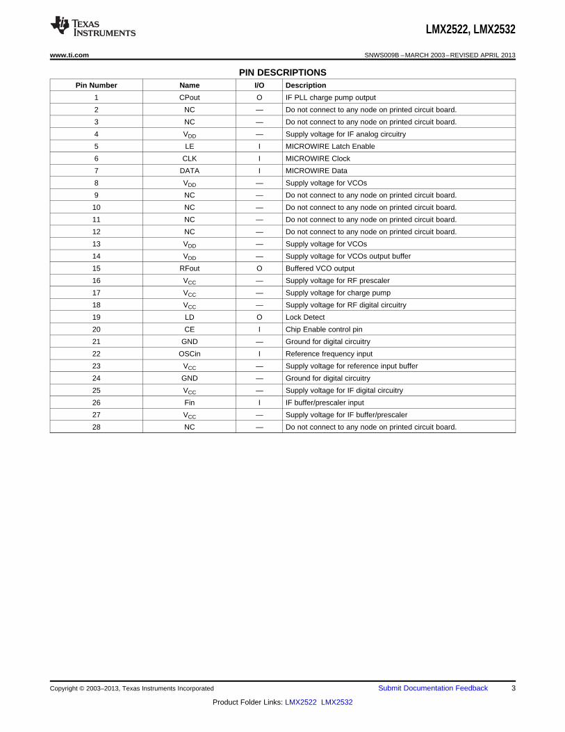
CPout
14
NC
NC
NC
VDD
NC
NC
LE
NC
CLK
DATA
VD
D
15
GND
OS
Cin
CE
LD
VCC
RFoutGND
VC
C
VC
C
GND
VC
C
Fin
NC
13
12
11
1098
16
17
21
20
19
18
1
2
3
4
5
6
7
22
23
24
25
26
27
28
VCC
VCC
VD
D
VD
D
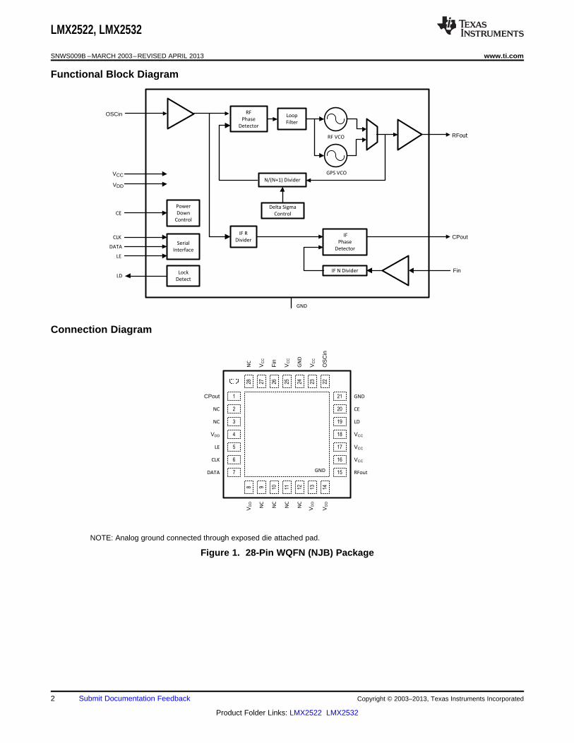
RF
Phase
Detector
Loop
Filter
N/(N+1) Divider
Delta Sigma
Control
RFout
Fin
OSCin
IF N Divider
IF
Phase
Detector
IF R
DividerCPout
RF VCO
GPS VCO
Serial
Interface
Power
Down
Control
Lock
Detect
CE
VCC
VDD
GND
LD
CLK
LE
DATA
LMX2522, LMX2532
SNWS009B –MARCH 2003–REVISED APRIL 2013 www.ti.com
Functional Block Diagram
Connection Diagram
NOTE: Analog ground connected through exposed die attached pad.
Figure 1. 28-Pin WQFN (NJB) Package
2 Submit Documentation Feedback Copyright © 2003–2013, Texas Instruments Incorporated
Product Folder Links: LMX2522 LMX2532
LMX2522, LMX2532
www.ti.com SNWS009B –MARCH 2003–REVISED APRIL 2013
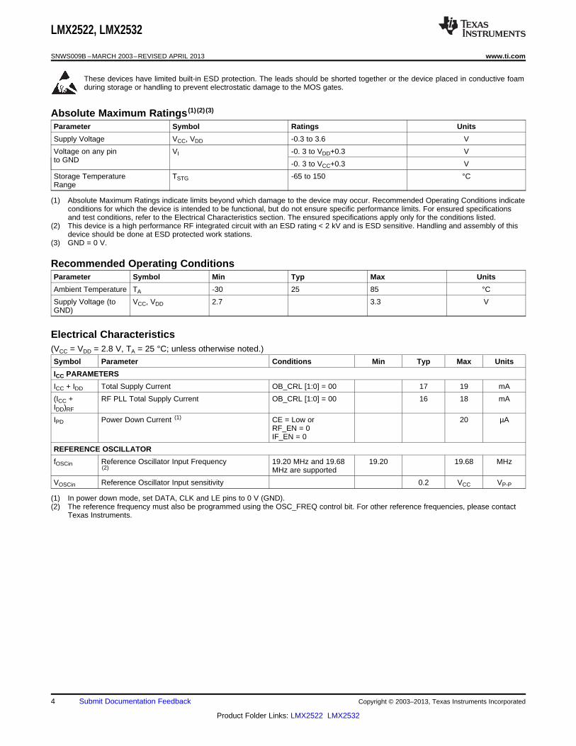
PIN DESCRIPTIONSPin Number Name I/O Description
1 CPout O IF PLL charge pump output
2 NC — Do not connect to any node on printed circuit board.
3 NC — Do not connect to any node on printed circuit board.
4 VDD — Supply voltage for IF analog circuitry
5 LE I MICROWIRE Latch Enable
6 CLK I MICROWIRE Clock
7 DATA I MICROWIRE Data
8 VDD — Supply voltage for VCOs
9 NC — Do not connect to any node on printed circuit board.
10 NC — Do not connect to any node on printed circuit board.
11 NC — Do not connect to any node on printed circuit board.
12 NC — Do not connect to any node on printed circuit board.
13 VDD — Supply voltage for VCOs
14 VDD — Supply voltage for VCOs output buffer
15 RFout O Buffered VCO output
16 VCC — Supply voltage for RF prescaler
17 VCC — Supply voltage for charge pump
18 VCC — Supply voltage for RF digital circuitry
19 LD O Lock Detect
20 CE I Chip Enable control pin
21 GND — Ground for digital circuitry
22 OSCin I Reference frequency input
23 VCC — Supply voltage for reference input buffer
24 GND — Ground for digital circuitry
25 VCC — Supply voltage for IF digital circuitry
26 Fin I IF buffer/prescaler input
27 VCC — Supply voltage for IF buffer/prescaler
28 NC — Do not connect to any node on printed circuit board.
Copyright © 2003–2013, Texas Instruments Incorporated Submit Documentation Feedback 3
Product Folder Links: LMX2522 LMX2532
LMX2522, LMX2532
SNWS009B –MARCH 2003–REVISED APRIL 2013 www.ti.com
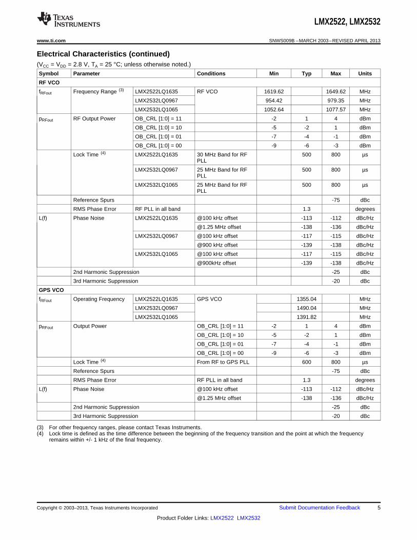
These devices have limited built-in ESD protection. The leads should be shorted together or the device placed in conductive foamduring storage or handling to prevent electrostatic damage to the MOS gates.
Absolute Maximum Ratings (1) (2) (3)
Parameter Symbol Ratings Units
Supply Voltage VCC, VDD -0.3 to 3.6 V
Voltage on any pin VI -0. 3 to VDD+0.3 Vto GND -0. 3 to VCC+0.3 V
Storage Temperature TSTG -65 to 150 °CRange
(1) Absolute Maximum Ratings indicate limits beyond which damage to the device may occur. Recommended Operating Conditions indicateconditions for which the device is intended to be functional, but do not ensure specific performance limits. For ensured specificationsand test conditions, refer to the Electrical Characteristics section. The ensured specifications apply only for the conditions listed.
(2) This device is a high performance RF integrated circuit with an ESD rating < 2 kV and is ESD sensitive. Handling and assembly of thisdevice should be done at ESD protected work stations.
(3) GND = 0 V.
Recommended Operating ConditionsParameter Symbol Min Typ Max Units
Ambient Temperature TA -30 25 85 °C
Supply Voltage (to VCC, VDD 2.7 3.3 VGND)
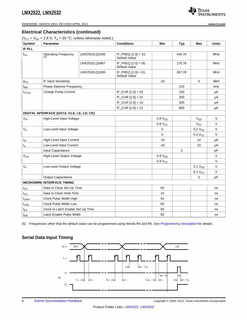
Electrical Characteristics(VCC = VDD = 2.8 V, TA = 25 °C; unless otherwise noted.)
Symbol Parameter Conditions Min Typ Max Units
ICC PARAMETERS
ICC + IDD Total Supply Current OB_CRL [1:0] = 00 17 19 mA
(ICC + RF PLL Total Supply Current OB_CRL [1:0] = 00 16 18 mAIDD)RF
IPD Power Down Current (1) CE = Low or 20 µARF_EN = 0IF_EN = 0
REFERENCE OSCILLATOR
fOSCin Reference Oscillator Input Frequency 19.20 MHz and 19.68 19.20 19.68 MHz(2) MHz are supported
VOSCin Reference Oscillator Input sensitivity 0.2 VCC VP-P
(1) In power down mode, set DATA, CLK and LE pins to 0 V (GND).(2) The reference frequency must also be programmed using the OSC_FREQ control bit. For other reference frequencies, please contact
Texas Instruments.
4 Submit Documentation Feedback Copyright © 2003–2013, Texas Instruments Incorporated
Product Folder Links: LMX2522 LMX2532
LMX2522, LMX2532
www.ti.com SNWS009B –MARCH 2003–REVISED APRIL 2013
Electrical Characteristics (continued)(VCC = VDD = 2.8 V, TA = 25 °C; unless otherwise noted.)
Symbol Parameter Conditions Min Typ Max Units
RF VCO
fRFout Frequency Range (3) LMX2522LQ1635 RF VCO 1619.62 1649.62 MHz
LMX2532LQ0967 954.42 979.35 MHz
LMX2532LQ1065 1052.64 1077.57 MHz
pRFout RF Output Power OB_CRL [1:0] = 11 -2 1 4 dBm
OB_CRL [1:0] = 10 -5 -2 1 dBm
OB_CRL [1:0] = 01 -7 -4 -1 dBm
OB_CRL [1:0] = 00 -9 -6 -3 dBm
Lock Time (4) LMX2522LQ1635 30 MHz Band for RF 500 800 µsPLL
LMX2532LQ0967 25 MHz Band for RF 500 800 µsPLL
LMX2532LQ1065 25 MHz Band for RF 500 800 µsPLL
Reference Spurs -75 dBc
RMS Phase Error RF PLL in all band 1.3 degrees
L(f) Phase Noise LMX2522LQ1635 @100 kHz offset -113 -112 dBc/Hz
@1.25 MHz offset -138 -136 dBc/Hz
LMX2532LQ0967 @100 kHz offset -117 -115 dBc/Hz
@900 kHz offset -139 -138 dBc/Hz
LMX2532LQ1065 @100 kHz offset -117 -115 dBc/Hz
@900kHz offset -139 -138 dBc/Hz
2nd Harmonic Suppression -25 dBc
3rd Harmonic Suppression -20 dBc
GPS VCO
fRFout Operating Frequency LMX2522LQ1635 GPS VCO 1355.04 MHz
LMX2532LQ0967 1490.04 MHz
LMX2532LQ1065 1391.82 MHz
pRFout Output Power OB_CRL [1:0] = 11 -2 1 4 dBm
OB_CRL [1:0] = 10 -5 -2 1 dBm
OB_CRL [1:0] = 01 -7 -4 -1 dBm
OB_CRL [1:0] = 00 -9 -6 -3 dBm
Lock Time (4) From RF to GPS PLL 600 800 µs
Reference Spurs -75 dBc
RMS Phase Error RF PLL in all band 1.3 degrees
L(f) Phase Noise @100 kHz offset -113 -112 dBc/Hz
@1.25 MHz offset -138 -136 dBc/Hz
2nd Harmonic Suppression -25 dBc
3rd Harmonic Suppression -20 dBc
(3) For other frequency ranges, please contact Texas Instruments.(4) Lock time is defined as the time difference between the beginning of the frequency transition and the point at which the frequency
remains within +/- 1 kHz of the final frequency.
Copyright © 2003–2013, Texas Instruments Incorporated Submit Documentation Feedback 5
Product Folder Links: LMX2522 LMX2532
LMX2522, LMX2532
SNWS009B –MARCH 2003–REVISED APRIL 2013 www.ti.com
Electrical Characteristics (continued)(VCC = VDD = 2.8 V, TA = 25 °C; unless otherwise noted.)
Symbol Parameter Conditions Min Typ Max Units
IF PLL
fFin Operating Frequency LMX2522LQ1635 IF_FREQ [1:0] = 10, 440.76 MHz(5) Default Value
LMX2532LQ0967 IF_FREQ [1:0] = 00, 170.76 MHzDefault Value
LMX2532LQ1065 IF_FREQ [1:0] = 01, 367.20 MHzDefault Value
pFin IF Input Sensitivity -10 0 dBm
fΦIF Phase Detector Frequency 120 kHz
ICPout Charge Pump Current IF_CUR [1:0] = 00 100 µA
IF_CUR [1:0] = 01 200 µA
IF_CUR [1:0] = 10 300 µA
IF_CUR [1:0] = 11 800 µA
DIGITAL INTERFACE (DATA, CLK, LE, LD, CE)
VIH High-Level Input Voltage 0.8 VDD VDD V
0.8 VCC VCC V
VIL Low-Level Input Voltage 0 0.2 VDD V
0 0.2 VCC V
IIH High-Level Input Current -10 10 µA
IIL Low-Level Input Current -10 10 µA
Input Capacitance 3 pF
VOH High-Level Output Voltage 0.9 VDD V
0.9 VCC V
VOL Low-Level Output Voltage 0.1 VDD V
0.1 VCC V
Output Capacitance 5 pF
MICROWIRE INTERFACE TIMING
tCS Data to Clock Set Up Time 50 ns
tCH Data to Clock Hold Time 10 ns
tCWH Clock Pulse Width High 50 ns
tCWL Clock Pulse Width Low 50 ns
tES Clock to Latch Enable Set Up Time 50 ns
tEW Latch Enable Pulse Width 50 ns
(5) Frequencies other that the default value can be programmed using Words R4 and R5. See Programming Description for details.
Serial Data Input Timing
6 Submit Documentation Feedback Copyright © 2003–2013, Texas Instruments Incorporated
Product Folder Links: LMX2522 LMX2532
LMX2522, LMX2532
www.ti.com SNWS009B –MARCH 2003–REVISED APRIL 2013
FUNCTIONAL DESCRIPTION
GENERAL DESCRIPTION
LMX2522/32 is a highly integrated frequency synthesizer system that generates LO signals for PCS, CellularCDMA and GPS systems. These devices include all of the functional blocks of a PLL, RF VCO, prescaler, RFphase detector, and loop filter. The need for external components is limited to a few passive elements formatching the output impedance and bypass elements for power line stabilization.
In addition to the RF circuitry, the IC also includes IF frequency dividers, and an IF phase detector to completethe IF synthesis with an external VCO and loop filter. Table 4 summarizes the counter values to generate thedefault IF frequencies.
Using a low spurious fractional-N synthesizer based on a delta sigma modulator, the circuit can support 10 kHzchannel spacing for PCS, Cellular CDMA and GPS systems.
The fractional-N synthesizer enables faster lock time, which reduces power consumption and system set-up time.Additionally, the loop filter occupies a smaller area as opposed to the integer-N architecture. This allows the loopfilter to be embedded into the circuit, minimizing the external noise coupling and total form factor. The deltasigma architecture delivers very low spurious, which can be a significant problem for other PLL solutions.
The circuit also supports commonly used reference frequencies of 19.20 MHz and 19.68 MHz.
FREQUENCY GENERATION
RF-PLL Section
The divide ratio can be calculated using the following equation:
LMX2522 – PCS CDMA:fVCO = {8 x RF_B + RF_A + (RF_FN / fOSC) x 104} x fOSC
where• (RF_A < RF_B)
LMX2532 – Cellular CDMA:fVCO = {6 x RF_B + RF_A + (RF_FN / fOSC) x 104} x fOSC
where• (RF_A < RF_B)• fVCO: Output frequency of voltage controlled oscillator (VCO)• RF_B: Preset divide ratio of binary 4-bit programmable counter (2 ≤ RF_B ≤ 15)• RF_A: Preset divide ratio of binary 3-bit swallow counter (0 ≤ RF_A ≤ 7 for LMX2522 or 0 ≤ RF_A ≤ 5 for
LMX2532)• RF_FN: Preset numerator of binary 11-bit modulus counter (0 ≤ RF_FN < 1920 for fOSC = 19.20 MHz or 0 ≤
RF_FN < 1968 for fOSC = 19.68 MHz)• fOSC: Reference oscillator frequency
Copyright © 2003–2013, Texas Instruments Incorporated Submit Documentation Feedback 7
Product Folder Links: LMX2522 LMX2532
LMX2522, LMX2532
SNWS009B –MARCH 2003–REVISED APRIL 2013 www.ti.com
GPS-PLL SECTION
The divide ratio can be calculated using the following equation:
LMX2522 – PCS CDMA:fVCO = {6 x RF_B + RF_A + (RF_FN / fOSC) x 104} x fOSC
where• (RF_A < RF_B)
LMX2532 – Cellular CDMA:fVCO = {8 x RF_B + RF_A + (RF_FN / fOSC) x 104} x fOSC
where• (RF_A < RF_B)• fVCO: Output frequency of voltage controlled oscillator (VCO)• RF_B: Preset divide ratio of binary 4-bit programmable counter (2 ≤ RF_B ≤ 15)• RF_A: Preset divide ratio of binary 3-bit swallow counter (0 ≤ RF_A ≤ 5 for LMX2522 or 0 ≤ RF_A ≤ 7 for
LMX2532)• RF_FN: Preset numerator of binary 11-bit modulus counter (0 ≤ RF_FN < 1920 for fOSC = 19.20 MHz or 0 ≤
RF_FN < 1968 for fOSC = 19.68 MHz)• fOSC: Reference oscillator frequency
PCS CDMA applications using the LMX2522, if the GPS frequency is 1355.04 MHz, Table 1 provides the properregister settings:
Table 1. Settings for GPS (1355.04 MHz) in LMX2522 PCS CDMA application
Reference Frequency RF_B RF_A RF_FN
19.20 MHz 11 4 1104
19.68 MHz 11 2 1680
Cellular CDMA applications using the LMX2532, in which the GPS frequency is 1490.04 MHz, then Table 2provides the proper register settings:
Table 2. Settings for GPS (1490.04 MHz) in LMX2532 Cellular CDMA application
Reference Frequency RF_B RF_A RF_FN
19.20 MHz 9 5 1164
19.68 MHz 9 3 1404
Cellular CDMA applications using the LMX2532, in which the GPS frequency is 1391.82 MHz, then Table 3provides the proper register settings:
Table 3. Settings for GPS (1391.82 MHz) in LMX2532 Cellular CDMA application
Reference Frequency RF_B RF_A RF_FN
19.20 MHz 9 0 942
19.68 MHz 8 6 1422
8 Submit Documentation Feedback Copyright © 2003–2013, Texas Instruments Incorporated
Product Folder Links: LMX2522 LMX2532

LMX2522, LMX2532
www.ti.com SNWS009B –MARCH 2003–REVISED APRIL 2013
IF-PLL SECTIONfVCO = {16 x IF_B + IF_A} x fOSC / IF_R
where• (IF_A < IF_B)• fVCO: Output frequency of the voltage controlled oscillator (VCO)• IF_B: Preset divide ratio of the binary 9-bit programmable counter (1 ≤ IF_B ≤ 511)• IF_A: Preset divide ratio of the binary 4-bit swallow counter (0 ≤ IF_A ≤ 15)• fOSC: Reference oscillator frequency• IF_R: Preset divide ratio of the binary 9-bit programmable reference counter (2 ≤ IF_R ≤ 511)
From the above equation, the LMX2522/32 generates the fixed IF frequencies as summarized in Table 4.
Table 4. IF Frequencies
Device Type fVCO IF_B IF_A fOSC/IF_R(MHz) (kHz)
LMX2522LQ1635 440.76 229 9 120
LMX2532LQ0967 170.67 88 15 120
LMX2532LQ1065 367.20 191 4 120
VCO FREQUENCY TUNING
The center frequency of the RF VCO is mainly determined by the resonant frequency of the tank circuit. Thistank circuit is implemented on-chip and requires no external inductor. The LMX2522/32 actively tunes the tankcircuit to the required frequency with the built-in tracking algorithm.
BANDWIDTH CONTROL AND FREQUENCY LOCK
During the frequency acquisition period, the loop bandwidth is significantly extended to achieve frequency lock.Once frequency lock occurs, the PLL will return to a steady state condition with the loop bandwidth set to itsnominal value. The transition between acquisition and lock modes occurs seamlessly and extremely fast,thereby, meeting the stringent requirements associated with lock time and phase noise. Several controls(BW_DUR, BW_CRL and BW_EN) are used to optimize the lock time performance.
SPURIOUS REDUCTION
To improve the spurious performance of the device one of two types of spurious reduction schemes can beselected:• A continuous optimization scheme, which tracks the environmental and voltage variations, giving the best
spurious performance over changing conditions• A one time optimization scheme, which sets the internal compensation values only when the PLL goes into a
locked state.
The spurious reduction can also be disabled, but it is recommended that the continuous optimization mode beused for normal operation.
Copyright © 2003–2013, Texas Instruments Incorporated Submit Documentation Feedback 9
Product Folder Links: LMX2522 LMX2532
fR/64
LD
't > tW1 't > tW2
fN/64
LMX2522, LMX2532
SNWS009B –MARCH 2003–REVISED APRIL 2013 www.ti.com
POWER DOWN MODE
The LMX2522 and LMX2532 include a power down mode to reduce the power consumption. The LMX2522/32enters into the power down mode either by taking the CE pin LOW or by setting the power down bits in RegisterR1. Table 5 summarizes the power down function. If CE is set LOW, the circuit is powered down regardless ofthe register values. When CE is HIGH, the IF and RF circuitry are individually powered down by setting theregister bits.
Table 5. Power Down Configuration (1)
CE Pin RF_EN IF_EN RF Circuitry IF Circuitry
0 X X OFF OFF
1 0 0 OFF OFF
1 0 1 OFF ON
1 1 0 ON OFF
1 1 1 ON ON
(1) X = Don’t care.
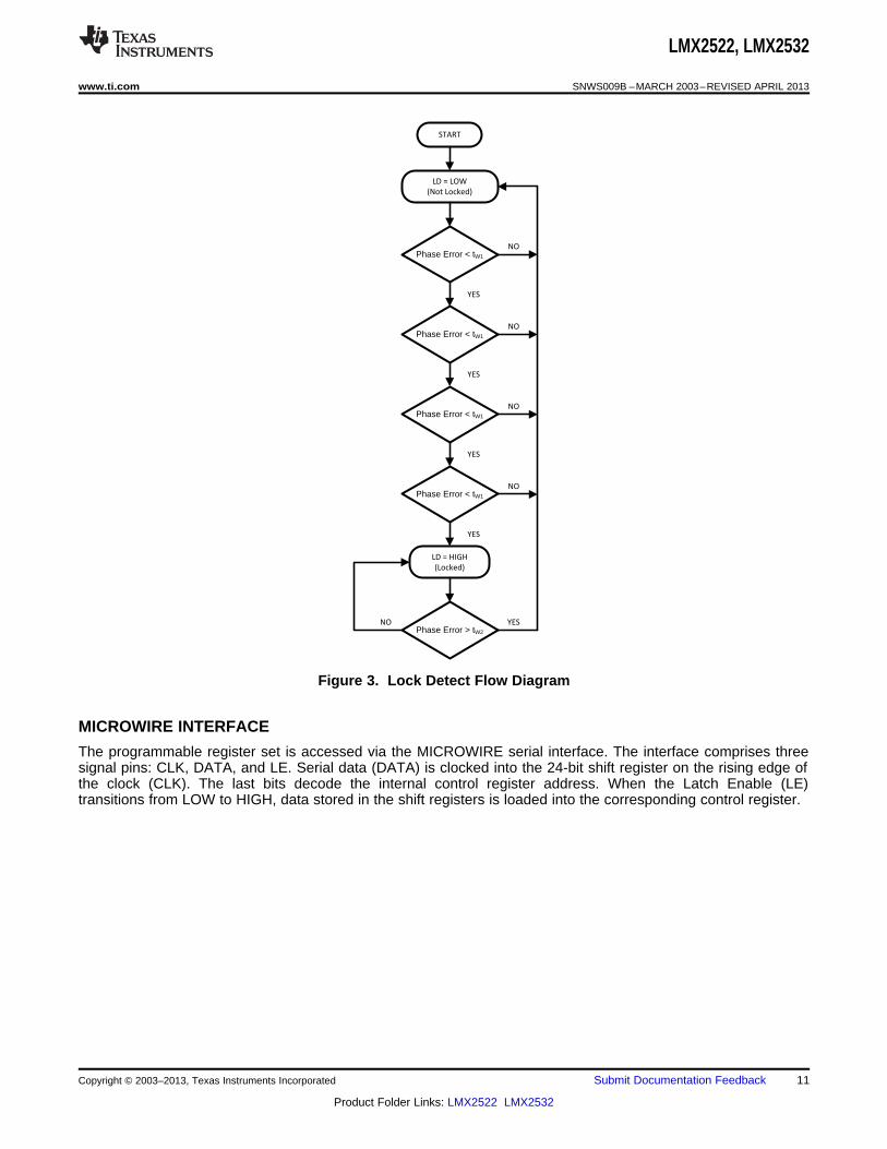
LOCK DETECT
The LD output can be used to indicate the lock status of the RF PLL. Bit 21 in Register R0 determines the signalthat appears on the LD pin. When the RF PLL is not locked, the LD pin remains LOW. After obtaining phaselock, the LD pin will have a logical HIGH level. The output can also be programmed to be ground at all times.
Table 6. Lock Detect Modes
LD Bit Mode
0 Disable (GND)
1 Enable
Table 7. Lock Detect Logic Table (1) (2) (3) (4) (5)
RF PLL Section LD Output
Locked HIGH
Not Locked LOW
(1) LD output becomes low when the phase error is larger than tW2.(2) LD output becomes high when the phase error is less than tW1 for four or more consecutive cycles.(3) Phase Error is measured on leading edge. Only errors greater than tW1 and tW2 are labeled.(4) tW1 and tW2 are equal to 10 ns.(5) The lock detect comparison occurs with every 64th cycle of fR and fN.
Figure 2. Lock Detect Timing Diagram Waveform
10 Submit Documentation Feedback Copyright © 2003–2013, Texas Instruments Incorporated
Product Folder Links: LMX2522 LMX2532
NO
NO
NO
YES
YES
YES
Phase Error < tW1
LD = LOW
(Not Locked)
Phase Error < tW1
Phase Error < tW1
LD = HIGH
(Locked)
Phase Error < tW1
Phase Error > tW2
YES
NO
NO
YES
START
LMX2522, LMX2532
www.ti.com SNWS009B –MARCH 2003–REVISED APRIL 2013
Figure 3. Lock Detect Flow Diagram
MICROWIRE INTERFACE
The programmable register set is accessed via the MICROWIRE serial interface. The interface comprises threesignal pins: CLK, DATA, and LE. Serial data (DATA) is clocked into the 24-bit shift register on the rising edge ofthe clock (CLK). The last bits decode the internal control register address. When the Latch Enable (LE)transitions from LOW to HIGH, data stored in the shift registers is loaded into the corresponding control register.
Copyright © 2003–2013, Texas Instruments Incorporated Submit Documentation Feedback 11
Product Folder Links: LMX2522 LMX2532
LMX2522, LMX2532
SNWS009B –MARCH 2003–REVISED APRIL 2013 www.ti.com
Programming Description
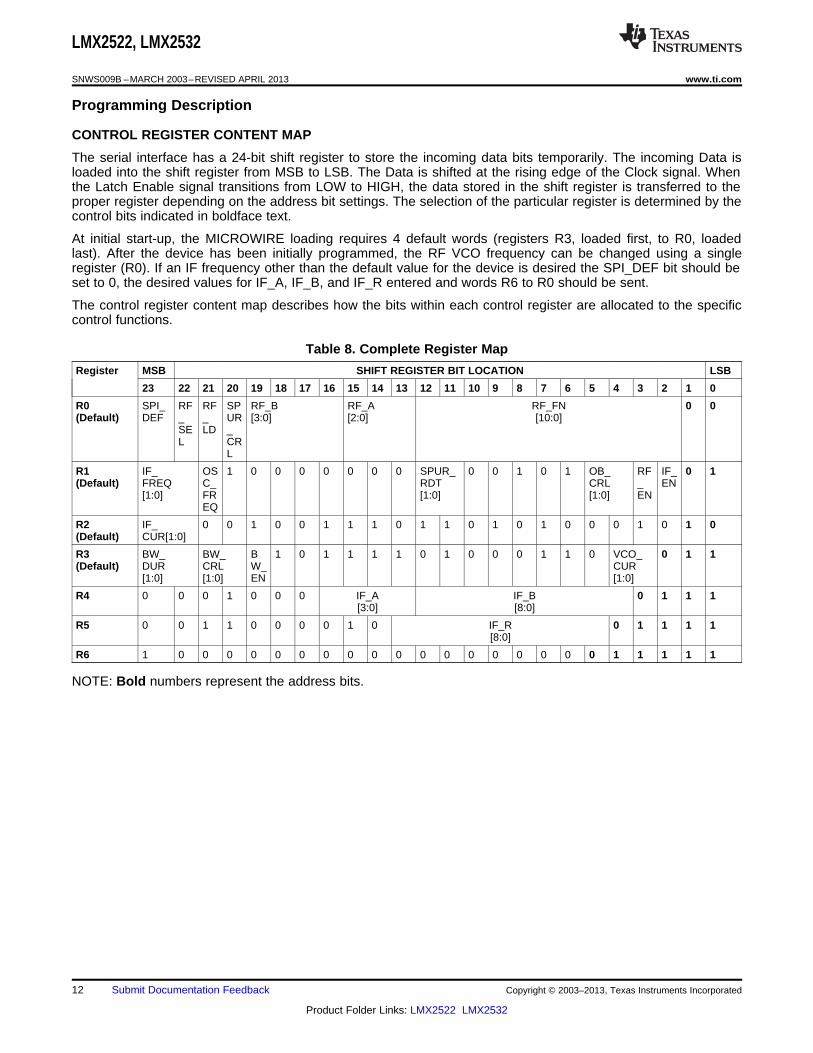
CONTROL REGISTER CONTENT MAP
The serial interface has a 24-bit shift register to store the incoming data bits temporarily. The incoming Data isloaded into the shift register from MSB to LSB. The Data is shifted at the rising edge of the Clock signal. Whenthe Latch Enable signal transitions from LOW to HIGH, the data stored in the shift register is transferred to theproper register depending on the address bit settings. The selection of the particular register is determined by thecontrol bits indicated in boldface text.
At initial start-up, the MICROWIRE loading requires 4 default words (registers R3, loaded first, to R0, loadedlast). After the device has been initially programmed, the RF VCO frequency can be changed using a singleregister (R0). If an IF frequency other than the default value for the device is desired the SPI_DEF bit should beset to 0, the desired values for IF_A, IF_B, and IF_R entered and words R6 to R0 should be sent.
The control register content map describes how the bits within each control register are allocated to the specificcontrol functions.
Table 8. Complete Register Map
Register MSB SHIFT REGISTER BIT LOCATION LSB
23 22 21 20 19 18 17 16 15 14 13 12 11 10 9 8 7 6 5 4 3 2 1 0
R0 SPI_ RF RF SP RF_B RF_A RF_FN 0 0(Default) DEF _ _ UR [3:0] [2:0] [10:0]
SE LD _L CR
L
R1 IF_ OS 1 0 0 0 0 0 0 0 SPUR_ 0 0 1 0 1 OB_ RF IF_ 0 1(Default) FREQ C_ RDT CRL _ EN
[1:0] FR [1:0] [1:0] ENEQ
R2 IF_ 0 0 1 0 0 1 1 1 0 1 1 0 1 0 1 0 0 0 1 0 1 0(Default) CUR[1:0]
R3 BW_ BW_ B 1 0 1 1 1 1 0 1 0 0 0 1 1 0 VCO_ 0 1 1(Default) DUR CRL W_ CUR
[1:0] [1:0] EN [1:0]
R4 0 0 0 1 0 0 0 IF_A IF_B 0 1 1 1[3:0] [8:0]
R5 0 0 1 1 0 0 0 0 1 0 IF_R 0 1 1 1 1[8:0]
R6 1 0 0 0 0 0 0 0 0 0 0 0 0 0 0 0 0 0 0 1 1 1 1 1
NOTE: Bold numbers represent the address bits.
12 Submit Documentation Feedback Copyright © 2003–2013, Texas Instruments Incorporated
Product Folder Links: LMX2522 LMX2532
LMX2522, LMX2532
www.ti.com SNWS009B –MARCH 2003–REVISED APRIL 2013
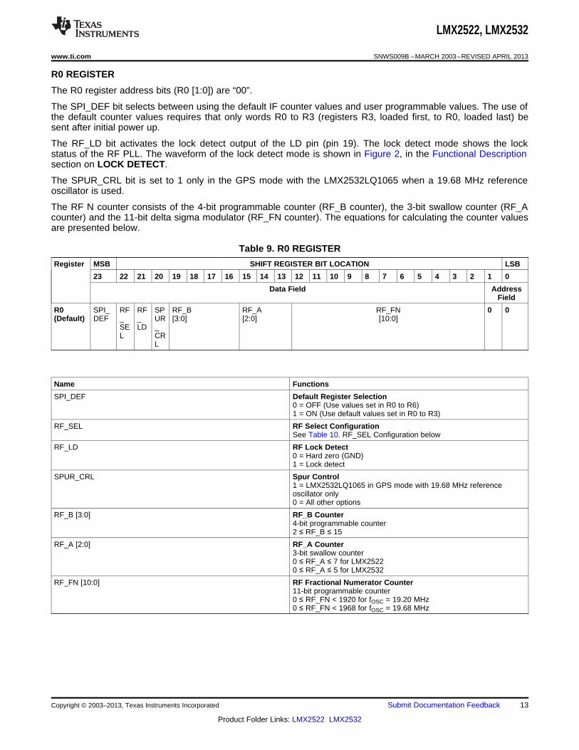
R0 REGISTER
The R0 register address bits (R0 [1:0]) are “00”.
The SPI_DEF bit selects between using the default IF counter values and user programmable values. The use ofthe default counter values requires that only words R0 to R3 (registers R3, loaded first, to R0, loaded last) besent after initial power up.
The RF_LD bit activates the lock detect output of the LD pin (pin 19). The lock detect mode shows the lockstatus of the RF PLL. The waveform of the lock detect mode is shown in Figure 2, in the Functional Descriptionsection on LOCK DETECT.
The SPUR_CRL bit is set to 1 only in the GPS mode with the LMX2532LQ1065 when a 19.68 MHz referenceoscillator is used.
The RF N counter consists of the 4-bit programmable counter (RF_B counter), the 3-bit swallow counter (RF_Acounter) and the 11-bit delta sigma modulator (RF_FN counter). The equations for calculating the counter valuesare presented below.
Table 9. R0 REGISTER
Register MSB SHIFT REGISTER BIT LOCATION LSB
23 22 21 20 19 18 17 16 15 14 13 12 11 10 9 8 7 6 5 4 3 2 1 0
Data Field AddressField
R0 SPI_ RF RF SP RF_B RF_A RF_FN 0 0(Default) DEF _ _ UR [3:0] [2:0] [10:0]
SE LD _L CR
L
Name Functions
SPI_DEF Default Register Selection0 = OFF (Use values set in R0 to R6)1 = ON (Use default values set in R0 to R3)
RF_SEL RF Select ConfigurationSee Table 10. RF_SEL Configuration below
RF_LD RF Lock Detect0 = Hard zero (GND)1 = Lock detect
SPUR_CRL Spur Control1 = LMX2532LQ1065 in GPS mode with 19.68 MHz referenceoscillator only0 = All other options
RF_B [3:0] RF_B Counter4-bit programmable counter2 ≤ RF_B ≤ 15
RF_A [2:0] RF_A Counter3-bit swallow counter0 ≤ RF_A ≤ 7 for LMX25220 ≤ RF_A ≤ 5 for LMX2532
RF_FN [10:0] RF Fractional Numerator Counter11-bit programmable counter0 ≤ RF_FN < 1920 for fOSC = 19.20 MHz0 ≤ RF_FN < 1968 for fOSC = 19.68 MHz
Copyright © 2003–2013, Texas Instruments Incorporated Submit Documentation Feedback 13
Product Folder Links: LMX2522 LMX2532
LMX2522, LMX2532
SNWS009B –MARCH 2003–REVISED APRIL 2013 www.ti.com
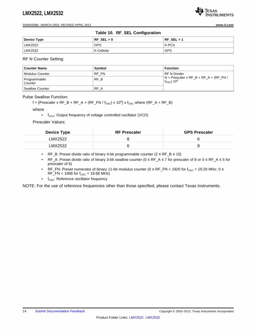
Table 10. RF_SEL Configuration
Device Type RF_SEL = 0 RF_SEL = 1
LMX2522 GPS K-PCS
LMX2532 K-Cellular GPS
RF N Counter Setting:
Counter Name Symbol Function
Modulus Counter RF_FN RF N DividerN = Prescaler x RF_B + RF_A + (RF_FN /Programmable RF_BfOSC) 104
Counter
Swallow Counter RF_A
Pulse Swallow Function:f = {Prescaler x RF_B + RF_A + (RF_FN / fOSC) x 104} x fOSC where (RF_A < RF_B)
where• fVCO: Output frequency of voltage controlled oscillator (VCO)
Prescaler Values:
Device Type RF Prescaler GPS Prescaler
LMX2522 8 6
LMX2532 6 8
• RF_B: Preset divide ratio of binary 4-bit programmable counter (2 ≤ RF_B ≤ 15)• RF_A: Preset divide ratio of binary 3-bit swallow counter (0 ≤ RF_A ≤ 7 for prescaler of 8 or 0 ≤ RF_A ≤ 5 for
prescaler of 6)• RF_FN: Preset numerator of binary 11-bit modulus counter (0 ≤ RF_FN < 1920 for fOSC = 19.20 MHz; 0 ≤
RF_FN < 1968 for fOSC = 19.68 MHz)• fOSC: Reference oscillator frequency
NOTE: For the use of reference frequencies other than those specified, please contact Texas Instruments.
14 Submit Documentation Feedback Copyright © 2003–2013, Texas Instruments Incorporated
Product Folder Links: LMX2522 LMX2532
LMX2522, LMX2532
www.ti.com SNWS009B –MARCH 2003–REVISED APRIL 2013
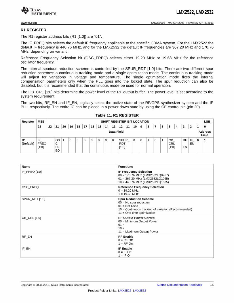
R1 REGISTER
The R1 register address bits (R1 [1:0]) are “01”.
The IF_FREQ bits selects the default IF frequency applicable to the specific CDMA system. For the LMX2522 thedefault IF frequency is 440.76 MHz, and for the LMX2532 the default IF frequencies are 367.20 MHz and 170.76MHz, depending on variant.
Reference Frequency Selection bit (OSC_FREQ) selects either 19.20 MHz or 19.68 MHz for the referenceoscillator frequency.
The internal spurious reduction scheme is controlled by the SPUR_RDT [1:0] bits. There are two different spurreduction schemes: a continuous tracking mode and a single optimization mode. The continuous tracking modewill adjust for variations in voltage and temperature. The single optimization mode fixes the internalcompensation parameters only when the PLL goes into the locked state. The spur reduction can also bedisabled, but it is recommended that the continuous mode be used for normal operation.
The OB_CRL [1:0] bits determine the power level of the RF output buffer. The power level is set according to thesystem requirement.
The two bits, RF_EN and IF_EN, logically select the active state of the RF/GPS synthesizer system and the IFPLL, respectively. The entire IC can be placed in a power down state by using the CE control pin (pin 20).
Table 11. R1 REGISTER
Register MSB SHIFT REGISTER BIT LOCATION LSB
23 22 21 20 19 18 17 16 15 14 13 12 11 10 9 8 7 6 5 4 3 2 1 0
Data Field AddressField
R1 IF_ OS 1 0 0 0 0 0 0 0 SPUR_ 0 0 1 0 1 OB_ RF IF_ 0 1(Default) FREQ C_ RDT CRL _ EN
[1:0] FR [1:0] [1:0] ENEQ
Name Functions
IF_FREQ [1:0] IF Frequency Selection00 = 170.76 MHz (LMX2532LQ0967)01 = 367.20 MHz (LMX2532LQ1065)10 = 440.76 MHz (LMX2522LQ1635)
OSC_FREQ Reference Frequency Selection0 = 19.20 MHz1 = 19.68 MHz
SPUR_RDT [1:0] Spur Reduction Scheme00 = No spur reduction01 = Not Used10 = Continuous tracking of variation (Recommended)11 = One time optimization
OB_CRL [1:0] RF Output Power Control00 = Minimum Output Power01 =10 =11 = Maximum Output Power
RF_EN RF Enable0 = RF Off1 = RF On
IF_EN IF Enable0 = IF Off1 = IF On
Copyright © 2003–2013, Texas Instruments Incorporated Submit Documentation Feedback 15
Product Folder Links: LMX2522 LMX2532
LMX2522, LMX2532
SNWS009B –MARCH 2003–REVISED APRIL 2013 www.ti.com
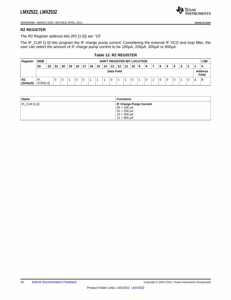
R2 REGISTER
The R2 Register address bits (R2 [1:0]) are “10”.
The IF_CUR [1:0] bits program the IF charge pump current. Considering the external IF VCO and loop filter, theuser can select the amount of IF charge pump current to be 100µA, 200µA, 300µA or 800µA.
Table 12. R2 REGISTER
Register MSB SHIFT REGISTER BIT LOCATION LSB
23 22 21 20 19 18 17 16 15 14 13 12 11 10 9 8 7 6 5 4 3 2 1 0
Data Field AddressField
R2 IF_ 0 0 1 0 0 1 1 1 0 1 1 0 1 0 1 0 0 0 1 0 1 0(Default) CUR[1:0]
Name Functions
IF_CUR [1:0] IF Charge Pump Current00 = 100 µA01 = 200 µA10 = 300 µA11 = 800 µA
16 Submit Documentation Feedback Copyright © 2003–2013, Texas Instruments Incorporated
Product Folder Links: LMX2522 LMX2532
LMX2522, LMX2532
www.ti.com SNWS009B –MARCH 2003–REVISED APRIL 2013
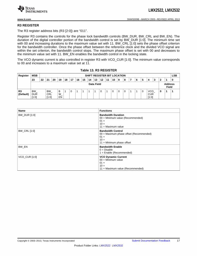
R3 REGISTER
The R3 register address bits (R3 [2:0]) are “011”.
Register R3 contains the controls for the phase lock bandwidth controls (BW_DUR, BW_CRL and BW_EN). Theduration of the digital controller portion of the bandwidth control is set by BW_DUR [1:0]. The minimum time setwith 00 and increasing durations to the maximum value set with 11. BW_CRL [1:0] sets the phase offset criterionfor the bandwidth controller. Once the phase offset between the reference clock and the divided VCO signal arewithin the set criterion, the bandwidth control stops. The maximum phase offset is set with 00 and decreases tothe minimum value set with 11. BW_EN enables the bandwidth control in the locking state.
The VCO dynamic current is also controlled in register R3 with VCO_CUR [1:0]. The minimum value correspondsto 00 and increases to a maximum value set at 11.
Table 13. R3 REGISTER
Register MSB SHIFT REGISTER BIT LOCATION LSB
23 22 21 20 19 18 17 16 15 14 13 12 11 10 9 8 7 6 5 4 3 2 1 0
Data Field AddressField
R3 BW_ BW_ B 1 0 1 1 1 1 0 1 0 0 0 1 1 0 VCO_ 0 1 1(Default) DUR CRL W_ CUR
[1:0] [1:0] EN [1:0]
Name Functions
BW_DUR [1:0] Bandwidth Duration00 = Minimum value (Recommended)01 =10 =11 = Maximum value
BW_CRL [1:0] Bandwidth Control00 = Maximum phase offset (Recommended)01 =10 =11 = Minimum phase offset
BW_EN Bandwidth Enable0 = Disable1 = Enable (Recommended)
VCO_CUR [1:0] VCO Dynamic Current00 = Minimum value01 =10 =11 = Maximum value (Recommended)
Copyright © 2003–2013, Texas Instruments Incorporated Submit Documentation Feedback 17
Product Folder Links: LMX2522 LMX2532
LMX2522, LMX2532
SNWS009B –MARCH 2003–REVISED APRIL 2013 www.ti.com
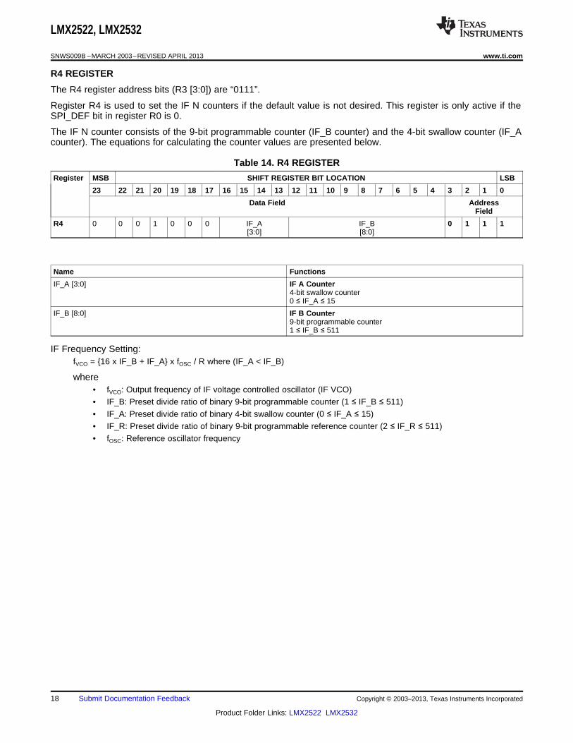
R4 REGISTER
The R4 register address bits (R3 [3:0]) are “0111”.
Register R4 is used to set the IF N counters if the default value is not desired. This register is only active if theSPI_DEF bit in register R0 is 0.
The IF N counter consists of the 9-bit programmable counter (IF_B counter) and the 4-bit swallow counter (IF_Acounter). The equations for calculating the counter values are presented below.
Table 14. R4 REGISTER
Register MSB SHIFT REGISTER BIT LOCATION LSB
23 22 21 20 19 18 17 16 15 14 13 12 11 10 9 8 7 6 5 4 3 2 1 0
Data Field AddressField
R4 0 0 0 1 0 0 0 IF_A IF_B 0 1 1 1[3:0] [8:0]
Name Functions
IF_A [3:0] IF A Counter4-bit swallow counter0 ≤ IF_A ≤ 15
IF_B [8:0] IF B Counter9-bit programmable counter1 ≤ IF_B ≤ 511
IF Frequency Setting:fVCO = {16 x IF_B + IF_A} x fOSC / R where (IF_A < IF_B)
where• fVCO: Output frequency of IF voltage controlled oscillator (IF VCO)• IF_B: Preset divide ratio of binary 9-bit programmable counter (1 ≤ IF_B ≤ 511)• IF_A: Preset divide ratio of binary 4-bit swallow counter (0 ≤ IF_A ≤ 15)• IF_R: Preset divide ratio of binary 9-bit programmable reference counter (2 ≤ IF_R ≤ 511)• fOSC: Reference oscillator frequency
18 Submit Documentation Feedback Copyright © 2003–2013, Texas Instruments Incorporated
Product Folder Links: LMX2522 LMX2532
LMX2522, LMX2532
www.ti.com SNWS009B –MARCH 2003–REVISED APRIL 2013
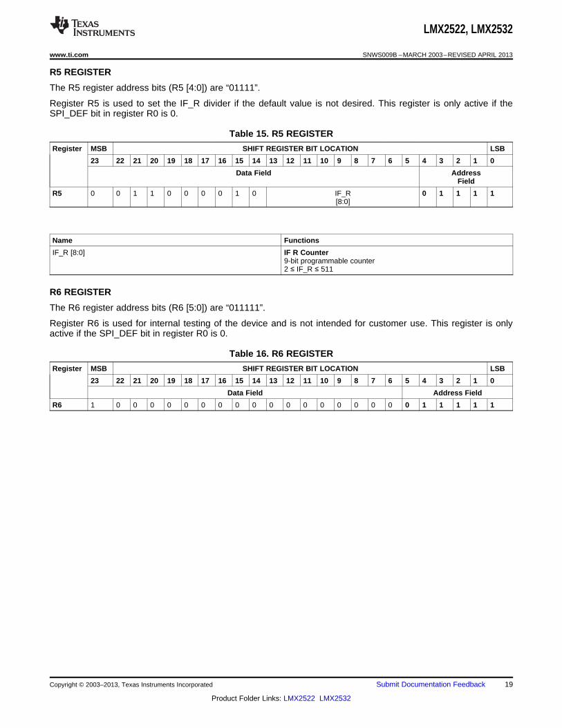
R5 REGISTER
The R5 register address bits (R5 [4:0]) are “01111”.
Register R5 is used to set the IF_R divider if the default value is not desired. This register is only active if theSPI_DEF bit in register R0 is 0.
Table 15. R5 REGISTER
Register MSB SHIFT REGISTER BIT LOCATION LSB
23 22 21 20 19 18 17 16 15 14 13 12 11 10 9 8 7 6 5 4 3 2 1 0
Data Field AddressField
R5 0 0 1 1 0 0 0 0 1 0 IF_R 0 1 1 1 1[8:0]
Name Functions
IF_R [8:0] IF R Counter9-bit programmable counter2 ≤ IF_R ≤ 511
R6 REGISTER
The R6 register address bits (R6 [5:0]) are “011111”.
Register R6 is used for internal testing of the device and is not intended for customer use. This register is onlyactive if the SPI_DEF bit in register R0 is 0.
Table 16. R6 REGISTER
Register MSB SHIFT REGISTER BIT LOCATION LSB
23 22 21 20 19 18 17 16 15 14 13 12 11 10 9 8 7 6 5 4 3 2 1 0
Data Field Address Field
R6 1 0 0 0 0 0 0 0 0 0 0 0 0 0 0 0 0 0 0 1 1 1 1 1
Copyright © 2003–2013, Texas Instruments Incorporated Submit Documentation Feedback 19
Product Folder Links: LMX2522 LMX2532
LMX2522, LMX2532
SNWS009B –MARCH 2003–REVISED APRIL 2013 www.ti.com
REVISION HISTORY
Changes from Revision A (April 2013) to Revision B Page
• Changed layout of National Data Sheet to TI format .......................................................................................................... 19
20 Submit Documentation Feedback Copyright © 2003–2013, Texas Instruments Incorporated
Product Folder Links: LMX2522 LMX2532
PACKAGE OPTION ADDENDUM
www.ti.com 1-Nov-2013
Addendum-Page 1
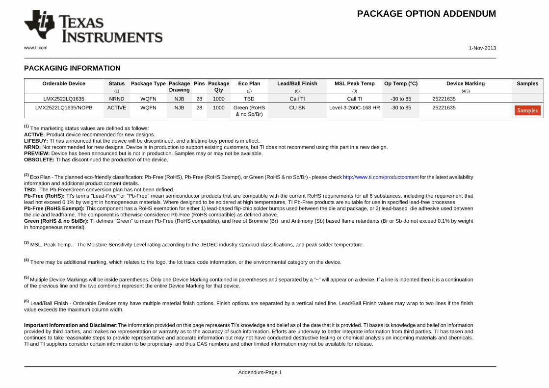
PACKAGING INFORMATION
Orderable Device Status(1)
Package Type PackageDrawing
Pins PackageQty
Eco Plan(2)
Lead/Ball Finish(6)
MSL Peak Temp(3)
Op Temp (°C) Device Marking(4/5)
Samples
LMX2522LQ1635 NRND WQFN NJB 28 1000 TBD Call TI Call TI -30 to 85 25221635
LMX2522LQ1635/NOPB ACTIVE WQFN NJB 28 1000 Green (RoHS& no Sb/Br)
CU SN Level-3-260C-168 HR -30 to 85 25221635
(1) The marketing status values are defined as follows:ACTIVE: Product device recommended for new designs.LIFEBUY: TI has announced that the device will be discontinued, and a lifetime-buy period is in effect.NRND: Not recommended for new designs. Device is in production to support existing customers, but TI does not recommend using this part in a new design.PREVIEW: Device has been announced but is not in production. Samples may or may not be available.OBSOLETE: TI has discontinued the production of the device.
(2) Eco Plan - The planned eco-friendly classification: Pb-Free (RoHS), Pb-Free (RoHS Exempt), or Green (RoHS & no Sb/Br) - please check http://www.ti.com/productcontent for the latest availabilityinformation and additional product content details.TBD: The Pb-Free/Green conversion plan has not been defined.Pb-Free (RoHS): TI's terms "Lead-Free" or "Pb-Free" mean semiconductor products that are compatible with the current RoHS requirements for all 6 substances, including the requirement thatlead not exceed 0.1% by weight in homogeneous materials. Where designed to be soldered at high temperatures, TI Pb-Free products are suitable for use in specified lead-free processes.Pb-Free (RoHS Exempt): This component has a RoHS exemption for either 1) lead-based flip-chip solder bumps used between the die and package, or 2) lead-based die adhesive used betweenthe die and leadframe. The component is otherwise considered Pb-Free (RoHS compatible) as defined above.Green (RoHS & no Sb/Br): TI defines "Green" to mean Pb-Free (RoHS compatible), and free of Bromine (Br) and Antimony (Sb) based flame retardants (Br or Sb do not exceed 0.1% by weightin homogeneous material)
(3) MSL, Peak Temp. - The Moisture Sensitivity Level rating according to the JEDEC industry standard classifications, and peak solder temperature.
(4) There may be additional marking, which relates to the logo, the lot trace code information, or the environmental category on the device.
(5) Multiple Device Markings will be inside parentheses. Only one Device Marking contained in parentheses and separated by a "~" will appear on a device. If a line is indented then it is a continuationof the previous line and the two combined represent the entire Device Marking for that device.
(6) Lead/Ball Finish - Orderable Devices may have multiple material finish options. Finish options are separated by a vertical ruled line. Lead/Ball Finish values may wrap to two lines if the finishvalue exceeds the maximum column width.
Important Information and Disclaimer:The information provided on this page represents TI's knowledge and belief as of the date that it is provided. TI bases its knowledge and belief on informationprovided by third parties, and makes no representation or warranty as to the accuracy of such information. Efforts are underway to better integrate information from third parties. TI has taken andcontinues to take reasonable steps to provide representative and accurate information but may not have conducted destructive testing or chemical analysis on incoming materials and chemicals.TI and TI suppliers consider certain information to be proprietary, and thus CAS numbers and other limited information may not be available for release.
PACKAGE OPTION ADDENDUM
www.ti.com 1-Nov-2013
Addendum-Page 2
In no event shall TI's liability arising out of such information exceed the total purchase price of the TI part(s) at issue in this document sold by TI to Customer on an annual basis.
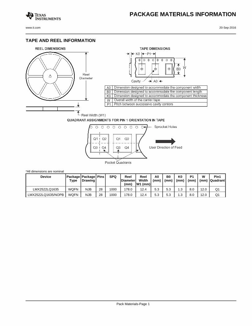
TAPE AND REEL INFORMATION
*All dimensions are nominal
Device PackageType
PackageDrawing
Pins SPQ ReelDiameter
(mm)
ReelWidth
W1 (mm)
A0(mm)
B0(mm)
K0(mm)
P1(mm)
W(mm)
Pin1Quadrant
LMX2522LQ1635 WQFN NJB 28 1000 178.0 12.4 5.3 5.3 1.3 8.0 12.0 Q1
LMX2522LQ1635/NOPB WQFN NJB 28 1000 178.0 12.4 5.3 5.3 1.3 8.0 12.0 Q1
PACKAGE MATERIALS INFORMATION
www.ti.com 20-Sep-2016
Pack Materials-Page 1
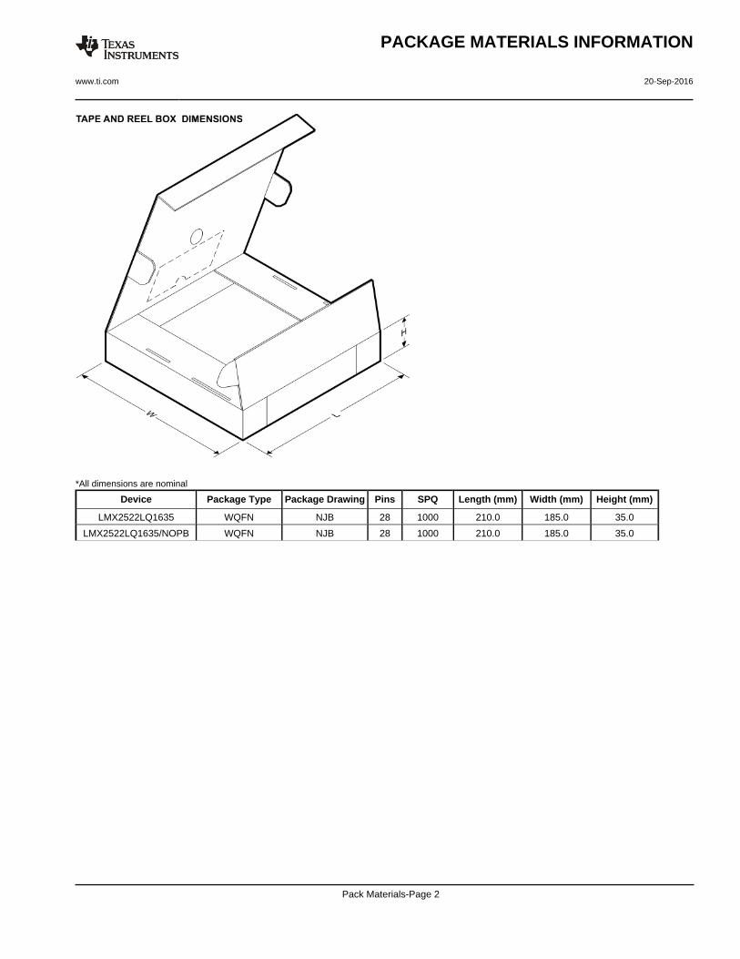
*All dimensions are nominal
Device Package Type Package Drawing Pins SPQ Length (mm) Width (mm) Height (mm)
LMX2522LQ1635 WQFN NJB 28 1000 210.0 185.0 35.0
LMX2522LQ1635/NOPB WQFN NJB 28 1000 210.0 185.0 35.0
PACKAGE MATERIALS INFORMATION
www.ti.com 20-Sep-2016
Pack Materials-Page 2

MECHANICAL DATA
NJB0028A
www.ti.com
LQA28A (REV B)
IMPORTANT NOTICE
Texas Instruments Incorporated and its subsidiaries (TI) reserve the right to make corrections, enhancements, improvements and otherchanges to its semiconductor products and services per JESD46, latest issue, and to discontinue any product or service per JESD48, latestissue. Buyers should obtain the latest relevant information before placing orders and should verify that such information is current andcomplete. All semiconductor products (also referred to herein as “components”) are sold subject to TI’s terms and conditions of salesupplied at the time of order acknowledgment.TI warrants performance of its components to the specifications applicable at the time of sale, in accordance with the warranty in TI’s termsand conditions of sale of semiconductor products. Testing and other quality control techniques are used to the extent TI deems necessaryto support this warranty. Except where mandated by applicable law, testing of all parameters of each component is not necessarilyperformed.TI assumes no liability for applications assistance or the design of Buyers’ products. Buyers are responsible for their products andapplications using TI components. To minimize the risks associated with Buyers’ products and applications, Buyers should provideadequate design and operating safeguards.TI does not warrant or represent that any license, either express or implied, is granted under any patent right, copyright, mask work right, orother intellectual property right relating to any combination, machine, or process in which TI components or services are used. Informationpublished by TI regarding third-party products or services does not constitute a license to use such products or services or a warranty orendorsement thereof. Use of such information may require a license from a third party under the patents or other intellectual property of thethird party, or a license from TI under the patents or other intellectual property of TI.Reproduction of significant portions of TI information in TI data books or data sheets is permissible only if reproduction is without alterationand is accompanied by all associated warranties, conditions, limitations, and notices. TI is not responsible or liable for such altereddocumentation. Information of third parties may be subject to additional restrictions.Resale of TI components or services with statements different from or beyond the parameters stated by TI for that component or servicevoids all express and any implied warranties for the associated TI component or service and is an unfair and deceptive business practice.TI is not responsible or liable for any such statements.Buyer acknowledges and agrees that it is solely responsible for compliance with all legal, regulatory and safety-related requirementsconcerning its products, and any use of TI components in its applications, notwithstanding any applications-related information or supportthat may be provided by TI. Buyer represents and agrees that it has all the necessary expertise to create and implement safeguards whichanticipate dangerous consequences of failures, monitor failures and their consequences, lessen the likelihood of failures that might causeharm and take appropriate remedial actions. Buyer will fully indemnify TI and its representatives against any damages arising out of the useof any TI components in safety-critical applications.In some cases, TI components may be promoted specifically to facilitate safety-related applications. With such components, TI’s goal is tohelp enable customers to design and create their own end-product solutions that meet applicable functional safety standards andrequirements. Nonetheless, such components are subject to these terms.No TI components are authorized for use in FDA Class III (or similar life-critical medical equipment) unless authorized officers of the partieshave executed a special agreement specifically governing such use.Only those TI components which TI has specifically designated as military grade or “enhanced plastic” are designed and intended for use inmilitary/aerospace applications or environments. Buyer acknowledges and agrees that any military or aerospace use of TI componentswhich have not been so designated is solely at the Buyer's risk, and that Buyer is solely responsible for compliance with all legal andregulatory requirements in connection with such use.TI has specifically designated certain components as meeting ISO/TS16949 requirements, mainly for automotive use. In any case of use ofnon-designated products, TI will not be responsible for any failure to meet ISO/TS16949.
Products ApplicationsAudio www.ti.com/audio Automotive and Transportation www.ti.com/automotiveAmplifiers amplifier.ti.com Communications and Telecom www.ti.com/communicationsData Converters dataconverter.ti.com Computers and Peripherals www.ti.com/computersDLP® Products www.dlp.com Consumer Electronics www.ti.com/consumer-appsDSP dsp.ti.com Energy and Lighting www.ti.com/energyClocks and Timers www.ti.com/clocks Industrial www.ti.com/industrialInterface interface.ti.com Medical www.ti.com/medicalLogic logic.ti.com Security www.ti.com/securityPower Mgmt power.ti.com Space, Avionics and Defense www.ti.com/space-avionics-defenseMicrocontrollers microcontroller.ti.com Video and Imaging www.ti.com/videoRFID www.ti-rfid.comOMAP Applications Processors www.ti.com/omap TI E2E Community e2e.ti.comWireless Connectivity www.ti.com/wirelessconnectivity
Mailing Address: Texas Instruments, Post Office Box 655303, Dallas, Texas 75265Copyright © 2016, Texas Instruments Incorporated