Embed Size (px)
Citation preview

Journal of ELECTRICAL ENGINEERING, VOL. 56, NO. 9-10, 2005, 258–264
LOAD CHARACTERISTICS AND CONTROL SYSTEMBEHAVIOURAL MODELLING UNDER OPTIMAL TRAJECTORY
CONTROL OF SERIES RESONANT DC/DC CONVERTERS
Nikolay Bankov∗— Tsvetana Grigorova
∗∗
The paper presents behavioural modelling of the control system of series resonant DC/DC converters operated above theresonant frequency under “optimal trajectory control” technique. This method predicts the fastest response possible with
minimum energy surge in the resonant tank. The steady-state equations described the converter operation above the resonantfrequency as a function of the diode trajectory radius and corresponding normalized load characteristics are proposed. Theyallow evaluating the behaviour of the considered converter when the load is changed strongly during the operation process.Simulation and experimental results are given.
K e y w o r d s: resonant DC/DC converters, control system, optimal trajectory control, behavioural modelling
1 INTRODUCTION
Several control methods of series resonant DC/DCconverters are widely discussed and compared in recentyears [1–6]. Due to the presence of a resonant circuit withits fast transient response, the control of resonant convert-ers is considerably more complex than of PWM converters[1]. The tank processes fast dynamics and exchanges largeamounts of pulsating energy with the source and with theload in each half-cycle of converter operation. The advan-tages of the examined optimal trajectory control methodover the existing methods are a reduced stress on thereactive and power semiconductor switching elements ofthe circuit and a faster response in the case of large varia-tions of circuit operating conditions without affecting theglobal stability of the system [7].
Emphasis in this paper is on obtaining steady stateequations describing the DC/DC resonant converter op-eration above the resonant frequency as a function ofthe diode trajectory radius and corresponding normal-
ized load characteristics, which are useful to design sucha converter. The control system is described using AnalogBehavioural Modelling (ABM) feature provided in OrCadPSpice [8].
2 ANALYSIS AND LOAD CHARACTERISTICSOF THE RESONANT DC/DC CONVERTER
Figure 1 shows the proposed DC/DC converter. Theconverter is operated above the resonant frequency.
Analysis is made under the following assumptions: theconverter elements are ideal; the effect of snubber capac-itors and the ripples of input and output voltages areneglected; the output capacitor is sufficiently large suchthat the output voltage U0 remains constant through aswitching cycle.
The following common symbols are used:
ω0 = 1/√
LC — angular resonant frequency; Z0 =√
L/C — characteristic impedance; ω — switching fre-
Fig. 1. Full-bridge DC/DC resonant converter.
∗University of Food Technologies, Department of Electronics, 26 Maritza Blvd., 4002 Plovdiv, Bulgaria, nikolay [email protected]
∗∗Technical University of Sofia, Branch Plovdiv, Department of Electronics, 61 Sankt Petersburg Blvd., 4000 Plovdiv, Bulgaria,
ISSN 1335-3632 c© 2005 FEI STU

Journal of ELECTRICAL ENGINEERING 56, NO. 9–10, 2005 259
quency; i′(0) = I ′L0 , u′(0) = U ′
C0 — normalized initialvalues of the resonant link current and voltage across se-ries capacitor for each stage of the converter operation;ΘQ = ω0tQ — transistors conduction angle; ΘD = ω0tD— diodes conduction angle; U ′
0 = U0
gUd— voltage ratio,
where g is topology constant (g = 0.5 for half-bridgetopologies and g = 1 for full-bridge topologies).
For unifying purposes all units are presented as relativeones: the voltages to the supply voltage Ud ; the currentsto the current I = Ud/Z0 ; the input power to the powerP = U ′
d/Z0 .
Under optimal trajectory control of series resonantDC/DC converters operating above the resonant fre-quency, the converter is analysed with the use of the stateplane. Figure 2 shows one steady-state trajectory abovethe resonant frequency.
Fig. 2. SRC steady-state trajectory above resonant frequency.
The expressions of current i(ω0t) and voltage uC(ω0t)in each sequence are:
i(ω0t) =uLC − uC(0)
Z0sin ω0t + i(0) cos ω0t , (1)
uc(ω0t) = uLC − [uLC − uC(0)] cos ω0t + i(0)Z0 sin ω0t .(2)
In the (uC/Ud , i√
L/C/I) state plane [8], the trajec-tory described by the operating point is an arc of a circlewith its centre at the point of coordinates (uLC , 0) anddrawn from the representative point of the initial condi-
tions (u′
C(0) , i′(0)√
L/C).
The four centres are given by {Q1/Q3: (1 − U ′
0, 0)} ,{D1/D3: (1 + U ′
0, 0)} , {Q2/Q4: (−1 + U ′
0, 0)} and{D2/D4: (−1 − U ′
0, 0)} . The optimal trajectory controlabove the resonant frequency utilizes the desired diodetrajectory as the control low.
In the first half period, distance D (Fig. 2) of thestate of the system from the centre of trajectory locatedat {(−1 − U ′
0), 0} is monitored. When this distance issmaller than radius value RD , as set by the control sys-tem, transistors Q1/Q3 are turned on (segment M1M2).When distance D becomes equal to control input RD
at M2 , transistors are turned off and diodes D2/D4 are
switched on (segment M2M3 ). At point M3 the diodesswitch off, as resonant current reverses. Then transistorsQ2/Q4 are turned on (segment M3M4). Distance D isonce again monitored, this time as measured from theD1/D3 trajectory centre {(1 + U ′
0, 0)} .
From the triangle O1O2M2 (Fig. 2) the following equa-tions for the diodes trajectory radius RD and transistorstrajectory radius RQ are obtained
RD = 1 + U ′
0 + U ′
Cm , (3)
RQ = 1 − U ′
0 + U ′
Cm = RD − 2U ′
0 . (4)
As can be calculated in [7], radius RD is evaluated
RD = U ′
0 +
√
1 + (1 − U ′20 ) tan2
(ΘQ + ΘD
2
)
. (5)
For the transistors and diodes conduction angles it canbe written
ΘQ + ΘD =π
ω/ω0= 2arctan
√
(RD − U ′
0)2 − 1
1 − U ′20
. (6)
The peak capacitor voltage in the relevant units is givenby
U ′
Cm = RD − 1 − U ′
0 . (7)
The normalized average transistors current becomes
I ′QAV=
(1 − U ′20 )(1 − cos ΘQ)
2(U ′
0 + cos ΘQ)(ΘQ + ΘD)
=(1 + U ′
0)(RD − 1 − U ′
0)
4 arctan√
(RD−U ′
0)2−1
1−U ′2
0
. (8)
The normalized average diodes current can be expressedas follows
I ′DAV=
(1 − U ′20 )(1 − cos ΘQ)
2(U ′
0 + cos ΘQ)(ΘQ + ΘD)
=(1 − U ′
0)(RD − 1 − U ′
0)
4 arctan√
(RD−U ′
0)2−1
1−U ′2
0
. (9)
The normalized average load current is given by
I ′0 = 2(
I ′QAV+ I ′DAV
)
=(RD − 1 − U ′
0)
arctan√
(RD−U ′
0)2−1
1−U ′2
0
. (10)
The average input current in relative units is
I ′d = 2(
I ′QAV− I ′DAV
)
=U ′
0(RD − 1 − U ′
0)
arctan√
(RD−U ′
0)2−1
1−U ′2
0
. (11)
For the normalized transistors peak current we can obtainthe equations
I ′Qm = RQ = RD − 2U ′
0 , ΘQ ≥ π/2 , (12)
I ′Qm =(
Rd − 2U ′
0
)
sin ΘQ , ΘQ < π/2 . (13)

260 N. Bankov — T. Grigorova: LOAD CHARACTERISTICS AND CONTROL SYSTEM BEHAVIOURAL MODELLING UNDER . . .
Fig. 3. Output characteristics for several values of RD . Fig. 4. Normalized input current I′d
Fig. 5. Normalized transistors average current I′QAV
versus U ′
0. Fig. 6. Normalized diodes average current I′
DAVversus U ′
0.
Fig. 7. Normalized transistors peak current versus U ′
0. Fig. 8. Normalized peak capacitor voltage U ′
Cmversus U ′
0.
Fig. 9. Normalized output current vs normalized control input.
The transistors and diodes conduction angles are
ΘQ = arccos1 − U ′
0 − U ′
0U′
Cm
1 − U ′
0 + U ′
Cm
= arccos1 − U ′
0RD + U ′20
RD − 2U ′
0
(14)
and
ΘQ = arccos1 + U ′
0 + U ′
0U′
Cm
1 + U ′
0 + U ′
Cm
= arccos1 + U ′
0RD − U ′20
RD
. (15)
As a proof of the analysis it is possible to define the op-timal control low which allows transient processes withlarge amplitude, at same time a stable converter opera-tion (transistors and resonant tank) are ensured. VariableD is defined (Fig. 2) as the distance between the repre-sentative point of the system and the commutating centreof the reference trajectories:
D =
√
i′2 + [u′
C + sign i′(1 + U ′
0)]2. (16)
Transistors turn-off is realized when D = RD . If D > RD
transistors are turned on while D = RD or ΘQ = π .

Journal of ELECTRICAL ENGINEERING 56, NO. 9–10, 2005 261
Fig. 10. The simulation full-bridge resonant DC/DC converter.
Practically, to ensure transistors soft switching conditions(ZVS) it is necessary
ΘQ < π and I ′ > I ′min . (17)
On solving equations (3)– (13), one can draw a fam-ily of inverter load characteristics. Those are the rela-tionships of the converter main variables as a function ofthe voltage ratio U ′
0 and radii RD . The following rela-tions can be of great interest: the converter output cur-rent I ′0(U
′
0, RD), the input current I ′d(U′
0, RD), the tran-sistors average current I ′QAV
(U ′
0, RD) and the freewheel-
ing diodes average current I ′DAV(U ′
0, RD), the peak tran-
sistors current I ′Qm(U ′
0, RD), the peak capacitor voltage
U ′
Cm(U ′
0, RD). Figures 3–8 show corresponding graphs byRD = 1.1; 1.5; 2 ÷ 6 in relative units.
The relationships I ′(U0, RD) (Fig. 3) represent theconverter output characteristics. The converter can beconsidered as a current source, stable at short-circuitmode. Its operation near no-load running mode is lim-ited from the transistors soft switching conditions (ZVS)[9].
The relationships I ′(RD, U ′
0) (Fig. 9) represent dccharacteristics which are useful in determining the con-trol range for require output variation. Another impor-tant concern is whether by limiting the maximum valueof the control input a current-limited output can be ob-tained. This is important in determining the need of ad-ditional overcurrent protection circuit.
The study of the characteristics shown in Figs. 3–9reveals that they can be used to calculate the circuits ele-ments of the SRC — for example, the transistors averagecurrent I ′Qav can be calculated from Fig. 5 for a selected
values of U ′
0 and RD .
3 BEHAVIORAL MODELLING OF THEOPTIMAL TRAJECTORY CONTROL SYSTEM
The control system is described using Analog Be-havioural Modelling (ABM). The ABM feature providedin OrCad PSPICE allows flexible descriptions of elec-tronic components in terms of the transfer function or
lookup table. In other words, a mathematical relationship
is used to model a circuit segment so the segment need
not be designed component by component. Moreover, the
combination of significant calculation efficiency with ad-
equate component’s modelling is achieved [8]. Figure 10
shows the simulation resonant DC/DC converter.
Individual transistor control circuits are introduced.
These circuits feed the gate drive pulses of the corre-
sponding transistor, if at the individual circuit input has
drive signal and the transistor drain-source voltage is
practically zero. This control method can be better un-
derstood by looking at the waveforms shown in Figure 11.
Fig. 11. Individual control circuit — a) input driving signals andb) output driving signals, c) the transistor M2 drain-source voltage.
The drive pulse appears on the transistor M2 indi-
vidual circuit input (Fig. 11a) immediately after the
transistor M3 is turned off, because the two transistors
are operated with the voltages, dephased at 180◦ . The
drain-source voltage of the M2 (Fig. 11c) becomes prac-
tically zero, after the snubber capacitors C2 and C3 are
recharged. In this way, only by zero voltage of the transis-
tor M2 (ZVS), the gate drive pulse (Fig. 11b) is ensured.
The proposed control system (CS) is shown in Fig. 12
and in Fig. 13 — the waveforms, which explain the system
operation.

262 N. Bankov — T. Grigorova: LOAD CHARACTERISTICS AND CONTROL SYSTEM BEHAVIOURAL MODELLING UNDER . . .
Fig. 12. Converter control system behavioural modelling.
Fig. 13. Control system main waveforms.
From the instantaneous values of i , uC , U0 and Ud ,the control circuits computes the variable D at everyinstant as given by eq. (16) BLOCK1.
The dependent current control voltage source (CCVS)H senses the current trough the resonant tank. The sig-
nals for voltages U0 and uC are fed to the dependentvoltage sources of EVALUE type (E2 and E3). The out-put of E1 (EVALUE) is the logical signal whose state(+1 or −1) is determined by the sign i′ . The dependentvoltage source E1 realizes function:
SGN(V(%IN+,%IN-)) (18)
in the EXPRESSION field of the EVALUE element.
The received value of D (v (1) in Fig. 12) is comparedwith control signal Ur.
The voltage controlled switches S6, S7, one-shot mul-tivibrators 74121 and logical elements U3, U4, U5 ensuresoft switching condition eq. (17) (BLOCK2).
The shaped pulses are fed to the flip-flop trigger U2.The pulse distributor U2 forms two channels of the con-trol pulses, dephased at 180◦ . The dependent voltage con-trol voltage sources (VCVS) E4÷E7, provide the requiredpower, amplitudes and galvanic separation of the controlsignals.
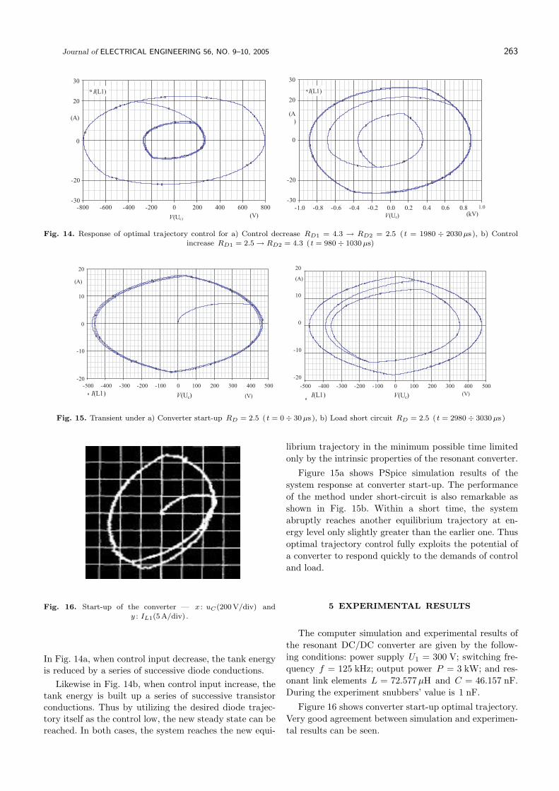
As noted in [1,9], the maximum rate at which the tankenergy can change in half a cycle is limited. Thus thesystem takes more than a half-cycle to reach the targettrajectory. Figure 14 shows the PSpice simulation resultsof the system response to large changes in control input.
Journal of ELECTRICAL ENGINEERING 56, NO. 9–10, 2005 263
Fig. 14. Response of optimal trajectory control for a) Control decrease RD1 = 4.3 → RD2 = 2.5 ( t = 1980 ÷ 2030 µs ), b) Controlincrease RD1 = 2.5 → RD2 = 4.3 ( t = 980 ÷ 1030 µs)
Fig. 15. Transient under a) Converter start-up RD = 2.5 ( t = 0 ÷ 30 µs ), b) Load short circuit RD = 2.5 ( t = 2980 ÷ 3030 µs )
Fig. 16. Start-up of the converter — x : uC(200 V/div) andy : IL1(5 A/div) .
In Fig. 14a, when control input decrease, the tank energyis reduced by a series of successive diode conductions.
Likewise in Fig. 14b, when control input increase, thetank energy is built up a series of successive transistorconductions. Thus by utilizing the desired diode trajec-tory itself as the control low, the new steady state can bereached. In both cases, the system reaches the new equi-
librium trajectory in the minimum possible time limited
only by the intrinsic properties of the resonant converter.
Figure 15a shows PSpice simulation results of the
system response at converter start-up. The performance
of the method under short-circuit is also remarkable as
shown in Fig. 15b. Within a short time, the system
abruptly reaches another equilibrium trajectory at en-
ergy level only slightly greater than the earlier one. Thus
optimal trajectory control fully exploits the potential of
a converter to respond quickly to the demands of control
and load.
5 EXPERIMENTAL RESULTS
The computer simulation and experimental results of
the resonant DC/DC converter are given by the follow-
ing conditions: power supply U1 = 300 V; switching fre-
quency f = 125 kHz; output power P = 3 kW; and res-
onant link elements L = 72.577µH and C = 46.157 nF.
During the experiment snubbers’ value is 1 nF.
Figure 16 shows converter start-up optimal trajectory.
Very good agreement between simulation and experimen-
tal results can be seen.

264 N. Bankov — T. Grigorova: LOAD CHARACTERISTICS AND CONTROL SYSTEM BEHAVIOURAL MODELLING UNDER . . .
4 CONCLUSIONS
In this paper we obtained steady-state equations inoptimal trajectory control, described DC/DC resonantconverter operation above the resonant frequency as afunction of the diode trajectory radius and correspondingnormalized load characteristics. They allow evaluatingthe behaviour of the considered converter when the loadis changed strongly during the operation process. Thecontrol system is described using ABM feature providedin OrCad PSpice.
The resonant tank energy is fully controlled with thetank energy, current and voltage, all staying well withinbounds under all circumstances, including a short circuitacross the converter output. The control automaticallyselects the optimum sequence of device condition underdynamic conditions. Very good agreement between simu-lation and experimental results can be seen.
The converters operated under this control techniqueare more suitable for electric arc welding devices, X-raydevices, lasers power supply etc, where for the supplysource, characteristics of the current source are required.
References
[1] ORUGANTI, R.—LEE, F. C. : Resonant Power Processor:Part II — Methods of control,, Proc. IEEE-IAS’84 Ann. Meet.,
pp. 868–878 , 1984.
[2] CHERON, Y. : La commutation douce dans la conversion sta-
tique de l’energie electrique, Technique et Documentation —Lavoisier, 1989.
[3] SIVAKUMAR, S.—NATARAJAN, K.—SHARAF, A. M. : Op-
timal Trajectory Control of Series Resonant Converter usingModified Capacitor Voltage Control Technique, Proc. IEEE–
PESC’91 Ann. Meet., Cambridge-Boston, pp. 752–759, June
1991.
[4] NATARAJAN, K.—SIVAKUMAR, S. : Optimal TrajectoryControl of Constant Frequency Series Rsonant Converter, 24th
Annual IEEE Power Electronics Specialists Conference PESC
’93, pp. 215–221, June 1993.
[5] ROSSETTO, L. : A Simple Control Technique for Series Res-
onant Converter, IEEE Trans. on Power Electronics 11 No. 4
(July 1996), 554–560.
[6] KUTKUT, N. H.—LEE, C. Q.—BATARSEH, I. : A General-
ized Program for Extracting the Control Characteristics of Res-
onant Converters via the State-Plane Diagram, IEEE Trans. on
Power Electronics 13 No. 1 (January 1998), 58–66.
[7] SENDANYOYE, V.—AL HADDAD, K.—RAJAGOPALAN,
V. : Optimal Trajectory Control Strategy for Improved Dynamic
Response of Series Resonant Converter, Proc. IEEE-IAS’90 Ann.
Meet., Seattle, WA, pp. 1236–1242, (October 1990).
[8] OrCAD PSpice A/D User’s Guide, OrCAD Inc., USA, 1999.
[9] AL-HADDAD, K.—CHERON, Y.—FOCH, H.—RAJAGOPA-
LAN, V. : Static and Dynamic Analysis of a Series Resonant
Converter Operating above its Resonant Frequency, SATECH’86
Proceedings, Boston, pp. 55-68, 1986.
Received 30 May 2005
Nikolay Dimitrov Bankov was born in 1957 in Plovdiv,
Bulgaria. He received the MS degree in electrical engineering
from the Technical University Sofia in 1983. In 1998 he re-
ceived his PhD in electrical converters. He is Assoc. Prof. in
the University of Food Technologies, Department of Electron-
ics. His research interests are in the fields of applied electron-
ics, power electronics, control techniques and digital simula-
tion.
Tsvetana Grigorova Grigorova was born in 1968 in
Plovdiv, Bulgaria. She received the MS degree in electronics
and automation from the Technical University Sofia in 1991.
In 2000 she received her PhD in electrical converters. Since
1992 till now she has been Assist. Prof. in Technical Univer-
sity of Sofia, Branch Plovdiv, Department of Electronics. Her
current interests include the development of high-frequency
resonant converters and their control, behavioural modelling
using PSpice. Dr. Grigorova is a member of IEEE Power Elec-
tronics Society.

![COMPARISONOFHONEYBEEMATINGOPTIMIZATION …iris.elf.stuba.sk/JEEEC/data/pdf/3_113-01.pdf · 2013. 5. 22. · system stability enhancement through improved damping of power swings [12]](https://img.pdfslide.net/doc/110x75/603e07791beee513e52b6291/comparisonofhoneybeematingoptimization-iriselfstubaskjeeecdatapdf3113-01pdf.jpg)