Embed Size (px)
Citation preview

SUBCOURSE EDITIONSS0605 7
LOGIC CIRCUITS AND DEVICES
(DEVELOPMENT DATE: 30 SEPTEMBER 1987)

US ARMY RADIO/TELEVISION SYSTEMS SPECIALISTMOS 26T SKILL LEVEL 1 COURSE
AUTHORSHIP RESPONSIBILITY:SSG Rene L. Thomas560th Signal BattalionVI/Cal Training Information
Development DivisionLowry AFB, ColoradoAUTOVON: 926-2521COMMERCIAL: (303) 370-2521
LOGIC CIRCUITS AND DEVICES(Developmental Date: 30 September 1987)
SUBCOURSE NO: SS0605-7
US Army Signal Center and Fort GordonFort Gordon, Georgia
Five Credit Hours
General
The Logic Circuits and Devices subcourse requires a basic understanding of Boolean mathematics. Thissubcourse is designed to teach you knowledge and skills for performing tasks related to operation andoperator's maintenance of electronic equipment. Information is provided on all the gates and theiroperations. The operations go from the simplest (turning on a light switch) to the most complex array ofgates (satellite communications). The subcourse is presented in three lessons, each lesson correspondingto a terminal objective as indicated below.
Lesson 1: DESCRIBE THE ELECTRONIC PARAMETERS OF LOGIC
TASK: Describe and identify logic symbols and positive and negative logic.
CONDITIONS: Given the difference between positive and negative logics, and the use of symbols.
STANDARDS: Demonstrate competency of the task skills and knowledge by correctly responding to80 percent of the multiple-choice test questions covering the information given in this lesson.
Lesson 2: DESCRIBE LOGIC SYSTEMS
TASK: Describe and identify how logic gates are combined and the changes of their outputs.
i
CONDITIONS: Given information about logic gates, describe the difference of some systems and theiroutputs.
STANDARDS: Demonstrate competency of the task skills and knowledge by completing a series oftruth tables and by correctly responding to 80 percent of the multiple-choice test questions relating tologic systems.
Lesson 3: DESCRIBE BASIC LOGIC CIRCUITS
TASK: Identify the switches, diodes, transistorized gates, and circuit symbols found in schematics.
CONDITIONS: Given data relating to switches, diodes, transistorized gates, circuit symbols, andschematic diagrams.
STANDARDS: Demonstrate competency of the task skills and knowledge by correctly responding to80 percent of the multiple-choice test questions relating to switches, diodes, transistorized gates, andcircuit symbols found in schematic diagrams.
This subcourse is designed to give you a working knowledge of logics, but not to fix or repair equipmentwithout additional knowledge of electronics.
This subcourse supports the following MOS 26T tasks: (STP 11-26TI3-SM-TG, September 1985)
113-575-0021 Troubleshoot and Repair a Television Receiver113-575-0038 Troubleshoot and Repair Video Pulse Distribution Amplifier113-575-0040 Troubleshoot and Repair a Sync Generator113-575-0041 Troubleshoot and Repair a Character Generator113-575-0042 Troubleshoot a Reel-to-reel Audio Tape Recorder/Reproducer113-575-0043 Troubleshoot a Color Television (TV) Camera113-575-0044 Troubleshoot a 3/4-inch Video Cassette Recorder/Reproducer (VCR)113-575-0045 Troubleshoot a Television Transmitter113-575-0046 Troubleshoot a Television (TV) Video Switcher113-575-0049 Troubleshoot a Time Base Corrector113-575-2040 Perform Functional Check of a Color Television (TV) Film Chain Camera113-575-2041 Perform Functional Check of a Color Television (TV) Camera System113-575-2042 Perform Functional Check of a Color Television (TV) Studio Camera
Colorplexer113-575-2043 Perform Functional Check of a Color Television (TV) Studio Camera113-575-2044 Perform Functional Check of a Small Format Television (TV) Recording
System, Using a 3/4-inch Video Cassette Recorder/Reproducer (VCR)113-575-2045 Perform Functional Check of a Time Base Corrector (TBC)113-575-2047 Perform Functional Check of a Television (TV) Transmitter113-575-3029 Perform Daily Maintenance on a 3/4-inch Video Cassette
Recorder/Reproducer (VCR)
ii

113-575-3031 Perform a Complete Color Convergence of a Color Television (TV) Receiver113-575-3033 Perform Measurement of the Visual and Audio Transmitter Carrier Frequency113-575-3035 Perform Daily Maintenance of a Television (TV) Video Switcher113-575-3036 Perform Preventive Maintenance of a Character Generator113-575-4010 Replace a Color Picture Tube (CRT)113-575-4011 Replace Faulty Television (TV) Studio Camera Cable113-575-4012 Replace RF Transmission Lines Between Antenna and RF Modulators113-575-8017 Perform Alignment Check of a Wave Form Monitor
*** IMPORTANT NOTICE ***
THE PASSING SCORE FOR ALL ACCP MATERIAL IS NOW 70%.
PLEASE DISREGARD ALL REFERENCES TO THE 75% REQUIREMENT.
iii

TABLE OF CONTENTS
Section Page
TITLE PAGE......................................................................................................................... i
TABLE CONTENTS............................................................................................................. iv
INTRODUCTION TO LOGIC CIRCUITS AND DEVICES ............................................... vii
Lesson 1: DESCRIBE THE ELECTRONIC PARAMETERS OF LOGIC ......................... 1
Learning Event 1: Identify the Use of Positive and Negative Logic Circuits .......... 1
Learning Event 2: Describe Negative and Positive Logic Circuits .......................... 2
Learning Event 3: Identify State Indicator and Inverter Symbols ............................ 3
Learning Event 4: Identify the OR and the AND Symbol........................................ 5
Practice Exercise........................................................................................................ 9
Lesson 2: DESCRIBE LOGIC SYSTEMS .......................................................................... 11
Learning Event 1: Define a Logic System................................................................ 11
Learning Event 2: Identify an OR Gate and the Inverter Combination .................... 12
Learning Event 3: Identify an AND Gate and the Inverter Combination................. 13
Learning Event 4: Explain How Combinations of Gates Can Change Functions .... 14
Practice Exercise........................................................................................................ 16
Lesson 3: DESCRIBE BASIC LOGIC CIRCUITS.............................................................. 17
Learning Event 1: Identify a Two Switch as a Logic OR Gate ................................ 17
Learning Event 2: Identify a Two Switch as an AND Gate ..................................... 22
iv

Learning Event 3: Define a NOR or NAND Circuit................................................. 26
Learning Event 4: Compare a Negative and Positive Logic Circuit......................... 28
Practice Exercise........................................................................................................ 33
ANSWERS TO PRACTICE EXERCISES ........................................................................... 34
Whenever pronouns or other references denoting gender appear in this document, they are written torefer to either male or female unless otherwise noted.
v

INTRODUCTION TO LOGIC CIRCUITS AND DEVICES
1. The terms "logic" and "logically" probably cause you to think of common sense, expectedresults, and rational decisions. These definitions or synonyms are the same ones connected with theword logic when the term is used in electronics. The term "logic" in electronics describes operationsand symbols of operations that follow a predetermined set of rules.
2. Transistorized circuitry and integrated circuits (IC) are being used more and more in newequipment. Many of these circuits, especially those that function in a binary manner, are standardized.They belong to specific classes of circuits depending on their function. As a result, symbolic logic isnow used not only with computers but also with data processing equipment, communications equipment- in almost every area in the electronic field.
3. To more easily understand the logic diagrams of existing equipment, you must have a thoroughknowledge of binary logic. You should recognize the symbols when they are used, know the meaningof each symbol, and know the rules governing their functions.
4. This subcourse has the information you need to learn and apply the principles of symbolic logicto military equipment. It is based on military standards of symbolic logic. Of course, once you havelearned the rules of binary logic thoroughly, any symbol variations you encounter in nonmilitary or oldernonstandard logic will be very easy to understand. You will only have to recognize new symbols - thefunction of the circuits they represent and the binary rules they follow will remain the same.
vii

LESSON 1DESCRIBE THE ELECTRONIC PARAMETERS OF LOGIC
TASK
Describe and identify logic symbols and positive and negative logic.
CONDITIONS
Given the description of positive and negative logics, and the use of symbols.
STANDARDS
Demonstrate competency of the task skills and knowledge by correctly responding to 80 percent of themultiple-choice test questions covering the information given in this lesson.
REFERENCES
None
Learning Event 1:IDENTIFY THE USE OF POSITIVE AND NEGATIVE LOGIC CIRCUITS
1. Symbols are used to present basic binary circuits because the symbols are time savers. Eachlogic symbol represents an entire circuit. By using the symbols, large schematics of electronicequipment can be reduced to smaller prints called logic diagrams. You no longer have to trace a signalthrough a complicated schematic if a logic diagram is available. Logic diagrams are more concise andeasier to read and understand.
2. For example, suppose that after studying the circuit shown in Figure 1-1 you find that it has a setpattern of operation. Each time you press two buttons the circuit operates and the bell rings. Once youhave studied the schematic and learned how the circuit rings the bell, there is no need to trace throughthe entire schematic each time the two buttons are pressed. You know why the bell rings; now you needto know when it rings.
a. Replacing the entire schematic with one symbol, as shown in Figure 1-2, you can then say,"If you know the inputs, you can predict the output." Each time you see that symbol you will recognizeit as a bell-ringer circuit and, logically, closing two input switches will ring the bell.
1
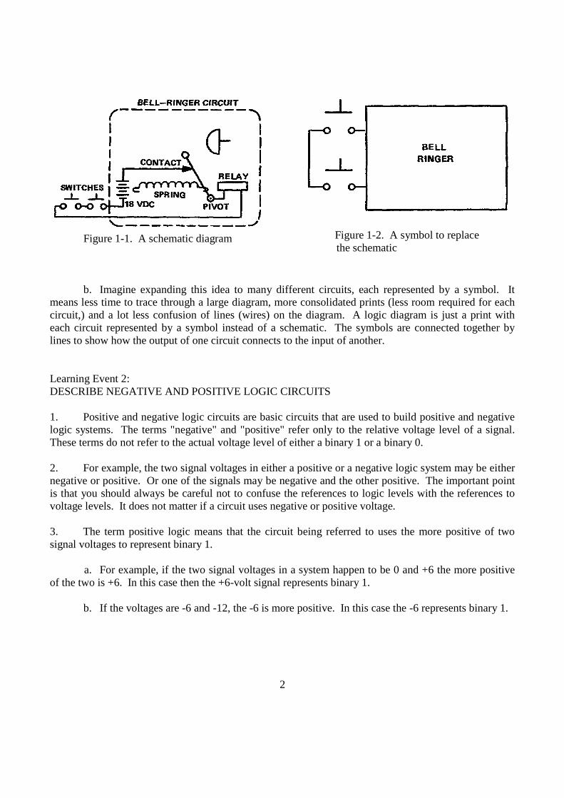
Figure 1-1. A schematic diagram Figure 1-2. A symbol to replacethe schematic
b. Imagine expanding this idea to many different circuits, each represented by a symbol. Itmeans less time to trace through a large diagram, more consolidated prints (less room required for eachcircuit,) and a lot less confusion of lines (wires) on the diagram. A logic diagram is just a print witheach circuit represented by a symbol instead of a schematic. The symbols are connected together bylines to show how the output of one circuit connects to the input of another.
Learning Event 2:DESCRIBE NEGATIVE AND POSITIVE LOGIC CIRCUITS
1. Positive and negative logic circuits are basic circuits that are used to build positive and negativelogic systems. The terms "negative" and "positive" refer only to the relative voltage level of a signal.These terms do not refer to the actual voltage level of either a binary 1 or a binary 0.
2. For example, the two signal voltages in either a positive or a negative logic system may be eithernegative or positive. Or one of the signals may be negative and the other positive. The important pointis that you should always be careful not to confuse the references to logic levels with the references tovoltage levels. It does not matter if a circuit uses negative or positive voltage.
3. The term positive logic means that the circuit being referred to uses the more positive of twosignal voltages to represent binary 1.
a. For example, if the two signal voltages in a system happen to be 0 and +6 the more positiveof the two is +6. In this case then the +6-volt signal represents binary 1.
b. If the voltages are -6 and -12, the -6 is more positive. In this case the -6 represents binary 1.
2
4. From the above examples, you can see that a system using positive logic may not even use apositive signal. A positive logic system is one that is classified or defined as a system in which the morepositive signal represents binary 1.
5. Since positive logic is defined as a system using the more positive of two signals to representbinary 1, it follows that negative logic must be a logic system that uses the more negative of two signalvoltages to represent binary 1.
6. The more negative of two voltages such as -6 and -12 is obviously the -12 and thus it representsbinary 1. In a system using +6 and +12 volts, the +6 is the more negative of the two and representsbinary 1.
Learning Event 3:IDENTIFY STATE INDICATOR AND INVERTER SYMBOLS
1. There are many different pairs of voltages in use and in some applications, such ascommunications, the levels are different in each piece of equipment. Therefore, common titles are usedto identify the two signals' conditions regardless of their actual levels. The system we will discuss hereis the most popular one and the least confusing. The two signal levels are simply called high and low,and are the same as 1 and 0.
a. The more positive of the two voltages is the high (H) and the more negative of the twovoltages is the low (L). This method has a great advantage in that it does not matter what the twovoltages are, one is always more positive than the other. Even if signal levels change from oneequipment to the other, the high and low concept can still be applied.
b. The method also allows us to discuss symbols and the circuit functions they represent,without regard to which voltage represents a binary 1 and which voltage represents a binary 0.
2. The military standard logic uses small circles called state indicators at the inputs and outputs ofthe logic symbols. The lines entering and leaving a symbol represent its input and output, the presenceor the absence of a circle on each line specifies what the active signal condition is for that connection.
a. The presence of a circle indicates that at that point in the circuit the relatively low (L) voltageis the active state of the signal. A circle on an input to a symbol means that a low is required to activateor "turn on" that circuit. A circle on the output means that the output is a low when the circuit isactivated or "turned on."
b. The absence of a circle indicates that at that point in the circuit the relatively high (H) voltageis the active state of the signal. The absence of a circle on an input to a symbol means that a high isrequired to activate or "turn-on" the circuit. Absence of a circle on the output means that the output ishigh when the circuit is activated or "turned on."
3

NOTE:
The circle is always a part of a symbol. It is never usedalone on a line to indicate signal levels or any other fact.
c. The state indicator allow us to predetermine the input signals required for any circuit and thecircuit's output level without regard to the function of the circuit. This fact will be correct regardless ofthe symbol. As we discuss each symbol, we will use the shape of the symbol to determine its circuitfunction, and the state indicators (circles) to determine the inputs required and the output produced.
Figure 1-3. An inverter symbol
3. When a binary circuit produces an output that is exactly the opposite of the input, it is called aninverter. The symbol for an inverter is shown in Figure 1-3. The inverter symbol is the only symbolthat will have one input and one output. All others will have two inputs or more. The inverter isconsidered a NOT gate.
4. The state indicator (circle) is shown as part of the inverter symbol on either its input or its output.It depends on whether the output is considered active when it is high or when it is low. Both versions ofthe symbol indicate that when the input is high the output is low and when the input is low the output ishigh. A comparison of the truth tables in Figure 1-3 proves this to be true.
5. An inverter performs the function of negation on signals and negates the Boolean expression ofthe input signals. Boolean algebra is a system of mathematical logic, using the function AND, NOT,and OR. In the Boolean system, AND is represented by multiplication, NOT by complementation, andOR by addition. So X and Y is written XY or X Y, NOT X is written X', and X OR Y is written X +Y. Boolean functions are used in the design of digital logic circuits. A simple term such as B at theinput to an inverter becomes B at the output. An expression such as A + B becomes A + B after aninverter. Simplifying this expression, (A + B) = (AB), we find that A + B becomes AB when it isinverted. This shows that an inverter negates the function, as well as the signal conditions in anexpression.
4

Learning Event 4:IDENTIFY THE OR AND THE AND SYMBOL
1. A circuit that performs an OR function is one that has at least two separate input connections andis activated or enabled by any one of them. The term "enable" is a common way to describe the actionof the signal that activates a gate. In binary logic, input signals don't usually force gates to produce anoutput; rather the input signals allow or enable a gate to produce an output. We usually think of inputsignals as either inhibiting a circuit or enabling it. Any signal that prevents a gate from producing itsactive output is called an inhibit signal; and, the signal that ultimately allows a gate to produce its activeoutput is called an enable signal.
a. The standard logic symbol for an OR circuit is shown in Figure 1-4. In the case of two inputs(A, B) to an OR gate, the circuit is activated or enabled by a specified input level to either input A orinput B. When the circuit is enabled it produces a specified output level. The Boolean expression forthe output is A + B.
Figure 1-4. OR circuit symbols
b. OR gates with more than two inputs connections are very common and we describe them inthe same way as the two input OR gate. The OR gate is activated if input A or B or C etc. is active. Ifmore than one input is active the result is the same, the circuit still produces an output. From thischaracteristic we determine that this symbol represents an inclusive OR, the conditions that cause anoutput include the condition where more than one input is active. Another way of describing the circuitoperation is "it produces an output if any one or more inputs is active."
5

2. Always remember that it's the shape of the signal that tells you the function and in this case thesymbols in Figure 1-4 represent OR gates. The presence or absence of state indicators (circles) onlyspecifies which voltage level (high or low) is required on each input and which level is produced.
a. Look at A of Figure 1-4. The absence of circles means the active signal is a high. We know,then, that the inputs require a high to enable the circuit because there are no circles on either of them.The absence of a circle on the output means that the gate produces a high output when it is active orenabled. From this we can say that the circuit requires a high in, to produce high out. But a high onwhich input? The symbol shape is "OR" so a high on input A or B or both causes a high out. Each ofthese conditions is shown in the truth table of Figure 3-17 on page 32.
b. The symbol in B, Figure 1-4, has circles on the input and output but the shape is still thesame so it's still an OR gate. A circle means a low is the active signal so this gate requires a low on A orB or both to produce a low output. The truth table in part B shows that the same four conditions as inpart A result in different output conditions. Obviously the circuits represented are both OR circuits.The difference is that one operates as an OR function of the relatively high signal, and the other as anOR function of the relatively low signal.
3. It's important that you realize we are discussing the function of circuits without looking at aschematic and knowing only how they respond to input signals. The circuits could be designed severaldifferent ways and still perform the same function. Thus, the inclusive OR symbol used here representsany and all inclusive OR circuits.
4. The exclusive OR is a variation of the OR symbol. The circuit it represents is still an OR circuitand performs an OR function; that's why the shape of the symbol is the same.
5. In A, Figure 1-5, for example, the gate requires a high on either input A or B just as the inclusiveOR does. The gate is "exclusive" in that it will not be enabled (produce an output) if both inputs arehigh. A complete description of exclusive OR operation is "either A or B but NOT BOTH."
a. Look at either of the truth tables in Figure 1-5. They show that the required output isproduced only when the inputs are not the same (not both high or both low.) The circuit represented bythe symbol in part A produces a high (no circle on the output) when it is enabled. Its truth tableindicates that it is enabled only when the inputs are not the same. When the inputs are both high or bothlow, the gate is inhibited and the output is low. The symbol in part B performs the same function butproduces a low when it is enabled. The Boolean expression for the output of this type of gate is writteneither AB + AB or A B.
6

Figure 1-5. Exclusive OR symbols
b. One use of the exclusive OR circuit is as a detection circuit in binary operations. Forexample, two signals that are always identical during normal operation can be compared by connectingthem to the inputs of an exclusive OR circuit. As long as they are the same (either both high or bothlow) the circuit will not be activated. However, if one of the signals fails or is incorrect, the gate isenabled and the resulting output indicates that an error has occurred.
6. A circuit that performs an AND function is one that produces an output only when all inputs areactive. Its operation can be described as producing an output either when A AND B are both active orwhen all inputs (A AND B AND C etc) are active.
7. The symbol for this type of gate is shown in Figure 1-6. As in the other symbols, its shapeindicates its function and state indicators tell you which level is considered the active signal. In A,Figure 1-6, the symbol represents a circuit that produces a high output if and only if all inputs are high.The one in part B produces a low output if and only if all inputs are low. This symbol (in either form)performs the Boolean function of AND; its output is expressed as A B or AB.
8. Since an AND gate requires that all inputs be active before it produces an active output, the lastinput signal to become active is called the enable signal. The other input (inputs, if there are more thantwo) is called the "prime" signal because it "primes" the gate or gets it ready for the last input signal toenable the gate. For AND gates that require high at the input, the first high input signal(s) primes thegate and the last high signal enables it.
7
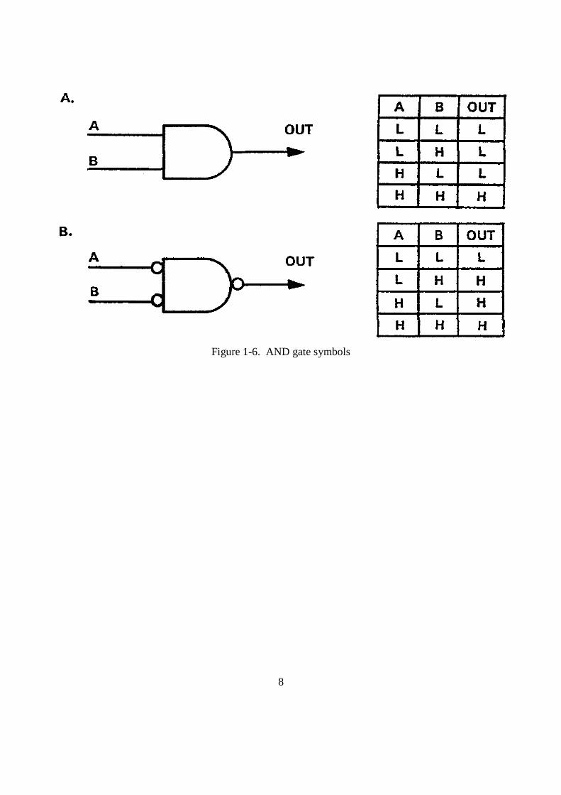
Figure 1-6. AND gate symbols
8

LESSON 1PRACTICE EXERCISE
1. What are the minimum inputs of an OR gate?
a. 0 or 1b. 1 or morec. 2 or mored. 3 or more
2. Any signal that prevents a gate from producing its active output is called?
a. Enable signalb. Positive signalc. Inhibit signald. Negative signal
3. Provided with two high inputs, which of the following gates will provide a high outputoperation?
a. Inverterb. Exclusive ORc. NORd. AND
4. What is the name of this symbol?
a. ANDb. ORc. NANDd. NOR
5. In a system using +6 and +12 which is the more negative?
a. +12 voltsb. Neither, they are both plusc. +6 voltsd. Add them together for plus 18
9

6. Which number is used to indicate a binary high?
a. 1b. 0c. 4d. 5
10
LESSON 2DESCRIBE LOGIC SYSTEMS
TASK
Describe and identify how logic gates are combined and the changes of their outputs.
CONDITIONS
Given information about logic gates, describe the differences of some systems and their outputs.
STANDARDS
Demonstrate competency of the task skills and knowledge by completing a series of truth tables and bycorrectly responding to 80 percent of the multiple-choice test questions relating to logic systems.
REFERENCES
None
Learning Event 1:DEFINE A LOGIC SYSTEM
1. The term "system" is used two different ways in binary logic. Logic system is used to mean anentire piece of equipment and groups of equipment that work together. It is also used to meancombinations of the basic symbols into groups that each perform a complete function.
2. When the term logic system is used in connection with equipment, it refers to the voltages thatare used as signal levels and indicates which voltage represents a binary 1. A negative logic system usesnegative logic, and a positive logic system uses positive logic.
3. Systems as discussed in this portion are simple combinations of the basic symbols into groups.By this definition, a group of gates that performs addition is a system; a group of gates that monitorsseveral signals and initiates an alarm if any signal fails is also a system.
11

Learning Event 2:IDENTIFY AN OR GATE AND THE INVERTER COMBINATION
1. Adding an inverter to the output of an OR gate is a widely used technique for varying the basicfunctions of OR and NOT. The OR-inverter combination is so useful that it has been given a name of itsown -- NOR gate. The OR gate, Figure 2-1, performs an OR function of the input signals and theinverter negates or "nots" the results. Hence, the name NOR (NOT OR). On a separate paper, completethe truth table in Figure 2-1 for the output of the inverter. Compare your results with Figure 3-17.
Figure 2-1. OR gate and inverter
2. A single circuit, and a single symbol to represent it, will also perform a NOR function: thesymbol is shown in Figure 2-2. Compare the Boolean expression at the output of the gate with theoutput expression in Figure 2-1; they are identical and the function is also identical.
3. According to the rules for state indicators, the gate in Figure 2-2 produces a low if any input is ahigh. Thus, to obtain a high output both inputs must be low; it produces a high out when neither A or Bis a high.
Figure 2-2. NOR gate symbol and truth table
4. Compare the truth table for the NOR gate in Figure 2-2 with the truth table you completed forFigure 2-1. They are the same which proves the symbols represent circuits that perform the samefunction. Do not, however, associate the circle on the output of the NOR gate with an independentinverter. The circle does not represent an inverter, it is only a state indicator. The NOR circuit invertsthe signal. It is not an OR gate followed by an inverter.
12

Learning Event 3:IDENTIFY AN AND GATE AND THE INVERTER COMBINATION
1. Connecting an inverter to the output of an AND gate, Figure 2-3, produces another function thatis very useful. The function is NOT AND, commonly called NAND. The function is NOT ANDbecause the AND gate performs and AND function of the input signals, then the inverter negates or"nots" the result. On a separate paper, complete the truth table in Figure 2-3 for the output of theinverter. Compare your result with Figure 2-2.
Figure 2-3. AND gate and inverter
2. The NAND function is so often used in equipment that, like the NOR gate, it has its own symbol:an AND gate symbol with a state indicator circle on the output and no indicators on the inputs as inFigure 2-4. But, because the function is the opposite of AND, it is called NOT AND. Compare the truthtable in Figure 2-4 with the one you completed in Figure 2-3; they should be identical. Thus, with theproper use of the state indicators, we have a single symbol to represent the inverter AND function. Acomplete description of the operational characteristics of the gate is: all highs in, a low out; and low in,a high out. Another way of stating the NAND function is that the circuit produces a high output if theinputs are NOT ANDed (not both high).
Figure 2-4. NAND gate symbol and truth table
13

Learning Event 4:EXPLAIN HOW COMBINATIONS OF GATES CAN CHANGE FUNCTIONS
1. Logic systems can be designed many different ways to produce a specific result. The circuitarrangement selected usually depends on the equipment designer. There is seldom a "best" way ofdesigning any binary system. Your job as a technician is to analyze and understand systems that alreadyexist, not to design systems. Very often, however, you will find that a careful analysis of a system orpartial system is the only way to prove its true operation.
2. Look at the system in Figure 2-5 for an example. At first glance it appears to perform an ORfunction of several inverted signals. If however, you use Boolean algebra, the system can be simplifiedand proved to be performing an entirely different function. Simplify the final expression and whatremains? A 3-input AND function of ABC. The function is not at all what it first seems to be; thefunction, at least for the output we are considering, represents an ANDing of the inputs.
Figure 2-5. A small system
3. A truth table confirms our analysis of the function. The only input combination that enables thecircuit to produce a high output is when A, B, and C are all true (high). Trace each combination listed inthe truth table through the gates to be sure you understand the results.
4. Normally, this circuit would not have been designed this way if only the ABC output was to beused; a single AND circuit would have been used instead. However, peculiar arrangements of basiccircuits such as this one often occur within large logic diagrams, usually because other combinations ofthe same input signals are required to satisfy other gates.
14

a. We could, for example, have an output tapped off gate 4 to use only the B + C functionsomewhere else. And perhaps the individual outputs of inverter 1, 2, or 3 are needed for driving othergates. A single AND gate would not provide these various output combinations.
b. Using Boolean algebra for labeling and simplifying will often enable you to clarify largesections of circuits when you study logic diagrams just as we simplified this small one.
15

LESSON 2PRACTICE EXERCISE
1. What is it called when single combinations of basic symbols are grouped together?
a. Logic systemb. Logic gatesc. Logic diagramd. Logic group
2. When an inverter is attached to an OR gate, what is the circuit called?
a. NANDb. NORc. OR-exclusived. Inverter
3. When two highs are applied to the input of an NOR gate, what is the output?
a. Lowb. Highc. Both A and Bd. Neither A or B
4. Which two combinations make a NAND gate?
a. AND and ORb. AND and Inverterc. AND and NORd. AND and Exclusive OR
5. What is one advantage of using Boolean algebra for labeling circuits?
a. There is no advantageb. It makes logic study easierc. It clarifies large sections of circuitsd. It allows the use of a slide rule in computations
16

LESSON 3DESCRIBE BASIC LOGIC CIRCUITS
TASK
Identify the switches, diodes, transistorized gates, and circuit symbols found in schematics.
CONDITIONS
Given data relating to switches, diodes, transistorized gates, circuit symbols, and schematic diagrams.
STANDARDS
Demonstrate competency of the task skills and knowledge by correctly responding to 80 percent of themultiple-choice test questions relating to switches, diodes, transistorized gates, and circuit symbolsfound in schematic diagrams.
REFERENCES
None
Learning Event 1:IDENTIFY A TWO SWITCH AS A LOGIC OR GATE
1. There are many circuits that perform the function of an OR gate. One of the simplest is a circuitwith two parallel switches and a lamp, Figure 3-1. The circuit is an OR gate because of the switcharrangement in the voltage supply to the lamp. If either switch A or B is closed, the lamp will light.Either A or B will connect +6 volts to the lamp and, since the other side is grounded, current will flow,lighting the lamp.
Figure 3-1. Two switches as an OR gate
17

a. Considering the light from the lamp as the output, let's relate the whole circuit to eitherpositive logic or negative logic OR gate. We've already determined that it follows the rules of an ORgate but how can we say that it represents one type of logic or another? Look at the voltage input andconsider the circuit operation again, first as a positive logic.
b. When both switches are open there is no voltage or 0 volts connected to the lamp and there isno output-light. The two operating voltages then are +6 and 0 volts and, since positive logic requiresthat the more positive voltage is the binary 1 or active signal, this circuit operates as positive logicbecause we have a positive output (light) when we have a positive input.
2. By changing the operating voltage to the switches, we can easily show the same circuit as anegative logic OR gate. When either switch (or both) is closed, the negative voltage lights the lamp.Since the more negative voltage produces an output, the circuit follows the rules of a negative OR gate:any one or more low inputs produces an output.
3. There is one other fact about the OR symbol that we should relate to the schematic. An OR gatecan have any number of input connections and still follow the rule that any one (or more) active inputproduces an output.
4. Look at Figure 3-1 again and imagine more switches connected in parallel with A and B. Closeany one switch and the lamp still lights. It's still an OR gate no matter how many switches areconnected in parallel.
5. A functional circuit (diode or gate) that is used in many applications can be almost as simple asthe circuit in paragraph 1. Figure 3-2A shows a simple circuit that functions as a positive logic OR gateand Figure 3-2B shows a similar circuit that functions as a negative logic OR gate.
a. For A, Figure 3-2, let's say the operating voltages are +6 and 0 volts. When either A or B isconnected to +6 volts, the associated diode is forward biased. Current flows from ground through theresistor, through the diode to the voltage source (the input). Since almost all the resistance in the circuitis the resistor, it will drop all of the voltage. Therefore, the voltage at the output will be +6 volts, thesame as the input.
b. It might be easier to see if you imagine each diode as an automatic switch. When zero voltsis connected to both inputs, the switches are open and the voltage below the resistor (0 volts) is theoutput level. When +6 volts is applied to an input, the associated switch closes and the +6 volts isconnected straight through to the output.
6. Part B, Figure 3-2, shows a negative OR gate with 0 and -6 volts as the operating voltages. It isexactly the same as part A except for the position of the diodes and the input voltages. When one ormore inputs is low (-6), the diode(s) is forward biased and the output is low (-6). The six volts aredropped across resistor R1. When all inputs are high (binary 0) the output is high.
18

Figure 3-2. Diode OR gates
7. Thus far, we haven't used a circuit that is really complicated enough to warrant using a symbol toreplace the whole schematic. But now let's examine a complex OR circuit that might be used inelectronic equipment, the basic transistorized OR gate.
8. Part A, Figure 3-2, shows a single positive OR circuit schematic. By itself it may look verycomplicated, but imagine having as many as 20 or more of these, plus other required circuits, on aschematic! The advantage of using a simple symbol to represent each becomes obvious. Each ORcircuit performs the same function on the inputs. Once we determine how one circuit works, we cansubstitute a small symbol for the entire circuit. The advantage: much smaller and less complicateddiagrams.
a. You're probably wondering why we bother using something so complicated to do the samething as the simple diode OR gate circuit. Well, there are other reasons but the primary reason is to getvoltage. Using the diode CR gate, we get only what we put into it, or even slightly less.
b. For example, if the input signal to the diode OR gate is +3.5 volts, the output will be +3.5volts or less. However, by using the transistorized OR gate of Figure 3-3, we can also get amplification.The same 3.5-volt input can produce a required 6-volt output. The advantage: a constant amplitudeoutput signal even with a weakened input signal.
9. Using 0 and -6 volts as the applied signal voltages, let's first check out the circuit operation withno active inputs: binary 0 (C volts) is applied to both inputs A and B.
a. There is no current through R1 and the base of Q1 is at ground (0 volts).
b. Q1 is an NPN transistor. With 0 volts on its base and emitter, Q1 is cut off (any currentunder these conditions is so negligible we'll call it cutoff). At cutoff, Q1 has no effect on the voltagedivider R2-R3.
19
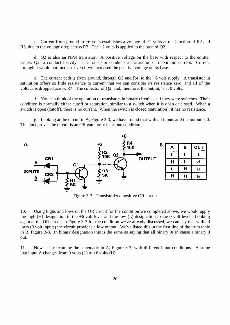
c. Current from ground to +6 volts establishes a voltage of +2 volts at the junction of R2 andR3, due to the voltage drop across R3. The +2 volts is applied to the base of Q2.
d. Q2 is also an NPN transistor. A positive voltage on the base with respect to the emittercauses Q2 to conduct heavily. The transistor conducts at saturation or maximum current. Currentthrough it would not increase even if we increased the positive voltage on its base.
e. The current path is from ground, through Q2 and R4, to the +6 volt supply. A transistor insaturation offers so little resistance to current that we can consider its resistance zero, and all of thevoltage is dropped across R4. The collector of Q2, and, therefore, the output, is at 0 volts.
f. You can think of the operation of transistors in binary circuits as if they were switches. Theircondition is normally either cutoff or saturation, similar to a switch when it is open or closed. When aswitch is open (cutoff), there is no current. When the switch is closed (saturation), it has no resistance.
g. Looking at the circuit in A, Figure 3-3, we have found that with all inputs at 0 the output is 0.This fact proves the circuit is an OR gate for at least one condition.
Figure 3-3. Transistorized positive OR circuit
10. Using highs and lows on the OR circuit for the condition we completed above, we would applythe high (H) designation to the +6 volt level and the low (L) designation to the 0 volt level. Lookingagain at the OR circuit in Figure 3-3 for the condition we've already discussed, we can say that with alllows (0 volt inputs) the circuit provides a low output. We've listed this in the first line of the truth tablein B, Figure 3-3. In binary designation this is the same as saying that all binary 0s in cause a binary 0out.
11. Now let's reexamine the schematic in A, Figure 3-3, with different input conditions. Assumethat input A changes from 0 volts (L) to +6 volts (H).
20

a. When the signal at input A changes to +6 volts (H), diode CR1 is forward biased and +6volts is developed across R1. The +6 volts at the top of R1 is felt at the base of Q1 and the forward biason the base-emitter function drives the transistor not only into conduction but also into saturation.
b. In saturation, the collector of Q1 drops to 0 volts (L) and this changes the R2-R3 voltagedivider. Q1 is in parallel with R3 and, in saturation, the low resistance of Q1 practically shorts out R3.It's like closing a switch that applies ground to the junction of R2 and R3. The current path is fromground, through the switch (Q1), and through R2 to the positive supply; R3 is bypassed.
c. The low at the R2-R3 function is applied to the base of Q2. With 0 volts on its base, Q2stops conducting. When current in Q2 stops, its collector voltage rises to the level of the supply voltage(+6).
d. The high at the collector also appears at the output. Thus, with a high on input A, the outputof the circuit is a high. This fact is shown in line 2 of the truth table. The OR gate proves correct with asecond condition: one active input (H) causes an output (H). Expressed in binary, this is stated as a 1 incauses a 1 out.
e. Assume now that input A returns it to low and input B rises to a high. What will happen?
(1) A high on input B forward biases CR 2 and the high is applied to the base of Q1. Exceptfor the diode used, the same action occurs as when input A received a high -; a high is applied to thebase of Q1.
(2) From this point on, the operation is the same as before. Q1 goes into saturation andapplies 0 volts to Q2. Q2 cuts off and the output is a high. Again a high in causes a high out. The thirdline of the truth table shows this condition. In general, any high (binary 1) into an OR gate causes a high(binary 1) out.
12. We have only one condition left to check through the schematic. What happens to the circuit ifmore than one input is a high? If the rules for OR gates hold true, the output should still be a high asindicated in line 4 of the truth table.
a. Having inputs A and B at +6 volts means that both CR1 and CR2 are forward biased.Resistor R1 still drops 6 volts and the +6 volts at the top of R1 biases Q1 into conduction.
b. From here on its operation is the same. Saturation of Q1 drops its collector voltage to 0 andthis drives Q2 into cutoff.
c. With Q2 cut off, the output is a high and the fourth condition completes the proof of the ORgate rule. We can now say that "any one or more high inputs causes a high output," or, "any 1 in causesa 1 out."
21

d. Since we've completely determined how the circuit works, we can replace it with a symbol.In Figure 3-4 for example, we can predict the output resulting from any given input combinationbecause we know how the circuit works.
13. On a separate piece of paper, complete the fourth column of the truth table as a final check toassure yourself that you understand the OR gate. Remember that in positive logic each high is a binary1 and each low is a binary 0. If you have any difficulty, refer back to the schematic in Figure 3-3 andimagine a third diode in parallel with the other two. The third diode provides the third input connectionrepresented by input C, Figure 3-4. The correct solution is shown on Figure 3-17.
Figure 3-4. Positive OR gate and truth table
14. A transistorized negative logic OR gate is similar to the circuit in Figure 3-3 but is designed tofollow the rules of negative logic. The difference compares to the difference between negative andpositive logic diode circuits.
Learning Event 2:IDENTIFY A TWO SWITCH AS AN AND GATE
1. A mechanical equivalent of an AND circuit can be shown just as easily as the first OR circuit wediscussed. All we need is two switches and a light bulb. This time, however, we connect the switches inseries instead of in parallel, as in Figure 3-5.
a. Once again we'll consider the light from the bulb as the output. When we explain how tolight the lamp, we will have stated the definition of an AND gate.
22

Figure 3-5. Two switch as an AND gate
b. Only if switch A AND switch B are closed is there an output - light.
c. Only with both switches closed will there be current from ground, through the bulb, to thevoltage source.
2. If we call the switches "inputs" and consider them "on" when they are closed, then the circuitfollows the rules we use to identify AND gates. If all the inputs are on, then the output is on, but if anyinput is off, then the output is off. Restated in logic circuit terminology: all is (highs) in, cause a 1(high) out. With -6 volts instead of +6 the circuit is a negative logic AND gate: all 1s (lows) in cause a1 (low) out.
3. A simple diode AND gate can be constructed with the same parts used for the OR gate - twodiodes and a resistor. For example, compare the circuits in Figure 3-6 with the circuits in Figure 3-2.They are the same with one exception; resistor R1 is connected to -6 or +6 volts instead of ground.
a. The following are the four possible conditions that can appear at the input to the diode ANDgate. We'll apply the conditions to a positive logic AND gate (B, Figure 3-6) with the voltage levels +6volts as a high, or binary 1; and, 0 voltage as a low, or binary 0.
Figure 3-6. Diode AND gate
23
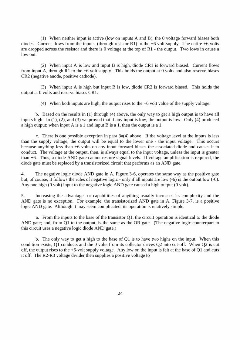
(1) When neither input is active (low on inputs A and B), the 0 voltage forward biases bothdiodes. Current flows from the inputs, (through resistor R1) to the +6 volt supply. The entire +6 voltsare dropped across the resistor and there is 0 voltage at the top of R1 - the output. Two lows in cause alow out.
(2) When input A is low and input B is high, diode CR1 is forward biased. Current flowsfrom input A, through R1 to the +6 volt supply. This holds the output at 0 volts and also reserve biasesCR2 (negative anode, positive cathode).
(3) When input A is high but input B is low, diode CR2 is forward biased. This holds theoutput at 0 volts and reserve biases CR1.
(4) When both inputs are high, the output rises to the +6 volt value of the supply voltage.
b. Based on the results in (1) through (4) above, the only way to get a high output is to have allinputs high. In (1), (2), and (3) we proved that if any input is low, the output is low. Only (4) produceda high output; when input A is a 1 and input B is a 1, then the output is a 1.
c. There is one possible exception in para 3a(4) above. If the voltage level at the inputs is lessthan the supply voltage, the output will be equal to the lower one - the input voltage. This occursbecause anything less than +6 volts on any input forward biases the associated diode and causes it toconduct. The voltage at the output, then, is always equal to the input voltage, unless the input is greaterthan +6. Thus, a diode AND gate cannot restore signal levels. If voltage amplification is required, thediode gate must be replaced by a transistorized circuit that performs as an AND gate.
4. The negative logic diode AND gate in A, Figure 3-6, operates the same way as the positive gatebut, of course, it follows the rules of negative logic - only if all inputs are low (-6) is the output low (-6).Any one high (0 volt) input to the negative logic AND gate caused a high output (0 volt).
5. Increasing the advantages or capabilities of anything usually increases its complexity and theAND gate is no exception. For example, the transistorized AND gate in A, Figure 3-7, is a positivelogic AND gate. Although it may seem complicated, its operation is relatively simple.
a. From the inputs to the base of the transistor Q1, the circuit operation is identical to the diodeAND gate; and, from Q1 to the output, is the same as the OR gate. (The negative logic counterpart tothis circuit uses a negative logic diode AND gate.)
b. The only way to get a high to the base of Q1 is to have two highs on the input. When thiscondition exists, Q1 conducts and the 0 volts from its collector drives Q2 into cut-off. When Q2 is cutoff, the output rises to the +6-volt supply voltage. Any low on the input is felt at the base of Q1 and cutsit off. The R2-R3 voltage divider then supplies a positive voltage to
24

the base of Q2 which drives it into conduction and holds the output low. Check each of the conditionsthrough the circuit to see if they agree with the truth table results (B, Figure 3-7).
Figure 3-7. Transistorized positive AND circuit
c. Any incoming positive signals that are lower than the operating level of the high (+6 volts inthis case) will be restored to full amplitude by the circuit. For example, if two +4-volt signals areapplied to the inputs in A, Figure 3-6, the high output will be +6 volts.
d. We can replace the entire schematic for this AND circuit with a symbol and still determineits output for any input condition. Look at the positive logic AND gate symbol in A, Figure 3-8. Now,follow the rules of an AND gate and complete the truth table in B, Figure 3-8. If you have anydifficulty, refer to the schematic in Figure 3-7. When you complete the truth table, check your resultswith the answer on Figure 3-17.
Figure 3-8. Positive AND gate and truth table
25

Learning Event 3:DEFINE A NOR OR NAND CIRCUIT
1. Two switches and a lamp can be arranged as shown in Figure 3-9 to represent the NOR function.If neither A nor B is closed (on) there is current through the lamp and light as the output. However, ifeither or both of the switches is closed (on) the output will be off. A closed switch provides a path oflower resistance than the lamp, so the current flows around the lamp. For this arrangement, there wouldhave to be a resistor between the power supply and the input point (labeled +6) to prevent a short toground when a switch is closed.
Figure 3-9. Two switches as a NOR gate
2. The transistorized NOR circuit shown in A, Figure 3-10, is less complicated than either thetransistorized AND or OR gate. Only one transistor is required for the NOR circuit. We don't need twotransistors because a NOR is just an OR with an inverter (NOT OR). The diodes (CR1, CR2) andresistor form a simple OR gate and Q1 is the inverter-amplifier.
a. When either input is a high, or both are high, the associated diode(s) is forward biased andthe positive potential is coupled to the base of Q1. Q1 conducts and the output is a low. The threepossible conditions of high inputs are lines 2, 3, and 4 of the truth table in B, Figure 3-10. Only whenthe inputs are both lows will the circuit provide a high output (line 1 of the truth table). A low on inputA and a low on input B reverse biases both diodes and a low is established on the base of Q1. A lowcauses Q1 to cut off and the output is a high. The binary expression for this circuit would be: a 1 outputif neither A NOR B is 1.
b. Notice that we get amplification or signal restoration from the NOR gate. For example, if thebinary 1 inputs to this circuit have degenerated to +3 volts, the output will be corrected to +6 volts.(You can see now that the transistor Q2 in the OR circuit schematic (fig 3-3) is needed only to reinvertthe output of Q1. Without it, the circuit is a NOR gate.)
26

Figure 3-10. Transistorized positive NOR circuit
3. A NAND gate output is high when any one or more inputs are low or NOT ANDed. When allinputs are on, the NAND gate output is off. Charging this to voltage levels and considering onlypositive logic, we can say that a NAND gate output is high (binary 1) when any input is low (binary 0).Also, when all inputs are high the output is low.
4. The switches and lamp circuit can be arranged as shown in Figure 3-11 so that it follows therules below. Here again, it is assumed that there is a resistor between the +6 VDC input and the powersupply that would prevent a short when the switches are all closed.
a. As long as one or more switches is open (low), there is current through the lamp and there isan output.
b. When both switches are closed (high) current flows around the lamp and there is no output.
Figure 3-11. Two switches as a NAND gate
5. Part A, Figure 3-12, is a typical positive logic NAND circuit. It consists of a diode AND gate(CR1, CR2, R1) and a transistor (Q1) to invert the signal. The output is high when any of the inputs arelow. These conditions are listed in the first three lines of the truth table (B, Figure 3-12).
27

Figure 3-12. Transistorized positive NAND circuit
a. The low on an input causes the associated diode to be forward biased because the diodes areconnected with their cathodes toward the input. The diode conducts and the low is coupled to the baseof Q1, cutting it off. This allows the output to rise to a high. Any low into this circuit causes a high out.
b. When all inputs are high, no input diode conducts. The positive supply voltage on R1 biasesQ1 in conduction, causing a low output. This is shown in line 4 of the truth table. The schematic thenfollows the rules of a NAND gate. As long as the inputs are NOT ANDed, the output is high.
Learning Event 4:COMPARE A NEGATIVE AND POSITIVE LOGIC CIRCUIT
1. While reading the preceding paragraphs, you may have sensed that there was something familiarabout some of the circuits and truth tables. If you did, the feeling was justified, there are someredundancies.
a. A circuit that performs a particular function in positive logic can be the same as a circuitperforming a different function in negative logic. In fact, they can be identical. And yet, they arerepresented by different symbols because the symbol only explains the circuit's function in somesituation. Put the circuit in a different function and it would be represented by a different symbol. Thesymbol, after all, only tells you what the circuit will do under different input conditions, not how thecircuit is physically constructed.
b. Now let's find out how this is possible. Look at the circuit in Figure 3-13 and be sure tonotice the title. On a separate paper complete the truth table (part B) and draw a symbol to represent thecircuit. Keep in mind that the symbol must accurately indicate the circuit's function for the type of logic(negative or positive) in use.
28

Figure 3-13. Negative logic circuit
Now look at Figure 3-14. Again, specifically notice the title and then on a separate papercomplete the truth table and draw a symbol to accurately represent it. Compare your results with theanswers in Figure 3-17.
Figure 3-14. Positive logic circuit
2. Figure 3-13 performs an AND function in negative logic, as indicated by the truth table, so it isrepresented by an AND symbol with circles at the inputs and output. Figure 3-14 performs an ORfunction in positive logic and is represented by an OR symbol with no circles on the inputs and output.But, comparing the two schematics we find that the circuits are identical. A negative AND gate, then,performs the same function as a positive OR gate. In most cases the schematics of the two gates are notidentical but it is possible. The important thing to note here is that logically, a negative AND and apositive OR are equivalent; they have the same truth table. Conversely, a positive AND and a negativeOR are also logically equivalent.
29

3. NAND and NOR gates can be compared the same way. A negative NAND is logicallyequivalent to a positive NOR as shown in Figure 3-15.
Figure 3-15. Negative NAND equals positive NOR
4. The truth table (B, Figure 3-15) is identical for the two symbols in A of the figure. Likewise, apositive NAND and a negative NOR are logically the same. The symbols represented in A (fig 3-15)may or may not be the same, (i.e., the symbol may have a line over it in one case, or without a line inanother), but the function is the same.
Figure 3-16. Positive NAND equals negative NOR
a. The only reason for using a different symbol is to present the most accurate picture of thecircuit function. In reality, NOR and NAND gates are not usually rigidly defined as we presented them.
b. The symbol used in a negative logic system may very well be a positive NOR or NAND.The symbol selected is the one that best describes the way the circuit is being used. This is especiallytrue in control logic where binary 1 or 0 is irrelevant and only highs and lows are important.
30

(1) Let's say we have a circuit from which we obtain a high when any input is low, and thehigh output is used to activate another circuit or light a lamp.
(2) We probably would select a NOR gate with circles on the input rather than the NANDsymbol with a circle at the output even though they perform the same function. The reason is that weusually select symbols that show the active output - in this case the high we need to activate a circuit orlight a lamp.
31
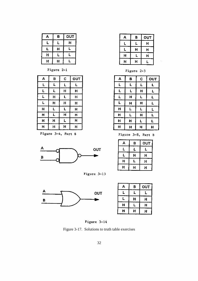
Figure 3-17. Solutions to truth table exercises
32

LESSON 3PRACTICE EXERCISE
1. How many input connections can an OR gate have?
a. Any numberb. 10c. 8d. 6
2. What is the name of the switch below (fig 3-1)?
a. OR gateb. NOR gatec. NAND gated. AND gate
3. When input A is low and input B is high, diode CR1 in Figure 3-6A is?
a. Reverse biasb. Forward biasc. Both a and bd. Neither a or b
4. On a three-input OR gate what inputs are needed to result in a low out (fig 3-4)?
a. All highsb. All lowsc. Two highsd. Two lows
5. On a three-input AND gate what inputs are needed to result in a high out (fig 3-8)?
a. All highsb. All lowsc. Two highsd. Two lows
33

ANSWERS TO PRACTICE EXERCISES
Lesson 1
1. c LE 4 para 1 pg 42. c LE 4 para 1 pg 53. d LE 4 para 7 pg 74. a LE 4 para 7 pg 85. c LE 2 para 6 pg 36. a LE 2 para 3a pg 3
LESSON 2
1. a LE 1 para 1 pg 112. b LE 2 para 1 pg 123. a LE 2 para 3 pg 124. b LE 3 para 1 pg 135. c LE 4 para 4b pg 15
LESSON 3
1. a LE 1 para 3 pg 182. a LE 1 para 1 pg 173. b LE 2 para 3(2) pg 244. b LE 1 para 13 fig 3-4 pg 225. a LE 2 para 5 fig 3-8 pg 25
34