Embed Size (px)
Citation preview
Logic Design Lab EEL3712l Experiment 3
P a g e 1 | 17
EXPERIMENT 3
Boolean Laws & Rules and
DeMorgan’s Theorem
OBJECTIVES:
Learn and verify Boolean laws and rules.
Learn and prove DeMorgan’s theorem
Use Xilinx simulation tools to test combinational circuits.
MATERIALS:
Xilinx Vivado software, student or professional edition V2018.2 or higher.
IBM or compatible computer with Pentium III or higher, 128 M-byte RAM or more, and 8
G-byte Or larger hard drive.
BASYS 3 Board.
DISCUSSION:
A Boolean equation derived directly from a truth table or from a problem statement usually is
not in the simplest form. To have an efficient equivalent logic circuit, the Boolean equation
representing the logic design must be in the simplest from. Boolean equations can be simplified
using Boolean algebra, DeMorgan’s theorem, or/and Karnaugh maps. In this experiment, we will
first present Boolean Laws and rules as well as DeMorgan’s theorem, and then verify them.

Logic Design Lab EEL3712l Experiment 3
P a g e 2 | 17
PROCEDURE:
Section I. Boolean Distributive Law
1. Open Xilinix Vivado.
2. In the Xilinx-Project Navigator window, Quick start, New Project.
Logic Design Lab EEL3712l Experiment 3
P a g e 3 | 17
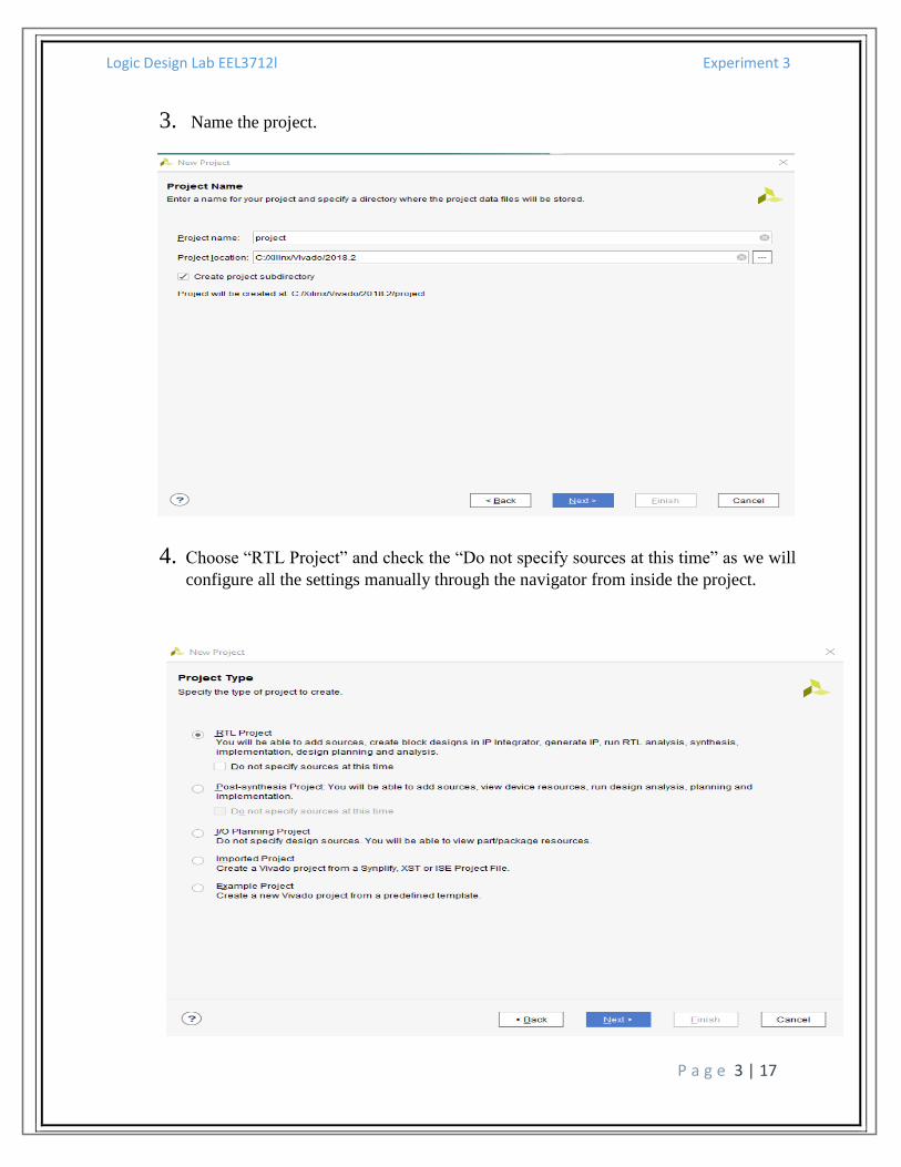
3. Name the project.
4. Choose “RTL Project” and check the “Do not specify sources at this time” as we will
configure all the settings manually through the navigator from inside the project.

Logic Design Lab EEL3712l Experiment 3
P a g e 4 | 17
5. Select New Source… and the New window appears. In the New window, choose
Schematic, type your file name (such as source_1) in the File Name editor box, click
on OK, and then click on the Next button.
Logic Design Lab EEL3712l Experiment 3
P a g e 5 | 17
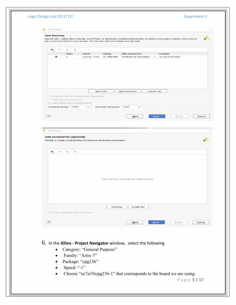
6. In the Xilinx - Project Navigator window, select the following
Category: “General Purpose”
Family: “Artix-7”
Package: “cpg236”
Speed: “-1”
Choose “xc7a35tcpg236-1” that corresponds to the board we are using.

Logic Design Lab EEL3712l Experiment 3
P a g e 6 | 17
Then Choose Finish.
Logic Design Lab EEL3712l Experiment 3
P a g e 7 | 17
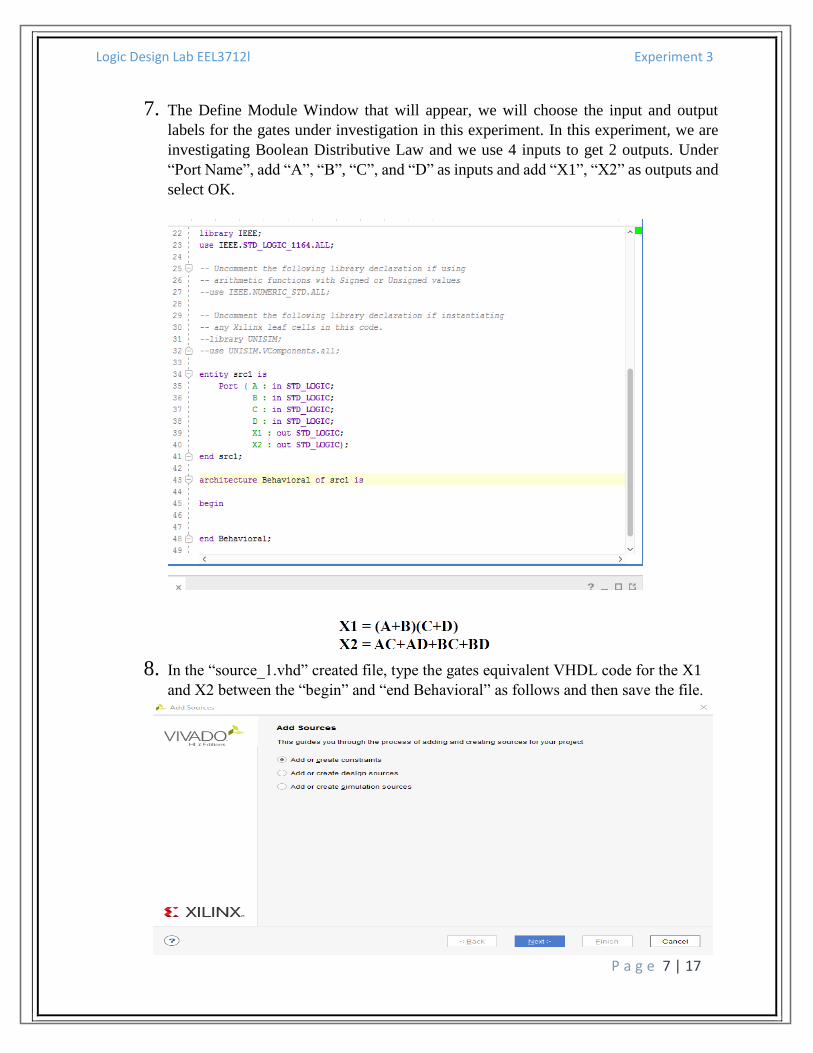
7. The Define Module Window that will appear, we will choose the input and output
labels for the gates under investigation in this experiment. In this experiment, we are
investigating Boolean Distributive Law and we use 4 inputs to get 2 outputs. Under
“Port Name”, add “A”, “B”, “C”, and “D” as inputs and add “X1”, “X2” as outputs and
select OK.
8. In the “source_1.vhd” created file, type the gates equivalent VHDL code for the X1
and X2 between the “begin” and “end Behavioral” as follows and then save the file.

Logic Design Lab EEL3712l Experiment 3
P a g e 8 | 17
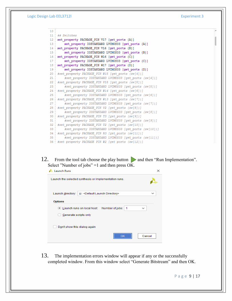
9. Next, we need to add to add a constraint file with the”.xdc” extension, as following:
Go to “Flow Navigator” and from “Project Manager” select “Add Sources” then “Add
or create constraints”. Next, choose “Create File” and enter the file name “lab_2” then
“OK” followed by “Finish”.
10. Then, we need to get a template xdc file that is going to be edited according to the
different experiments. Google “basys 3 xdc file” and choose the “xilinix” link that
appears (https://www.xilinx.com/support/documentation/university/Vivado-
Teaching/HDL-Design/2015x/Basys3/Supporting%20Material/Basys3_Master.xdc).
Copy the whole file and paste it into the “lab_2.xdc” that you have just created in the
last step. Then uncomment and edit the input Switches and the output LEDs as in the
next step.
11. Uncomment (by deleting the # sign) sw[0], sw[1], sw[3],….. led[0], led[1],…
lines. Note that each of them has two successive lines (Uncomment both of them). Do
the following replacements: sw[0] A, sw[1] B,……, led[0] X1, led[1]
X2 then save the file.
Logic Design Lab EEL3712l Experiment 3
P a g e 9 | 17
12. From the tool tab choose the play button and then “Run Implementation”.
Select ”Number of jobs” =1 and then press OK.
13. The implementation errors window will appear if any or the successfully
completed window. From this window select “Generate Bitstream” and then OK.

Logic Design Lab EEL3712l Experiment 3
P a g e 10 | 17
This will make the software generate “.bin” file to be used in programing the
hardware BAYAS 3.
14. The next window will appear in which choose “Open Hardware Manger”, connect
the Hardware Kit to the USB port and then press OK.

Logic Design Lab EEL3712l Experiment 3
P a g e 11 | 17
15. A green tab will appear in the top of the Vivado window, from which choose
“open target” to program the hardware.
16. From the window appears, select the “.bin” file from the Project you
create by browsing for the generated “.bit file” under the “.runs” folder and program
the board then press OK.
17. Test the program on your board by going through all the input combinations and
observing the two outputs. Fill the truth table.
Truth Table (1)
A B C D X1 X2
0 0 0 0
0 0 0 1
0 0 1 0
0 0 1 1
0 1 0 0
Symbol
Boolean Equation

Logic Design Lab EEL3712l Experiment 3
P a g e 12 | 17
0 1 0 1
0 1 1 0
0 1 1 1
1 0 0 0
1 0 0 1
1 0 1 0
1 0 1 1
1 1 0 0
1 1 0 1
1 1 1 0
1 1 1 1
18. Then you can use the simulation tools to verify the Boolean distributive law. For
simulation, we need to create a simulation source file as following:
19. “Flow Navigator” “Project Manager” “Add Sources” “Add or create
simulation sources” Name it “TB” (Test Bench) “VHDL” No need for
switches and leds assignments as we will not be working on board. “OK”.
20. In the “initialization” section write “A <= '0'; B <= '0'; C <= '0'; D <='0';”. In
the stimulus section, the following code (as in the figure) is written to simulate the
whole truth table:

Logic Design Lab EEL3712l Experiment 3
P a g e 13 | 17

Logic Design Lab EEL3712l Experiment 3
P a g e 14 | 17
Section II. Boolean Absorption Rule
The two shown below are called absorption rules.
You are asked to prove them using either your target board or simulation tools.
TIPS: You can combine the Section II and Section III together, draw them in only one project.
Logic Design Lab EEL3712l Experiment 3
P a g e 15 | 17
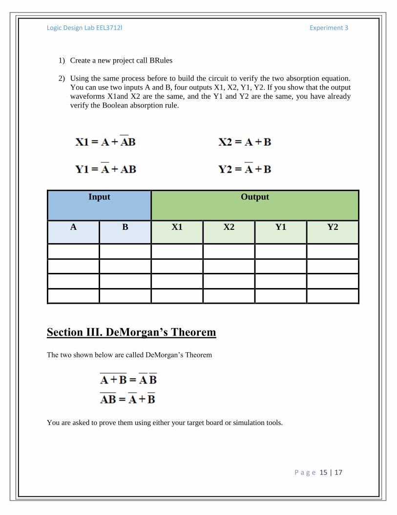
1) Create a new project call BRules
2) Using the same process before to build the circuit to verify the two absorption equation.
You can use two inputs A and B, four outputs X1, X2, Y1, Y2. If you show that the output
waveforms X1and X2 are the same, and the Y1 and Y2 are the same, you have already
verify the Boolean absorption rule.
Input Output
A B X1 X2 Y1 Y2
Section III. DeMorgan’s Theorem The two shown below are called DeMorgan’s Theorem
You are asked to prove them using either your target board or simulation tools.

Logic Design Lab EEL3712l Experiment 3
P a g e 16 | 17
1) Create a new project called Demorgan, build the circuit that enable you to prove the two
equations. You will need two inputs A and B, two pairs of outputs.
2) Fill the form
Input Output
A B X1 X2 Y1 Y2
Checked by____________________________ Date _____________________

Logic Design Lab EEL3712l Experiment 3
P a g e 17 | 17
QUESTIONS:
1) Draw the logic diagrams and list the truth tables for all the Boolean algebra rules except the
absorption rule.
2) Apply Boolean laws and rules and DeMorgan’s theorem to simplify the following Boolean
equations. Draw the simplified logic diagrams.