Embed Size (px)
Citation preview

Logic Design with MOSFETs
Dae Hyun Kim
EECS Washington State University

References
• John P. Uyemura, “Introduction to VLSI Circuits and Systems,” 2002. – Chapter 2
• Neil H. Weste and David M. Harris, “CMOS VLSI Design: A Circuits and Systems Perspective,” 2011. – Chapter 1

Goal
• Design logic gates using MOSFETs (NMOS and PMOS)

Signals and Wires
• Signals – 0 = 𝑉𝑉𝑆𝑆𝑆𝑆 = Ground = GND = Low = 0V – 1 = 𝑉𝑉𝐷𝐷𝐷𝐷 = Power = PWR = High = 5V, 3.3V, 1.5V, 1.2V, 1.0V, etc.
• Wires
𝑉𝑉𝐷𝐷𝐷𝐷
a
Wire 1
b Wire 2
No connection
a
a
Connection
a
a

Ideal Switches
• Switch
• Assert-high switch
• Assert-low switch
Control Control
𝑥𝑥 𝑦𝑦 𝑥𝑥 𝑦𝑦
Electrically short Electrically open
𝑨𝑨 = 𝟏𝟏
𝑥𝑥 𝑦𝑦 = 𝑥𝑥 𝑥𝑥 𝑦𝑦
𝑨𝑨 = 𝟎𝟎
Open (𝑦𝑦 is undefined) Closed (𝒚𝒚 = 𝒙𝒙)
𝑨𝑨 = 𝟏𝟏
𝑥𝑥 𝑦𝑦 = 𝑥𝑥 𝑥𝑥 𝑦𝑦
𝑨𝑨 = 𝟎𝟎
Open (𝑦𝑦 is undefined) Closed (𝒚𝒚 = 𝒙𝒙)
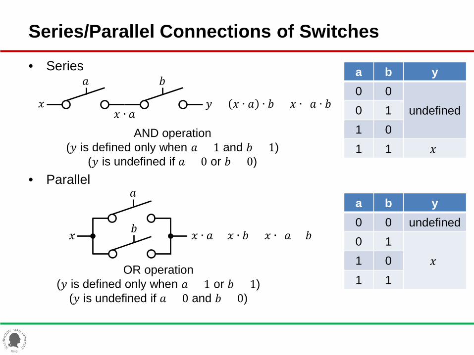
Series/Parallel Connections of Switches
• Series
• Parallel
𝑎𝑎 𝑏𝑏
𝑥𝑥 𝑥𝑥 ∙ 𝑎𝑎
𝑦𝑦 = 𝑥𝑥 ∙ 𝑎𝑎 ∙ 𝑏𝑏 = 𝑥𝑥 ∙ (𝑎𝑎 ∙ 𝑏𝑏)
AND operation (𝑦𝑦 is defined only when 𝑎𝑎 = 1 and 𝑏𝑏 = 1)
(𝑦𝑦 is undefined if 𝑎𝑎 = 0 or 𝑏𝑏 = 0)
𝑏𝑏
𝑎𝑎
𝑥𝑥 𝑥𝑥 ∙ 𝑎𝑎 + 𝑥𝑥 ∙ 𝑏𝑏 = 𝑥𝑥 ∙ (𝑎𝑎 + 𝑏𝑏)
OR operation (𝑦𝑦 is defined only when 𝑎𝑎 = 1 or 𝑏𝑏 = 1)
(𝑦𝑦 is undefined if 𝑎𝑎 = 0 and 𝑏𝑏 = 0)
a b y 0 0
undefined 0 1 1 0 1 1 𝑥𝑥
a b y 0 0 undefined 0 1
𝑥𝑥 1 0 1 1

Inverter Design with Switches
• Inverter – The output is defined both when 𝑎𝑎 = 0 and when 𝑎𝑎 = 1.
𝑎𝑎
𝑎𝑎
1
0
1 ∙ 𝑎𝑎�
0 ∙ 𝑎𝑎
𝑦𝑦 = 1 ∙ 𝑎𝑎� + 0 ∙ 𝑎𝑎 = 𝑎𝑎� a y 0 1 1 0

Inverter Design with Switches
• Two inverter designs
𝑎𝑎
𝑎𝑎
1
0
𝑦𝑦
𝑎𝑎�
𝑎𝑎�
0
1
𝑦𝑦 Why?

MOSFETs as Switches
• MOSFET: Metal-Oxide-Semiconductor Field-Effect Transistor – n-channel MOSFET = nFET = NMOS – p-channel MOSFET = pFET = PMOS – Complementary MOS: CMOS
• Symbols
nFET pFET
Gate
Source Drain Drain Source
Gate
= =
𝑉𝑉𝐺𝐺
𝑉𝑉𝑆𝑆 𝑉𝑉𝐷𝐷 𝑉𝑉𝐷𝐷 𝑉𝑉𝑆𝑆
𝑉𝑉𝐺𝐺
(𝑉𝑉𝐷𝐷 ≥ 𝑉𝑉𝑆𝑆) (𝑉𝑉𝑆𝑆 ≥ 𝑉𝑉𝐷𝐷)

MOSFETs as Switches
• Threshold voltage – nFET: 𝑉𝑉𝑇𝑇𝑛𝑛 > 0 – pFET: 𝑉𝑉𝑇𝑇𝑝𝑝 < 0
• nFET
– OFF: 𝑉𝑉𝐺𝐺𝑆𝑆𝑛𝑛 ≤ 𝑉𝑉𝑇𝑇𝑛𝑛 – ON: 𝑉𝑉𝐺𝐺𝑆𝑆𝑛𝑛 > 𝑉𝑉𝑇𝑇𝑛𝑛
• pFET
– OFF: 𝑉𝑉𝑆𝑆𝐺𝐺𝑝𝑝 ≤ |𝑉𝑉𝑇𝑇𝑝𝑝|
– ON: 𝑉𝑉𝑆𝑆𝐺𝐺𝑝𝑝 > |𝑉𝑉𝑇𝑇𝑝𝑝|
Gate
Source
Drain
Source
Drain
Gate
𝑉𝑉𝐴𝐴
𝑉𝑉𝐴𝐴
Logic translation 0
𝑉𝑉𝑇𝑇𝑛𝑛
𝑉𝑉𝐷𝐷𝐷𝐷
𝐴𝐴 = 0: Mn OFF
Mn
Mp
𝐴𝐴 = 1: Mn ON
𝑉𝑉𝐷𝐷𝐷𝐷 𝑉𝑉𝐴𝐴
Logic translation 0
𝑉𝑉𝐷𝐷𝐷𝐷 − |𝑉𝑉𝑇𝑇𝑝𝑝| 𝑉𝑉𝐷𝐷𝐷𝐷
𝐴𝐴 = 0: Mp ON
𝐴𝐴 = 1: Mp OFF
𝑉𝑉𝐴𝐴

MOSFETs as Switches • Example (PTM High-Performance 45nm High-K Metal Gate)
– 𝑉𝑉𝐷𝐷𝐷𝐷: 1.0V – 𝑉𝑉𝑇𝑇𝑛𝑛: 0.46893V – 𝑉𝑉𝑇𝑇𝑝𝑝: -0.49158V
• Example (PTM High-Performance 32nm High-K Metal Gate)
– 𝑉𝑉𝐷𝐷𝐷𝐷: 0.9V – 𝑉𝑉𝑇𝑇𝑛𝑛: 0.49396V – 𝑉𝑉𝑇𝑇𝑝𝑝: -0.49155V
• Example (PTM High-Performance 22nm High-K Metal Gate)
– 𝑉𝑉𝐷𝐷𝐷𝐷: 0.8V – 𝑉𝑉𝑇𝑇𝑛𝑛: 0.50308V – 𝑉𝑉𝑇𝑇𝑝𝑝: -0.4606V

Pass Characteristics
• nFET
• pFET
𝑉𝑉𝐺𝐺 = 𝑉𝑉𝐷𝐷𝐷𝐷
𝑉𝑉𝑆𝑆 = 𝑉𝑉𝑜𝑜𝑜𝑜𝑜𝑜
𝑉𝑉𝐷𝐷 = 𝑉𝑉𝑖𝑖𝑖𝑖 𝑽𝑽𝒊𝒊𝒊𝒊 ↑ 𝑽𝑽𝑮𝑮𝑮𝑮 ↓ 𝑽𝑽𝒐𝒐𝒐𝒐𝒐𝒐 ↑
0 𝑉𝑉𝐷𝐷𝐷𝐷 0
0.1 𝑉𝑉𝐷𝐷𝐷𝐷 - 0.1 0.1
... ... ...
𝑉𝑉𝐷𝐷𝐷𝐷 − 𝑉𝑉𝑇𝑇𝑛𝑛 𝑉𝑉𝑇𝑇𝑛𝑛 𝑉𝑉𝐷𝐷𝐷𝐷 − 𝑉𝑉𝑇𝑇𝑛𝑛
𝑉𝑉𝐷𝐷𝐷𝐷 𝑉𝑉𝑇𝑇𝑛𝑛 𝑉𝑉𝐷𝐷𝐷𝐷 − 𝑉𝑉𝑇𝑇𝑛𝑛
Logic 0 transfer: strong logic 0
Logic 1 transfer: weak logic 1
𝑉𝑉𝐺𝐺 = 0 𝑽𝑽𝒊𝒊𝒊𝒊 ↓ 𝑽𝑽𝑮𝑮𝑮𝑮 ↓ 𝑽𝑽𝒐𝒐𝒐𝒐𝒐𝒐 ↓ 𝑉𝑉𝐷𝐷𝐷𝐷 𝑉𝑉𝐷𝐷𝐷𝐷 𝑉𝑉𝐷𝐷𝐷𝐷
𝑉𝑉𝐷𝐷𝐷𝐷 − 𝜀𝜀 𝑉𝑉𝐷𝐷𝐷𝐷 − 𝜀𝜀 𝑉𝑉𝐷𝐷𝐷𝐷 − 𝜀𝜀
... ... ...
|𝑉𝑉𝑇𝑇𝑝𝑝| 𝑉𝑉𝑇𝑇𝑝𝑝 |𝑉𝑉𝑇𝑇𝑝𝑝|
0 0 |𝑉𝑉𝑇𝑇𝑝𝑝| Logic 0 transfer: weak logic 0
Logic 1 transfer: strong logic 1
𝑉𝑉𝑆𝑆 = 𝑉𝑉𝑖𝑖𝑖𝑖
𝑉𝑉𝐷𝐷 = 𝑉𝑉𝑜𝑜𝑜𝑜𝑜𝑜

Pass Characteristics
• SPICE simulation (45nm technology) – nFET
𝑉𝑉𝐷𝐷𝐷𝐷
𝑉𝑉𝑜𝑜𝑜𝑜𝑜𝑜
𝑉𝑉𝑖𝑖𝑖𝑖

Pass Characteristics
• SPICE simulation (45nm technology) – pFET
0
𝑉𝑉𝑜𝑜𝑜𝑜𝑜𝑜
𝑉𝑉𝑖𝑖𝑖𝑖

Pass Characteristics
• nFET – Strong logic 0 transfer – Weak logic 1 transfer
• pFET
– Strong logic 1 transfer – Weak logic 0 transfer
• CMOS
– Use pFETs to pass logic 1. – Use nFETs to pass logic 0.

Basic Logic Gates in CMOS
• Principles – Construct the nFET network using only nFETs and the pFET network
using only pFETs. – If the output is 1, the pFET network connects 𝑉𝑉𝐷𝐷𝐷𝐷 to the output and the
nFET network disconnects 𝑉𝑉𝑆𝑆𝑆𝑆 and the output. – If the output is 0, the nFET network connects 𝑉𝑉𝑆𝑆𝑆𝑆 to the output and the
pFET network disconnects 𝑉𝑉𝐷𝐷𝐷𝐷 and the output.
pFET network
𝑓𝑓 (output)
𝑉𝑉𝐷𝐷𝐷𝐷
𝑎𝑎, 𝑏𝑏, 𝑐𝑐, … (inputs)
nFET network

Basic Logic Gates in CMOS
• Inverter
𝑥𝑥 𝑓𝑓 = �̅�𝑥
0 𝑓𝑓 = 1 1 𝑓𝑓 = 0
off
off
𝑓𝑓 = �̅�𝑥 ∙ 1 + 𝑥𝑥 ∙ 0 = �̅�𝑥
# TRs: 2 nFET: 1 pFET: 1

Basic Logic Gates in CMOS
• SPICE simulation

Basic Logic Gates in CMOS
• Two-input NAND (NAND2)
𝑓𝑓 = 𝑎𝑎� ∙ 𝑏𝑏� ∙ 1 + 𝑎𝑎� ∙ 𝑏𝑏 ∙ 1 + 𝑎𝑎 ∙ 𝑏𝑏� ∙ 1 + 𝑎𝑎 ∙ 𝑏𝑏 ∙ 0 = 𝑎𝑎� + 𝑏𝑏� = 𝑎𝑎 ∙ 𝑏𝑏
𝑎𝑎 𝑓𝑓 = 𝑎𝑎 ∙ 𝑏𝑏
𝑏𝑏
0 𝑓𝑓 = 1
0
1 𝑓𝑓 = 0
1
off
off
0 𝑓𝑓 = 1
1
off
off
off off
# TRs: 4 nFETs: 2 pFETs: 2

Basic Logic Gates in CMOS
• SPICE simulation

Basic Logic Gates in CMOS
• Two-input NOR (NOR2)
𝑎𝑎 𝑓𝑓 = 𝑎𝑎 + 𝑏𝑏
𝑓𝑓 = 𝑎𝑎� ∙ 𝑏𝑏� ∙ 1 + 𝑎𝑎� ∙ 𝑏𝑏 ∙ 0 + 𝑎𝑎 ∙ 𝑏𝑏� ∙ 0 + 𝑎𝑎 ∙ 𝑏𝑏 ∙ 0 = 𝑎𝑎� ∙ 𝑏𝑏� = 𝑎𝑎 + 𝑏𝑏
𝑏𝑏
# TRs: 4 nFETs: 2 pFETs: 2
𝑎𝑎
𝑏𝑏
0 𝑓𝑓 = 1
0 0
0
off off
0
1 0
1
off
off 𝑓𝑓 = 0
1 𝑓𝑓 = 0
1 1
1
off
off

Basic Logic Gates in CMOS
• SPICE simulation

Complex Logic Gates in CMOS
• Example
• Using logic gates
• Using logic gates
• Using TRs
𝑓𝑓 = 𝑎𝑎 ∙ (𝑏𝑏 + 𝑐𝑐)
𝑏𝑏 𝑐𝑐
𝑎𝑎
𝑓𝑓 # TRs: 14 nFETs: 7 pFETs: 7
𝑏𝑏 𝑐𝑐
𝑎𝑎
𝑓𝑓 # TRs: 10 nFETs: 5 pFETs: 5
# TRs: 6 nFETs: 3 pFETs: 3
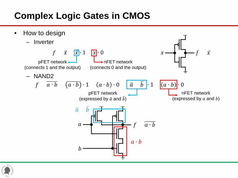
Complex Logic Gates in CMOS
• How to design – Inverter
– NAND2
𝑓𝑓 = �̅�𝑥 = �̅�𝑥 ∙ 1 + 𝑥𝑥 ∙ 0 𝑥𝑥 𝑓𝑓 = �̅�𝑥 nFET network
(connects 0 and the output) pFET network
(connects 1 and the output)
𝑓𝑓 = 𝑎𝑎 ∙ 𝑏𝑏 = 𝑎𝑎 ∙ 𝑏𝑏 ∙ 1 + 𝑎𝑎 ∙ 𝑏𝑏 ∙ 0 = (𝑎𝑎� + 𝑏𝑏�) ∙ 1 + 𝑎𝑎 ∙ 𝑏𝑏 ∙ 0 nFET network
(expressed by 𝑎𝑎 and 𝑏𝑏) pFET network
(expressed by 𝑎𝑎� and 𝑏𝑏�)
𝑎𝑎 𝑓𝑓 = 𝑎𝑎 ∙ 𝑏𝑏
𝑏𝑏 (𝑎𝑎 ∙ 𝑏𝑏)
(𝑎𝑎� + 𝑏𝑏�)

Complex Logic Gates in CMOS
• How to design 𝑓𝑓 – Express 𝑓𝑓 = 𝐴𝐴 ∙ 1 + 𝐵𝐵 ∙ 0 = 𝐹𝐹(𝑥𝑥1, … , 𝑥𝑥𝑖𝑖) ∙ 1 + 𝐹𝐹(𝑥𝑥1, … , 𝑥𝑥𝑖𝑖) ∙ 0 – Design a pFET network using A = 𝐹𝐹(𝑥𝑥1, … , 𝑥𝑥𝑖𝑖).
• pFETs are ON when the inputs are 0. – Design an nFET network using B = 𝐹𝐹(𝑥𝑥1, … , 𝑥𝑥𝑖𝑖).
• nFETs are ON when the inputs are 1.
• Example – 𝑓𝑓 = 𝑎𝑎 ∙ (𝑏𝑏 + 𝑐𝑐) ∙ 1 + 𝑎𝑎 ∙ 𝑏𝑏 + 𝑐𝑐 ∙ 0 = (𝑎𝑎� + 𝑏𝑏� ∙ 𝑐𝑐̅) ∙ 1 + 𝑎𝑎 ∙ 𝑏𝑏 + 𝑐𝑐 ∙ 0
𝑓𝑓 = 𝑎𝑎 ∙ (𝑏𝑏 + 𝑐𝑐)
pFET network nFET network
𝑎𝑎 𝑏𝑏
𝑐𝑐
𝑎𝑎
𝑏𝑏 𝑐𝑐

Complex Logic Gates in CMOS
• Example
𝑓𝑓 = 𝑎𝑎 ∙ (𝑏𝑏 + 𝑐𝑐)
𝑎𝑎 𝑏𝑏
𝑐𝑐
𝑎𝑎
𝑏𝑏 𝑐𝑐
𝑓𝑓 # TRs: 6 nFETs: 3 pFETs: 3

Complex Logic Gates in CMOS
• Structured logic design – Design a given Boolean equation using nFETs and pFETs.
• Assume that only non-inverted input signals are given.
– 𝑎𝑎, 𝑏𝑏, 𝑐𝑐, … are given. – 𝑎𝑎�, 𝑏𝑏�, 𝑐𝑐̅, … are not given. If you need them, you should generate them.

Complex Logic Gates in CMOS
• Design methodology 1 – When 𝑓𝑓 = 𝑆𝑆(𝑥𝑥1, … , 𝑥𝑥𝑖𝑖) (𝑆𝑆 is a function of non-inverted variables)
• 𝑓𝑓 = 𝑆𝑆̅ = 𝑆𝑆̅ ∙ 1 + 𝑆𝑆 ∙ 0 • Design an nFET network for 𝑆𝑆 using 𝑥𝑥1, … , 𝑥𝑥𝑖𝑖. • Design a pFET network for 𝑆𝑆̅ using 𝑥𝑥1, … , 𝑥𝑥𝑖𝑖. • Connect them to 𝑉𝑉𝐷𝐷𝐷𝐷 ,𝑉𝑉𝑆𝑆𝑆𝑆 ,𝑓𝑓.
– Example: 𝑓𝑓 = 𝑎𝑎 ∙ (𝑏𝑏 + 𝑐𝑐) • 𝑓𝑓 = 𝑎𝑎 ∙ (𝑏𝑏 + 𝑐𝑐) ∙ 1 + a ∙ (𝑏𝑏 + 𝑐𝑐) ∙ 0 • Design an nFET network for a ∙ (𝑏𝑏 + 𝑐𝑐). • Design a pFET network for 𝑎𝑎 ∙ (𝑏𝑏 + 𝑐𝑐) = 𝑎𝑎� + 𝑏𝑏� ∙ 𝑐𝑐̅. • Connect them.
𝑎𝑎
𝑏𝑏 𝑐𝑐
𝑎𝑎 𝑏𝑏
𝑐𝑐

Complex Logic Gates in CMOS
• Design methodology 2 – When 𝑓𝑓 = 𝑆𝑆(𝑥𝑥1, … , 𝑥𝑥𝑖𝑖)
• 𝑓𝑓 = 𝑆𝑆̅ = 𝑆𝑆̅ ∙ 1 + 𝑆𝑆 ∙ 0 • Design an nFET network for 𝑆𝑆. • Design a pFET network with a dual logic of the nFET network.
– Dual of 𝑓𝑓 𝑥𝑥1, … , 𝑥𝑥𝑖𝑖, 0,1,𝐴𝐴𝐴𝐴𝐴𝐴,𝑂𝑂𝑂𝑂 = 𝑓𝑓(𝑥𝑥1, … , 𝑥𝑥𝑖𝑖, 1,0,𝑂𝑂𝑂𝑂,𝐴𝐴𝐴𝐴𝐴𝐴) • Connect them.
– Example: 𝑓𝑓 = 𝑎𝑎 ∙ (𝑏𝑏 + 𝑐𝑐) • 𝑓𝑓 = 𝑎𝑎 ∙ (𝑏𝑏 + 𝑐𝑐) ∙ 1 + a ∙ (𝑏𝑏 + 𝑐𝑐) ∙ 0 • Design an nFET network for a ∙ (𝑏𝑏 + 𝑐𝑐). • Dual of 𝑎𝑎 ∙ 𝑏𝑏 + 𝑐𝑐 = 𝑎𝑎 + 𝑏𝑏 ∙ 𝑐𝑐 = 𝑎𝑎 + 𝑏𝑏 ∙ 𝑐𝑐. • Connect them.
𝑎𝑎
𝑏𝑏 𝑐𝑐
𝑎𝑎 𝑏𝑏
𝑐𝑐

Complex Logic Gates in CMOS
• Dual logic – 𝑓𝑓 𝑥𝑥1, … , 𝑥𝑥𝑖𝑖, 0,1,𝐴𝐴𝐴𝐴𝐴𝐴,𝑂𝑂𝑂𝑂 𝐷𝐷 = 𝑓𝑓(𝑥𝑥1, … , 𝑥𝑥𝑖𝑖, 1,0,𝑂𝑂𝑂𝑂,𝐴𝐴𝐴𝐴𝐴𝐴) – Example
• (𝐴𝐴 ∙ 𝐵𝐵)𝐷𝐷= 𝐴𝐴 + 𝐵𝐵 • (𝐴𝐴 + 𝐵𝐵)𝐷𝐷= 𝐴𝐴 ∙ 𝐵𝐵 • (1 ∙ 𝐴𝐴)𝐷𝐷= 0 + 𝐴𝐴 = 𝐴𝐴 • (1 + 𝐴𝐴)𝐷𝐷= 0 ∙ 𝐴𝐴 = 0 • (0 ∙ 𝐴𝐴)𝐷𝐷= 1 + 𝐴𝐴 =1 • (0 + 𝐴𝐴)𝐷𝐷= 1 ∙ 𝐴𝐴 = 𝐴𝐴
• Principles of the dual logic – The nFET and the pFET networks work complementarily. – If the nFET network is ON (i.e., connects 𝑉𝑉𝑆𝑆𝑆𝑆 to the output), the pFET
network is OFF (i.e., disconnect the output from 𝑉𝑉𝐷𝐷𝐷𝐷) and vice versa. – If two networks are dual, they work complementarily.
• Prove!

Complex Logic Gates in CMOS
• Principles of the dual logic – 𝑓𝑓 = 𝑆𝑆(𝑥𝑥1, … , 𝑥𝑥𝑖𝑖) = 𝑓𝑓 = 𝑆𝑆(𝑥𝑥1, … , 𝑥𝑥𝑖𝑖) ∙ 1 + 𝑆𝑆(𝑥𝑥1, … , 𝑥𝑥𝑖𝑖) ∙ 0 – 𝑆𝑆(𝑥𝑥1, … , 𝑥𝑥𝑖𝑖) = 𝑆𝑆(𝑥𝑥1, … , 𝑥𝑥𝑖𝑖, 0,1,𝐴𝐴𝐴𝐴𝐴𝐴,𝑂𝑂𝑂𝑂) = 𝑆𝑆 𝑥𝑥1, … , 𝑥𝑥𝑖𝑖, 1,0,𝑂𝑂𝑂𝑂,𝐴𝐴𝐴𝐴𝐴𝐴 =
𝑆𝑆(𝑥𝑥1, … , 𝑥𝑥𝑖𝑖)𝐷𝐷 (De Morgan’s law) – A pFET is ON when its control variable (𝑥𝑥𝑖𝑖) is 0. – Thus, the pFET network is the dual of the nFET network.

Complex Logic Gates in CMOS
• Design methodology 3 – When 𝑓𝑓 = 𝑆𝑆(𝑥𝑥1, … , 𝑥𝑥𝑖𝑖) (𝑆𝑆 is a function of non-inverted variables)
• 𝑓𝑓 = 𝑆𝑆 = 𝑆𝑆̅̅ • Design 𝑆𝑆̅ and add an inverter at the output.
– Example: 𝑓𝑓 = 𝑎𝑎 ∙ (𝑏𝑏 + 𝑐𝑐) • 𝑓𝑓 = 𝑎𝑎 ∙ 𝑏𝑏 + 𝑐𝑐 = 𝑎𝑎 ∙ (𝑏𝑏 + 𝑐𝑐) • Design 𝑎𝑎 ∙ (𝑏𝑏 + 𝑐𝑐). • Add an inverter at the output.
𝑎𝑎 𝑏𝑏
𝑐𝑐
𝑎𝑎
𝑏𝑏 𝑐𝑐
𝑓𝑓

Complex Logic Gates in CMOS
• Design methodology 4 – When 𝑓𝑓 = 𝑆𝑆(𝑥𝑥1, … , 𝑥𝑥𝑖𝑖) (𝑆𝑆 is a function of inverted variables)
• Generate inverted inputs (𝑥𝑥1, … , 𝑥𝑥𝑖𝑖) from the given inputs (𝑥𝑥1, … , 𝑥𝑥𝑖𝑖). • Design 𝑆𝑆 using the inverted inputs.
– Example: 𝑓𝑓 = 𝑎𝑎� ∙ (𝑏𝑏� + 𝑐𝑐̅) • Inverters are not shown for brevity.
𝑎𝑎� 𝑏𝑏�
𝑐𝑐̅
𝑎𝑎�
𝑏𝑏� 𝑐𝑐̅
𝑓𝑓

Complex Logic Gates in CMOS
• Design methodology 5 – When 𝑓𝑓 = 𝑆𝑆(𝑥𝑥1, … , 𝑥𝑥𝑖𝑖)
• 𝑓𝑓 = 𝑆𝑆(𝑥𝑥1, … , 𝑥𝑥𝑖𝑖) = 𝑆𝑆(𝑥𝑥1, … , 𝑥𝑥𝑖𝑖)𝐷𝐷 = 𝑆𝑆(𝑥𝑥1, … , 𝑥𝑥𝑖𝑖)𝐷𝐷 • Design 𝑆𝑆(𝑥𝑥1, … , 𝑥𝑥𝑖𝑖)𝐷𝐷 using the given inputs. • Add an inverter at the output.
– Example: 𝑓𝑓 = 𝑎𝑎� + (𝑏𝑏� ∙ 𝑐𝑐̅) • 𝑓𝑓 = 𝑎𝑎 ∙ (𝑏𝑏 + 𝑐𝑐) = 𝑎𝑎 ∙ (𝑏𝑏 + 𝑐𝑐) 𝑎𝑎
𝑏𝑏
𝑐𝑐
𝑎𝑎
𝑏𝑏 𝑐𝑐
𝑓𝑓

Complex Logic Gates in CMOS
• Design methodology 6 – When 𝑓𝑓 = 𝑆𝑆(𝑥𝑥1, … , 𝑥𝑥𝑖𝑖)
• 𝑓𝑓 = 𝑆𝑆 = 𝑆𝑆̅̅ • Generate inverted inputs (𝑥𝑥1, … , 𝑥𝑥𝑖𝑖) from the given inputs (𝑥𝑥1, … , 𝑥𝑥𝑖𝑖). • Design 𝑆𝑆̅ using the inverted inputs and add an inverter at the output.
• Design methodology 7
– When 𝑓𝑓 = 𝑆𝑆(𝑥𝑥1, … , 𝑥𝑥𝑖𝑖) • 𝑓𝑓 = 𝑆𝑆(𝑥𝑥1, … , 𝑥𝑥𝑖𝑖) = 𝑆𝑆(𝑥𝑥1, … , 𝑥𝑥𝑖𝑖)𝐷𝐷 • Design 𝑆𝑆𝐷𝐷 using the given non-inverted inputs (𝑥𝑥1, … , 𝑥𝑥𝑖𝑖).
• Design methodology 8
– When 𝑓𝑓 = 𝑆𝑆(𝑥𝑥1, 𝑥𝑥1, … , 𝑥𝑥𝑖𝑖) or 𝑆𝑆(𝑥𝑥1, 𝑥𝑥1, … , 𝑥𝑥𝑖𝑖) • Convert the given function into an appropriate form to simplify the logic. • Design it.

Complex Logic Gates in CMOS
• Examples (assuming only non-inverted inputs are available) – 𝑓𝑓 = 𝑎𝑎 ∙ 𝑏𝑏 (AND2)
• Design 𝑓𝑓 = 𝑎𝑎 ∙ 𝑏𝑏 and add an inverter at the output. (# TRs: 6)
• Design 𝑓𝑓 = 𝑎𝑎 ∙ 𝑏𝑏 = 𝑎𝑎� + 𝑏𝑏� with two inverters to generate 𝑎𝑎� and 𝑏𝑏�. (# TRs: 8)
– 𝑓𝑓 = 𝑎𝑎� ∙ 𝑏𝑏 + 𝑐𝑐̅ ∙ 𝑑𝑑 • Add two inverters to generate 𝑎𝑎� and 𝑐𝑐̅, then design 𝑓𝑓. (# TRs: 12)
– 𝑓𝑓 = �̅�𝑠 ∙ 𝑎𝑎 + 𝑠𝑠 ∙ 𝑏𝑏 (2:1 MUX)

Complex Logic Gates in CMOS
• Bubble pushing (how to construct a pFET network) – 𝑓𝑓 = 𝐴𝐴 ∙ 1 + 𝐵𝐵 ∙ 0 = 𝐹𝐹(𝑥𝑥1, … , 𝑥𝑥𝑖𝑖) ∙ 1 + 𝐹𝐹(𝑥𝑥1, … , 𝑥𝑥𝑖𝑖)𝐷𝐷 ∙ 0
𝑎𝑎
𝑏𝑏
𝑓𝑓 = 𝑎𝑎 ∙ 𝑏𝑏 ∙ 0 𝑓𝑓 = (𝑎𝑎 + 𝑏𝑏) ∙ 0
𝑎𝑎 𝑏𝑏 𝑎𝑎
𝑏𝑏
𝑓𝑓 = 𝑎𝑎� ∙ 𝑏𝑏� ∙ 1
𝑎𝑎 𝑏𝑏
𝑓𝑓 = (𝑎𝑎� + 𝑏𝑏�) ∙ 1
𝑎𝑎 𝑏𝑏
𝑎𝑎 𝑏𝑏
𝑎𝑎 𝑏𝑏
𝑎𝑎 𝑏𝑏

Complex Logic Gates in CMOS
• Bubble pushing (how to construct a pFET network) – Example
𝑎𝑎 𝑏𝑏
𝑐𝑐 𝑑𝑑
𝑒𝑒 𝑓𝑓
=
𝑎𝑎 𝑏𝑏
𝑐𝑐 𝑑𝑑
𝑒𝑒 𝑓𝑓
=
𝑎𝑎 𝑏𝑏
𝑐𝑐 𝑑𝑑
𝑒𝑒 𝑓𝑓
𝑎𝑎 𝑏𝑏
𝑐𝑐 𝑑𝑑
𝑒𝑒
𝑓𝑓

Complex Logic Gates in CMOS
• XOR – 𝑎𝑎 ⊕ 𝑏𝑏 = 𝑎𝑎 ∙ 𝑏𝑏� + 𝑎𝑎� ∙ 𝑏𝑏 = 𝑎𝑎 ∙ 𝑏𝑏 + 𝑎𝑎� ∙ 𝑏𝑏� (#TRs: 8+4(for the two inverters))
• XNOR – 𝑎𝑎 ⊕ 𝑏𝑏 = 𝑎𝑎 ∙ 𝑏𝑏 + 𝑎𝑎� ∙ 𝑏𝑏� = 𝑎𝑎 ∙ 𝑏𝑏� + 𝑎𝑎� ∙ 𝑏𝑏 (#TRs: 8+4(for the two inverters))
𝑎𝑎
𝑏𝑏
𝑎𝑎�
𝑏𝑏�
𝑎𝑎 ⊕ 𝑏𝑏
𝑎𝑎 𝑏𝑏
𝑎𝑎� 𝑏𝑏�
𝑎𝑎
𝑏𝑏
𝑎𝑎�
𝑏𝑏�
𝑎𝑎 ⊕ 𝑏𝑏
𝑎𝑎
𝑏𝑏 𝑎𝑎�
𝑏𝑏�

Complex Logic Gates in CMOS
• Structured logic analysis – Derive a Boolean equation for a given transistor-level schematic.
• Analysis methodology 1
– Convert the nFET network into a Boolean equation (only when the pFET network is the dual of the nFET network.)
– Notice that the nFET network passes logic 0. • Example
– 𝑓𝑓 = 𝑎𝑎 ∙ 𝑏𝑏 + 𝑎𝑎� ∙ 𝑏𝑏� = 𝑎𝑎� + 𝑏𝑏� ∙ 𝑎𝑎 + 𝑏𝑏 = 𝑎𝑎 ∙ 𝑏𝑏� + 𝑎𝑎� ∙ 𝑏𝑏
𝑎𝑎
𝑏𝑏
𝑎𝑎�
𝑏𝑏�
𝑎𝑎 ⊕ 𝑏𝑏
𝑎𝑎 𝑏𝑏
𝑎𝑎� 𝑏𝑏�

Complex Logic Gates in CMOS
• Analysis methodology 2 – Identify all the paths from 𝑉𝑉𝑆𝑆𝑆𝑆 to the output (only when the pFET network
is the dual of the nFET network.) – Merge them into a single Boolean equation. – Negate the output.
• Example – Path 1: 𝑏𝑏 ∙ 𝑎𝑎 – Path 2: c ∙ 𝑎𝑎 – Merge: 𝑏𝑏 ∙ 𝑎𝑎 + 𝑐𝑐 ∙ 𝑎𝑎 = 𝑎𝑎 ∙ (𝑏𝑏 + 𝑐𝑐) – Negate: 𝑎𝑎 ∙ (𝑏𝑏 + 𝑐𝑐) – 𝑓𝑓 = 𝑎𝑎 ∙ (𝑏𝑏 + 𝑐𝑐)
path 1 path 2
𝑎𝑎 𝑏𝑏
𝑐𝑐
𝑎𝑎
𝑏𝑏 𝑐𝑐
𝑓𝑓
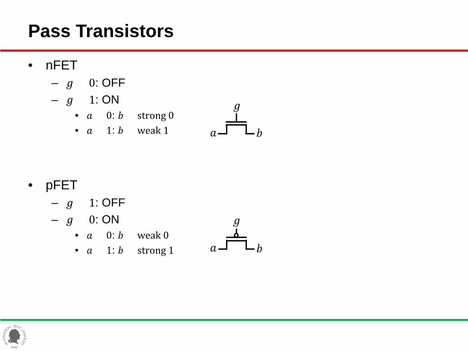
Pass Transistors
• nFET – 𝑔𝑔 = 0: OFF – 𝑔𝑔 = 1: ON
• 𝑎𝑎 = 0: 𝑏𝑏 = strong 0 • 𝑎𝑎 = 1: 𝑏𝑏 = weak 1
• pFET – 𝑔𝑔 = 1: OFF – 𝑔𝑔 = 0: ON
• 𝑎𝑎 = 0: 𝑏𝑏 = weak 0 • 𝑎𝑎 = 1: 𝑏𝑏 = strong 1
𝑔𝑔
𝑔𝑔
𝑎𝑎 𝑏𝑏
𝑎𝑎 𝑏𝑏

Transmission Gate Circuits
• Transistor circuit
• Behaviors – When 𝑠𝑠 = 0: Both nFET and pFET are OFF. – When 𝑠𝑠 = 1: Both nFET and pFET are ON.
• If 𝑥𝑥 = 0, the nFET perfectly transmits it to 𝑦𝑦 (nFET is good at transferring 0.) • If 𝑥𝑥 = 1, the pFET perfectly transmits it to 𝑦𝑦 (pFET is good at transferring 1.)
• Disadvantage
– Needs �̅�𝑠. – Does not restore the input signals.
𝑥𝑥 𝑦𝑦
𝑠𝑠
�̅�𝑠
𝑠𝑠 𝑥𝑥 𝑦𝑦
�̅�𝑠

Transmission Gate Circuits
• Logic design using transmission gates – MUX: 𝑓𝑓 = �̅�𝑠 ∙ 𝑥𝑥0 + 𝑠𝑠 ∙ 𝑥𝑥1
– XNOR
�̅�𝑠
𝑠𝑠
𝑏𝑏
𝑓𝑓
𝑥𝑥0
𝑥𝑥1
𝑓𝑓 = 𝑎𝑎⨁𝑏𝑏
𝑏𝑏�
𝑎𝑎

Pass Transistors vs. Transmission Gates
Pass TR. Transmission Gates
Symbols
Signal strength Strong 0 Weak 1
Weak 0 Strong 1
Strong 0 Strong 1
Area 𝐴𝐴 𝑟𝑟𝐴𝐴 (𝑟𝑟 > 1) 1 + 𝑟𝑟 𝐴𝐴 Control signal 𝑔𝑔 𝑔𝑔 𝑔𝑔, �̅�𝑔

Buffer
• 𝑌𝑌 = 𝐴𝐴
• Buffers are used for – Signal restoration – Interconnect optimization
𝐴𝐴 𝑌𝑌 𝐴𝐴 𝑌𝑌

Tristate Inverter
• Truth table
• Symbol & Schematic
EN Y 0 𝑍𝑍 1 �̅�𝐴
𝐴𝐴 𝑌𝑌
𝐴𝐴
𝑌𝑌
𝐸𝐸𝐴𝐴
𝐴𝐴 𝑌𝑌
𝐸𝐸𝐴𝐴
𝐸𝐸𝐴𝐴
𝐸𝐸𝐴𝐴
𝐸𝐸𝐴𝐴
𝐴𝐴

Tristate Buffer
• Symbol
• Gate-level schematic
𝐴𝐴 𝑌𝑌
𝐸𝐸𝐴𝐴
𝐴𝐴 𝑌𝑌
𝐸𝐸𝐴𝐴
𝐸𝐸𝐴𝐴
𝐴𝐴 𝑌𝑌
𝐸𝐸𝐴𝐴

Sequential Circuit – D Latch
• Positive-level-sensitive D latch CLK Q 0 hold 1 𝐴𝐴 𝑪𝑪𝑪𝑪𝑪𝑪
𝑉𝑉𝐷𝐷𝐷𝐷
𝑡𝑡
𝑉𝑉𝐷𝐷𝐷𝐷
𝑡𝑡
0
𝑫𝑫
𝑉𝑉𝐷𝐷𝐷𝐷
𝑡𝑡
𝑸𝑸
Transparent
Capture
Hold
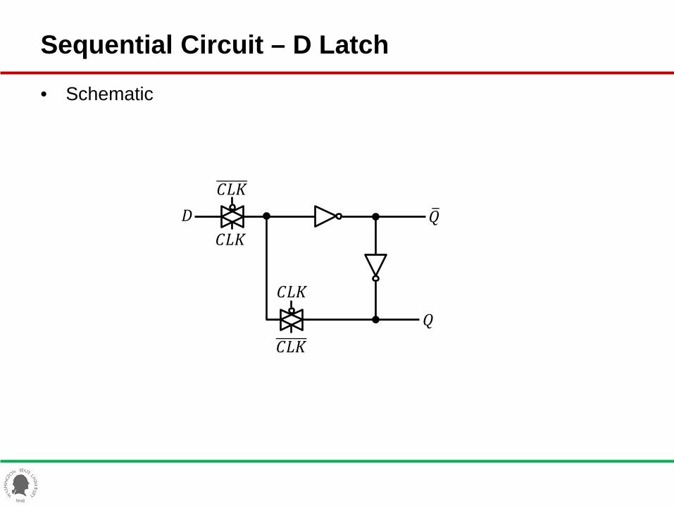
Sequential Circuit – D Latch
• Schematic
𝑄𝑄�
𝑄𝑄
𝐴𝐴 𝐶𝐶𝐶𝐶𝐶𝐶
𝐶𝐶𝐶𝐶𝐶𝐶
𝐶𝐶𝐶𝐶𝐶𝐶
𝐶𝐶𝐶𝐶𝐶𝐶
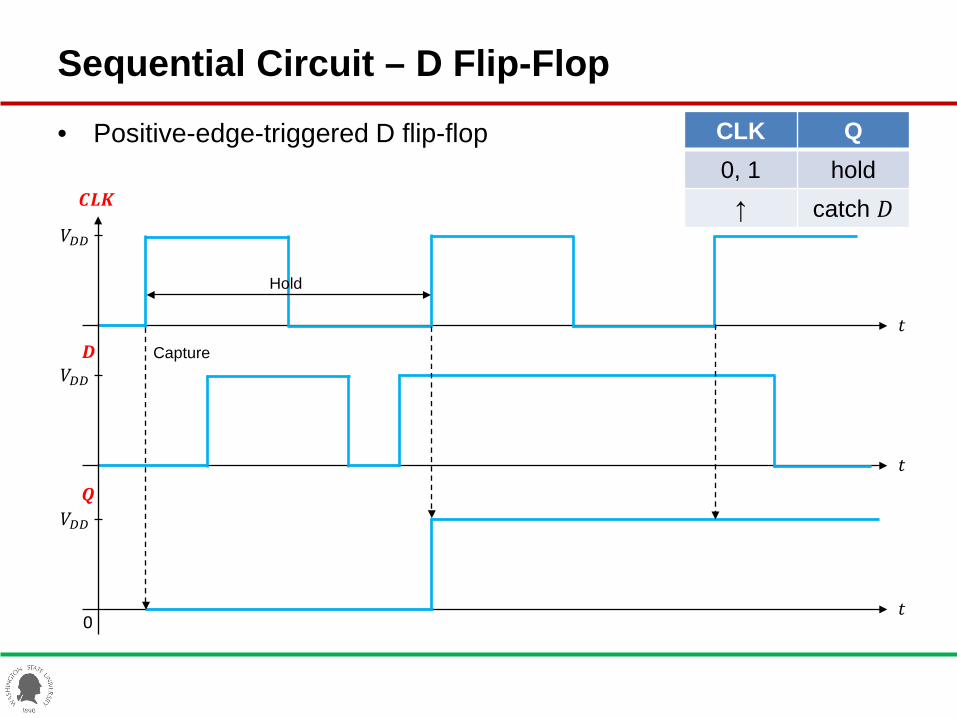
Sequential Circuit – D Flip-Flop
• Positive-edge-triggered D flip-flop
𝑉𝑉𝐷𝐷𝐷𝐷
𝑡𝑡
𝑉𝑉𝐷𝐷𝐷𝐷
𝑡𝑡
0
𝑉𝑉𝐷𝐷𝐷𝐷
𝑡𝑡
Capture
Hold
𝑪𝑪𝑪𝑪𝑪𝑪
𝑫𝑫
𝑸𝑸
CLK Q 0, 1 hold ↑ catch 𝐴𝐴

Sequential Circuit – D Flip-Flop
• Schematic
𝐴𝐴 𝐶𝐶𝐶𝐶𝐶𝐶
𝐶𝐶𝐶𝐶𝐶𝐶
𝐶𝐶𝐶𝐶𝐶𝐶
𝐶𝐶𝐶𝐶𝐶𝐶 𝑄𝑄�
𝑄𝑄 𝐶𝐶𝐶𝐶𝐶𝐶
𝐶𝐶𝐶𝐶𝐶𝐶
𝐶𝐶𝐶𝐶𝐶𝐶
𝐶𝐶𝐶𝐶𝐶𝐶

Sequential Circuit
• Example – Inputs: 𝐴𝐴,𝐴𝐴𝑂𝑂𝐴𝐴,𝐶𝐶𝐶𝐶𝐶𝐶,𝐶𝐶𝐶𝐶𝐶𝐶 – Outputs: 𝑄𝑄,𝑄𝑄�
𝑄𝑄
𝑄𝑄�
𝐶𝐶𝐶𝐶𝐶𝐶
𝐶𝐶𝐶𝐶𝐶𝐶 𝐴𝐴
𝐴𝐴𝑂𝑂𝐴𝐴
𝐶𝐶𝐶𝐶𝐶𝐶
𝐶𝐶𝐶𝐶𝐶𝐶