Embed Size (px)
Citation preview
Technical White PaperLong Term Storage Evaluation of Semiconductor Devices
Shawn Smith, Bernhard Lange, Sreenivasan Koduri, Rin Key
ABSTRACT
Since 1998, Texas Instruments and other semiconductor manufacturers have performed multiple studies regarding the storage life of semiconductor devices after assembly and test. These studies accounted for various packaging types and different plating finishes across many different products. The risks of long-term storage are documented in the 2008 publication, Component Reliability After Long Term Storage and includes a detailed risk analysis. This paper is a continuation of the assessment on devices stored between 10 and 20 years after manufacturing. JEDEC publication JEP160 outlines best practices and recommendations for the long-term storage of semiconductor products.1 The data shows that products properly stored in a controlled environment can be stored significantly greater than 15 years. Since the studies have been published, additional package families, including leadless and chip scale packaging, have been introduced. Additional tests have been performed to include these families, while also retesting the package families and finishes from prior studies. Visual inspection, solderability, cross sections, and other reliability tests were performed on the various package families to show how the long-term storage of semiconductor products does not affect the reliability or quality of the device regardless of the end use.
Table of Contents1 Introduction.............................................................................................................................................................................22 Background.............................................................................................................................................................................23 Procedure................................................................................................................................................................................ 24 Risk Assessment.................................................................................................................................................................... 25 Products Samples Included in the Evaluation.....................................................................................................................36 Packaging Materials Evaluation............................................................................................................................................ 47 Tribocharge Evaluation – ESD Testing................................................................................................................................. 68 Cover Tape Peel Strength Evaluation................................................................................................................................... 6
8.1 Test Setup.......................................................................................................................................................................... 69 Cover Tape Peel Strength Measurement Results................................................................................................................ 710 Solderability Evaluation....................................................................................................................................................... 7
10.1 Test Description................................................................................................................................................................711 Solderability Test Results.................................................................................................................................................... 9
11.1 Leadless Package............................................................................................................................................................ 911.2 SOT (Small Outline Transistor) Package....................................................................................................................... 1011.3 SOIC (Small Outline Integrated Circuit)..........................................................................................................................1111.4 QFP (Quad Flat Pack)....................................................................................................................................................1211.5 BGA (Ball Grid Array)/WCSP (Wafer Level Chip Scale Package)................................................................................. 12
12 Summary of Results........................................................................................................................................................... 1313 Conclusion.......................................................................................................................................................................... 1314 Acknowledgments.............................................................................................................................................................. 1316 References.......................................................................................................................................................................... 14
TrademarksAll trademarks are the property of their respective owners.
1 JEDEC Publication JEP160, (2011). Long-Term Storage for Electronic Solid-State Wafers, Dice, and Devices
www.ti.com Table of Contents
SLPA019 – SEPTEMBER 2021Submit Document Feedback
Long Term Storage Evaluation of Semiconductor Devices 1
Copyright © 2021 Texas Instruments Incorporated
1 IntroductionThis paper details the ongoing results of studying the quality, reliability, and usability of semiconductor products after long-term storage in a controlled environment. To better understand long-term storage viability, additional data was collected to further comprehend the time that products can be stored before the reliability can be compromised.
2 BackgroundPrior to 1995, the U.S military specified electrical retest of devices if a three-year date code window was exceeded. In 1995, the military specification MIL-PRF-19500M that mandated electrical retest after three years was revised and that requirement was removed entirely. The military now prohibits date code restrictions on component orders.2 The NEDA (National Electronic Distributor Association) "recommends that date code age restrictions be eliminated from the ordering process."2
Shelf-Life Evaluation of Nickel and Palladium Lead Finish for Integrated Circuits was published in 1998 and validated that this finish had good solderability after eight years in normal packing materials. In 2004, Shelf-Life Evaluation of Lead-Free Component Finishes concluded that the storage period for NiPdAu, NiPd, NiPdAu-Ag, matte Sn, and SnPb lead finish is >8 years as measured by solderability after exposure to a Battelle Class 2 MFG environment. The white paper Component Reliability After Long Term Storage was published in 2008 in support of the storage extension for NiPdAu leaded products >15 years and packaging materials for a minimum of six years under the worst case condition (38°C/100% RH). This was followed by BGA Package Component Reliability After Long-Term Storage in 2009 to include BGA and DSBGA/WCSP product with the long term storage conclusion of > 10 years.
In 2020, a new study validated that semiconductor products can be stored in a controlled environment for a minimum of fifteen years. The results from this study are documented in this technical white paper.
3 Procedure56 lots of product from different package types (leaded, leadless QFN style, silicon based BGA – DSBGA/WCSP and contact finishes NiPdAu, Sn, or SnAgCu solder balls) were evaluated in this study. The age of the products studied ranged from 10 years and up to 21 years of storage in a controlled environment (<30°C and <80% RH). The acronym LTS (long term storage) is used to identify this aged material.
The product packaging was carefully examined when the samples were received and the Humidity Indicator Card (HIC) was recorded for each lot at the first time opening of the sealed Moisture Barrier Bag (MBB), when applicable. The labels on the bags and boxes were evaluated for legibility and adhesion. MBB and cover tape were assessed and tested for any deterioration in ESD protection through Tribocharging testing. A cover tape peel test was performed to ensure there were no compromising attributes of the cover tape adhesion to the cover tape for long term storage.
The product underwent extensive reliability testing to determine if any adverse effects occurred while storing the devices for a long period of time. They were carefully examined for any evidence of deterioration on the lead or package body. Solderability, which can be the most significant concern with long term storage, was performed on all lots in addition to other reliability testing to determine if there were any detrimental effects.
4 Risk AssessmentThe reliability risk to semiconductor products that have been stored for longer period of time is low. In the most recent and prior studies, no evidence of diminishing reliability has been found that would adversely affect the product or the ability for it to be soldered to a PCB for material stored for a long period of time. No failure mechanisms have been identified that would compromise the electrical performance or circuit reliability of LTS devices. HTOL and HTSL qualification data provides the best estimate of parametric performance over time. Devices are biased during HTOL testing; this is the worst case compared to unbiased storage. FIT rates for analog products have been in the single digits for more than a decade. This assures that biased and unbiased devices would remain within data sheet limits far beyond the design and storage life of the device.
2 NEDA Publication, (2002). Managing Date Code Restrictions on Orders for Electronic Components
Introduction www.ti.com
2 Long Term Storage Evaluation of Semiconductor Devices SLPA019 – SEPTEMBER 2021Submit Document Feedback
Copyright © 2021 Texas Instruments Incorporated
In addition to the studies performed on the long term storage products, package qualifications include humidity testing tests to evaluate the effect of moisture on die metallization (galvanic corrosion). Devices routinely pass high temperature and high humidity testing. All products are stored in a properly controlled environment prior to being shipped. Moisture sensitive products are packaged with appropriate MBB and desiccant based on TI internal specification for moisture sensitivity which aligns with JEDEC J-STD-033C. Packaging material and cover tape was evaluated using Tribocharge testing and showed no issues. Any failure of the MBB would be detected immediately by the HIC discolorations upon opening the package.
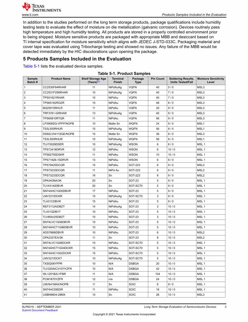
5 Products Samples Included in the EvaluationTable 5-1 lists the evaluated device samples.
Table 5-1. Product SamplesSample Batch #
Product Name Shelf Storage Age (Years)(2)
Terminal Finish
Package Type
Pin Count Soldering Results. Units Tested/Fail
Moisture Sensitivity Level
1 CC2530F64RHAR 11 NiPdAuAg VQFN 40 5 / 0 MSL3
2 CC2531F256RHAR 10 NiPdAuAg VQFN 40 7 / 0 MSL3
3 TPS51621RHAR 10 NiPdAu VQFN 40 7 / 0 MSL3
4 TPS65182RGZR 10 NiPdAu VQFN 48 8 / 0 MSL3
5 BQ25015RHLR 11 NiPdAu VQFN 20 9 / 0 MSL3
6 TRF3761-GIRHAR 13 NiPdAuAg VQFN 40 9 / 0 MSL3
7 TPS65810RTQR 11 NiPdAu VQFN 56 9 / 0 MSL3
8 LP3906SQ-VPFP/NOPB 10 Matte Sn WQFN 24 9 / 0 MSL1
9 TS3L500RHUR 15 NiPdAuAg WQFN 56 8 / 0 MSL1
10 DS92LV0411SQE/NOPB 10 Matte Sn WQFN 36 8 / 0 MSL3
11 TS3L500RHUR 10 NiPdAuAg WQFN 56 8 / 0 MSL1
12 TLV70029DSER 10 NiPdAuAg WSON 6 8 / 0 MSL 1
13 TPS73418DRVR 12 NiPdAu WSON 6 10 / 0 MSL 1
14 TPS62750DSKR 11 NiPdAu WSON 10 10 / 0 MSL 1
15 TPS71926-15DRVR 13 NiPdAu WSON 6 8 / 0 MSL 1
16 TPS79425DCQR 15 NiPdAu SOT-223 6 9 / 0 MSL2
17 TPS73233DCQR 11 NiPd Au SOT-223 6 9 / 0 MSL2
18 TPS73233DCQR 16 Sn SOT-223 6 9 / 0 MSL2
19 OPA343NA/3K 20 Sn SOT-23 5 9 / 0 MSL 1
20 TLV431AIDBVR 20 Sn SOT-SC70 5 9 / 0 MSL 1
21 SN74AHC1G00DBVR 17 NiPdAu SOT-23 5 9 / 0 MSL 1
22 LMV331IDCKR 15 NiPdAuAg SOT-SC70 3 9 / 0 MSL 1
23 TL431CDBVR 15 NiPdAu SOT-23 5 9 / 0 MSL 1
24 REF3112AIDBZT 14 NiPdAuAg SOT-23 3 10 / 0 MSL 1
25 TL431QDBVT 10 NiPdAu SOT-23 5 10 / 0 MSL 1
26 TLV809J25DBZT 10 NiPdAu SOT-23 3 10 / 0 MSL 1
27 SN74LVC1G06DBVR 10 NiPdAu SOT-23 5 10 / 0 MSL 1
28 SN74AHCT1G86DBVR 10 NiPdAu SOT-23 5 10 / 0 MSL 1
29 ADS7868IDBVR 10 NiPdAu SOT-23 6 10 / 0 MSL2
30 OPA2337EA/3K 11 Sn SOT-23 8 10 / 0 MSL2
31 SN74LVC1G08DCKR 10 NiPdAu SOT-SC70 5 10 / 0 MSL 1
32 SN74AHCT1G04DCKR 15 NiPdAu SOT-SC70 5 10 / 0 MSL 1
33 SN74AHC1G02DCKR 15 NiPdAu SOT-SC70 5 10 / 0 MSL 1
34 LMV321IDCKT 10 NiPdAuAg SOT-SC70 5 10 / 0 MSL 1
35 TXS0206YFPR 10 N/A DSBGA 20 10 / 0 MSL 1
36 TLV320AIC3107IYZFR 10 N/A DSBGA 42 10 / 0 MSL 1
37 WL1251B2LYFBR 11 N/A DSBGA 104 10 / 0 MSL 1
38 PCM1870YZFR 12 n/a DSBGA 24 10 / 0 MSL 1
39 LMV641MAX/NOPB 11 Sn SOIC 8 9 / 0 MSL 1
40 SN74HC595DR 11 NiPdAu SOIC 16 10 / 0 MSL 1
41 USBN9604-28MX 10 Sn SOIC 28 10 / 0 MSL3
www.ti.com Products Samples Included in the Evaluation
SLPA019 – SEPTEMBER 2021Submit Document Feedback
Long Term Storage Evaluation of Semiconductor Devices 3
Copyright © 2021 Texas Instruments Incorporated
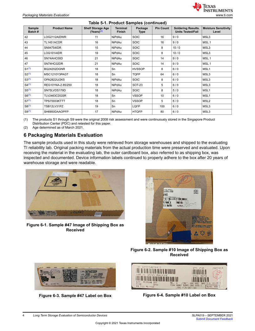
Table 5-1. Product Samples (continued)Sample Batch #
Product Name Shelf Storage Age (Years)(2)
Terminal Finish
Package Type
Pin Count Soldering Results. Units Tested/Fail
Moisture Sensitivity Level
42 LOG2112AIDWR 11 NiPdAu SOIC 16 9 / 0 MSL3
43 TL1451ACDR 16 NiPdAu SOIC 16 9 / 0 MSL 1
44 SN94754IDR 15 NiPdAu SOIC 8 10 / 0 MSL3
45 LOG101AIDR 19 NiPdAu SOIC 8 10 / 0 MSL3
46 SN74AHC00D 21 NiPdAu SOIC 14 9 / 0 MSL 1
47 SN74HC02DR 21 NiPdAu SOIC 14 9 / 0 MSL 1
S1(1) BQ24202DGNR 18 Sn HVSSOP 8 6 / 0 MSL1
S2(1) MSC1210Y3PAGT 18 Sn TQFP 64 6 / 0 MSL3
S3(1) OPA2822U/2K5 18 NiPdAu SOIC 8 6 / 0 MSL3
S4(1) REG101NA-2.85/250 18 NiPdAu SOT-23 5 6 / 0 MSL3
S5(1) SN75LVDS179D 18 NiPdAu SOIC 8 5 / 0 MSL1
S6(1) TLV2463CDGSR 18 Sn VSSOP 10 6 / 0 MSL1
S7(1) TPS75933KTTT 18 Sn VSSOP 5 6 / 0 MSL2
S8(1) TSB12LV31PZ 19 Sn LQFP 100 6 / 0 MSL3
S9(1) SH6950DAAOPFP 17 NiPdAu HTQFP 80 6 / 0 MSL3
(1) The products S1 through S9 were the original 2008 risk assessment and were continuously stored in the Singapore Product Distribution Center (PDC) and retested for this paper.
(2) Age determined as of March 2021.
6 Packaging Materials EvaluationThe sample products used in this study were retrieved from storage warehouses and shipped to the evaluating TI reliability lab. Original packing materials from the actual production time were preserved and evaluated. Upon receiving the material in the evaluating lab, the outer cardboard box, also referred to as shipping box, was inspected and documented. Device information labels continued to properly adhere to the box after 20 years of warehouse storage and were readable.
Figure 6-1. Sample #47 Image of Shipping Box as Received
Figure 6-2. Sample #10 Image of Shipping Box as Received
Figure 6-3. Sample #47 Label on Box Figure 6-4. Sample #10 Label on Box
Packaging Materials Evaluation www.ti.com
4 Long Term Storage Evaluation of Semiconductor Devices SLPA019 – SEPTEMBER 2021Submit Document Feedback
Copyright © 2021 Texas Instruments Incorporated
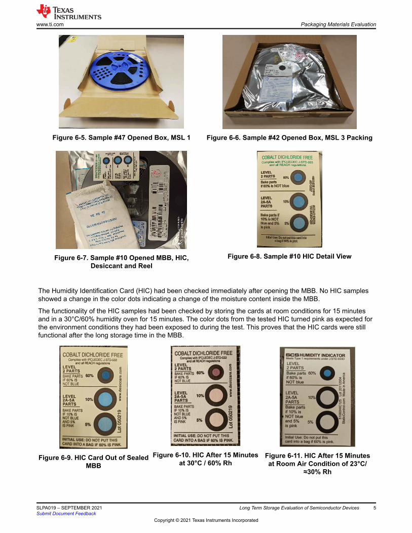
Figure 6-5. Sample #47 Opened Box, MSL 1 Figure 6-6. Sample #42 Opened Box, MSL 3 Packing
Figure 6-7. Sample #10 Opened MBB, HIC, Desiccant and Reel
Figure 6-8. Sample #10 HIC Detail View
The Humidity Identification Card (HIC) had been checked immediately after opening the MBB. No HIC samples showed a change in the color dots indicating a change of the moisture content inside the MBB.
The functionality of the HIC samples had been checked by storing the cards at room conditions for 15 minutes and in a 30°C/60% humidity oven for 15 minutes. The color dots from the tested HIC turned pink as expected for the environment conditions they had been exposed to during the test. This proves that the HIC cards were still functional after the long storage time in the MBB.
Figure 6-9. HIC Card Out of Sealed MBB
Figure 6-10. HIC After 15 Minutes at 30°C / 60% Rh
Figure 6-11. HIC After 15 Minutes at Room Air Condition of 23°C/
≈30% Rh
www.ti.com Packaging Materials Evaluation
SLPA019 – SEPTEMBER 2021Submit Document Feedback
Long Term Storage Evaluation of Semiconductor Devices 5
Copyright © 2021 Texas Instruments Incorporated
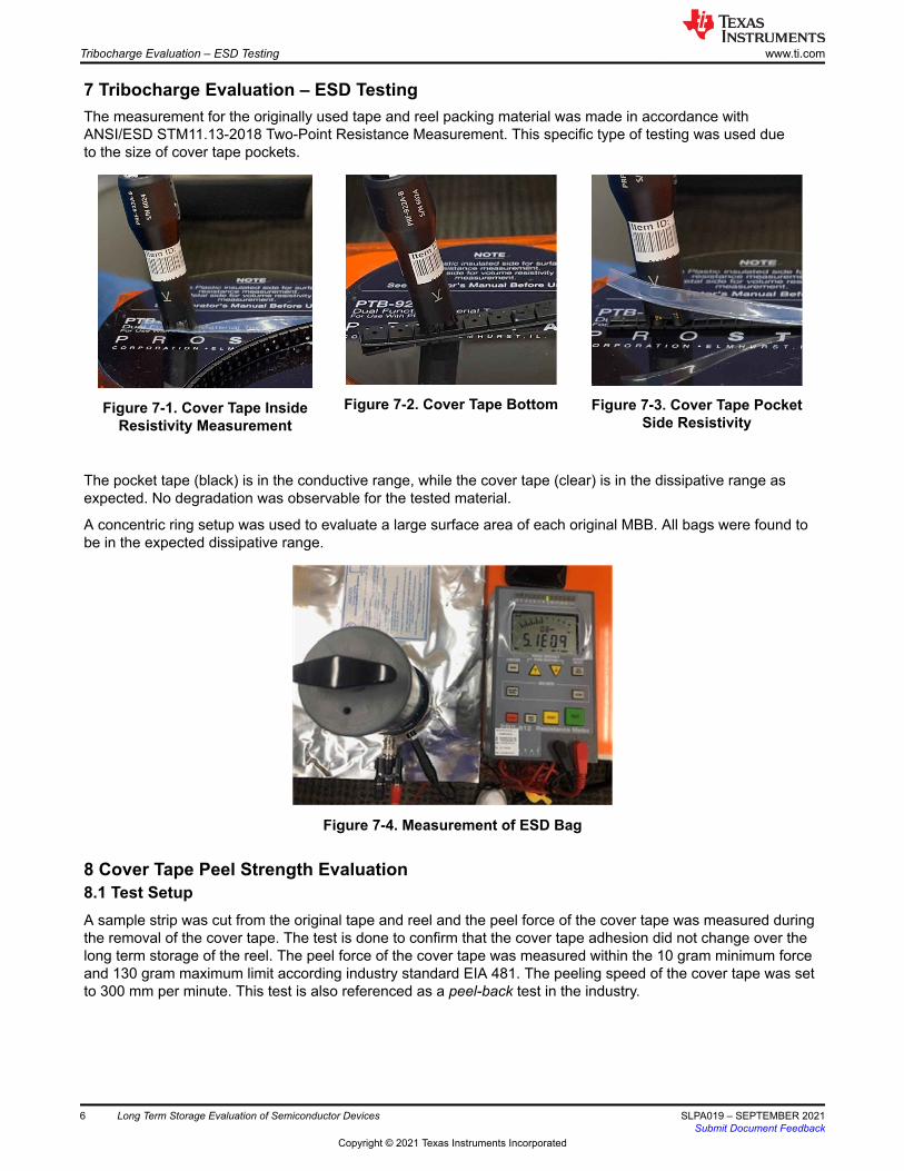
7 Tribocharge Evaluation – ESD TestingThe measurement for the originally used tape and reel packing material was made in accordance with ANSI/ESD STM11.13-2018 Two-Point Resistance Measurement. This specific type of testing was used due to the size of cover tape pockets.
Figure 7-1. Cover Tape Inside Resistivity Measurement
Figure 7-2. Cover Tape Bottom Figure 7-3. Cover Tape Pocket Side Resistivity
The pocket tape (black) is in the conductive range, while the cover tape (clear) is in the dissipative range as expected. No degradation was observable for the tested material.
A concentric ring setup was used to evaluate a large surface area of each original MBB. All bags were found to be in the expected dissipative range.
Figure 7-4. Measurement of ESD Bag
8 Cover Tape Peel Strength Evaluation8.1 Test SetupA sample strip was cut from the original tape and reel and the peel force of the cover tape was measured during the removal of the cover tape. The test is done to confirm that the cover tape adhesion did not change over the long term storage of the reel. The peel force of the cover tape was measured within the 10 gram minimum force and 130 gram maximum limit according industry standard EIA 481. The peeling speed of the cover tape was set to 300 mm per minute. This test is also referenced as a peel-back test in the industry.
Tribocharge Evaluation – ESD Testing www.ti.com
6 Long Term Storage Evaluation of Semiconductor Devices SLPA019 – SEPTEMBER 2021Submit Document Feedback
Copyright © 2021 Texas Instruments Incorporated
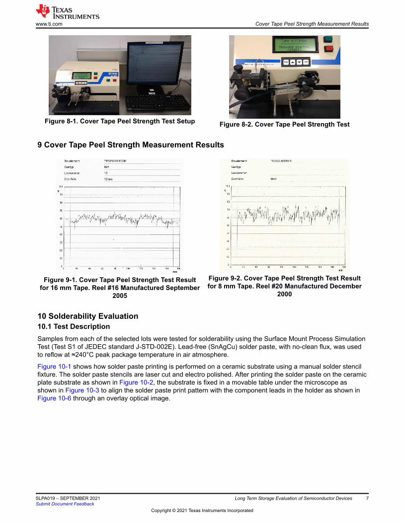
Figure 8-1. Cover Tape Peel Strength Test Setup Figure 8-2. Cover Tape Peel Strength Test
9 Cover Tape Peel Strength Measurement Results
Figure 9-1. Cover Tape Peel Strength Test Result for 16 mm Tape. Reel #16 Manufactured September
2005
Figure 9-2. Cover Tape Peel Strength Test Result for 8 mm Tape. Reel #20 Manufactured December
2000
10 Solderability Evaluation10.1 Test DescriptionSamples from each of the selected lots were tested for solderability using the Surface Mount Process Simulation Test (Test S1 of JEDEC standard J-STD-002E). Lead-free (SnAgCu) solder paste, with no-clean flux, was used to reflow at ≈240°C peak package temperature in air atmosphere.
Figure 10-1 shows how solder paste printing is performed on a ceramic substrate using a manual solder stencil fixture. The solder paste stencils are laser cut and electro polished. After printing the solder paste on the ceramic plate substrate as shown in Figure 10-2, the substrate is fixed in a movable table under the microscope as shown in Figure 10-3 to align the solder paste print pattern with the component leads in the holder as shown in Figure 10-6 through an overlay optical image.
www.ti.com Cover Tape Peel Strength Measurement Results
SLPA019 – SEPTEMBER 2021Submit Document Feedback
Long Term Storage Evaluation of Semiconductor Devices 7
Copyright © 2021 Texas Instruments Incorporated
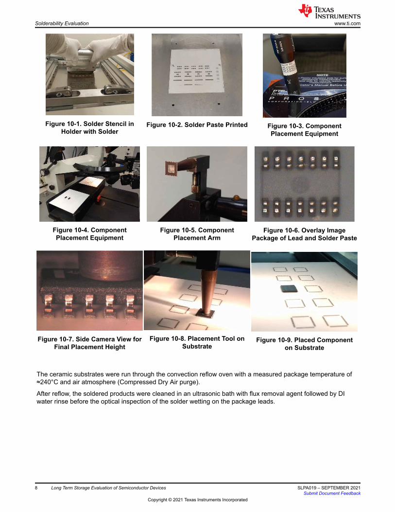
Figure 10-1. Solder Stencil in Holder with Solder
Figure 10-2. Solder Paste Printed Figure 10-3. Component Placement Equipment
Figure 10-4. Component Placement Equipment
Figure 10-5. Component Placement Arm
Figure 10-6. Overlay Image Package of Lead and Solder Paste
Figure 10-7. Side Camera View for Final Placement Height
Figure 10-8. Placement Tool on Substrate
Figure 10-9. Placed Component on Substrate
The ceramic substrates were run through the convection reflow oven with a measured package temperature of ≈240°C and air atmosphere (Compressed Dry Air purge).
After reflow, the soldered products were cleaned in an ultrasonic bath with flux removal agent followed by DI water rinse before the optical inspection of the solder wetting on the package leads.
Solderability Evaluation www.ti.com
8 Long Term Storage Evaluation of Semiconductor Devices SLPA019 – SEPTEMBER 2021Submit Document Feedback
Copyright © 2021 Texas Instruments Incorporated
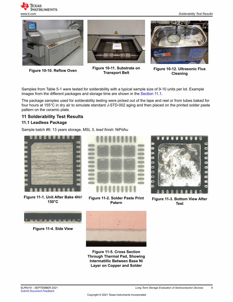
Figure 10-10. Reflow Oven Figure 10-11. Substrate on Transport Belt
Figure 10-12. Ultrasonic Flux Cleaning
Samples from Table 5-1 were tested for solderability with a typical sample size of 9-10 units per lot. Example images from the different packages and storage time are shown in the Section 11.1.
The package samples used for solderability testing were picked out of the tape and reel or from tubes baked for four hours at 155°C in dry air to simulate standard J-STD-002 aging and then placed on the printed solder paste pattern on the ceramic plate.
11 Solderability Test Results11.1 Leadless PackageSample batch #6: 13 years storage, MSL 3, lead finish: NiPdAu
Figure 11-1. Unit After Bake 4Hr/150°C
Figure 11-2. Solder Paste Print Patern
Figure 11-3. Bottom View After Test
Figure 11-4. Side View
Figure 11-5. Cross Section Through Thermal Pad, Showing Intermatillic Between Base Ni Layer on Copper and Solder
www.ti.com Solderability Test Results
SLPA019 – SEPTEMBER 2021Submit Document Feedback
Long Term Storage Evaluation of Semiconductor Devices 9
Copyright © 2021 Texas Instruments Incorporated
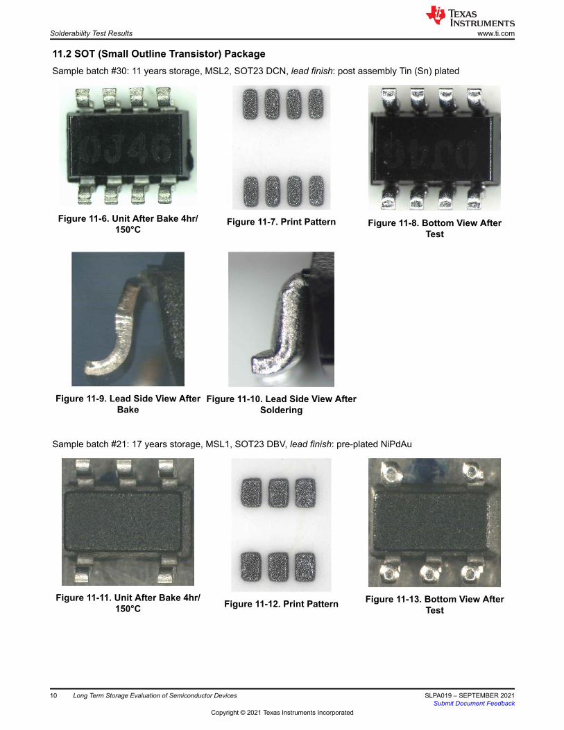
11.2 SOT (Small Outline Transistor) PackageSample batch #30: 11 years storage, MSL2, SOT23 DCN, lead finish: post assembly Tin (Sn) plated
Figure 11-6. Unit After Bake 4hr/150°C
Figure 11-7. Print Pattern Figure 11-8. Bottom View After Test
Figure 11-9. Lead Side View After Bake
Figure 11-10. Lead Side View After Soldering
Sample batch #21: 17 years storage, MSL1, SOT23 DBV, lead finish: pre-plated NiPdAu
Figure 11-11. Unit After Bake 4hr/150°C Figure 11-12. Print Pattern Figure 11-13. Bottom View After
Test
Solderability Test Results www.ti.com
10 Long Term Storage Evaluation of Semiconductor Devices SLPA019 – SEPTEMBER 2021Submit Document Feedback
Copyright © 2021 Texas Instruments Incorporated
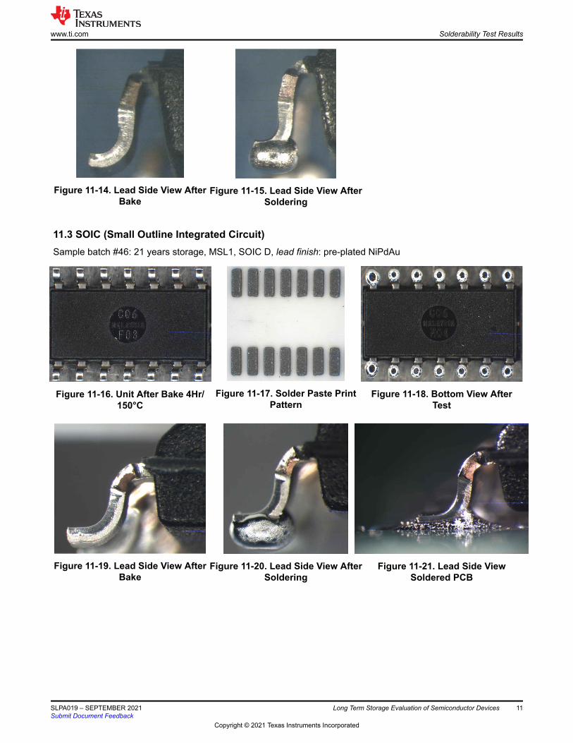
Figure 11-14. Lead Side View After Bake
Figure 11-15. Lead Side View After Soldering
11.3 SOIC (Small Outline Integrated Circuit)Sample batch #46: 21 years storage, MSL1, SOIC D, lead finish: pre-plated NiPdAu
Figure 11-16. Unit After Bake 4Hr/150°C
Figure 11-17. Solder Paste Print Pattern
Figure 11-18. Bottom View After Test
Figure 11-19. Lead Side View After Bake
Figure 11-20. Lead Side View After Soldering
Figure 11-21. Lead Side View Soldered PCB
www.ti.com Solderability Test Results
SLPA019 – SEPTEMBER 2021Submit Document Feedback
Long Term Storage Evaluation of Semiconductor Devices 11
Copyright © 2021 Texas Instruments Incorporated
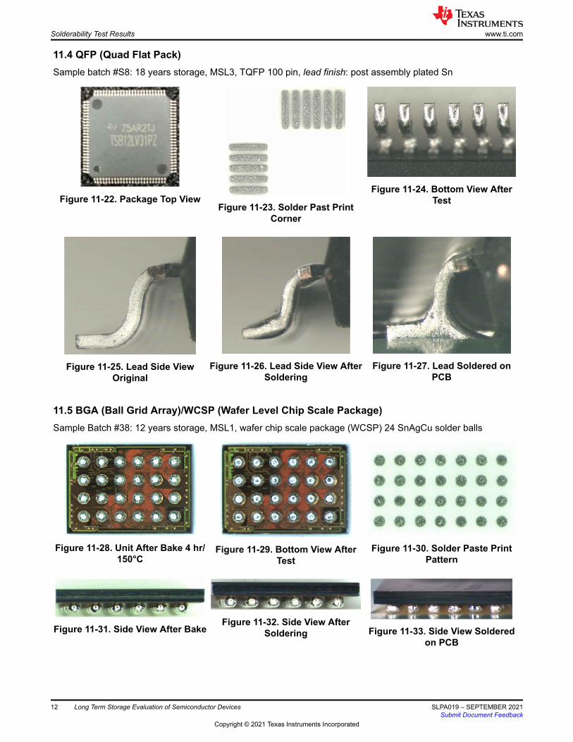
11.4 QFP (Quad Flat Pack)Sample batch #S8: 18 years storage, MSL3, TQFP 100 pin, lead finish: post assembly plated Sn
Figure 11-22. Package Top ViewFigure 11-23. Solder Past Print
Corner
Figure 11-24. Bottom View After Test
Figure 11-25. Lead Side View Original
Figure 11-26. Lead Side View After Soldering
Figure 11-27. Lead Soldered on PCB
11.5 BGA (Ball Grid Array)/WCSP (Wafer Level Chip Scale Package)Sample Batch #38: 12 years storage, MSL1, wafer chip scale package (WCSP) 24 SnAgCu solder balls
Figure 11-28. Unit After Bake 4 hr/150°C
Figure 11-29. Bottom View After Test
Figure 11-30. Solder Paste Print Pattern
Figure 11-31. Side View After BakeFigure 11-32. Side View After
Soldering Figure 11-33. Side View Soldered on PCB
Solderability Test Results www.ti.com
12 Long Term Storage Evaluation of Semiconductor Devices SLPA019 – SEPTEMBER 2021Submit Document Feedback
Copyright © 2021 Texas Instruments Incorporated
12 Summary of Results• Reliability of the semiconductor devices stored in an environmentally controlled warehouse for an extended
period of time up to 21 years was assessed. No failure mechanisms were identified.• ESD performance of tape and reel samples was comparable to new tape and pocket samples.• The HIC were confirmed to be functional after LTS.• The desiccant used for moisture sensitive product is active for >15 years.• No degradation in ESD performance or moisture ingress was observed on the MBB when stored in a
controlled environment.• Solderability of the package pins met all expectations and is comparable with the solderability performance of
current devices.
13 ConclusionAdvancements in lead-frame technology, packing materials, work methods, and inventory logistics have made it possible to further extend the time between manufacturing semiconductor products and delivering to customers. This extended storage time does not impact product performance or the customers product shelf life. In multiple studies performed since 1998, no evidence of diminishing reliability has been found that would adversely affect the product or the ability for it to be soldered to a PCB. No failure mechanisms have been identified that would compromise the circuit reliability of LTS devices. Based on these studies, TI will eliminate limitations on the storage durations. TI will continue to collect data on more samples and as the data directs, TI will continue to adjust the storage conditions and duration for various products.
14 AcknowledgmentsThe author wishes to recognize the following individuals and groups for their professional assistance:
• Andreas Pfeiffer and Markus Filbry, TI Germany, solderability testing and documentation of the 2020 long term storage study results.
• TI technical staff members who collaborated and contributed to the evaluation efforts.• The TI Reliability Laboratory in Freising, Germany and Dallas, Texas.• Dallas Device Analysis Operation (DDAO) and Freising Device Analysis Operation (FDAO).• Todd Wyant, TI Dallas, packaging support.• Ron Eller, TI Dallas, technical assistance.• Ron Madsen, TI Tucson, retired.
www.ti.com Summary of Results
SLPA019 – SEPTEMBER 2021Submit Document Feedback
Long Term Storage Evaluation of Semiconductor Devices 13
Copyright © 2021 Texas Instruments Incorporated
15 Glossary of TermsBGA Ball Grid Array Package – a package with solder balls (globules) attached at the
package bottom side for electrical contact.Desiccant A hygroscopic substance used to remove moisture from moisture barrier bags.Humidity Indicator Card
(HIC) – a card printed with a moisture sensitive chemical (cobalt chloride) that changes from blue to pink in the presence of water vapor.
Long Term Storage (LTS) – storage of devices in an uncontrolled indoor environment for more than two years. In some publication also Extended Shelf Life (ESL) is used.
Moisture Barrier Bag (MBB) – storage bag manufactured with a flexible laminated vapor barrier film that restricts transmission of water vapor (also called Dry Pack Back).
Nickel, Palladium, Gold
(NiPdAu) – metal layers that are pre-plated on leadframes to enable solderability.
NiPdAu Nickel, palladium, gold – composition of lead finish which is plated on the bare copper leadframe with nickel being the first on the copper and followed by palladium and gold plating step.
NiPdAuAg Is a variation in the industry where the AuAg plating is a composition in the plating bath.QFN Quad Flat no Leads package – a package with flat contact areas at the package bottom
for electrical contacts.QFP Quad Flat package – a package with formed metal leads at the package sides for
electrical contacts.SAC / SnAgCu Solder paste metal composition, tin, silver, copper content.Shelf Life The time that moisture sensitive devices may be stored in MBB with desiccant and HIC
or MSL 1 devices stored at room ambient.Sn Tin, composition of lead finish which is plated on the bare copper leadframe surfaces
extending the package after the package encapsulation process completed.SOIC Small Outline Integrated Circuit package – a package with formed metal leads at the
package sides for electrical contacts.SOT Small Outline Transistor Package – a package with formed metal leads at the package
sides for electrical contacts.Water Vapor Transmission Rate
(WVTR) – a measure of permeability of MBBs to water vapor.
WCSP Wafer Chip Scale Package or Die Size BGA – silicon die with attached solder balls or globules at the bottom of the package for electrical contact.
16 References1. JEDEC Publication JEP160, (2011). Long-Term Storage for Electronic Solid-State Wafers, Dice, and
Devices. Retrieved from https://www.jedec.org/standards-documents/2. NEDA Publication, (2002). Managing Date Code Restrictions on Orders for Electronic Components.
Retrieved from https://www.ecianow.org/assets/docs/GIPC/3. Texas Instruments, BGA Package Component Reliability After Long-Term Storage application note4. Texas Instruments, Component Reliability After Long Term Storage technical white papers5. Texas Instruments, Shelf-Life Evaluation of Lead-Free Component Finishes application reports6. Texas Instruments, Shelf -Life Evaluation of Nickel/Palladium Lead Finish for Integrated Circuits application
reports
Glossary of Terms www.ti.com
14 Long Term Storage Evaluation of Semiconductor Devices SLPA019 – SEPTEMBER 2021Submit Document Feedback
Copyright © 2021 Texas Instruments Incorporated
IMPORTANT NOTICE AND DISCLAIMERTI PROVIDES TECHNICAL AND RELIABILITY DATA (INCLUDING DATASHEETS), DESIGN RESOURCES (INCLUDING REFERENCEDESIGNS), APPLICATION OR OTHER DESIGN ADVICE, WEB TOOLS, SAFETY INFORMATION, AND OTHER RESOURCES “AS IS”AND WITH ALL FAULTS, AND DISCLAIMS ALL WARRANTIES, EXPRESS AND IMPLIED, INCLUDING WITHOUT LIMITATION ANYIMPLIED WARRANTIES OF MERCHANTABILITY, FITNESS FOR A PARTICULAR PURPOSE OR NON-INFRINGEMENT OF THIRDPARTY INTELLECTUAL PROPERTY RIGHTS.These resources are intended for skilled developers designing with TI products. You are solely responsible for (1) selecting the appropriateTI products for your application, (2) designing, validating and testing your application, and (3) ensuring your application meets applicablestandards, and any other safety, security, or other requirements. These resources are subject to change without notice. TI grants youpermission to use these resources only for development of an application that uses the TI products described in the resource. Otherreproduction and display of these resources is prohibited. No license is granted to any other TI intellectual property right or to any third partyintellectual property right. TI disclaims responsibility for, and you will fully indemnify TI and its representatives against, any claims, damages,costs, losses, and liabilities arising out of your use of these resources.TI’s products are provided subject to TI’s Terms of Sale (https:www.ti.com/legal/termsofsale.html) or other applicable terms available eitheron ti.com or provided in conjunction with such TI products. TI’s provision of these resources does not expand or otherwise alter TI’sapplicable warranties or warranty disclaimers for TI products.IMPORTANT NOTICE
Mailing Address: Texas Instruments, Post Office Box 655303, Dallas, Texas 75265Copyright © 2021, Texas Instruments Incorporated


![Semiconductor Devices [Kanaan Kano]](https://img.pdfslide.net/doc/110x75/55cf931a550346f57b9bb747/semiconductor-devices-kanaan-kano.jpg)