Embed Size (px)
Citation preview
International Research Journal of Engineering and Technology (IRJET) e-ISSN: 2395 -0056
Volume: 03 Issue: 08 | Aug-2016 www.irjet.net p-ISSN: 2395-0072
© 2016, IRJET | Impact Factor value: 4.45 | ISO 9001:2008 Certified Journal | Page 1831
Low Dropout (LDO) Regulator with Feed-Forward Ripple Cancellation
Technique
SULTANA BEGUM1, BASAVARAJ P G2, NAGARAJ P3
1PG Scholar VLSI Design and Embedded System, VTU, VTU Extension Centre, UTL technologies LTD, Bangalore 2 PG Scholar VLSI Design and Embedded System, VTU, VTU Extension Centre, UTL technologies LTD, Bangalore
3 Assistant Professor, VLSI Design and Embedded System, VTU Extension Centre, UTL technologies LTD, Bangalore
---------------------------------------------------------------------***---------------------------------------------------------------------
Abstract - A Low Drop-Out (LDO) regulator is designed with a technique called feed-forward ripple cancellation (FFRC). In a wide frequency range, the FFRC-LDO attains a high Power-Supply Rejection Ratio (PSRR). In this work all design stages and analysis of the FFRC-LDO are completed. The LDO is implemented in 180nm CMOS technology in cadence virtuoso environment and designed to attain a PSRR of -51 dB at 15MHz with cascoding technique for load currents up to 25mA with the total power consumption of 127.76mW. To complete the FFRC-LDO Regulator Error amplifier, Feed-Forward amplifier and Summing amplifier, are designed and implemented. The gain of error amplifier and feed-forward amplifier achieved greater than 24dB. A LDO schematic and layout has been designed.
Key Words: DC to DC converter, Low Drop-Out Regulator, Complementary MOS, Feed-Forward Ripples Cancellation, Power Supply Rejection Ratio (PSRR). 1. INTRODUCTION
In power management, the Low Drop-Out (LDO) regulator is significant building block, which trails a DC-DC switching converter, as illustrates in Fig.1 [1]. LDO is used to regulate supply ripples to offer a constant steady voltage source for analog/RF blocks which are noise-sensitive. By CMOS technologies, the main objective of designing a LDO which attains high power-supply rejection Ratio (PSRR) for a wide range of load conditions.
Now-a-days an integrating power management
system into single on-chip is in more demand. Hence, operating frequency of switching converters is growing to consent advanced level of integration [5]. So, therefore the succeeding LDO should afford high PSRR up to switching frequencies which leads to an increase in the frequency of ripples at the output. For large frequencies greater than 300 kHz, traditional LDOs have poor PSRR. The main reasons for poor PSR are: Finite output conductance of the pass transistor. To attain better regulation, the low DC gain of submicron technologies which require complex gain phases. Finite bandwidth of the feedback path.
This paper presents a Cascode Stage LNA, which is well suited for biomedical applications as it operates at the frequency of 915MHz i.e. ISM band and also suited for low power applications. This amplifier is responsible for amplifying the bio signals, and has to offer low input referred noise and low power consumption.
Figure 1: Block diagram of power management system
To increase the PSRR there are some methods. They
are: By RC filtering at the LDOs output [6], the input ripples of the LDO can be degrades and leads to a large area consumption and drop-out voltage which does not suite for low-voltage technologies. Cascading two regulators [6]. Along with RC filtering, cascade other transistor with pass transistor (PMOS) [8]-[10], by some special methods such as drain-extended FET devices and charge-pump techniques to bias the gate of any of transistors. Conversely, large current supply because of the high voltage drop across the resistance increases the drop-out voltage in LDO and area. Charge pump procedure upturns complexity and power dissipation is more because along with RC filtering a clock is needed to eliminate clock ripples.
All earlier techniques which have been proposed focused only on the idea is to deliver much isolation along the high-current signal path from the input to output. In addition, at low frequencies these systems afford high PSRR, but the frequencies up to some MHz, they are incapable of offering enough PSRR (greater than -50 dB).
To overwhelm by the limitations of earlier projected PSRR LDO regulators, an introduction of a high PSRR low voltage LDO regulator based on a feed-forward ripple cancellation (FFRC) approach. The LDO topology reserves conventional loop dynamics structure, even though delivering high PSRR for a wide frequency range. It also
International Research Journal of Engineering and Technology (IRJET) e-ISSN: 2395 -0056
Volume: 03 Issue: 08 | Aug-2016 www.irjet.net p-ISSN: 2395-0072
© 2016, IRJET | Impact Factor value: 4.45 | ISO 9001:2008 Certified Journal | Page 1832
empowers the design for high supply currents and low quiescent current consumption.
2. FFRC DESIGN OF LDO
At low frequencies the PSRR can be boosted by swelling the LDO’s feedback gain. Though at higher frequencies, the PSRR is restricted by the dominant pole of the feedback loop. To attain higher PSRR at both DC gain and higher frequencies, the ripples must be eliminated.
A. BASIC CONCEPT
A zero transfer gain is needed to remove input ripples seeming at the output. In the ideal case, this is attained by implementing a feed-forward path that duplicates same input ripples at the gate of the pass transistor (Mp). Hence, the gate-overdrive voltage is independent of input ripples and no ripples appear across the load. In the actual case, part of the ripples leak through the finite output resistance of Mp and must be removed. In the LDO system feed-forward path is be implemented by feed-forward amplifier and summing amplifier.
Figure 2: Block level demonstration of FFR LDO.
Using the traditional architecture, the achieved PSRR is less than 60dB [8] and it begins to decrease nearby 330 KHz. This frequency is observed at the dominant pole of the error amplifier. The PSRR at DC gain is boosted by 20dB using FFRC-LDO. Due the supplementary zero that increases the frequency at which the PSRR starts to rise at 9MHz.
At first, the PSRR begins to rise about 330 KHz, which is bandwidth of the error amplifier. The key advantage of this FFRC approach is attaining a high PSRR without a need of increasing the bandwidth and therefore the quiescent power consumption over a wide range of frequency. Furthermore, this approach conserves the same low drop-out voltage of a conventional regulator, since supply rejection does not occur on high current signal path. The gain of both feed-forward and summing amplifiers is depends on the ratio of resistors to decrease the addiction of process-temperature (PT) deviations [7]. At low frequencies the PSRR has its greatest value for a current of 5mA.
As current upturns, PSRR is starts to decrease because of the DC gain dependency of Mp on the output current and the transistor operating point changes to linear region. Later the DC gain is condensed. The biasing voltage of the summing amplifier has to be adjusted such that the output DC voltage of the summing amplifier is greater than zero.
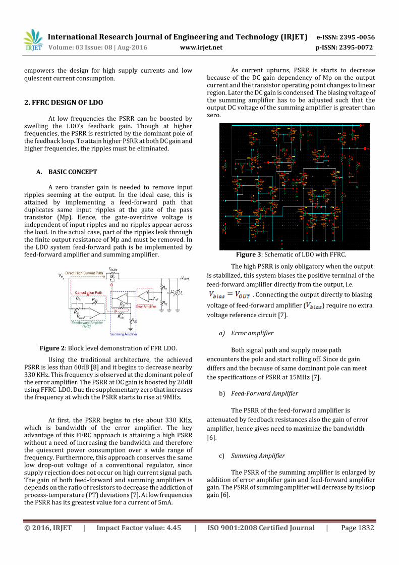
Figure 3: Schematic of LDO with FFRC. The high PSRR is only obligatory when the output
is stabilized, this system biases the positive terminal of the
feed-forward amplifier directly from the output, i.e.
. Connecting the output directly to biasing
voltage of feed-forward amplifier ( ) require no extra
voltage reference circuit [7].
a) Error amplifier
Both signal path and supply noise path
encounters the pole and start rolling off. Since dc gain
differs and the because of same dominant pole can meet
the specifications of PSRR at 15MHz [7].
b) Feed-Forward Amplifier
The PSRR of the feed-forward amplifier is
attenuated by feedback resistances also the gain of error
amplifier, hence gives need to maximize the bandwidth
[6].
c) Summing Amplifier
The PSRR of the summing amplifier is enlarged by addition of error amplifier gain and feed-forward amplifier gain. The PSRR of summing amplifier will decrease by its loop gain [6].
International Research Journal of Engineering and Technology (IRJET) e-ISSN: 2395 -0056
Volume: 03 Issue: 08 | Aug-2016 www.irjet.net p-ISSN: 2395-0072
© 2016, IRJET | Impact Factor value: 4.45 | ISO 9001:2008 Certified Journal | Page 1833
B. STABILITY
Preferably, the stability of the LDO does not effect by the feed-forward path, because the feed-forward path does not exist in the feedback loop. However in this
implementation, the node of feed-forward amplifier is connected to remove the need for another reference voltage.
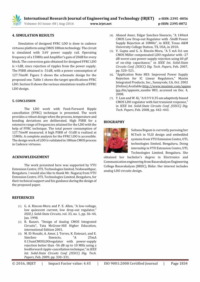
3. RESULTS AND DESIGN ANALYSIS
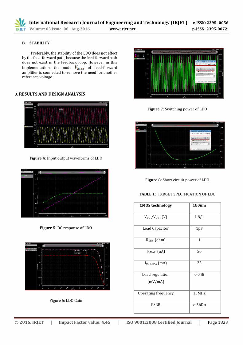
Figure 4: Input output waveforms of LDO
Figure 5: DC response of LDO
Figure 6: LDO Gain
Figure 7: Switching power of LDO
Figure 8: Short circuit power of LDO
TABLE 1: TARGET SPECIFICATION OF LDO
CMOS technology 180nm
VDD /VOUT (V) 1.8/1
Load Capacitor 1pF
RSER (ohm) 1
IQ,MAX (uA) 50
IOUT,MAX (mA) 25
Load regulation
(mV/mA)
0.048
Operating frequency 15MHz
PSRR >-56Db
International Research Journal of Engineering and Technology (IRJET) e-ISSN: 2395 -0056
Volume: 03 Issue: 08 | Aug-2016 www.irjet.net p-ISSN: 2395-0072
© 2016, IRJET | Impact Factor value: 4.45 | ISO 9001:2008 Certified Journal | Page 1834
4. SIMULATION RESULTS
Simulation of designed FFRC LDO is done in cadence
virtuoso platform using CMOS 180nm technology. The circuit
is simulated with 3.6V power supply rail. Operating
frequency of a 15MHz and Amplifier’s gain of 20dB for every
block. The conversion gain obtained for designed FFRC LDO
is >1dB, since rejection of ripples from the power supply. The PSRR obtained is -51dB, with a power consumption of
127.76mW. Figure 3 shows the schematic design for the
proposed one. Table 1 shows the target specifications FFRC
LDO. Section II shows the various simulation results of FFRC
LDO design.
5. CONCLUSION
The LDO work with Feed-Forward Ripple cancellation (FFRC) technique is presented. The work provides a robust design when the process, temperature and bonding deviations are deliberated. High PSRR for a extensive range of frequencies attained for the LDO with the help of FFRC technique. The total power consumption of 127.76mW measured. A high PSRR of -51dB is realized at 15MHz. A complete analysis for the FFRC LDO is accessible. The design work of LDO is validated in 180nm CMOS process in Cadence virtuoso.
ACKNOWLEDGEMENT
The work presented here was supported by VTU Extension Centre, UTL Technologies limited, Yeshwanthpur, Bengaluru. I would also like to thank Mr. Nagaraj from VTU Extension Centre, UTL Technologies Limited, Bengaluru, for their technical support and his guidance during the design of the proposed paper.
REFERENCES
[1]. G. A. Rincon-Mora and P. E. Allen, “A low-voltage, low quiescent current, low drop-out regulator,” IEEE J. Solid-State Circuits, vol. 33, no. 1, pp. 36–44, Jan. 1998.
[2]. B. Razavi, “Design of Analog CMOS Integrated Circuits”, Tata McGraw-Hill Higher Education, international Edition 2001.
[3]. M. El-Nozahi, A. Amer, J. Torres, K. Entesari, and E. Sánchez- Sinencio, “A 25mA 0.13umCMOSLDOregulator with power-supply rejection better than -56 dB up to 10 MHz using a feedforward ripple-cancellation technique,” in IEEE Int. Solid-State Circuits Conf. (ISSCC) Dig. Tech. Papers, Feb. 2009, pp. 330–331.
[4]. Ahmed Amer, Edgar Sanchez-Sinencio, “A 140mA CMOS Low Drop-out Regulator with -56dB Power Supply Rejection at 10MHz”, in IEEE, Texas A&M University College Station, TX, USA, in 2010.
[5]. V. Gupta and G. A. Rincón-Mora, “A 5 mA 0.6 um CMOS Miller compensated LDO regulator with -27 dB worst-case power-supply rejection using 60 pF of on-chip capacitance,” in IEEE Int. Solid-State Circuits Conf. (ISSCC) Dig. Tech. Papers, Feb. 2007, pp. 520–521.
[6]. “Application Note 883: Improved Power Supply Rejection for IC Linear Regulators,” Maxim Integrated Products, Inc., Sunnyvale, CA, Oct. 2002 [Online].Available:http://www.maximic.com/appnotes.cfm/appnote_numbe 883, accessed on Dec. 4, 2008.
[7]. Y. Lam and W. Ki, “A 0.9 V 0.35 um adaptively biased CMOS LDO regulator with fast transient response,” in IEEE Int. Solid-State Circuits Conf. (ISSCC) Dig. Tech. Papers, Feb. 2008, pp. 442–443.
BIOGRAPHY
Sultana Begum is currently pursuing her
M.Tech in VLSI design and embedded
systems from VTU Extension Centre, UTL
technologies limited, Bengaluru, Doing
internship in VTU Extension Centre, UTL
Technologies Limited, Bengaluru. She
obtained her bachelor’s degree in Electronics and
Communication engineering from Basavakalyan Engineering
College Basavakalyan (BKEC), Bidar. Her interest includes
analog LDO circuits design.


![Design of Low-Dropout Regulator - allresearchjournal.com · Proposed LDO design converts an input voltage of 1 V to tunable ... Regulators [1] and switching regulator [10]. In this](https://img.pdfslide.net/doc/110x75/5b91ca6e09d3f26a278c82ed/design-of-low-dropout-regulator-proposed-ldo-design-converts-an-input-voltage.jpg)