Embed Size (px)
Citation preview
PCM3008
SLAS332 – APRIL 2001
LOW POWER AND LOW VOLTAGE 16-BIT, SINGLE-ENDEDANALOG INPUT/OUTPUT STEREO AUDIO CODEC
1www.ti.com
FEATURES 16-Bit Delta-Sigma ADC and DAC
Stereo ADC:– Single-Ended Voltage Input– Anti-Aliasing Filter Included– High Performance
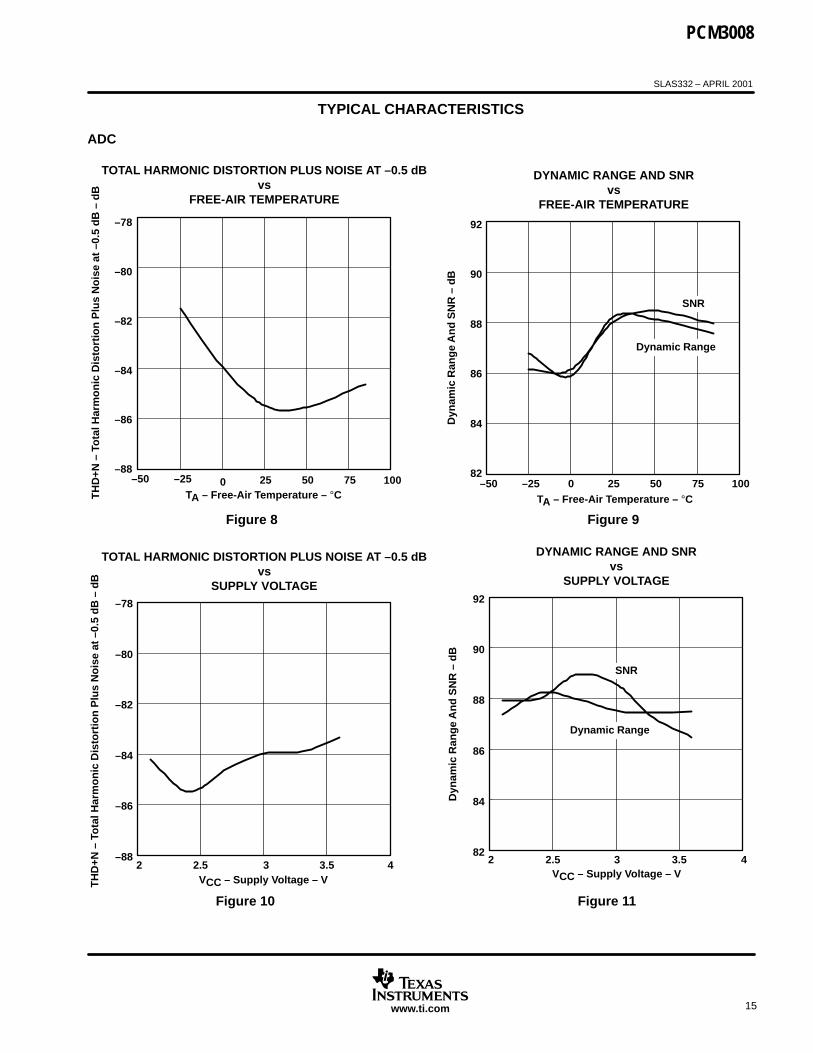
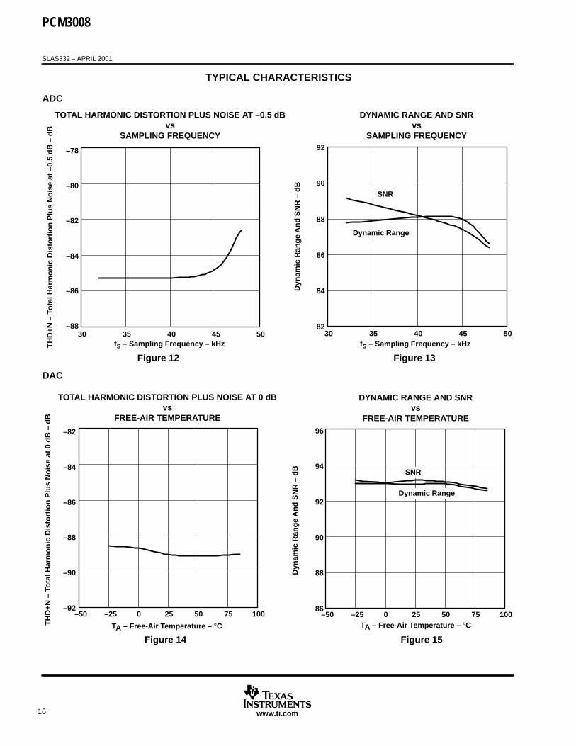
– THD+N: –84 dB– SNR: 88 dB– Dynamic Range: 88 dB
– 1/64× Decimation Digital Filter– Passband Ripple: ±0.05 dB– Stopband Attenuation: –65 dB
– Digital HPF Included
Stereo DAC:– Single-Ended Voltage Output– Analog LPF and FIR Filter Included– High Performance
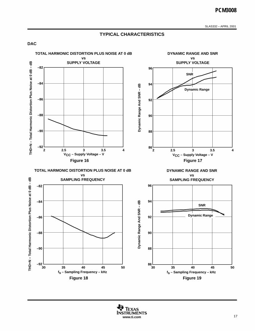
– THD+N: –88 dB– SNR: 92 dB– Dynamic Range: 92 dB
– 8× Oversampling Digital Filter– Passband Ripple: ±0.1 dB– Stopband Attenuation: –43 dB
Audio Data Format:– ADC: 16-bit, Left-Justified– DAC: 16-bit, Right-Justified
Special Built-In Functions:– Digital De-Emphasis: 32, 44.1, 48 kHz– ADC/DAC Independent Power Down With
Pop-Noise Free Muting
Sampling Rate: 8 kHz to 48 kHz
System Clock: 256fS, 384fS, 512fS Low Voltage Power Supply:
– 2.4 V TYP, 2.1 V MIN to 3.6 V MAX
Low Power Dissipation:– 32 mW at VCC = 2.4 V
Package: 16-Pin TSSOP
APPLICATIONS Digital Video Camera
Portable MD Player
Other Portable System
DESCRIPTION
The PCM3008 is a low cost single chip 16-bitstereo audio codec with single-ended analogvoltage input and output.
Both ADCs and DACs employ delta-sigmamodulation with 64-times oversampling. ADCsinclude a digital decimation filter and digital highpass filter. DACs include an 8-times oversamplingdigital interpolation filter, digital de-emphasis filterand pop-noise free muting which works during thepower down ON/OFF sequence. The PCM3008accepts left-justified format for ADC, andright-justified format for DAC. Independentpower-down modes for ADC and DAC areprovided.
The PCM3008 is suitable for a wide variety ofcost-sensitive consumer applications where goodperformance is required. It is fabricated using ahighly advanced CMOS process and is availablein a small 16-pin TSSOP package.
PRODUCTION DATA information is current as of publication date.Products conform to specifications per the terms of Texas Instrumentsstandard warranty. Production processing does not necessarily includetesting of all parameters.
Copyright 2001, Texas Instruments Incorporated
Please be aware that an important notice concerning availability, standard warranty, and use in critical applications ofTexas Instruments semiconductor products and disclaimers thereto appears at the end of this data sheet.
PCM3008
SLAS332 – APRIL 2001
2 www.ti.com
1
2
3
4
5
6
78
16
15
14
13
12
11
109
VCOMVINRVINLGNDVCC
DEM0DEM1DOUT
VOUTRVOUTLPDDAPDADBCKSYSCKLRCKDIN
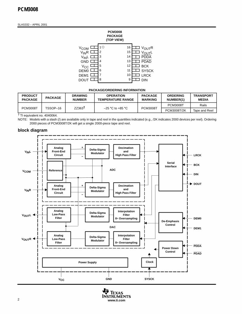
PCM3008PACKAGE
(TOP VIEW)
PACKAGE/ORDERING INFORMATION
PRODUCTPACKAGE PACKAGE
DRAWINGNUMBER
OPERATIONTEMPERATURE RANGE
PACKAGEMARKING
ORDERINGNUMBER(1)
TRANSPORTMEDIA
° °PCM3008T Rails
PCM3008T TSSOP–16 ZZ363 –25 °C to +85 °C PCM3008TPCM3008T/2K Tape and Reel
† TI equivalent no. 4040064.NOTE: Models with a slash (/) are available only in tape and reel in the quantities indicated (e.g., /2K indicates 2000 devices per reel). Ordering
2000 pieces of PCM3008T/2K will get a single 2000-piece tape and reel.
block diagram
ClockPower Supply
Reference ADC
DAC
AnalogFront-End
Circuit
Delta-SigmaModulator
+
–
Decimationand
High Pass Filter
SerialInterface
AnalogFront-End
Circuit
Delta-SigmaModulator
Decimationand
High Pass Filter
+
–
AnalogLow-Pass
Filter
AnalogLow-Pass
Filter
Delta-SigmaModulator
Delta-SigmaModulator
InterpolationFilter
8× Oversampling
InterpolationFilter
8× Oversampling
De-EmphasisControl
Power DownControl
VINL
VCOM
VINR
VOUTL
VOUTR
VCC GND SYSCK
LRCK
BCK
DIN
DOUT
DEM0
DEM1
PDDA
PDAD
PCM3008
SLAS332 – APRIL 2001
3www.ti.com
_
+_
+ DeltaSigma
Modulator
+
–
30 kΩ2
1
VINR
VCOM
+
0.47 µF
+1 µF
Reference
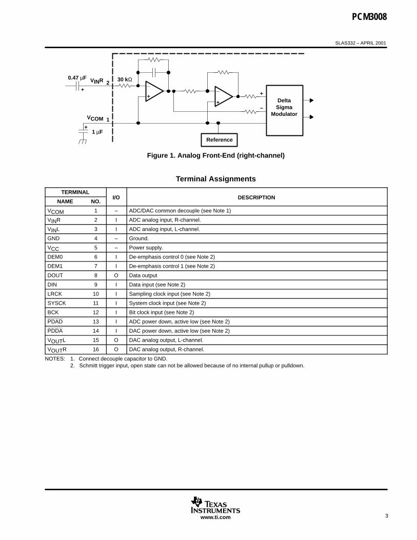
Figure 1. Analog Front-End (right-channel)
Terminal Assignments
TERMINAL
NAME NO.I/O DESCRIPTION
VCOM 1 – ADC/DAC common decouple (see Note 1)
VINR 2 I ADC analog input, R-channel.
VINL 3 I ADC analog input, L-channel.
GND 4 – Ground.
VCC 5 – Power supply.
DEM0 6 I De-emphasis control 0 (see Note 2)
DEM1 7 I De-emphasis control 1 (see Note 2)
DOUT 8 O Data output
DIN 9 I Data input (see Note 2)
LRCK 10 I Sampling clock input (see Note 2)
SYSCK 11 I System clock input (see Note 2)
BCK 12 I Bit clock input (see Note 2)
PDAD 13 I ADC power down, active low (see Note 2)
PDDA 14 I DAC power down, active low (see Note 2)
VOUTL 15 O DAC analog output, L-channel.
VOUTR 16 O DAC analog output, R-channel.
NOTES: 1. Connect decouple capacitor to GND.2. Schmitt trigger input, open state can not be allowed because of no internal pullup or pulldown.
PCM3008
SLAS332 – APRIL 2001
4 www.ti.com
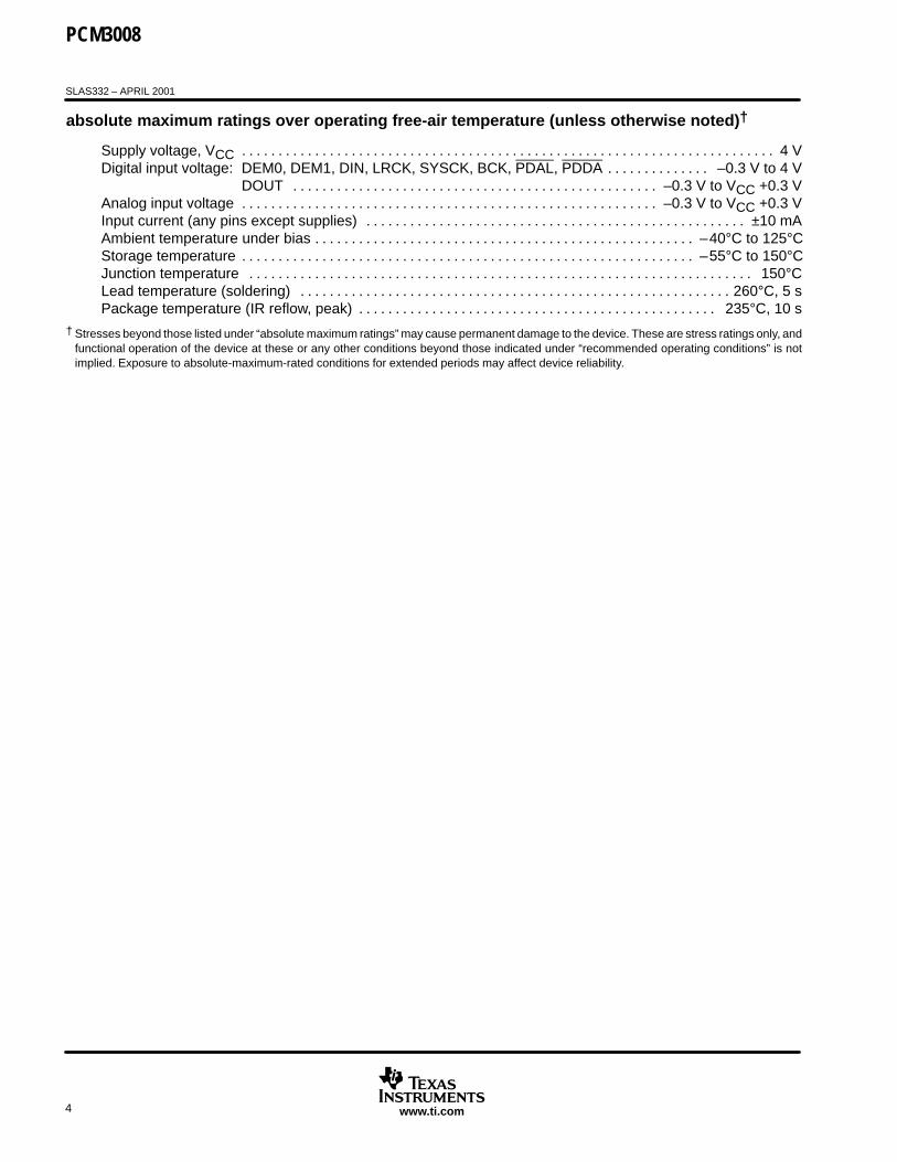
absolute maximum ratings over operating free-air temperature (unless otherwise noted)†
Supply voltage, VCC 4 V. . . . . . . . . . . . . . . . . . . . . . . . . . . . . . . . . . . . . . . . . . . . . . . . . . . . . . . . . . . . . . . . . . . . . . . . . Digital input voltage: DEM0, DEM1, DIN, LRCK, SYSCK, BCK, PDAL, PDDA –0.3 V to 4 V. . . . . . . . . . . . . .
DOUT –0.3 V to VCC +0.3 V. . . . . . . . . . . . . . . . . . . . . . . . . . . . . . . . . . . . . . . . . . . . . . . . . . Analog input voltage –0.3 V to VCC +0.3 V. . . . . . . . . . . . . . . . . . . . . . . . . . . . . . . . . . . . . . . . . . . . . . . . . . . . . . . . . Input current (any pins except supplies) ±10 mA. . . . . . . . . . . . . . . . . . . . . . . . . . . . . . . . . . . . . . . . . . . . . . . . . . . . Ambient temperature under bias –40°C to 125°C. . . . . . . . . . . . . . . . . . . . . . . . . . . . . . . . . . . . . . . . . . . . . . . . . . . . Storage temperature –55°C to 150°C. . . . . . . . . . . . . . . . . . . . . . . . . . . . . . . . . . . . . . . . . . . . . . . . . . . . . . . . . . . . . . Junction temperature 150°C. . . . . . . . . . . . . . . . . . . . . . . . . . . . . . . . . . . . . . . . . . . . . . . . . . . . . . . . . . . . . . . . . . . . . Lead temperature (soldering) 260°C, 5 s. . . . . . . . . . . . . . . . . . . . . . . . . . . . . . . . . . . . . . . . . . . . . . . . . . . . . . . . . . . Package temperature (IR reflow, peak) 235°C, 10 s. . . . . . . . . . . . . . . . . . . . . . . . . . . . . . . . . . . . . . . . . . . . . . . . .
† Stresses beyond those listed under “absolute maximum ratings” may cause permanent damage to the device. These are stress ratings only, andfunctional operation of the device at these or any other conditions beyond those indicated under “recommended operating conditions” is notimplied. Exposure to absolute-maximum-rated conditions for extended periods may affect device reliability.
PCM3008
SLAS332 – APRIL 2001
5www.ti.com
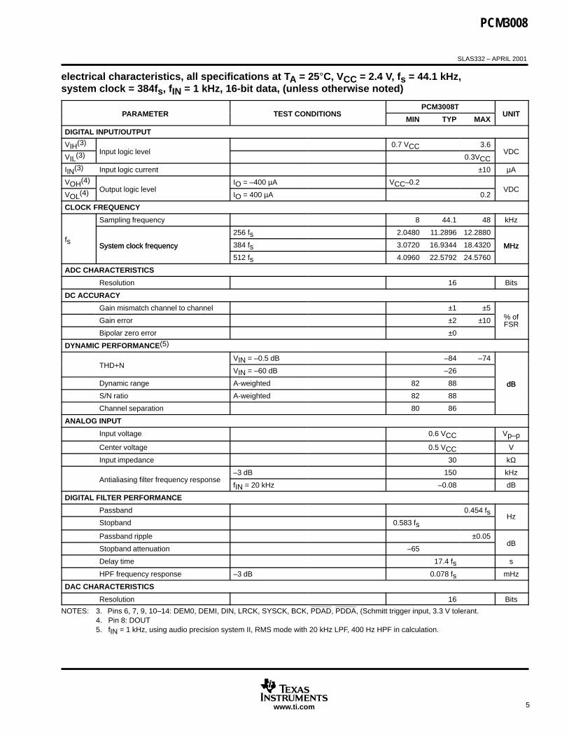
electrical characteristics, all specifications at TA = 25°C, VCC = 2.4 V, fs = 44.1 kHz, system clock = 384fs, fIN = 1 kHz, 16-bit data, (unless otherwise noted)
PCM3008TPARAMETER TEST CONDITIONS
MIN TYP MAXUNIT
DIGITAL INPUT/OUTPUT
VIH(3) 0.7 VCC 3.6
VIL(3) Input logic level0.3VCC
VDC
IIN(3) Input logic current ±10 µA
VOH(4) IO = –400 µA VCC–0.2
VOL(4) Output logic levelIO = 400 µA 0.2
VDC
CLOCK FREQUENCY
Sampling frequency 8 44.1 48 kHz
256 fs 2.0480 11.2896 12.2880fs
System clock frequency 384 fs 3.0720 16.9344 18.4320 MHzSystem clock frequency
512 fs 4.0960 22.5792 24.5760
MHz
ADC CHARACTERISTICS
Resolution 16 Bits
DC ACCURACY
Gain mismatch channel to channel ±1 ±5
Gain error ±2 ±10 % of
Bipolar zero error ±0FSR
DYNAMIC PERFORMANCE(5)
VIN = –0.5 dB –84 –74THD+N
VIN = –60 dB –26
Dynamic range A-weighted 82 88 dB
S/N ratio A-weighted 82 88
dB
Channel separation 80 86
ANALOG INPUT
Input voltage 0.6 VCC Vp–p
Center voltage 0.5 VCC V
Input impedance 30 kΩ
–3 dB 150 kHzAntialiasing filter frequency response
fIN = 20 kHz –0.08 dB
DIGITAL FILTER PERFORMANCE
Passband 0.454 fsStopband 0.583 fs
Hz
Passband ripple ±0.05
Stopband attenuation –65dB
Delay time 17.4 fs s
HPF frequency response –3 dB 0.078 fs mHz
DAC CHARACTERISTICS
Resolution 16 Bits
NOTES: 3. Pins 6, 7, 9, 10–14: DEM0, DEMI, DIN, LRCK, SYSCK, BCK, PDAD, PDDA, (Schmitt trigger input, 3.3 V tolerant.4. Pin 8: DOUT5. fIN = 1 kHz, using audio precision system II, RMS mode with 20 kHz LPF, 400 Hz HPF in calculation.
PCM3008
SLAS332 – APRIL 2001
6 www.ti.com
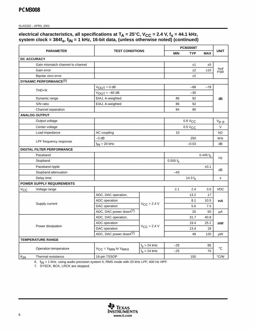
electrical characteristics, all specifications at TA = 25°C, VCC = 2.4 V, fs = 44.1 kHz, system clock = 384fs, fIN = 1 kHz, 16-bit data, (unless otherwise noted) (continued)
PCM3008TPARAMETER TEST CONDITIONS
MIN TYP MAXUNIT
DC ACCURACY
Gain mismatch channel to channel ±1 ±5
Gain error ±2 ±10 %of
Bipolar zero error ±2FSR
DYNAMIC PERFORMANCE(6)
VOUT = 0 dB –88 –78THD+N
VOUT = –60 dB –30
Dynamic range EIAJ, A-weighted 86 92 dB
S/N ratio EIAJ, A-weighted 86 92
dB
Channel separation 84 90
ANALOG OUTPUT
Output voltage 0.6 VCC Vp–p
Center voltage 0.5 VCC V
Load impedance AC coupling 10 kΩ
–3 dB 250 kHzLPF frequency response
fIN = 20 kHz –0.03 dB
DIGITAL FILTER PERFORMANCE
Passband 0.445 fsStopband 0.555 fs
Hz
Passband ripple ±0.1
Stopband attenuation –43dB
Delay time 14.3 fs s
POWER SUPPLY REQUIREMENTS
VCC Voltage range 2.1 2.4 3.6 VDC
ADC, DAC operation, 13.2 17
ADC operation 8.1 10.5 mASupply current
DAC operationVCC = 2.4 V
5.6 7.5
mA
ADC, DAC power down(7) 20 50 µA
ADC, DAC operation, 31.7 40.8
ADC operation 19.4 25.2 mWPower dissipation
DAC operationVCC = 2.4 V
13.4 18
mW
ADC, DAC power down(7) 48 120 µW
TEMPERATURE RANGE
fs > 24 kHz –25 85°Operation temperature VCC = VMIN to VMAX fs < 24 kHz –25 70°C
θJA Thermal resistance 16-pin TSSOP 150 °C/W
6. fIN = 1 kHz, using audio precision system II, RMS mode with 20 kHz LPF, 400 Hz HPF.7. SYSCK, BCK, LRCK are stopped.

PCM3008
SLAS332 – APRIL 2001
7www.ti.com
theory of operation
ADC section
The PCM3008 ADC consists of a reference circuit, a stereo single-to-differential converter, a stereo fullydifferential 5th-order delta-sigma modulator, a digital decimation filter with high pass filter function and a serialinterface circuit. The block diagram in this data sheet illustrates the architecture of the ADC section and Figure1 shows the single-to-differential converter.
An internal reference circuit with one external capacitor provides all reference voltages required by the ADCand DAC. The internal single-to-differential voltage converter saves the design, space and extra parts neededfor external circuitry required by many delta-sigma converters. The internal full-differential signal processingarchitecture provides a wide dynamic range and excellent power supply rejection performance. The input signalis sampled at 64× oversampling rate, eliminating the need for a sample-and-hold circuit, and simplifyinganti-alias filtering requirements. The 5th-order delta-sigma noise shaper consists of five integrators that use aswitched-capacitor topology, a comparator and a feedback loop consisting of a one-bit DAC. The delta-sigmamodulator shapes the quantization noise, shifting it out of the audio band in the frequency domain.
The 64fs one-bit data stream from the modulator is converted to 1fs 16-bit data words by the decimation filter,which also acts as a low pass filter to remove the shaped quantization noise. The dc components are removedby a high pass filter function contained within the decimation filter.
DAC section
The PCM3008 DAC consists of a serial interface circuit, a 8× digital interpolation filter with de-emphasis filterfunction, a stereo 5th-order delta-sigma modulator, and a stereo analog FIR filter with LPF and output bufferamplifier. The block diagram in this data sheet illustrates the architecture of the DAC section. 1fs 16-bit audiodata is converted to 8fs 18-bit data by an 8× oversampling interpolation filter, and then converted to 64fs one-bitdata by delta-sigma modulator. One-bit digital data is converted to an analog signal by a current source D toA, and then high frequency components of the shaped quantization noise out of band is reduced by the analogFIR filter and LPF. The fade in, fade out function in digital domain, and VOUT control circuit in analog domainprovide a pop-noise free muting function that is required for the power down on/off control sequence.
system clock
The system clock for PCM3008 must be either 256fs, 384fs or 512fs, where fs is the audio sampling frequency.The system clock must be supplied on SYSCK (pin 11). PCM3008 also has a system clock detection circuit thatautomatically senses 256fs, 384fs or 512fs mode, and when 384fs or 512fs system clock is used, the clock isdivided into 256fs automatically. The 256fs clock is used to operate the digital filter and the modulator. Thesystem clock must be supplied whenever power is applied and either PDAD or PDDA is HIGH, as the PCM3008uses dynamic circuits internally. Table 1 lists the relationship of typical sampling frequency and system clockfrequency, and Figure 2 illustrates the system clock timing.
tSCKL1/256 fs, 1/384 fs or 1/512 fs
0.7 VCC
0.3 VCC
tSCKH
H
LSYSCK
SYMBOL DEFINITION MIN UNIT
tSCKH System clock pulse width HIGH 15 ns
tSCKL System clock pulse width LOW 15 ns
Figure 2. System Clock Timing
PCM3008
SLAS332 – APRIL 2001
8 www.ti.com
system clock (continued)
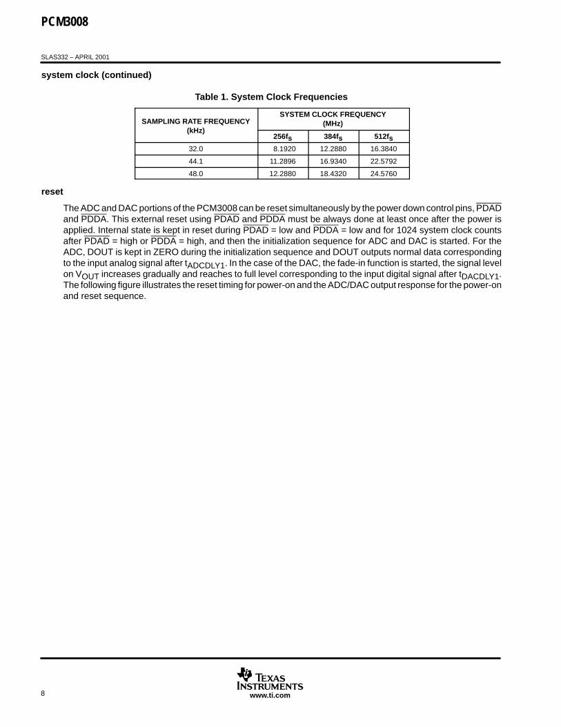
Table 1. System Clock Frequencies
SAMPLING RATE FREQUENCYSYSTEM CLOCK FREQUENCY
(MHz)(kHz)
256fs 384fs 512fs32.0 8.1920 12.2880 16.3840
44.1 11.2896 16.9340 22.5792
48.0 12.2880 18.4320 24.5760
reset
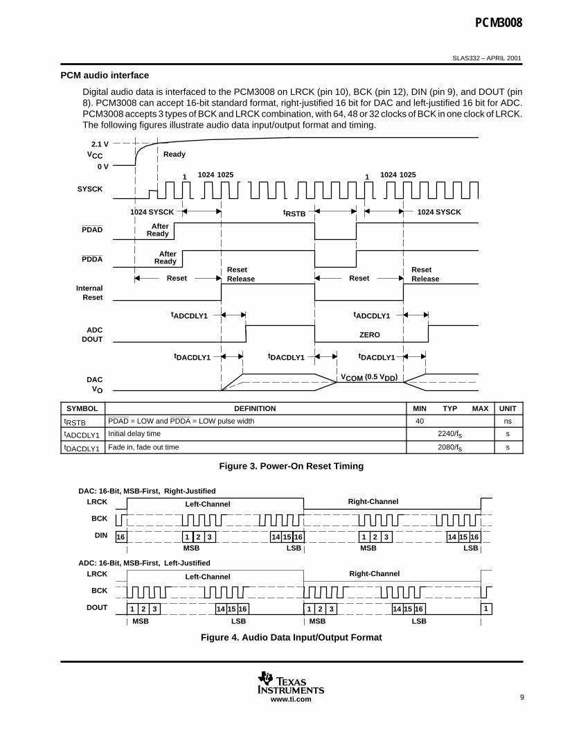
The ADC and DAC portions of the PCM3008 can be reset simultaneously by the power down control pins, PDADand PDDA. This external reset using PDAD and PDDA must be always done at least once after the power isapplied. Internal state is kept in reset during PDAD = low and PDDA = low and for 1024 system clock countsafter PDAD = high or PDDA = high, and then the initialization sequence for ADC and DAC is started. For theADC, DOUT is kept in ZERO during the initialization sequence and DOUT outputs normal data correspondingto the input analog signal after tADCDLY1. In the case of the DAC, the fade-in function is started, the signal levelon VOUT increases gradually and reaches to full level corresponding to the input digital signal after tDACDLY1.The following figure illustrates the reset timing for power-on and the ADC/DAC output response for the power-onand reset sequence.
PCM3008
SLAS332 – APRIL 2001
9www.ti.com
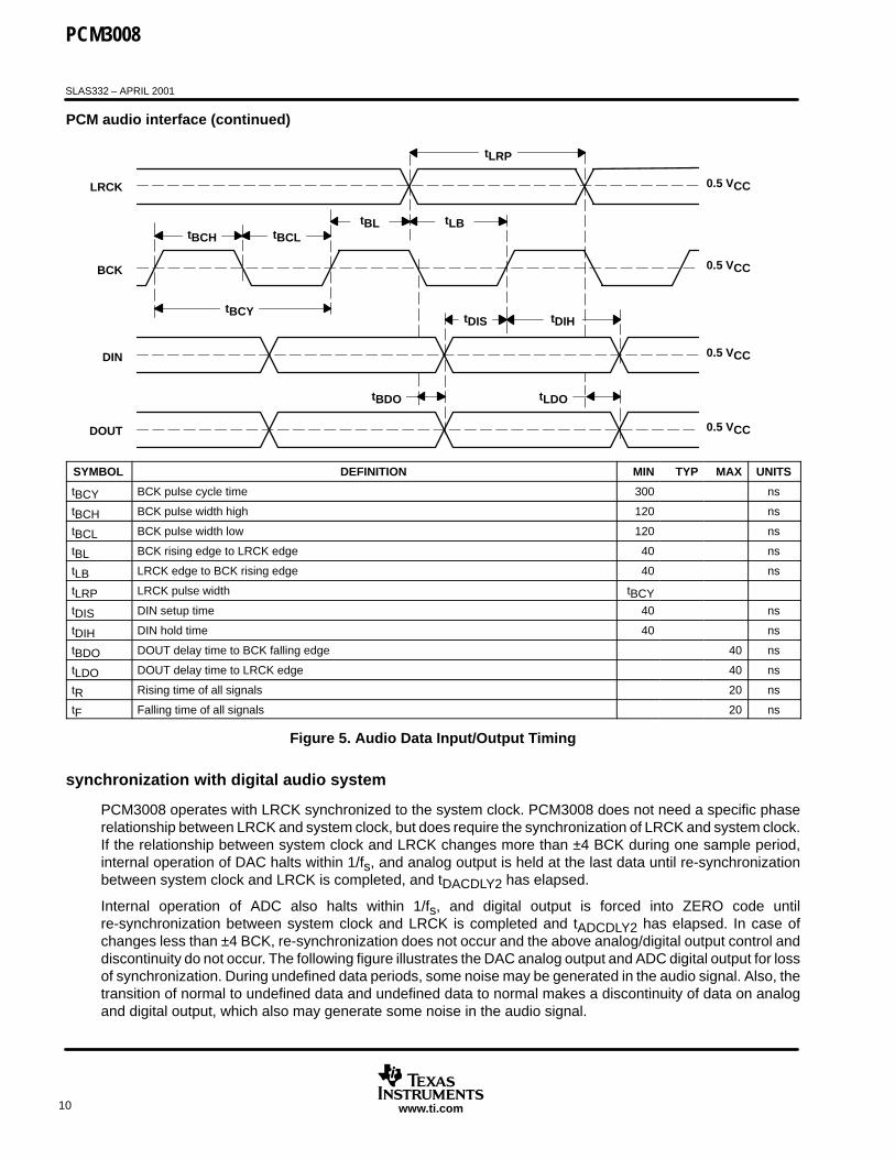
PCM audio interface
Digital audio data is interfaced to the PCM3008 on LRCK (pin 10), BCK (pin 12), DIN (pin 9), and DOUT (pin8). PCM3008 can accept 16-bit standard format, right-justified 16 bit for DAC and left-justified 16 bit for ADC.PCM3008 accepts 3 types of BCK and LRCK combination, with 64, 48 or 32 clocks of BCK in one clock of LRCK.The following figures illustrate audio data input/output format and timing.
Ready
1 1024 1025 1 1024 1025
ZERO
tRSTB1024 SYSCK 1024 SYSCK
AfterReady
AfterReady
Reset ResetResetRelease
ResetRelease
tADCDLY1 tADCDLY1
tDACDLY1 tDACDLY1tDACDLY1
VCOM (0.5 VDD)
2.1 V
0 V
VCC
SYSCK
PDAD
PDDA
InternalReset
ADCDOUT
DACVO
SYMBOL DEFINITION MIN TYP MAX UNIT
tRSTB PDAD = LOW and PDDA = LOW pulse width 40 ns
tADCDLY1 Initial delay time 2240/fs s
tDACDLY1 Fade in, fade out time 2080/fs s
Figure 3. Power-On Reset Timing
LRCK
BCK
DIN
MSB LSB MSB LSB
BCK
LRCK Right-Channel
DOUT
MSB LSB MSB LSB
16 1 2 3 14 15 16 1 2 3 14 15 16
14 15 161 2 314 15 161 2 3 1
DAC: 16-Bit, MSB-First, Right-Justified
ADC: 16-Bit, MSB-First, Left-Justified
Right-Channel
Left-Channel
Left-Channel
Figure 4. Audio Data Input/Output Format
PCM3008
SLAS332 – APRIL 2001
10 www.ti.com
PCM audio interface (continued)
0.5 VCC
0.5 VCC
0.5 VCC
0.5 VCC
tLRP
tBCH tBCLtBL tLB
tBCYtDIS tDIH
tBDO tLDO
LRCK
BCK
DIN
DOUT
SYMBOL DEFINITION MIN TYP MAX UNITS
tBCY BCK pulse cycle time 300 ns
tBCH BCK pulse width high 120 ns
tBCL BCK pulse width low 120 ns
tBL BCK rising edge to LRCK edge 40 ns
tLB LRCK edge to BCK rising edge 40 ns
tLRP LRCK pulse width tBCY
tDIS DIN setup time 40 ns
tDIH DIN hold time 40 ns
tBDO DOUT delay time to BCK falling edge 40 ns
tLDO DOUT delay time to LRCK edge 40 ns
tR Rising time of all signals 20 ns
tF Falling time of all signals 20 ns
Figure 5. Audio Data Input/Output Timing
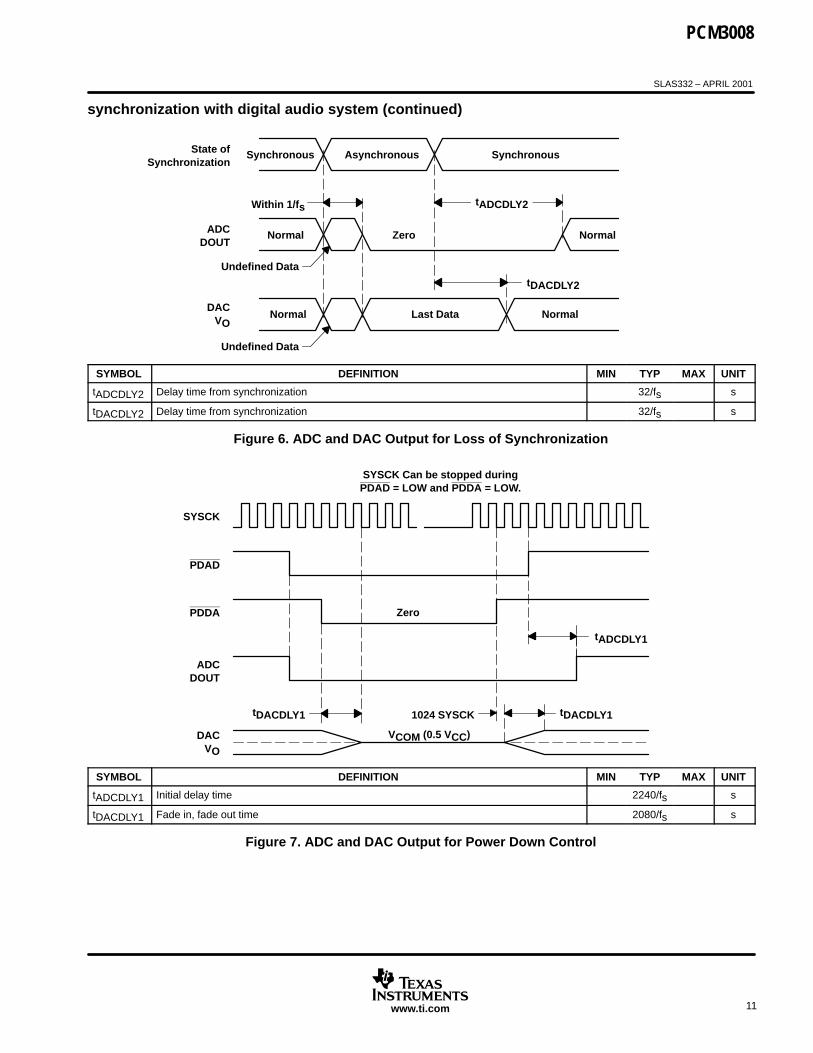
synchronization with digital audio system
PCM3008 operates with LRCK synchronized to the system clock. PCM3008 does not need a specific phaserelationship between LRCK and system clock, but does require the synchronization of LRCK and system clock.If the relationship between system clock and LRCK changes more than ±4 BCK during one sample period,internal operation of DAC halts within 1/fs, and analog output is held at the last data until re-synchronizationbetween system clock and LRCK is completed, and tDACDLY2 has elapsed.
Internal operation of ADC also halts within 1/fs, and digital output is forced into ZERO code untilre-synchronization between system clock and LRCK is completed and tADCDLY2 has elapsed. In case ofchanges less than ±4 BCK, re-synchronization does not occur and the above analog/digital output control anddiscontinuity do not occur. The following figure illustrates the DAC analog output and ADC digital output for lossof synchronization. During undefined data periods, some noise may be generated in the audio signal. Also, thetransition of normal to undefined data and undefined data to normal makes a discontinuity of data on analogand digital output, which also may generate some noise in the audio signal.
PCM3008
SLAS332 – APRIL 2001
11www.ti.com
synchronization with digital audio system (continued)
Undefined Data
Undefined Data
Within 1/fs tADCDLY2
tDACDLY2
Synchronous Asynchronous Synchronous
Normal Zero Normal
NormalNormal Last Data
State ofSynchronization
ADCDOUT
DACVO
SYMBOL DEFINITION MIN TYP MAX UNIT
tADCDLY2 Delay time from synchronization 32/fs s
tDACDLY2 Delay time from synchronization 32/fs s
Figure 6. ADC and DAC Output for Loss of Synchronization
Zero
tADCDLY1
tDACDLY11024 SYSCKtDACDLY1
VCOM (0.5 VCC)
SYSCK
PDAD
PDDA
ADCDOUT
DACVO
SYSCK Can be stopped duringPDAD = LOW and PDDA = LOW.
SYMBOL DEFINITION MIN TYP MAX UNIT
tADCDLY1 Initial delay time 2240/fs s
tDACDLY1 Fade in, fade out time 2080/fs s
Figure 7. ADC and DAC Output for Power Down Control
PCM3008
SLAS332 – APRIL 2001
12 www.ti.com
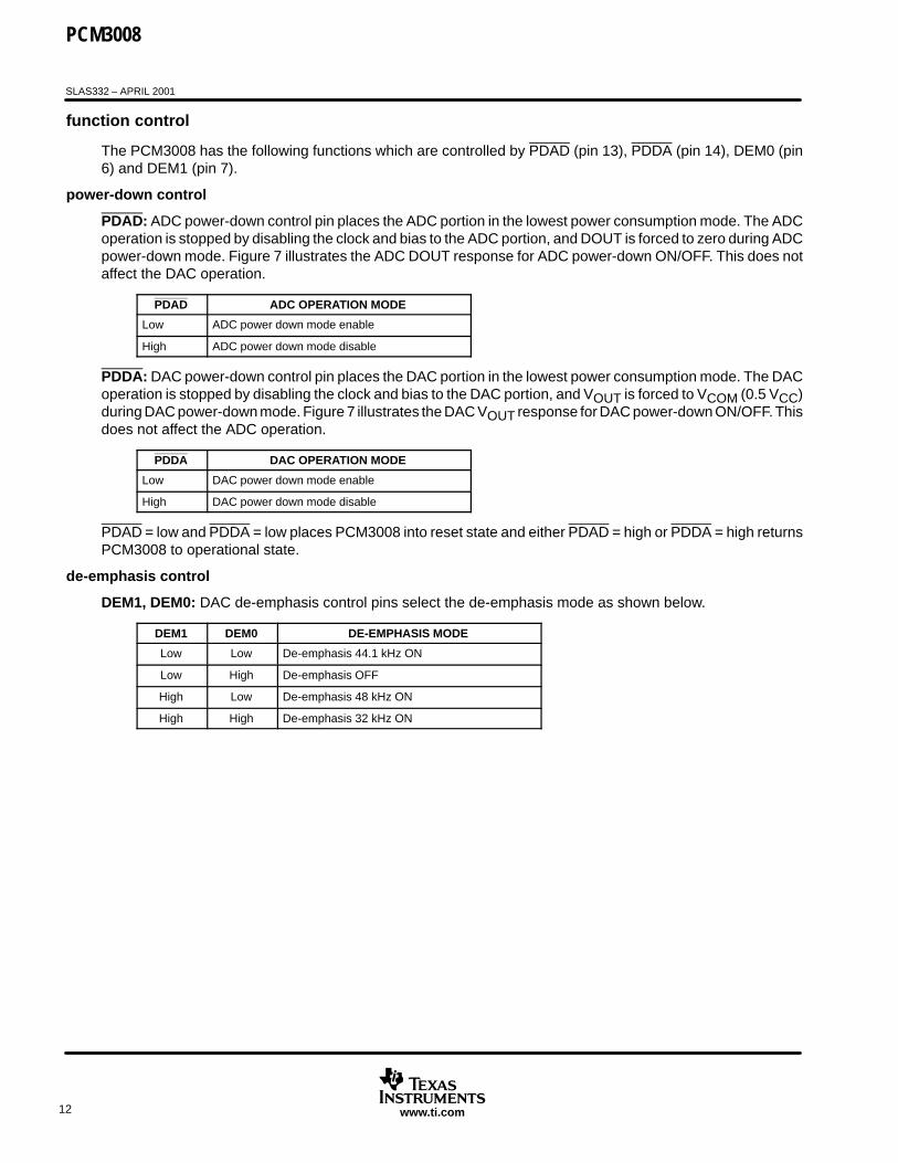
function control
The PCM3008 has the following functions which are controlled by PDAD (pin 13), PDDA (pin 14), DEM0 (pin6) and DEM1 (pin 7).
power-down control
PDAD: ADC power-down control pin places the ADC portion in the lowest power consumption mode. The ADCoperation is stopped by disabling the clock and bias to the ADC portion, and DOUT is forced to zero during ADCpower-down mode. Figure 7 illustrates the ADC DOUT response for ADC power-down ON/OFF. This does notaffect the DAC operation.
PDAD ADC OPERATION MODE
Low ADC power down mode enable
High ADC power down mode disable
PDDA: DAC power-down control pin places the DAC portion in the lowest power consumption mode. The DACoperation is stopped by disabling the clock and bias to the DAC portion, and VOUT is forced to VCOM (0.5 VCC)during DAC power-down mode. Figure 7 illustrates the DAC VOUT response for DAC power-down ON/OFF. Thisdoes not affect the ADC operation.
PDDA DAC OPERATION MODE
Low DAC power down mode enable
High DAC power down mode disable
PDAD = low and PDDA = low places PCM3008 into reset state and either PDAD = high or PDDA = high returnsPCM3008 to operational state.
de-emphasis control
DEM1, DEM0: DAC de-emphasis control pins select the de-emphasis mode as shown below.
DEM1 DEM0 DE-EMPHASIS MODE
Low Low De-emphasis 44.1 kHz ON
Low High De-emphasis OFF
High Low De-emphasis 48 kHz ON
High High De-emphasis 32 kHz ON
PCM3008
SLAS332 – APRIL 2001
13www.ti.com
TYPICAL CHARACTERISTICS
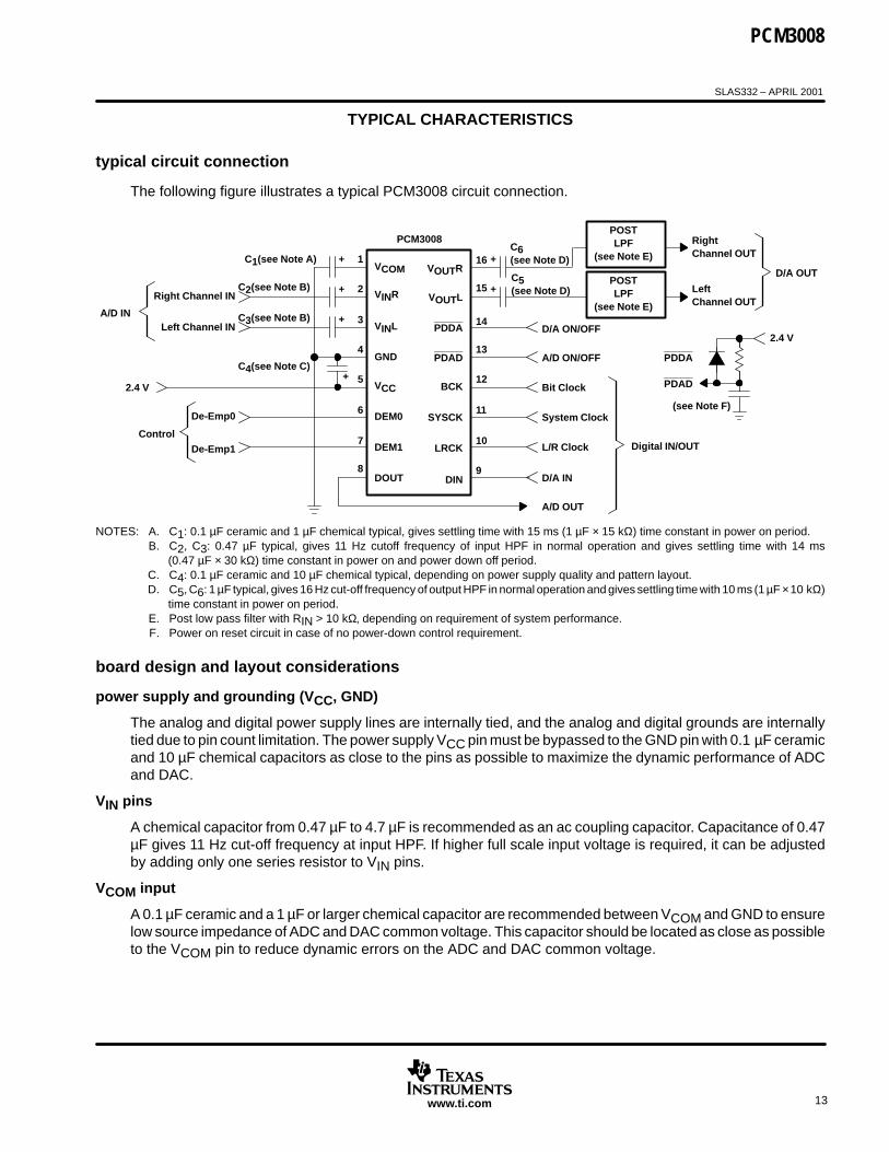
typical circuit connection
The following figure illustrates a typical PCM3008 circuit connection.
VCOM
VINR
VINL
GND
VCC
DEM0
DEM1
DOUT
VOUTR
VOUTL
PDDA
PDAD
BCK
SYSCK
LRCK
DIN
1
2
3
4
5
6
7
8 9
10
11
12
13
14
15
16+
+
+
Right Channel IN
Left Channel IN
C1(see Note A)
A/D IN
C2(see Note B)
C3(see Note B)
+C4(see Note C)
2.4 V
De-Emp0
De-Emp1
Control
+
+
C6(see Note D)
C5(see Note D)
POSTLPF
(see Note E)
POSTLPF
(see Note E)
RightChannel OUT
LeftChannel OUT
D/A OUT
D/A ON/OFF
A/D ON/OFF
Bit Clock
System Clock
L/R Clock
D/A IN
A/D OUT
Digital IN/OUT
2.4 V
PDDA
PDAD
(see Note F)
PCM3008
NOTES: A. C1: 0.1 µF ceramic and 1 µF chemical typical, gives settling time with 15 ms (1 µF × 15 kΩ) time constant in power on period.B. C2, C3: 0.47 µF typical, gives 11 Hz cutoff frequency of input HPF in normal operation and gives settling time with 14 ms
(0.47 µF × 30 kΩ) time constant in power on and power down off period.C. C4: 0.1 µF ceramic and 10 µF chemical typical, depending on power supply quality and pattern layout.D. C5, C6: 1 µF typical, gives 16 Hz cut-off frequency of output HPF in normal operation and gives settling time with 10 ms (1 µF × 10 kΩ)
time constant in power on period.E. Post low pass filter with RIN > 10 kΩ, depending on requirement of system performance.F. Power on reset circuit in case of no power-down control requirement.
board design and layout considerations
power supply and grounding (VCC, GND)
The analog and digital power supply lines are internally tied, and the analog and digital grounds are internallytied due to pin count limitation. The power supply VCC pin must be bypassed to the GND pin with 0.1 µF ceramicand 10 µF chemical capacitors as close to the pins as possible to maximize the dynamic performance of ADCand DAC.
VIN pins
A chemical capacitor from 0.47 µF to 4.7 µF is recommended as an ac coupling capacitor. Capacitance of 0.47µF gives 11 Hz cut-off frequency at input HPF. If higher full scale input voltage is required, it can be adjustedby adding only one series resistor to VIN pins.
VCOM input
A 0.1 µF ceramic and a 1 µF or larger chemical capacitor are recommended between VCOM and GND to ensurelow source impedance of ADC and DAC common voltage. This capacitor should be located as close as possibleto the VCOM pin to reduce dynamic errors on the ADC and DAC common voltage.
PCM3008
SLAS332 – APRIL 2001
14 www.ti.com
TYPICAL CHARACTERISTICS
system clock
Dynamic performance may be influenced by the quality of SYSCK. Therefore the duty cycle, jitter and thresholdvoltage at the SYSCK pin must be carefully managed. The SYSCK and BCK, LRCK must be supplied wheneverthe power is applied and either PDAD or ODDA is HIGH, as the PCM3008 uses dynamic circuits internally.
reset control
The PCM3008 does not have an internal power-on reset circuit. Therefore external reset control by PDAD andPDDA must always done at least once after the power is turned on. If neither PDAD nor PDDA is needed in theapplication, the standard reset circuit which consists of one resistor, one capacitor and one diode isrecommended on PDAD and PDDA pins.
external mute control
Although the PCM3008 has an internal muting function for power-down ON/OFF control, if external mutingcontrol is required, the recommended control sequence is described by External Mute ON, CODEC PowerDown ON, SYSCK stop and resume if necessary, CODEC Power Down OFF and External Mute OFF.
PCM3008
SLAS332 – APRIL 2001
15www.ti.com
TYPICAL CHARACTERISTICS
ADC
–88
–86
–84
–82
–80
–78
–50 –25 0 25 50 75 100
TOTAL HARMONIC DISTORTION PLUS NOISE AT –0.5 dBvs
FREE-AIR TEMPERATURE
TA – Free-Air Temperature – °CTH
D+N
– T
ota
l Har
mo
nic
Dis
tort
ion
Plu
s N
ois
e at
–0.
5 d
B –
dB
Figure 8 Figure 9
82
84
86
88
90
92
–50 –25 0 25 50 75 100
SNR
Dynamic Range
Dyn
amic
Ran
ge
An
d S
NR
– d
B
DYNAMIC RANGE AND SNRvs
FREE-AIR TEMPERATURE
TA – Free-Air Temperature – °C
–88
–86
–84
–82
–80
–78
2 2.5 3 3.5 4
TOTAL HARMONIC DISTORTION PLUS NOISE AT –0.5 dBvs
SUPPLY VOLTAGE
VCC – Supply Voltage – VTH
D+N
– T
ota
l Har
mo
nic
Dis
tort
ion
Plu
s N
ois
e at
–0.
5 d
B –
dB
Figure 10 Figure 11
82
84
86
88
90
92
2 2.5 3 3.5 4
SNR
Dynamic Range
Dyn
amic
Ran
ge
An
d S
NR
– d
B
DYNAMIC RANGE AND SNRvs
SUPPLY VOLTAGE
VCC – Supply Voltage – V
PCM3008
SLAS332 – APRIL 2001
16 www.ti.com
TYPICAL CHARACTERISTICS
ADC
–88
–86
–84
–82
–80
–78
30 35 40 45 50
TOTAL HARMONIC DISTORTION PLUS NOISE AT –0.5 dBvs
SAMPLING FREQUENCY
fs – Sampling Frequency – kHzTH
D+N
– T
ota
l Har
mo
nic
Dis
tort
ion
Plu
s N
ois
e at
–0.
5 d
B –
dB
Figure 12 Figure 13
fs – Sampling Frequency – kHz
Dyn
amic
Ran
ge
An
d S
NR
– d
B
DYNAMIC RANGE AND SNRvs
SAMPLING FREQUENCY
82
84
86
88
90
92
30 35 40 45 50
SNR
Dynamic Range
DAC
–92
–90
–88
–86
–84
–82
–50 –25 0 25 50 75 100
TOTAL HARMONIC DISTORTION PLUS NOISE AT 0 dBvs
FREE-AIR TEMPERATURE
TA – Free-Air Temperature – °CTH
D+N
– T
ota
l Har
mo
nic
Dis
tort
ion
Plu
s N
ois
e at
0 d
B –
dB
Figure 14 Figure 15
86
88
90
92
94
96
–50 –25 0 25 50 75 100
SNR
Dynamic Range
Dyn
amic
Ran
ge
An
d S
NR
– d
B
DYNAMIC RANGE AND SNRvs
FREE-AIR TEMPERATURE
TA – Free-Air Temperature – °C
PCM3008
SLAS332 – APRIL 2001
17www.ti.com
TYPICAL CHARACTERISTICS
DAC
–92
–90
–88
–86
–84
–82
2 2.5 3 3.5 4
TOTAL HARMONIC DISTORTION PLUS NOISE AT 0 dBvs
SUPPLY VOLTAGE
VCC – Supply Voltage – VTH
D+N
– T
ota
l Har
mo
nic
Dis
tort
ion
Plu
s N
ois
e at
0 d
B –
dB
Figure 16 Figure 17
86
88
90
92
94
96
2 2.5 3 3.5 4
SNR
Dynamic Range
Dyn
amic
Ran
ge
An
d S
NR
– d
B
DYNAMIC RANGE AND SNRvs
SUPPLY VOLTAGE
VCC – Supply Voltage – V
–92
–90
–88
–86
–84
–82
30 35 40 45 50
TOTAL HARMONIC DISTORTION PLUS NOISE AT 0 dBvs
SAMPLING FREQUENCY
fs – Sampling Frequency – kHz
TH
D+N
– T
ota
l Har
mo
nic
Dis
tort
ion
Plu
s N
ois
e at
0 d
B –
dB
Figure 18 Figure 19
86
88
90
92
94
96
30 35 40 45 50fs – Sampling Frequency – kHz
Dyn
amic
Ran
ge
An
d S
NR
– d
B
DYNAMIC RANGE AND SNRvs
SAMPLING FREQUENCY
SNR
Dynamic Range

PCM3008
SLAS332 – APRIL 2001
18 www.ti.com
TYPICAL CHARACTERISTICS
–140
–120
–100
–80
–60
–40
–20
0
0 5 10 15 20
Am
plit
ud
e –
dB
f – Frequency – kHz
OUTPUT SPECTRUM
–0.5 dB,N = 8192
Figure 20 Figure 21
ADC DAC
–140
–120
–100
–80
–60
–40
–20
0
0 5 10 15 20
Am
plit
ud
e –
dB
f – Frequency – kHz
OUTPUT SPECTRUM
0 dB,N = 8192
–140
–120
–100
–80
–60
–40
–20
0
0 5 10 15 20
Am
plit
ud
e –
dB
f – Frequency – kHz
OUTPUT SPECTRUM
–60 dB,N = 8192
Figure 22 Figure 23
–140
–120
–100
–80
–60
–40
–20
0
0 5 10 15 20
Am
plit
ud
e –
dB
f – Frequency – kHz
OUTPUT SPECTRUM
–60 dB,N = 8192
PCM3008
SLAS332 – APRIL 2001
19www.ti.com
TYPICAL CHARACTERISTICS
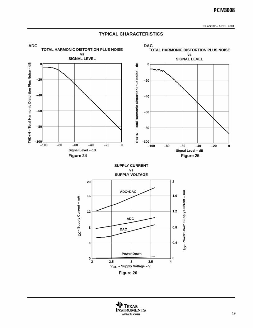
Figure 24 Figure 25
ADC DAC
–100
–80
–60
–40
–20
0
–100 –80 –60 –40 –20 0
TOTAL HARMONIC DISTORTION PLUS NOISEvs
SIGNAL LEVEL
Signal Level – dB
TH
D+N
– T
ota
l Har
mo
nic
Dis
tort
ion
Plu
s N
ois
e –
dB
–100
–80
–60
–40
–20
0
–100 –80 –60 –40 –20 0
TOTAL HARMONIC DISTORTION PLUS NOISEvs
SIGNAL LEVEL
Signal Level – dB
TH
D+N
– T
ota
l Har
mo
nic
Dis
tort
ion
Plu
s N
ois
e –
dB
Figure 26
0
4
8
12
16
20
2 2.5 3 3.5 40
0.4
0.8
1.2
1.6
2
ADC+DAC
ADC
DAC
Power Down
SUPPLY CURRENTvs
SUPPLY VOLTAGE
VCC – Supply Voltage – V
– S
up
ply
Cu
rren
t –
mA
I CC
– P
ow
er D
ow
n S
up
ply
Cu
rren
t –
mA
I D
PCM3008
SLAS332 – APRIL 2001
20 www.ti.com
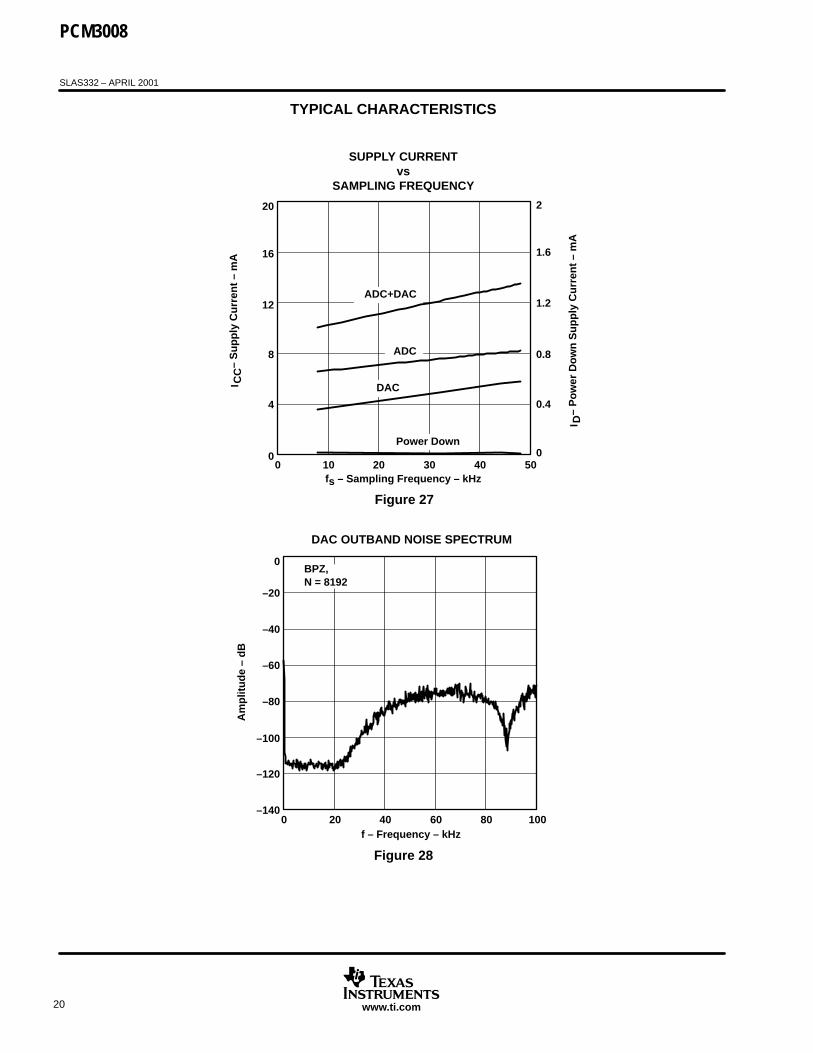
TYPICAL CHARACTERISTICS
0
4
8
12
16
20
0 10 20 30 40 500
0.4
0.8
1.2
1.6
2
ADC+DAC
ADC
DAC
Power Down
SUPPLY CURRENTvs
SAMPLING FREQUENCY
– S
up
ply
Cu
rren
t –
mA
I CC
– P
ow
er D
ow
n S
up
ply
Cu
rren
t –
mA
I D
fs – Sampling Frequency – kHz
Figure 27
–140
–120
–100
–80
–60
–40
–20
0
0 20 40 60 80 100
Am
plit
ud
e –
dB
f – Frequency – kHz
DAC OUTBAND NOISE SPECTRUM
BPZ,N = 8192
Figure 28
PCM3008
SLAS332 – APRIL 2001
21www.ti.com
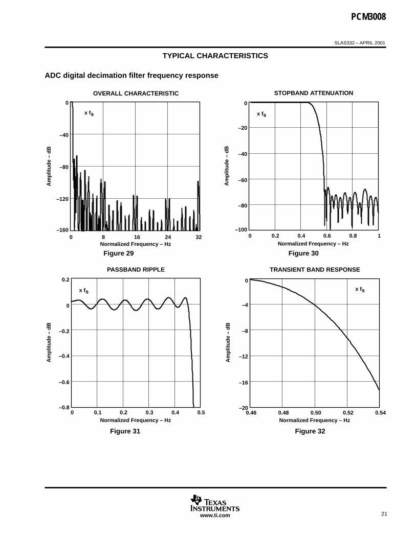
TYPICAL CHARACTERISTICS
ADC digital decimation filter frequency response
–160
–120
–80
–40
0
0 8 16 24 32
Am
plit
ud
e –
dB
Normalized Frequency – Hz
OVERALL CHARACTERISTIC
x fs
Figure 29 Figure 30
–100
–80
–60
–40
–20
0
0 0.2 0.4 0.6 0.8 1
Am
plit
ud
e –
dB
Normalized Frequency – Hz
STOPBAND ATTENUATION
x fs
–0.8
–0.6
–0.4
–0.2
0
0.2
0 0.1 0.2 0.3 0.4 0.5
Am
plit
ud
e –
dB
Normalized Frequency – Hz
PASSBAND RIPPLE
x fs
–20
–16
–12
–8
–4
0
0.46 0.48 0.50 0.52 0.54
Am
plit
ud
e –
dB
Normalized Frequency – Hz
TRANSIENT BAND RESPONSE
x fs
Figure 31 Figure 32

PCM3008
SLAS332 – APRIL 2001
22 www.ti.com
TYPICAL CHARACTERISTICS
digital high pass filter frequency response
–100
–80
–60
–40
–20
0
0 0.1 0.2 0.3 0.4
Am
plit
ud
e –
dB
Normalized Frequency – Hz
STOPBAND CHARACTERISTIC
x fs/1000
Figure 33 Figure 34
–1
–0.8
–0.6
–0.4
–0.2
0
0 1 2 3 4
Am
plit
ud
e –
dB
Normalized Frequency – Hz
PASSBAND CHARACTERISTIC
x fs/1000
analog antialiasing filter frequency response
–50
–40
–30
–20
–10
0
1 10 100 1 k 10 k
Am
plit
ud
e –
dB
f – Frequency – kHz
STOPBAND CHARACTERISTIC
Figure 35 Figure 36
–1
–0.8
–0.6
–0.4
–0.2
0
0.01 0.1 1 10 100
Am
plit
ud
e –
dB
PASSBAND CHARACTERISTIC
f – Frequency – kHz
PCM3008
SLAS332 – APRIL 2001
23www.ti.com
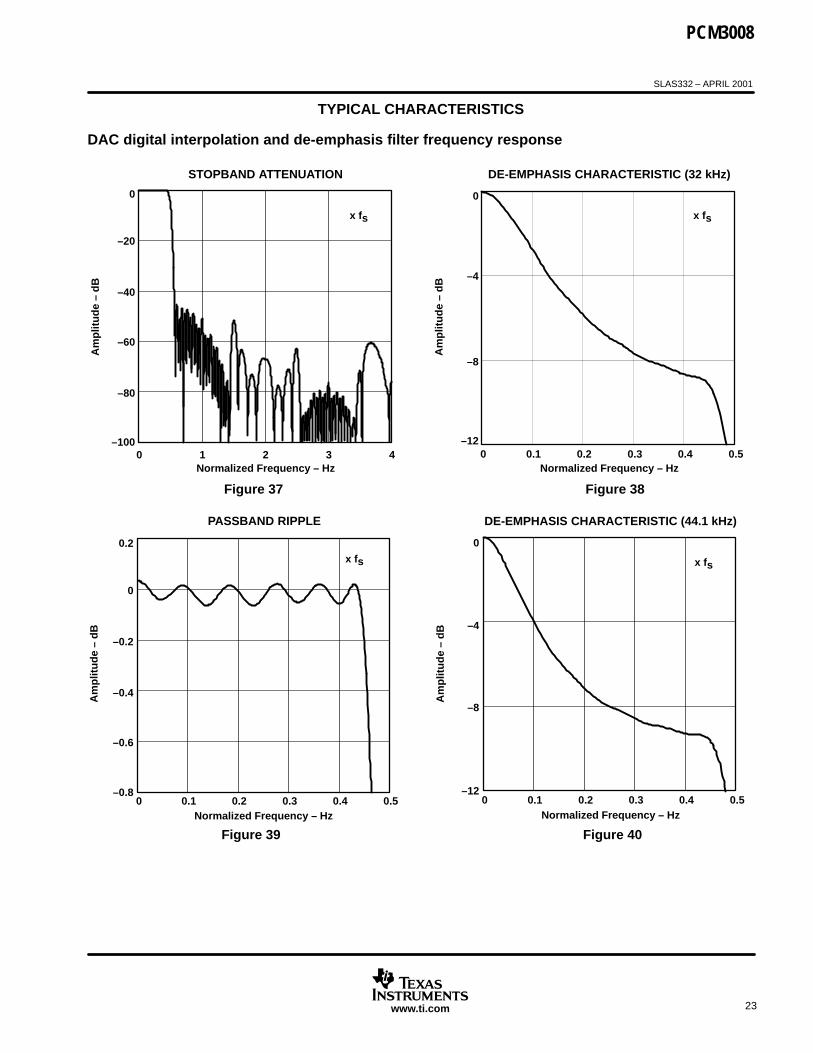
TYPICAL CHARACTERISTICS
DAC digital interpolation and de-emphasis filter frequency response
–100
–80
–60
–40
–20
0
0 1 2 3 4
Am
plit
ud
e –
dB
STOPBAND ATTENUATION
Normalized Frequency – Hz
x fs
Figure 37 Figure 38
–12
–8
–4
0
0 0.1 0.2 0.3 0.4 0.5A
mp
litu
de
– d
B
DE-EMPHASIS CHARACTERISTIC (32 kHz)
Normalized Frequency – Hz
x fs
–0.8
–0.6
–0.4
–0.2
0
0.2
0 0.1 0.2 0.3 0.4 0.5
Am
plit
ud
e –
dB
Normalized Frequency – Hz
PASSBAND RIPPLE
x fs
Figure 39 Figure 40
–12
–8
–4
0
0 0.1 0.2 0.3 0.4 0.5
Am
plit
ud
e –
dB
DE-EMPHASIS CHARACTERISTIC (44.1 kHz)
Normalized Frequency – Hz
x fs
PCM3008
SLAS332 – APRIL 2001
24 www.ti.com
TYPICAL CHARACTERISTICS
DAC digital interpolation and de-emphasis filter frequency response (continued)
–20
–16
–12
–8
–4
0
0.46 0.48 0.50 0.52 0.54
Am
plit
ud
e –
dB
TRANSIENT BAND RESPONSE
Normalized Frequency – Hz
x fs
Figure 41 Figure 42
–12
–8
–4
0
0 0.1 0.2 0.3 0.4 0.5
Am
plit
ud
e –
dB
DE-EMPHASIS CHARACTERISTIC (48 kHz)
Normalized Frequency – Hz
x fs
analog FIR filter frequency response
–50
–40
–30
–20
–10
0
0 8 16 24 32
Am
plit
ud
e –
dB
STOPBAND CHARACTERISTIC
Normalized Frequency – Hz
x fs
Figure 43 Figure 44
–0.8
–0.6
–0.4
–0.2
0
0.2
0 0.1 0.2 0.3 0.4 0.5
Am
plit
ud
e –
dB
PASSBAND CHARACTERISTIC
Normalized Frequency – Hz
x fs
PCM3008
SLAS332 – APRIL 2001
25www.ti.com
TYPICAL CHARACTERISTICS
analog low pass filter frequency response
Figure 45 Figure 46
–50
–40
–30
–20
–10
0
1 10 100 1 k 10 k
Am
plit
ud
e –
dB
STOPBAND CHARACTERISTIC
f – Frequency – kHz
–1
–0.8
–0.6
–0.4
–0.2
0
0.01 0.1 1 10 100A
mp
litu
de
– d
B
PASSBAND CHARACTERISTIC
f – Frequency – kHz
®
PACKAGE DRAWINGS
MPDS090
PACKAGING INFORMATION
Orderable Device Status (1) PackageType
PackageDrawing
Pins PackageQty
Eco Plan (2) Lead/Ball Finish MSL Peak Temp (3)
PCM3008T ACTIVE TSSOP PW 16 90 Green (RoHS &no Sb/Br)
CU NIPDAU Level-1-260C-UNLIM
PCM3008T/2K ACTIVE TSSOP PW 16 2000 Green (RoHS &no Sb/Br)
CU NIPDAU Level-1-260C-UNLIM
PCM3008T/2KG4 ACTIVE TSSOP PW 16 2000 Green (RoHS &no Sb/Br)
CU NIPDAU Level-1-260C-UNLIM
PCM3008TG4 ACTIVE TSSOP PW 16 90 Green (RoHS &no Sb/Br)
CU NIPDAU Level-1-260C-UNLIM
(1) The marketing status values are defined as follows:ACTIVE: Product device recommended for new designs.LIFEBUY: TI has announced that the device will be discontinued, and a lifetime-buy period is in effect.NRND: Not recommended for new designs. Device is in production to support existing customers, but TI does not recommend using this part ina new design.PREVIEW: Device has been announced but is not in production. Samples may or may not be available.OBSOLETE: TI has discontinued the production of the device.
(2) Eco Plan - The planned eco-friendly classification: Pb-Free (RoHS), Pb-Free (RoHS Exempt), or Green (RoHS & no Sb/Br) - please checkhttp://www.ti.com/productcontent for the latest availability information and additional product content details.TBD: The Pb-Free/Green conversion plan has not been defined.Pb-Free (RoHS): TI's terms "Lead-Free" or "Pb-Free" mean semiconductor products that are compatible with the current RoHS requirementsfor all 6 substances, including the requirement that lead not exceed 0.1% by weight in homogeneous materials. Where designed to be solderedat high temperatures, TI Pb-Free products are suitable for use in specified lead-free processes.Pb-Free (RoHS Exempt): This component has a RoHS exemption for either 1) lead-based flip-chip solder bumps used between the die andpackage, or 2) lead-based die adhesive used between the die and leadframe. The component is otherwise considered Pb-Free (RoHScompatible) as defined above.Green (RoHS & no Sb/Br): TI defines "Green" to mean Pb-Free (RoHS compatible), and free of Bromine (Br) and Antimony (Sb) based flameretardants (Br or Sb do not exceed 0.1% by weight in homogeneous material)
(3) MSL, Peak Temp. -- The Moisture Sensitivity Level rating according to the JEDEC industry standard classifications, and peak soldertemperature.
Important Information and Disclaimer:The information provided on this page represents TI's knowledge and belief as of the date that it isprovided. TI bases its knowledge and belief on information provided by third parties, and makes no representation or warranty as to theaccuracy of such information. Efforts are underway to better integrate information from third parties. TI has taken and continues to takereasonable steps to provide representative and accurate information but may not have conducted destructive testing or chemical analysis onincoming materials and chemicals. TI and TI suppliers consider certain information to be proprietary, and thus CAS numbers and other limitedinformation may not be available for release.
In no event shall TI's liability arising out of such information exceed the total purchase price of the TI part(s) at issue in this document sold by TIto Customer on an annual basis.
PACKAGE OPTION ADDENDUM
www.ti.com 12-Mar-2008
Addendum-Page 1
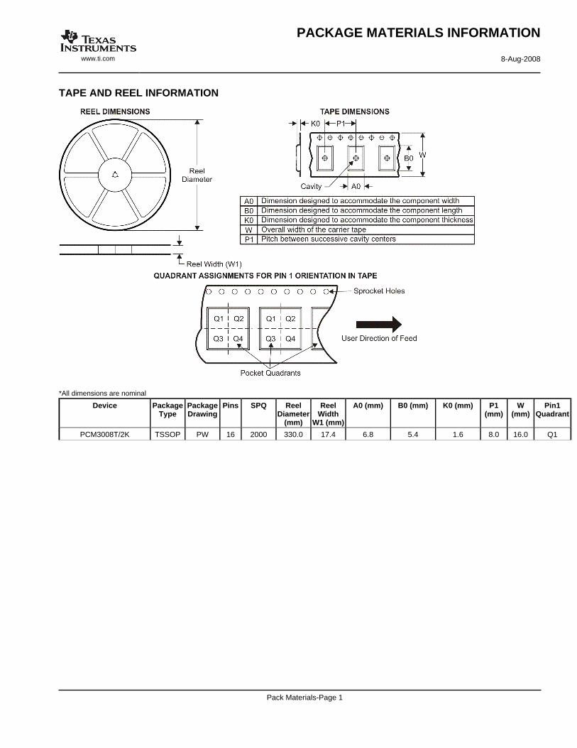
TAPE AND REEL INFORMATION
*All dimensions are nominal
Device PackageType
PackageDrawing
Pins SPQ ReelDiameter
(mm)
ReelWidth
W1 (mm)
A0 (mm) B0 (mm) K0 (mm) P1(mm)
W(mm)
Pin1Quadrant
PCM3008T/2K TSSOP PW 16 2000 330.0 17.4 6.8 5.4 1.6 8.0 16.0 Q1
PACKAGE MATERIALS INFORMATION
www.ti.com 8-Aug-2008
Pack Materials-Page 1
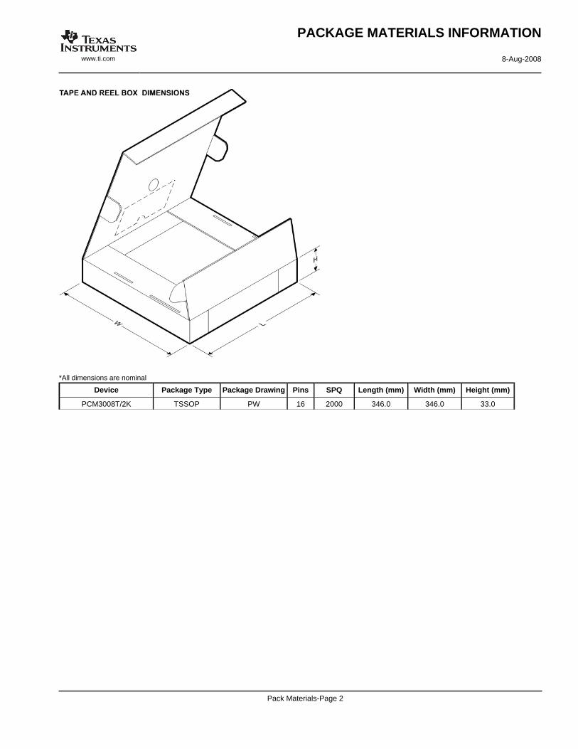
*All dimensions are nominal
Device Package Type Package Drawing Pins SPQ Length (mm) Width (mm) Height (mm)
PCM3008T/2K TSSOP PW 16 2000 346.0 346.0 33.0
PACKAGE MATERIALS INFORMATION
www.ti.com 8-Aug-2008
Pack Materials-Page 2
IMPORTANT NOTICETexas Instruments Incorporated and its subsidiaries (TI) reserve the right to make corrections, modifications, enhancements, improvements,and other changes to its products and services at any time and to discontinue any product or service without notice. Customers shouldobtain the latest relevant information before placing orders and should verify that such information is current and complete. All products aresold subject to TI’s terms and conditions of sale supplied at the time of order acknowledgment.TI warrants performance of its hardware products to the specifications applicable at the time of sale in accordance with TI’s standardwarranty. Testing and other quality control techniques are used to the extent TI deems necessary to support this warranty. Except wheremandated by government requirements, testing of all parameters of each product is not necessarily performed.TI assumes no liability for applications assistance or customer product design. Customers are responsible for their products andapplications using TI components. To minimize the risks associated with customer products and applications, customers should provideadequate design and operating safeguards.TI does not warrant or represent that any license, either express or implied, is granted under any TI patent right, copyright, mask work right,or other TI intellectual property right relating to any combination, machine, or process in which TI products or services are used. Informationpublished by TI regarding third-party products or services does not constitute a license from TI to use such products or services or awarranty or endorsement thereof. Use of such information may require a license from a third party under the patents or other intellectualproperty of the third party, or a license from TI under the patents or other intellectual property of TI.Reproduction of TI information in TI data books or data sheets is permissible only if reproduction is without alteration and is accompaniedby all associated warranties, conditions, limitations, and notices. Reproduction of this information with alteration is an unfair and deceptivebusiness practice. TI is not responsible or liable for such altered documentation. Information of third parties may be subject to additionalrestrictions.Resale of TI products or services with statements different from or beyond the parameters stated by TI for that product or service voids allexpress and any implied warranties for the associated TI product or service and is an unfair and deceptive business practice. TI is notresponsible or liable for any such statements.TI products are not authorized for use in safety-critical applications (such as life support) where a failure of the TI product would reasonablybe expected to cause severe personal injury or death, unless officers of the parties have executed an agreement specifically governingsuch use. Buyers represent that they have all necessary expertise in the safety and regulatory ramifications of their applications, andacknowledge and agree that they are solely responsible for all legal, regulatory and safety-related requirements concerning their productsand any use of TI products in such safety-critical applications, notwithstanding any applications-related information or support that may beprovided by TI. Further, Buyers must fully indemnify TI and its representatives against any damages arising out of the use of TI products insuch safety-critical applications.TI products are neither designed nor intended for use in military/aerospace applications or environments unless the TI products arespecifically designated by TI as military-grade or "enhanced plastic." Only products designated by TI as military-grade meet militaryspecifications. Buyers acknowledge and agree that any such use of TI products which TI has not designated as military-grade is solely atthe Buyer's risk, and that they are solely responsible for compliance with all legal and regulatory requirements in connection with such use.TI products are neither designed nor intended for use in automotive applications or environments unless the specific TI products aredesignated by TI as compliant with ISO/TS 16949 requirements. Buyers acknowledge and agree that, if they use any non-designatedproducts in automotive applications, TI will not be responsible for any failure to meet such requirements.Following are URLs where you can obtain information on other Texas Instruments products and application solutions:Products ApplicationsAmplifiers amplifier.ti.com Audio www.ti.com/audioData Converters dataconverter.ti.com Automotive www.ti.com/automotiveDSP dsp.ti.com Broadband www.ti.com/broadbandClocks and Timers www.ti.com/clocks Digital Control www.ti.com/digitalcontrolInterface interface.ti.com Medical www.ti.com/medicalLogic logic.ti.com Military www.ti.com/militaryPower Mgmt power.ti.com Optical Networking www.ti.com/opticalnetworkMicrocontrollers microcontroller.ti.com Security www.ti.com/securityRFID www.ti-rfid.com Telephony www.ti.com/telephonyRF/IF and ZigBee® Solutions www.ti.com/lprf Video & Imaging www.ti.com/video
Wireless www.ti.com/wireless
Mailing Address: Texas Instruments, Post Office Box 655303, Dallas, Texas 75265Copyright © 2008, Texas Instruments Incorporated