Embed Size (px)
Citation preview

LTC1852/LTC1853
118523fa
BLOCK DIAGRAM
FEATURES
APPLICATIONS
DESCRIPTION
8-Channel, 10-Bit/12-Bit, 400ksps, Low Power, Sampling ADCs
The 10-bit LTC®1852 and 12-bit LTC1853 are complete 8-channel data acquisition systems. They include a fl exible 8-channel multiplexer, a 400ksps successive approxima-tion analog-to-digital converter, an internal reference and a parallel output interface. The multiplexer can be confi gured for single-ended or differential inputs, two gain ranges and unipolar or bipolar operation. The ADCs have a scan mode that will repeatedly cycle through all 8 multiplexer channels and can also be programmed to sequence through up to 16 addresses and confi gurations. The sequence can also be read back from internal memory.
The reference and buffer amplifi er provide pin strappable ranges of 4.096V, 2.5V and 2.048V. The parallel output includes the 10-bit or 12-bit conversion result plus the 4-bit multiplexer address. The digital outputs are pow-ered from a separate supply allowing for easy interface to 3V digital logic. Typical power consumption is 10mW at 400ksps from a single 5V supply and 3mW at 250ksps from a single 3V supply.
n Flexible 8-Channel Multiplexer Single-Ended or Differential Inputs Two Gain Ranges Unipolar or Bipolar Operationn Scan Mode and Programmable Sequencer
Eliminate Confi guration Software Overheadn Low Power: 3mW at 250kspsn 2.7V to 5.5V Supply Rangen Internal or External Reference Operationn Parallel Output Includes MUX Address n Nap and Sleep Shutdown Modesn Pin Compatible up-grade 1.25Msps 10-Bit LTC1850
and 12-Bit LTC1851
n High Speed Data Acquisitionn Test and Measurementn Imaging Systemsn Telecommunicationsn Industrial Process Controln Spectrum Analysis
BUSYDIFFOUT/S6A2OUT/S5A1OUT/S4A0OUT/S3D11/S2D10/S1D9/S0D8D7D6D5D4D3D2D1D0
M1SHDNCSCONVSTRDWRDIFFA2A1A0UNI/BIPPGAM0
OUTPUTDRIVERS
DATALATCHES
OGND18523 BD
OVDD
REF AMP
REFCOMP
REFIN
REFOUT
COM
CH7
CH6
CH5
CH4
CH3
CH2
CH1
CH0
8-CHANNELMULTIPLEXER
2.5VREFERENCE
INTERNALCLOCK
LTC1853
CONTROL LOGICAND
PROGRAMMABLESEQUENCER
12-BITSAMPLING
ADC
+–
Integral Linearity
0 512 1024 1536 2048 2560 3072 3584 4096
CODE
1.0
0.5
0
–0.5
–1.0
INL
ER
RO
R (
LS
Bs)
1852 F01
, LT, LTC and LTM are registered trademarks of Linear Technology Corporation.
LTC1852/LTC1853
218523fa
PIN CONFIGURATION
ABSOLUTE MAXIMUM RATINGS OVDD = VDD (Note 1, 2)
ORDER INFORMATION
Supply Voltage (VDD) ..................................................6VAnalog Input Voltage (Note 3) ..... –0.3V to (VDD + 0.3V)Digital Input Voltage (Note 4) .................... –0.3V to 10VDigital Output Voltage ..................–0.3V to (VDD + 0.3V)Power Dissipation ...............................................500mW
Ambient Operating Temperature Range LTC1852C/LTC1853C .............................. 0°C to 70°C LTC1852I/LTC1853I ............................. –40°C to 85°CStorage Temperature Range ...................–65°C to 150°CLead Temperature (Soldering, 10 sec) ................. 300°C
LEAD FREE FINISH TAPE AND REEL PART MARKING PACKAGE DESCRIPTION TEMPERATURE RANGE
LTC1852CFW#PBF LTC1852CFW#TRPBF LTC1852CFW 48-Lead Plastic TSSOP (6.1mm) 0°C to 70°C
LTC1852IFW#PBF LTC1852IFW#TRPBF LTC1852IFW 48-Lead Plastic TSSOP (6.1mm) –40°C to 85°C
LTC1853CFW#PBF LTC1853CFW#TRPBF LTC1853CFW 48-Lead Plastic TSSOP (6.1mm) 0°C to 70°C
LTC1853IFW#PBF LTC1853IFW#TRPBF LTC1853IFW 48-Lead Plastic TSSOP (6.1mm) –40°C to 85°C
Consult LTC Marketing for parts specifi ed with wider operating temperature ranges.
Consult LTC Marketing for information on non-standard lead based fi nish parts.
For more information on lead free part marking, go to: http://www.linear.com/leadfree/ For more information on tape and reel specifi cations, go to: http://www.linear.com/tapeandreel/
LTC1852
1
2
3
4
5
6
7
8
9
10
11
12
13
14
15
16
17
18
19
20
21
22
23
24
TOP VIEW
FW PACKAGE48-LEAD PLASTIC TSSOP
48
47
46
45
44
43
42
41
40
39
38
37
36
35
34
33
32
31
30
29
28
27
26
25
CH0
CH1
CH2
CH3
CH4
CH5
CH6
CH7
COM
REFOUT
REFIN
REFCOMP
GND
VDD
VDD
GND
DIFFOUT/S6
A2OUT/S5
A1OUT/S4
A0OUT/S3
D9/S2
D8/S1
D7/S0
D6
M1
SHDN
CS
CONVST
RD
WR
DIFF
A2
A1
A0
UNI/BIP
PGA
M0
OVDD
OGND
BUSY
NC
NC
D0
D1
D2
D3
D4
D5
LTC1853
1
2
3
4
5
6
7
8
9
10
11
12
13
14
15
16
17
18
19
20
21
22
23
24
TOP VIEW
FW PACKAGE48-LEAD PLASTIC TSSOP
48
47
46
45
44
43
42
41
40
39
38
37
36
35
34
33
32
31
30
29
28
27
26
25
CH0
CH1
CH2
CH3
CH4
CH5
CH6
CH7
COM
REFOUT
REFIN
REFCOMP
GND
VDD
VDD
GND
DIFFOUT/S6
A2OUT/S5
A1OUT/S4
A0OUT/S3
D11/S2
D10/S1
D9/S0
D8
M1
SHDN
CS
CONVST
RD
WR
DIFF
A2
A1
A0
UNI/BIP
PGA
M0
OVDD
OGND
BUSY
D0
D1
D2
D3
D4
D5
D6
D7
TJMAX = 150°C, θJA = 110°C/W TJMAX = 150°C, θJA = 110°C/W

LTC1852/LTC1853
318523fa
CONVERTER CHARACTERISTICS The l denotes the specifi cations which apply over the full operating temperature range, otherwise specifi cations are at TA = 25°C. VDD = 2.7V to 5.5V, REFCOMP < VDD (Notes 5,6)
PARAMETER CONDITIONS MINLTC1852
TYP MAX MINLTC1853
TYP MAX UNITS
Resolution (No Missing Codes) l 10 12 Bits
Integral Linearity Error (Note 7) l ±0.25 ±1 ±0.35 ±1 LSB
Differential Linearity Error l ±0.25 ±1 ±0.25 ±1 LSB
Offset Error (Bipolar and Unipolar)Gain = 1 (PGA = 1)Gain = 2 (PGA = 0)
(Note 8)REFCOMP ≥ 2V l
l
±0.5±1
±2±4
±1±2
±6±12
LSBLSB
Offset Error Match (Bipolar and Unipolar) ±0.5 ±1 LSB
Unipolar Gain ErrorGain = 1 (PGA = 1)Gain = 2 (PGA = 0)
With External 4.096V ReferenceApplied to REFCOMP (Note 12)VDD = 4.75V to 5.25V, fS ≤ 400kHz
±2±4
±4±8
LSBLSB
Unipolar Gain Error Match ±0.5 ±1 LSB
Bipolar Gain ErrorGain = 1 (PGA = 1)Gain = 2 (PGA = 0)
With External 4.096V ReferenceApplied to REFCOMP (Note 12)VDD = 4.75V to 5.25V, fS ≤ 400kHz
±2±4
±4±8
LSBLSB
Bipolar Gain Error Match ±0.5 ±1 LSB
Unipolar Gain ErrorGain = 1 (PGA = 1)Gain = 2 (PGA = 0)
With External 2.5V ReferenceApplied to REFCOMPVDD = 2.7V to 5.5V, fS ≤ 250kHz
l
l
±1±2
±3±6
±1.5±3
±8±16
LSBLSB
Bipolar Gain ErrorGain = 1 (PGA = 1)Gain = 2 (PGA = 0)
With External 2.5V ReferenceApplied to REFCOMPVDD = 2.7V to 5.5V, fS ≤ 250kHz
l
l
±1±2
±3±6
±1.5±3
±8±16
LSBLSB
Full-Scale Error Temperature Coeffi cient 15 15 ppm/°C
SYMBOL PARAMETER CONDITIONS MIN TYP MAX UNITS
VIN Analog Input Range (Note 9)Unipolar, Gain = 1 (PGA = 1)Unipolar, Gain = 2 (PGA = 0)Bipolar, Gain = 1 (PGA = 1)Bipolar, Gain = 2 (PGA = 0)
2.7V ≤ VDD ≤ 5.5V, REFCOMP ≤ VDD0 – REFCOMP0 – REFCOMP/2±REFCOMP/2±REFCOMP/4
VVVV
IIN Analog Input Leakage Current l ±1 μA
CIN Analog Input Capacitance Between Conversions (Gain = 1)Between Conversions (Gain = 2)During Conversions
15255
pFpFpF
tACQ Sample-and-Hold Acquisition Time 50 150 ns
tS(MUX) Multiplexer Settling Time (Includes tACQ) 50 150 ns
tAP Sample-and-Hold Aperture Delay Time VDD = 5V –0.5 ns
tjitter Sample-and-Hold Aperture Delay Time Jitter VDD = 5V 2 psRMS
CMRR Analog Input Common Mode Rejection Ratio 60 dB
ANALOG INPUT The l denotes the specifi cations which apply over the full operating temperature range, otherwise specifi cations are at TA = 25°C. (Notes 5)
DYNAMIC ACCURACY TA = 25°C. (Notes 5)
SYMBOL PARAMETER CONDITIONS MIN TYP MAX UNITS
S/(N + D) Signal-to-Noise Plus Distortion Ratio 40kHz Input Signal 72.5 dB
THD Total Harmonic Distortion 40kHz Input Signal, First 5 Harmonics –80 dB
SFDR Spurious Free Dynamic Range 40kHz Input Signal –85 dB
LTC1852/LTC1853
418523fa
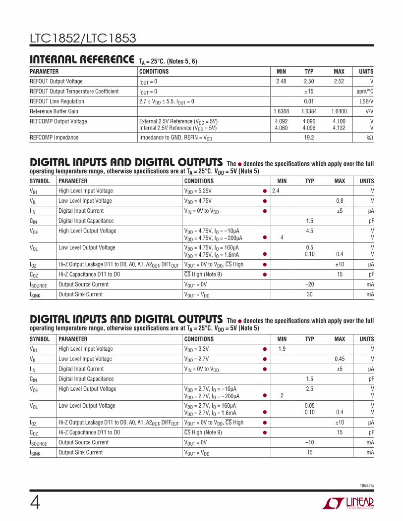
INTERNAL REFERENCE TA = 25°C. (Notes 5, 6)
PARAMETER CONDITIONS MIN TYP MAX UNITS
REFOUT Output Voltage IOUT = 0 2.48 2.50 2.52 V
REFOUT Output Temperature Coeffi cient IOUT = 0 ±15 ppm/°C
REFOUT Line Regulation 2.7 ≤ VDD ≤ 5.5, IOUT = 0 0.01 LSB/V
Reference Buffer Gain 1.6368 1.6384 1.6400 V/V
REFCOMP Output Voltage External 2.5V Reference (VDD = 5V)Internal 2.5V Reference (VDD = 5V)
4.0924.060
4.0964.096
4.1004.132
VV
REFCOMP Impedance Impedance to GND, REFIN = VDD 19.2 kΩ
SYMBOL PARAMETER CONDITIONS MIN TYP MAX UNITS
VIH High Level Input Voltage VDD = 5.25V ● 2.4 V
VIL Low Level Input Voltage VDD = 4.75V ● 0.8 V
IIN Digital Input Current VIN = 0V to VDD ● ±5 μA
CIN Digital Input Capacitance 1.5 pF
VOH High Level Output Voltage VDD = 4.75V, IO = –10μA
VDD = 4.75V, IO = –200μA ● 44.5 V
V
VOL Low Level Output Voltage VDD = 4.75V, IO = 160μA
VDD = 4.75V, IO = 1.6mA ●0.5
0.10 0.4VV
IOZ Hi-Z Output Leakage D11 to D0, A0, A1, A2OUT, DIFFOUT VOUT = 0V to VDD, CS High ● ±10 μA
COZ Hi-Z Capacitance D11 to D0 CS High (Note 9) ● 15 pF
ISOURCE Output Source Current VOUT = 0V –20 mA
ISINK Output Sink Current VOUT = VDD 30 mA
DIGITAL INPUTS AND DIGITAL OUTPUTS The ● denotes the specifi cations which apply over the full operating temperature range, otherwise specifi cations are at TA = 25°C. VDD = 5V (Note 5)
DIGITAL INPUTS AND DIGITAL OUTPUTS The ● denotes the specifi cations which apply over the full operating temperature range, otherwise specifi cations are at TA = 25°C. VDD = 5V (Note 5)
SYMBOL PARAMETER CONDITIONS MIN TYP MAX UNITS
VIH High Level Input Voltage VDD = 3.3V ● 1.9 V
VIL Low Level Input Voltage VDD = 2.7V ● 0.45 V
IIN Digital Input Current VIN = 0V to VDD ● ±5 μA
CIN Digital Input Capacitance 1.5 pF
VOH High Level Output Voltage VDD = 2.7V, IO = –10μA
VDD = 2.7V, IO = –200μA ● 22.5 V
V
VOL Low Level Output Voltage VDD = 2.7V, IO = 160μA
VDD = 2.7V, IO = 1.6mA ●0.050.10 0.4
VV
IOZ Hi-Z Output Leakage D11 to D0, A0, A1, A2OUT, DIFFOUT VOUT = 0V to VDD, CS High ● ±10 μA
COZ Hi-Z Capacitance D11 to D0 CS High (Note 9) ● 15 pF
ISOURCE Output Source Current VOUT = 0V –10 mA
ISINK Output Sink Current VOUT = VDD 15 mA

LTC1852/LTC1853
518523fa
POWER REQUIREMENTS The ● denotes the specifi cations which apply over the full operating temperature range, otherwise specifi cations are at TA = 25°C. (Note 5)
SYMBOL PARAMETER CONDITIONS MIN TYP MAX UNITS
VDD Analog Positive Supply Voltage (Note 10) ● 2.7 5.5 V
OVDD Output Positive Supply Voltage (Note 10) ● 2.7 5.5 V
IDD Positive Supply Current VDD = OVDD = 5V, fS = 400kHz VDD = OVDD = 2.7V, fS = 250kHz
●
●
20.83
31.33
mAmA
PDISS Power Dissipation VDD = OVDD = 5V, fS = 400kHzVDD = OVDD = 2.7V, fS = 250kHz
●
●
102.25
154
mWmW
IDDPD Power Down Positive Supply Current
Nap Mode
Sleep Mode
SHDN = Low, CS = Low
SHDN = Low, CS = High
0.5
20
mAμA
Power Down Power Dissipation
Nap Mode
Sleep Mode
VDD = VDD = OVDD = 5V, fS = 400kHz
SHDN = Low, CS = Low
SHDN = Low, CS = High
2.5
0.1
mWmW
Power Down Power Dissipation
Nap Mode
Sleep Mode
VDD = VDD = OVDD = 3V, fS = 250kHz
SHDN = Low, CS = Low
SHDN = Low, CS = High
1.5
0.06
mWmW
TIMING CHARACTERISTICS The ● denotes the specifi cations which apply over the full operating temperature range, otherwise specifi cations are at TA = 25°C. (Note 5)
SYMBOL PARAMETER CONDITIONS MIN TYP MAX UNITS
fSAMPLE(MAX) Maximum Sampling Frequency VDD = 5.5VVDD = 2.7V
●
●
400
250
kHzkHz
Acquisition + Conversion VDD = 5.5VVDD = 2.7V
●
●
2.54.0
μsμs
tCONV Conversion Time VDD = 5.5VVDD = 2.7V
●
●
2.03.5
μsμs
tACQ Acquisition Time (Note 13) ● 150 ns
t1 CS to RD Setup Time (Notes 9, 10) ● 0 ns
t2 CS to CONVST Setup Time (Notes 9, 10) ● 10 ns
t3 CS to SHDN Setup Time (Notes 9, 10) 200 ns
t4 SHDN to CONVST Wake-Up Time Nap Mode (Note 10)Sleep Mode (Note 10)
200
10
nsms
t5 CONVST Low Time (Notes 10, 11) ● 50 ns
t6 CONVST to BUSY Delay CL = 25pF●
1060
nsns
t7 Data Ready Before BUSY●
2015
35 nsns
t8 Delay Between Conversions (Note 10) ● 50 ns
t9 Wait Time RD After BUSY ● –5 ns
t10 Data Access Time After RD CL = 25pF●
20 3545
nsns
CL = 100pF●
25 4560
nsns
t11 BUS Relinquish Time0°C to 70°C–40°C to 85°C
●
●
10 303540
nsnsns
t12 RD Low Time ● t10 ns

LTC1852/LTC1853
618523fa
TIMING CHARACTERISTICS The ● denotes the specifi cations which apply over the full operating temperature range, otherwise specifi cations are at TA = 25°C. (Note 5)
Note 1: Stresses beyond those listed under Absolute Maximum Ratings may cause permanent damage to the device. Exposure to any Absolute Maximum Rating condition for extended periods may affect device reliability and lifetime.
Note 2: All voltage values are with respect to ground with OGND and GND wired together unless otherwise noted.
Note 3: When these pin voltages are taken below ground or above VDD, they will be clamped by internal diodes. This product can handle input currents of 100mA below ground or above VDD without latchup.
Note 4: When these pin voltages are taken below ground, they will be clamped by internal diodes. This product can handle input currents of 100mA below ground without latchup. These pins are not clamped to VDD.
Note 5: VDD = 5V, fSAMPLE = 400kHz, tr = tf = 2ns unless otherwise specifi ed.
Note 6: Linearity, offset and full-scale specifi cations apply for a single- ended input on any channel with COM grounded.
Note 7: Integral nonlinearity is defi ned as the deviation of a code from a
straight line passing through the actual end points of the transfer curve. The deviation is measured from the center of the quantization band.
Note 8: Bipolar offset is the offset voltage measured from –0.5LSB when the output code fl ickers between 1111 1111 1111 and 0000 0000 0000. For the LTC1853 and between 11 1111 1111 and 00 0000 0000 for the LTC1852.
Note 9: Guaranteed by design, not subject to test.
Note 10: Recommended operating conditions.
Note 11: The falling CONVST edge starts a conversion. If CONVST returns high at a critical point during the conversion it can create small errors. For the best results, ensure that CONVST returns high either within 400ns after the start of the conversion or after BUSY rises.
Note 12: The analog input range is determined by the voltage on REFCOMP. The gain error specifi cation is tested with an external 4.096V but is valid for any value of REFCOMP greater than 2V and less than (VDD – 0.5V.)
Note 13: MUX address is updated immediately after BUSY falls.
1.0
0.5
0
–0.5
–1.00 4096
CODE
DN
L E
RR
OR
(LB
S)
1852 F02
0
–20
–40
–60
–80
–100
–1200 200
FREQUENCY (kHz)
AM
PLIT
UD
E (
dB
)
1852 F03
Differential Linearity
8192 Point FFT with fIN = 39.599kHz
SYMBOL PARAMETER CONDITIONS MIN TYP MAX UNITS
t13 CONVST High Time (Note 10) ● 50 ns
t14 Latch Setup Time (Note 10) ● 10 ns
t15 Latch Hold Time (Notes 9, 10) ● 10 ns
t16 WR Low Time (Note 10) ● 50 ns
t17 WR High Time (Note 10) ● 50 ns
t18 M1 to M0 Setup Time (Notes 9, 10) ● 10 ns
t19 M0 to BUSY Delay M1 High 20 ns
t20 M0 to WR (or RD) Setup Time (Notes 9, 10) ● t19 ns
t21 M0 High Pulse Width (Note 10) ● 50 ns
t22 RD High Time Between Readback Reads (Note 10) ● 50 ns
t23 Last WR (or RD) to M0 (Note 10) ● 10 ns
t24 M0 to RD Setup Time (Notes 9, 10) ● t19 ns
t25 M0 to CONVST (Note 10) ● t19 ns
t26 Aperture Delay –0.5 ns
t27 Aperture Jitter 2 psRMS
TYPICAL PERFORMANCE CHARACTERISTICS

LTC1852/LTC1853
718523fa
PIN FUNCTIONSCH0 to CH7 (Pins 1 to 8): Analog Input Pins. Input pins can be used single ended relative to the analog input common pin or differentially in pairs (CH0 and CH1, CH2 and CH3, CH4 and CH5, CH6 and CH7).
COM (Pin 9): Analog Input Common Pin. For single-ended operation (DIFF = 0), COM is the “–” analog input. COM is disabled when DIFF is high.
REFOUT (Pin 10): Internal 2.5V Reference Output. Bypass to analog ground plane with 1μF.
REFIN (Pin 11): Reference Mode Select/Reference Buffer Input. REFIN selects the reference mode and acts as the reference buffer input. REFIN tied to ground (Logic 0) will produce 2.048V on the REFCOMP pin. REFIN tied to the positive supply (Logic 1) disables the reference buffer to allow REFCOMP to be driven externally. For voltages between 1V and 2.6V, the reference buffer produces an output voltage on the REFCOMP pin equal to 1.6384 times the voltage on REFIN (4.096V on REFCOMP for a 2.5V input on REFIN).
REFCOMP (Pin 12): Reference Buffer Output. REFCOMP sets the full-scale input span. The reference buffer produces an output voltage on the REFCOMP pin equal to 1.6384 times the voltage on the REFIN pin (4.096V on REFCOMP for a 2.5V input on REFIN). REFIN tied to ground will produce 2.048V on the REFCOMP pin. REFCOMP can be driven externally if REFIN is tied to the positive supply. Bypass to analog ground plane with 10μF tantalum in parallel with 0.1μF ceramic or 10μF ceramic.
GND (Pins 13, 16): Ground. Tie to analog ground plane.
VDD (Pins 14, 15): Positive Supply. Bypass to analog ground plane with 10μF tantalum in parallel with 0.1μF ceramic or 10μF ceramic.
DIFFOUT/S6 (Pin 17): Three-State Digital Data Output. Active when RD is low. Following a conversion, the single-ended/differential bit of the present conversion is available on this pin concurrent with the conversion result. In Readback mode, the single-ended/differential bit of the current sequencer location (S6) is available on this pin. The output swings between OVDD and OGND.
A2OUT/S5, A1OUT/S4, A0OUT/S3 (Pins 18 to 20): Three-State Digital MUX Address Outputs. Active when RD is low. Following a conversion, the MUX address of the present conversion is available on these pins concurrent with the conversion result. In Readback mode, the MUX address of the current sequencer location (S5-S3) is available on these pins. The outputs swing between OVDD and OGND.
D9/S2 (Pin 21, LTC1852): Three-State Digital Data Output. Active when RD is low. Following a conversion, bit 9 of the present conversion is available on this pin. In Readback mode, the unipolar/bipolar bit of the current sequencer location (S2) is available on this pin. The output swings between OVDD and OGND.
D11/S2 (Pin 21, LTC1853): Three-State Digital Data Output. Active when RD is low. Following a conversion, bit 11 of the present conversion is available on this pin. In Readback mode, the unipolar/bipolar bit of the current sequencer location (S2) is available on this pin. The output swings between OVDD and OGND.
D8/S1 (Pin 22, LTC1852): Three-State Digital Data Outputs. Active when RD is low. Following a conversion, bit 8 of the present conversion is available on this pin. In Readback mode, the gain bit of the current sequencer location (S1) is available on this pin. The output swings between OVDD and OGND.
D10/S1 (Pin 22, LTC1853): Three-State Digital Data Outputs. Active when RD is low. Following a conversion, bit 10 of the present conversion is available on this pin. In Readback mode, the gain bit of the current sequencer location (S1) is available on this pin. The output swings between OVDD and OGND.
D7/S0 (Pin 23, LTC1852): Three-State Digital Data Outputs. Active when RD is low. Following a conversion, bit 7 of the present conversion is available on this pin. In Readback mode, the end of sequence bit of the current sequencer location (S0) is available on this pin. The output swings between OVDD and OGND.

LTC1852/LTC1853
818523fa
D9/S0 (Pin 23, LTC1853): Three-State Digital Data Outputs. Active when RD is low. Following a conversion, bit 9 of the present conversion is available on this pin. In Readback mode, the end of sequence bit of the current sequencer location (S0) is available on this pin. The output swings between OVDD and OGND.
D6 to D0 (Pins 24 to 30, LTC1852): Three-State Digital Data Outputs. Active when RD is low. The outputs swing between OVDD and OGND.
D8 to D0 (Pins 24 to 32, LTC1853): Three-State Digital Data Outputs. Active when RD is low. The outputs swing between OVDD and OGND.
NC (Pins 31 to 32, LTC1852): No Connect. There is no internal connection to these pins.
BUSY (Pin 33): Converter Busy Output. The BUSY output has two functions. At the start of a conversion, BUSY will go low and remain low until the conversion is completed. The rising edge may be used to latch the output data. BUSY will also go low while the part is in Program/Read-back mode (M1 high, M0 low) and remain low until M0 is brought back high. The output swings between OVDD and OGND.
OGND (Pin 34): Digital Data Output Ground. Tie to analog ground plane. May be tied to logic ground if desired.
OVDD (Pin 35): Digital Data Output Supply. Normally tied to 5V, can be used to interface with 3V digital logic. Bypass to OGND with 10μF tantalum in parallel with 0.1μF ceramic or 10μF ceramic.
M0 (Pin 36): Mode Select Pin 0. Used in conjunction with M1 to select operating mode. See Table 5.
PGA (Pin 37): Gain Select Input. A high logic level selects gain = 1, a low logic level selects gain = 2.
UNI/BIP (Pin 38): Unipolar/Bipolar Select Input. Logic low selects a unipolar input span, a high logic level selects a bipolar input span.
A0 to A2 (Pins 39 to 41): MUX Address Input Pins.
DIFF (Pin 42): Single-Ended/Differential Select Input. A low logic level selects single ended, a high logic level selects differential.
WR (Pin 43): Write Input. In Direct Address mode, WR low enables the MUX address and confi guration input pins (Pins 37 to 42). WR can be tied low or the rising edge of WR can be used to latch the data. In Program mode, WR is used to program the sequencer. WR low enables the MUX address and confi guration input pins (Pins 37 to 42). The rising edge of WR latches the data and increments the counter to the next sequencer location.
RD (Pin 44): Read Input. During normal operation, RD enables the output drivers when CS is low. In Readback mode (M1 high, M0 low), RD going low reads the cur-rent sequencer location, RD high advances to the next sequencer location.
CONVST (Pin 45): Conversion Start Input. This active low signal starts a conversion on its falling edge.
CS (Pin 46): Chip Select Input. The chip select input must be low for the ADC to recognize the CONVST and RD inputs. If SHDN is low, a low logic level on CS selects Nap mode; a high logic level on CS selects Sleep mode.
SHDN (Pin 47): Power Shutdown Input. A low logic level will invoke the Shutdown mode selected by the CS pin. CS low selects Nap mode, CS high selects Sleep mode. Tie high if unused.
M1 (Pin 48): Mode Select Pin 1. Used in conjunction with M0 to select operating mode. See Table 5.
PIN FUNCTIONS

LTC1852/LTC1853
918523fa
PIN FUNCTIONS
PIN NAME DESCRIPTION MINNOMINAL (V)
TYP MAXABSOLUTE
MINMAXIMUM (M)
MAX
1 to 8 CH0 to CH7 Analog Inputs 0 VDD –0.3 VDD + 0.3
9 COM Analog Input Common Pin 0 VDD –0.3 VDD + 0.3
10 REFOUT 2.5V Reference Output 2.5 –0.3 VDD + 0.3
11 REFIN Reference Buffer Input 0 2.5 VDD –0.3 VDD + 0.3
12 REFCOMP Reference Buffer Output 4.096 –0.3 VDD + 0.3
13 GND Ground 0 –0.3 VDD + 0.3
14 VDD Positive Supply 2.7 5 5.5 –0.3 6
15 VDD Positive Supply 2.7 5 5.5 –0.3 6
16 GND Ground 0 –0.3 VDD + 0.3
17 DIFFOUT/S6 Single-Ended/Differential Output OGND 0VDD –0.3 VDD + 0.3
18 A2OUT/S5 MUX Address Output OGND 0VDD –0.3 VDD + 0.3
19 A1OUT/S4 MUX Address Output OGND 0VDD –0.3 VDD + 0.3
20 A0OUT/S3 MUX Address Output OGND 0VDD –0.3 VDD + 0.3
21 D9/S2 (LTC1852) Data Output OGND 0VDD –0.3 VDD + 0.3
21 D11/S2 (LTC1853) Data Output OGND 0VDD –0.3 VDD + 0.3
22 D8/S1 (LTC1852) Data Output OGND 0VDD –0.3 VDD + 0.3
22 D10/S1 (LTC1853) Data Output OGND 0VDD –0.3 VDD + 0.3
23 D7/S0 (LTC1852) Data Output OGND 0VDD –0.3 VDD + 0.3
23 D9/S0 (LTC1853) Data Output OGND 0VDD –0.3 VDD + 0.3
24 to 30 D6 to D0 (LTC1852) Data Outputs OGND 0VDD –0.3 VDD + 0.3
24 to 32 D8 to D0 (LTC1853) Data Outputs OGND 0VDD –0.3 VDD + 0.3
31 to 32 NC (LTC1852) No Connect
33 BUSY Converter Busy Output OGND 0VDD –0.3 VDD + 0.3
34 OGND Output Ground 0 –0.3 VDD + 0.3
35 OVDD Output Supply 2.7 5 5.5 –0.3 6
36 M0 Mode Select Pin 0 0 VDD –0.3 6
37 PGA Gain Select Input 0 VDD –0.3 6
38 UNI/BIP Unipolar/Bipolar Input 0 VDD –0.3 6
39 to 41 A0 to A2 MUX Address Inputs 0 VDD –0.3 6
42 DIFF Single-Ended/Differential Input 0 VDD –0.3 6
43 WR Write Input, Active Low 0 VDD –0.3 6
44 RD Read Input, Active Low 0 VDD –0.3 6
45 CONVST Conversion Start Input, Active Low 0 VDD –0.3 6
46 CS Chip Select Input, Active Low 0 VDD –0.3 6
47 SHDN Shutdown Input, Active Low 0 VDD –0.3 6
48 M1 Mode Select Pin 1 0 VDD –0.3 6

LTC1852/LTC1853
1018523fa
The LTC1852/LTC1853 are complete and very fl exible data acquisition systems. They consist of a 10-bit/12-bit, 400ksps capacitive successive approximation A/D con-verter with a wideband sample-and-hold, a confi gurable 8-channel analog input multiplexer, an internal reference and reference buffer amplifi er, a 16-bit parallel digital output and digital control logic, including a programmable sequencer.
CONVERSION DETAILS
The core analog-to-digital converter in the LTC1852/LTC1853 uses a successive approximation algorithm and an internal sample-and-hold circuit to convert an analog signal to a 10-bit/12-bit parallel output. Conversion start is controlled by the CS and CONVST inputs. At the start of the conversion, the successive approximation register (SAR) is reset. Once a conversion cycle is begun, it cannot be restarted. During the conversion, the internal differen-tial capacitive DAC output is sequenced by the SAR from the most signifi cant bit (MSB) to the least signifi cant bit (LSB). The outputs of the analog input multiplexer are connected to the sample-and-hold capacitors (CSAMPLE) during the acquire phase and the comparator offset is nulled by the zeroing switches. In this acquire phase, a minimum delay of 150ns will provide enough time for the sample-and-hold capacitors to acquire the analog signal. During the convert phase, the comparator zeroing switches are open, putting the comparator into compare mode. The input switches connect CSAMPLE to ground, transferring the differential analog input charge onto the summing junction. This input charge is successively compared with the binary weighted charges supplied by the differential capacitive DAC. Bit decisions are made by the high speed comparator. At the end of the conversion, the differential DAC output balances the input charges. The SAR contents (a 10-bit/12-bit data word), which represents the difference of the analog input multiplexer outputs, and the 4-bit address word are loaded into the 14-bit/16-bit output latches.
DYNAMIC PERFORMANCE
Signal-to-(Noise + Distortion) Ratio
The signal-to-noise plus distortion ratio [S/(N + D)] is the ratio between the RMS amplitude of the fundamental input frequency and the RMS amplitude of all other frequency components at the ADC output. The output is band lim-ited to frequencies above DC to below half the sampling frequency. The effective number of bits (ENOBs) is a measurement of the resolution of an ADC and is directly related to the S/(N + D) by the equation:
ENOB = [S/(N + D) – 1.76]/6.02
where ENOB is the effective number of bits and S/(N + D) is expressed in dB. At the maximum sampling rate of 400kHz, the LTC1852/LTC1853 maintain near ideal ENOBs up to and beyond the Nyquist input frequency of 200kHz.
Total Harmonic Distortion
Total harmonic distortion is the ratio of the RMS sum of all harmonics of the input signal to the fundamental itself. The out-of-band harmonics alias into the frequency band between DC and half the sampling frequency. THD is expressed as:
THD=20Log V22 + V32 + V42 + ...Vn2
V1
where V1 is the RMS amplitude of the fundamental frequency and V2 through Vn are the amplitudes of the second through nth harmonics. The LTC1852/LTC1853 have good distortion performance up to the Nyquist frequency and beyond.
Intermodulation Distortion
If the ADC input signal consists of more than one spectral component, the ADC transfer function nonlinearity can produce intermodulation distortion (IMD) in addition to THD. IMD is the change in one sinusoidal input caused by the presence of another sinusoidal input at a different frequency.
APPLICATIONS INFORMATION

LTC1852/LTC1853
1118523fa
If two pure sine waves of frequencies fa and fb are applied to the ADC input, nonlinearities in the ADC transfer function can create distortion products at the sum and difference frequencies of mfa ± nfb, where m and n = 0, 1, 2, 3, etc.
For example, the 2nd order IMD terms include (fa ± fb).
If the two input sine waves are equal in magnitude, the value (in decibels) of the 2nd order IMD products can be expressed by the following formula:
IMD fa± fb( ) =20Log
Amplitude at fa± fb( )Amplitude at fa
Peak Harmonic or Spurious Noise
The peak harmonic or spurious noise is the largest spectral component excluding the input signal and DC. This value is expressed in decibels relative to the RMS value of a full-scale input signal.
Full-Power and Full-Linear Bandwidth
The full-power bandwidth is that input frequency at which the amplitude of the reconstructed fundamental is reduced by 3dB for a full-scale input signal.
The full-linear bandwidth is the input frequency at which the S/(N + D) has dropped to 68dB for the LTC1853 (11 effective bits) or 56dB for the LTC1852 (9 effective bits). The LTC1852/LTC1853 have been designed to optimize input bandwidth, allowing the ADC to undersample input signals with frequencies above the converter’s Nyquist fre-quency. The noise fl oor stays very low at high frequencies; S/(N + D) becomes dominated by distortion at frequencies far beyond Nyquist.
ANALOG INPUT MULTIPLEXER
The analog input multiplexer is controlled using the single-ended/differential pin (DIFF), three MUX address pins (A2, A1, A0), the unipolar/bipolar pin (UNI/BIP) and the gain select pin (PGA). The single-ended/differential pin (DIFF) allows the user to confi gure the MUX as eight single-ended channels relative to the analog input com-mon pin (COM) when DIFF is low or as four differential pairs (CH0 and CH1, CH2 and CH3, CH4 and CH5, CH6 and CH7) when DIFF is high. The channels (and polarity in the differential case) are selected using the MUX address
inputs as shown in Table 1. Unused inputs (including the COM in the differential case) should be grounded to prevent noise coupling.
Table 1. Multiplexer Address Table
MUX ADDRESS SINGLE-ENDED CHANNEL SELECTION
DIFF A2 A1 A0 CH0 CH1 CH2 CH3 CH4 CH5 CH6 CH7 COM
0 0 0 0 + –
0 0 0 1 + –
0 0 1 0 + –
0 0 1 1 + –
0 1 0 0 + –
0 1 0 1 + –
0 1 1 0 + –
0 1 1 1 + –
MUX ADDRESS DIFFERENTIAL CHANNEL SELECTION
DIFF A2 A1 A0 CH0 CH1 CH2 CH3 CH4 CH5 CH6 CH7 COM
1 0 0 0 + – *
1 0 0 1 – + *
1 0 1 0 + – *
1 0 1 1 – + *
1 1 0 0 + – *
1 1 0 1 – + *
1 1 1 0 + – *
1 1 1 1 – + *
*Not used in differential mode. Connect to AGND.
In addition to selecting the MUX channel, the LTC1852/LTC1853 also allows the user to select between two gains and unipolar or bipolar inputs for a total of four input spans. PGA high selects a gain of 1 (the input span is equal to the voltage on REFCOMP). PGA low selects a gain of 2 where the input span is equal to half of the voltage on REFCOMP. UNI/BIP low selects a unipolar input span, UNI/BIP high selects a bipolar input span. Table 2 summarizes the pos-sible input spans.
Table 2. Input Span Table
INPUT SPAN
UNI/BIP PGA REFCOMP = 4.096V
0 0 0 – REFCOMP/2 0 – 2.048V
0 1 0 – REFCOMP 0 – 4.096V
1 0 ±REFCOMP/4 ±1.024V
1 1 ±REFCOMP/2 ±2.048V
APPLICATIONS INFORMATION

LTC1852/LTC1853
1218523fa
The LTC1852/LTC1853 have a unique differential sample-and-hold circuit that allows rail-to-rail inputs. The ADC will always convert the difference of the “+” and “–” inputs independent of the common mode voltage. The common mode rejection holds up to high frequencies. The only requirement is that both inputs can not exceed the AVDD power supply voltage or ground. When a bipolar input span is selected the “+” input can swing ± full scale rela-tive to the “–” input but neither input can exceed AVDD or go below ground.
Integral nonlinearity errors (INL) and differential nonlin-earity errors (DNL) are independent of the common mode voltage, however, the bipolar offset will vary. The change in bipolar offset is typically less than 0.1% of the common mode voltage.
Some AC applications may have their performance limited by distortion. Most circuits exhibit higher distortion when signals approach the supply or ground. THD will degrade as the inputs approach either power supply rail. Distor-tion can be reduced by reducing the signal amplitude and keeping the common mode voltage at approximately midsupply.
Driving the Analog Inputs
The inputs of the LTC1852/LTC1853 are easy to drive. Each of the analog inputs can be used as a single-ended input relative to the input common pin (CH0-COM, CH1-COM, etc.) or in pairs (CH0 and CH1, CH2 and CH3, CH4 and CH5, CH6 and CH7) for differential inputs. Regardless of the MUX confi guration, the “+” and “–” inputs are sampled at the same instant. Any unwanted signal that is common mode to both inputs will be reduced by the com-mon mode rejection of the sample-and-hold circuit. The inputs draw only one small current spike while charging the sample-and-hold capacitors at the end of conversion.
During conversion, the analog inputs draw only a small leakage current. If the source impedance of the driving circuit is low, then the LTC1852/LTC1853 inputs can be driven directly. As source impedance increases, so will acquisition time. For minimum acquisition time with high source impedance, a buffer amplifi er should be used. The only requirement is that the amplifi er driving the analog
input(s) must settle after the small current spike before the next conversion starts (settling time must be less than 150ns for full throughput rate).
Choosing an Input Amplifi er
Choosing an input amplifi er is easy if a few requirements are taken into consideration. First, to limit the magnitude of the voltage spike seen by the amplifi er from charging the sampling capacitor, choose an amplifi er that has a low output impedance (<100Ω) at the closed-loop bandwidth frequency. For example, if an amplifi er is used in a gain of +1 and has a unity-gain bandwidth of 50MHz, then the output impedance at 50MHz should be less than 100Ω. The second requirement is that the closed-loop bandwidth must be greater than 10MHz to ensure adequate small-signal settling for full throughput rate. The following list is a summary of the op amps that are suitable for driving the LTC1852/LTC1853, more detailed information is avail-able in the Linear Technology Databooks, the LinearView™ CD-ROM and on our web site at www.linear-tech.com.
LT®1360: 50MHz Voltage Feedback Amplifi er. ±2.5V to ±15V supplies. 5mA supply current. Low distortion.
LT1363: 70MHz Voltage Feedback Amplifi er. ±2.5V to ±15V supplies. 7.5mA supply current. Low distortion.
LT1364/LT1365: Dual and Quad 70MHz Voltage Feedback Amplifi ers. ±2.5V to ±15V supplies. 7.5mA supply current per amplifi er. Low distortion.
LT1468/LT1469: Single and Dual 90MHz Voltage Feedback Amplifi er. ±5V to ±15V supplies. 7mA supply current per amplifi er. Lowest noise and low distortion.
LT1630/LT1631: Dual and Quad 30MHz Rail-to-Rail Volt-age Feedback Amplifi ers. Single 3V to ±15V supplies. 3.5mA supply current per amplifi er. Low noise and low distortion.
LT1632/LT1633: Dual and Quad 45MHz Rail-to-Rail Voltage Feedback Amplifi ers. Single 3V to ±15V supplies. 4.3mA supply current per amplifi er. Low distortion.
LT1806/LT1807: Single and Dual 325MHz Rail-to-Rail Voltage Feedback Amplifi er. Single 3V to ±5V supplies. 13mA supply current. Lowest distortion.
LinearView is a trademark of Linear Technology Corporation.
APPLICATIONS INFORMATION

LTC1852/LTC1853
1318523fa
LT1809/LT1810: Single and Dual 180MHz Rail-to-Rail Voltage Feedback Amplifi er. Single 3V to ±15V supplies. 20mA supply current. Lowest distortion.
LT1812/LT1813: Single and Dual 100MHz Voltage Feed-back Amplifi er. Single 5V to ±5V supplies. 3.6mA supply current. Low noise and low distortion.
Input Filtering
The noise and the distortion of the input amplifi er and other circuitry must be considered since they will add to the LTC1852/LTC1853 noise and distortion. Noisy input circuitry should be fi ltered prior to the analog inputs to minimize noise. A simple 1-pole RC fi lter is suffi cient for many applications. For instance, a 200Ω source resistor and a 1000pF capacitor to ground on the input will limit the input bandwidth to 800kHz.The capacitor also acts as a charge reservoir for the input sample-and-hold and isolates the ADC input from sampling glitch sensitive circuitry. High quality capacitors and resistors should be used since these components can add distortion. NPO and silver mica type dielectric capacitors have excellent linearity. Carbon surface mount resistors can also generate distortion from self heating and from damage that may occur during soldering. Metal fi lm surface mount resistors are much less susceptible to both problems.
REFERENCE
The LTC1852/LTC1853 includes an on-chip, temperature compensated, curvature corrected, bandgap reference that is factory trimmed to 2.500V and has a very fl exible 3-pin interface. REFOUT is the 2.5V bandgap output, REFIN is the input to the reference buffer and REFCOMP is the reference buffer output. The input span is determined by the voltage appearing on the REFCOMP pin as shown in Table 2. The reference buffer has a gain of 1.6384 and is factory trimmed by forcing an external 2.500V on the REFIN pin and trimming REFCOMP to 4.096V. The 3-pin interface allows for three pin-strappable Reference modes as well as two additional external Reference modes. For voltages on the REFIN pin ranging from 1V to 2.6V, the output voltage on REFCOMP will equal 1.6384 times the voltage on the REFIN pin. In this mode, the REFIN pin can be tied to REFOUT to use the internal 2.5V reference to get 4.096V on REFCOMP or driven with an external reference
or DAC. If REFIN is tied low, the internal 2.5V reference divided by 2 (1.25V) is connected internally to the input of the reference buffer resulting in 2.048V on REFCOMP. If REFIN is tied high, the reference buffer is disabled and REFCOMP can be tied to REFOUT to achieve a 2.5V span or driven with an external reference or DAC. Table 3 sum-marizes the Reference modes.
Table 3. Reference Mode Table
MODE REFIN REFCOMP
REFIN Tied Low 0V Input 2.048V Output
REFIN is Buffer Input 1v to 2.6 Input 1.6384V to 4.26V Output
(1.6384 • REFIN)
REFIN Tied High 5V Input Input, 19.2kΩ to Ground
Full Scale and Offset
In applications where absolute accuracy is important, offset and full-scale errors can be adjusted to zero dur-ing a calibration sequence. Offset error must be adjusted before full-scale error. Zero offset is achieved by adjust-ing the offset applied to the “–” input. For single-ended inputs, this offset should be applied to the COM pin. For differential inputs, the “–” input is dictated by the MUX address. For zero offset error, apply 0.5LSB (actual volt-age will vary with input span selected) to the “+” input and adjust the offset at the “–” input until the output code fl ickers between 0000 0000 0000 and 0000 0000 0001 for the LTC1853 and between 00 0000 0000 and 00 0000 0001 for the LTC1852.
As mentioned earlier, the internal reference is factory trimmed to 2.500V. To make sure that the reference buffer gain is not compensating for trim errors in the reference, REFCOMP is trimmed to 4.096V with an extremely accurate external 2.5V reference applied to REFIN. Likewise, to make sure that the full-scale gain trim is not compensating for errors in the reference buffer gain, the input full-scale gain is trimmed with an extremely accurate 4.096V reference applied to REFCOMP (REFIN = 5V to disable the reference buffer). This allows the use of either a 2.5V reference applied to REFIN or a 4.096V reference applied to REFCOMP to achieve accurate results. Full-scale errors can be trimmed to zero by adjusting the appropriate reference voltage. For unipolar inputs, an input voltage of FS – 1.5LSBs should be applied to the “+” input and the appropriate reference
APPLICATIONS INFORMATION

LTC1852/LTC1853
1418523fa
INPUT VOLTAGE (V)
0 FS – 1LBS
OU
TP
UT
CO
DE
1111...1111
1111...1110
1111...1101
1000...0001
1000...0000
0111...1111
0111...1110
0000...0010
0000...0001
0000...0000
18523 F01A
FS = VREFCOMP
INPUT VOLTAGE (V)–FS –1LBS 0 1LBS FS – 1LBS
OUTP
UT C
ODE
0111...1111
0111...1110
0111...1101
0000...0001
0000...0000
1111...1111
1111...1110
1000...0010
1000...0001
1000...0000
18523 F01B
BIPOLARZERO
FS = VREFCOMP
2
SINGLE-ENDED/DIFFERENTIAL BIT
UNIPOLAR/BIPOLAR BIT
S6 S5
A2 A0
END OFSEQUENCE BIT
PGA BIT
18523 F01
A1MUX ADDRESS
S4 S3 S2 S1 S0
adjusted until the output code fl ickers between 1111 1111 1110 and 1111 1111 1111 for the LTC1853 and between 11 1111 1110 and 11 1111 1111 for the LTC1852.
For bipolar inputs, an input voltage of FS – 1.5LSBs should be applied to the “+” input and the appropriate reference adjusted until the output code fl ickers between 0111 1111 1110 and 0111 1111 1111 for the LTC1853 and between 01 1111 1110 and 01 1111 1111 for the LTC1852.
These adjustments as well as the factory trims affect all channels. The channel-to-channel offset and gain error matching are guaranteed by design to meet the specifi ca-tions in the Converter Characteristics table.
OUTPUT DATA FORMAT
The LTC1852/LTC1853 have a 14 bit/16-bit parallel out-put. The output word normally consists of a 10-bit/12-bit conversion result data word and a 4-bit address (three address bits A2OUT, A1OUT, A0OUT and the DIFFOUT bit). The output drivers are enabled when RD is low provided the chip is selected (CS is low). All 14/16 data output pins and BUSY are supplied by OVDD and OGND to allow easy interface to 3V or 5V digital logic.
The data format of the conversion result is automatically selected and determined by the UNI/BIP input pin. If the UNI/BIP pin is low indicating a unipolar input span (0 – REFCOMP assuming PGA = 1), the format for the data is straight binary with 1 LSB = FS/4096 (1mV for REFCOMP = 4.096V). For the LTC1853 and 1LSB = FS/1024 (4mV for REFCOMP = 4.096V) for the LTC1852.
If the UNI/BIP pin is high indicating a bipolar input span (±REFCOMP/2 for PGA = 1), the format for the data is two’s complement binary with 1 LSB = [(+FS) – (–FS)]/4096 (1mV for REFCOMP = 4.096V). For the LTC1853 and 1LSB = [(+FS) – (–FS)]/1024 (4mV for REFCOMP = 4.096V) for the LTC1852.
In both cases, the code transitions occur midway be-tween successive integer LSB values (i.e., –FS + 0.5LSB, –FS + 1.5LSB, ... –1.5LSB, –0.5LSB, 0.5LSB, 1.5LSB, ... FS – 1.5LSB, FS – 0.5LSB).
The three most signifi cant bits of the data word (D11, D10 and D9 for the LTC1853; D9, D8 and D7 for the LTC1852)
also function as output bits when reading the contents of the programmable sequencer. During readback, a 7-bit status word (S6-S0) containing the contents of the cur-rent sequencer location is available when RD is low. The individual bits of the status word are outlined in Figure 1. During readback, the D8 to D0 pins (LTC1853) or D6 to D0 pins (LTC1852) remain high impedance irrespective of the state of RD.
Figure 1. Readback Status Word
Unipolar Transfer Characteristic (UNI/BIP = 0)
Bipolar Transfer Characteristic (UNI/BIP = 1)
APPLICATIONS INFORMATION

LTC1852/LTC1853
1518523fa
BOARD LAYOUT AND BYPASSING
To obtain the best performance from the LTC1852/LTC1853, a printed circuit board with ground plane is required. The ground plane under the ADC area should be as free of breaks and holes as possible, such that a low impedance path between all ADC grounds and all ADC decoupling capacitors is provided. It is critical to prevent digital noise from being coupled to the analog inputs, reference or analog power supply lines. Layout for the printed circuit board should ensure that digital and analog signal lines are separated as much as possible. In particular, care should be taken not to run any digital track alongside an analog signal track or underneath the ADC.
An analog ground plane separate from the logic system ground should be established under and around the ADC. Pin 34 (OGND), Pin 13 (GND), Pin 16 (GND) and all other analog grounds should be connected to this single ana-log ground point. The bypass capacitors should also be connected to this analog ground plane. No other digital grounds should be connected to this analog ground plane. In some applications, it may be desirable to connect the OVDD to the logic system supply and OGND to the logic system ground. In these cases, OVDD should be bypassed to OGND instead of the analog ground plane.
Low impedance analog and digital power supply common returns are essential to the low noise operation of the ADC and the foil width for these tracks should be as wide as possible. In applications where the ADC data outputs and control signals are connected to a continuously ac-tive microprocessor bus, it is possible to get errors in the conversion results. These errors are due to feedthrough from the microprocessor to the sucessive approximation comparator. The problem can be eliminated by forcing the microprocessor into a WAIT state during conversions or by using three-state buffers to isolate the ADC bus. The traces connecting the pins and bypass capacitors must be kept short and should be made as wide as possible.
The LTC1852/LTC1853 have differential inputs to mini-mize noise coupling. Common mode noise on the “+” and “–” inputs will be rejected by the input CMRR. The LTC1852/LTC1853 will hold and convert the difference between whichever input is selected as the “+” input and
whichever input is selected as the “–” input. Leads to the inputs should be kept as short as possible.
SUPPLY BYPASSING
High quality, low series resistance ceramic 10μF bypass capacitors should be used. Surface mount ceramic ca-pacitors such as Murata GRM235Y5V106Z016 provide excellent bypassing in a small board space. Alternatively, 10μF tantalum capacitors in parallel with 0.1μF ceramic capacitors can be used. Bypass capacitors must be located as close to the pins as possible. The traces connecting the pins and the bypass capacitors must be kept short and should be made as wide as possible.
DIGITAL INTERFACE
Internal Clock
The A/D converter has an internal clock that eliminates the need of synchronization between the external clock and the CS and RD signals found in other ADCs. The internal clock is factory trimmed to achieve a typical conversion time of 1400ns, and a maximum conversion time over the full operating temperature range of 2μs. No external adjustments are required. The guaranteed maximum acquisition time is 150ns. In addition, a throughput time of 2.5μs and a minimum sampling rate of 400ksps is guaranteed.
SHDN
CONVST
t4
18523 F03
CS
SHDN
t3
18523 F02
Figure 3. SHDN to CONVST Wake-Up Timing
Figure 2. CS to SHDN Setup Timing
APPLICATIONS INFORMATION

LTC1852/LTC1853
1618523fa
Power Shutdown
The LTC1852/LTC1853 provide two power shutdown modes, Nap and Sleep, to save power during inactive periods. The Nap mode reduces the power to 2.5mW and leaves only the digital logic and reference powered up.
The wake-up time from Nap to active is 200ns. In Sleep mode, all bias currents are shut down and only leakage current remains—about 20μA. Wake-up time from sleep mode is much slower since the reference circuit must power-up and settle to 0.005% for full 12-bit accuracy (0.02% for full 10-bit accuracy). Sleep mode wake-up time is dependent on the value of the capacitor connected to the REFCOMP (Pin 12). The wake-up time is 10ms with the recommended 10μF capacitor.
Shutdown is controlled by Pin 47 (SHDN); the ADC is in shutdown when it is low. The shutdown mode is selected with Pin 46 (CS); low selects Nap (Figures 2 and 3).
Timing and Control
Conversion start and data read operations are controlled by three digital inputs: CONVST, CS and RD (Figure 4). A logic “0” applied to the CONVST pin will start a conversion after
the ADC has been selected (i.e., CS is low). Once initiated, it cannot be restarted until the conversion is complete.
Converter status is indicated by the BUSY output. BUSY is low during a conversion. If CONVST returns high at a critical point during the conversion it can create small errors. For the best results, ensure that CONVST returns high either within 400ns after the start of the conversion or after BUSY rises.
Figures 5 through 9 show several different modes of operation. In modes 1a and 1b (Figures 5 and 6), CS and RD are both tied low. The falling edge of CONVST starts the conversion. The data outputs are always enabled and data can be latched with the BUSY rising edge. Mode 1a shows operation with a narrow logic low CONVST pulse. Mode 1b shows a narrow logic high CONVST pulse.
In mode 2 (Figure 7), CS is tied low. The falling edge of CONVST signal again starts the conversion. Data out-puts are in three-state until read by the MPU with the RD signal. Mode 2 can be used for operation with a shared MPU databus.
In slow memory and ROM modes (Figures 8 and 9),CS is tied low and CONVST and RD are tied together. The MPU starts the conversion and reads the output with the RD signal. Conversions are started by the MPU or DSP (no external sample clock).
In slow memory mode, the processor applies a logic low to RD ( = CONVST), starting the conversion. BUSY goes low, forcing the processor into a Wait state. The previous conversion result appears on the data outputs. When the conversion is complete, the new conversion results
Figure 4. CS to CONVST and RD Setup Timing
CS
CONVST
t2
t1
18523 F04
RD
CONVST
BUSY
t6
t7
DATA DATA (N – 1) DATA N
18523 F05
t5
tCONV
t8
Figure 5. Mode 1a CONVST Starts a Conversion. Data Outputs Always Enabled (CS = RD = 0)
APPLICATIONS INFORMATION

LTC1852/LTC1853
1718523fa
APPLICATIONS INFORMATION
CONVST
BUSY
DATA DATA (N – 1) DATA N
18523 F06
t13
t6 t6
t7
t8tCONV
t5
CONVST
BUSY
RD
DATA
t5
t13
t8
tCONV
t10
DATA N
18523 F07
t9
t11
t6
t12
Figure 7. Mode 2 CONVST Starts a Conversion. Data is Read by RD, CS = 0
t6
t10 t7
t11
t8
RD = CONVST
BUSY
DATA DATA (N – 1) DATA (N + 1)DATA N DATA N
18523 F08
tCONV
Figure 8. Slow Memory Mode Timing, CS = 0
CONVST
BUSY
DATA
t8tCONV
18523 F09
DATA (N – 1) DATA N
t6 t11
t10
Figure 9. ROM Mode Timing, CS = 0
Figure 6. Mode 1b CONVST Starts a Conversion, RD = CS = 0

LTC1852/LTC1853
1818523fa
appear on the data outputs; BUSY goes high releasing the processor, and the processor takes RD ( = CONVST) back high and reads the new conversion data.
In ROM mode, the processor takes RD ( = CONVST) low, starting a conversion and reading the previous conversion result. After the conversion is complete, the processor can read the new result and initiate another conversion.
MODES OF OPERATION
Direct Address Mode
The simplest mode of operation is the Direct Address mode. This mode is selected when both the M1 and M0 pins are low. In this mode, the address input pins directly control the MUX and the confi guration input pins directly control the input span. The address and confi guration input pins are enabled when WR is low. WR can be tied low if the pins will be constantly driven or the rising edge of WR can be used to latch and hold the inputs for as long as WR is held high.
Scan Mode
Scan mode is selected when M1 is low and M0 is high. This mode allows the converter to scan through all of the input channels sequentially and repeatedly without the user having to provide an address. The address input pins (A2 to A0) are ignored but the DIFF, PGA and UNI/BIP pins are still enabled when WR is low. As in the direct address mode, WR can be held low or the rising edge of WR can be used to latch and hold the information on these pins for as long as WR is held high. The DIFF pin selects the scan pattern. If DIFF is held low, the scan pattern will consist of all eight channels in succession, single-ended relative to COM (CH0-COM, CH1-COM, CH2-COM, CH3-COM, CH4-COM, CH5-COM, CH6-COM, CH7-COM, repeat). At the maximum conversion rate the throughput rate for each channel would be 400ksps/8 or 50ksps. If DIFF is held high, the scan pattern will consist of four differential pairs (CH0-CH1, CH2-CH3, CH4-CH5, CH6-CH7, repeat). At the maximum conversion rate, the throughput rate for each pair would be 400ksps/4 or 100ksps. It is possible to drive the DIFF input pin while the part is in Scan mode to achieve combinations of
single-ended and differential inputs. For instance, if the A0OUT pin is tied to the DIFF input pin, the scan pattern will consist of four single-ended inputs and two differential pairs (CH0-COM single-ended, CH1-COM single-ended, CH2-CH3 differential, CH4-COM single-ended, CH5-COM single-ended, CH6-CH7 differential, repeat).
The scan counter is reset to zero whenever the M0 pin changes state so that the fi rst conversion after M0 rises will be MUX Address 000 (CH0-COM single-ended or CH0-CH1 differential depending on the state of the DIFF pin). A conversion is initiated by the falling edge of CONVST. After each conversion, the address counter is advanced (by one if DIFF is low, by two if DIFF is high) and the MUX address for the present conversion is available on the ad-dress output pins (DIFFOUT, A2OUT to A0OUT) along with the conversion result.
Program/Readback Mode
The LTC1852 and LTC1853 include a sequencer that can be programmed to run a sequence of up to 16 locations containing a MUX address and input confi guration. The MUX address and input confi guration for each location are programmed using the DIFF, A2 to A0, UNI/BIP and PGA pins and are stored in memory along with an end-of-sequence (EOS) bit that is generated automatically. The six input address and confi guration bits plus the EOS bit can be read back by accessing the 7-bit readback status word (S6-S0) through the data output pins. The sequencer memory is a 16 × 7 block of memory represented by the block diagram in Figure 10.
Figure 10. Sequencer Memory Block Diagram
LOCATION 0000
DIFF A2 A1 A0 UNI/BIP PGA EOS
LOCATION 0001
LOCATION 0010
LOCATION 1110
LOCATION 1111
•••
•••
•••
•••
•••
•••
•••
18523 F10
APPLICATIONS INFORMATION

LTC1852/LTC1853
1918523fa
Table 5
OPERATION MODE M1 M0 WR RD COMMENTS
Direct Address 00
00
0 OEOE
Address and Confi guration are Driven from External PinsAddress and Confi guration are Latched on Rising Edge of WR or Falling Edge of CONVST
Scan 00
11
0 OEOE
Address is Provided by Internal Scan Counter, Confi guration is Driven from External PinsConfi guraton is Latched on Rising Edge of WR or Falling Edge of CONVST
Program 1 0 1 Write Sequencer Location, WR Low Enables Inputs, Rising Edge of WR Latches Data andAdvances to Next Location
Readback 1 0 1 Read Sequencer Location, Falling Edge of RD Enables Output, Rising Edge of RDAdvances to Next Location
Sequence Run 1 1 X OE Run Programmed Sequence, Falling Edge of CONVST Starts Conversion and Advances toNext Location
The sequencer is accessed by taking the M1 mode pin high. With M1 high, the sequencer memory is accessed by taking the M0 mode pin low. This will cause BUSY to go low, disabling conversions during the programming and readback of the sequencer. The sequencer is reset to location 0000 whenever M1 or M0 changes state. One of these signals should be cycled prior to any read or write operation to guarantee that the sequencer will be programmed or read starting at location 0000.
The sequencer is programmed sequentially starting from location 0000. RD and WR should be held high, the ap-propriate signals applied to the DIFF pin, the A2 to A0 MUX address pins, the UNI/BIP pin and the PGA pin and WR taken low to write to the memory. WR going high will latch the data into memory and advance the pointer to the next sequencer location. Up to 16 locations can be programmed and the last location written before M0 is taken back high will be the last location in the sequence. After 16 writes, the pointer is reset to location 0000 and any subsequent writes will erase all of the previous contents and start a new sequence.
The sequencer memory can be read by holding WR high and strobing RD. Taking RD low accesses the sequencer memory and enables the data output pins. The sequencer should be reset to location 0000 before beginning a read operation (by applying a positive pulse to MO). The seven output bits will be available on the DIFFOUT/S6, A2OUT/S5, A1OUT/S4, A0OUT/S3, D11/S2, D10/S1 and D9/S0 pins (LTC1853) or DIFFOUT/S6, A2OUT/S5, A1OUT/S4, A0OUT/S3, D9/S2, D8/S1 and D7/S0 pins (LTC1852). The D8 to D0 (LTC1853) or D6 to D0 (LTC1852) data output pins will remain high impedance during readback. RD going high will return the data output pins to a high impedance state
and advance the pointer to the next location. A logic 1 on the D9/S0 (D7/S0) pin indicates the last location in the current sequence but all 16 locations can be read by continuing to clock RD. After 16 reads, the pointer is reset to location 0000. When all programming and/or reading of the sequencer memory is complete, M0 is taken high. BUSY will come back high enabling CONVST and indicating that the part is ready to start a conversion.
Sequence Run Mode
Once the sequencer is programmed, M0 is taken high. BUSY will also come back high enabling CONVST and the next falling CONVST will begin a conversion using the MUX address and input confi guration stored in location 0000 of the sequencer memory. After each conversion, the sequencer pointer is advanced by one and the MUX address ( the actual channel or channels being converted, not the sequencer pointer) for the present conversion is available on the address output pins along with the conversion result. When the sequencer fi nishes convert-ing the last programmed location, the sequencer pointer will return to location 0000 for the next conversion. The sequencer will also reset to location 0000 anytime the M1 or M0 pin changes state.
The contents of the sequencer memory will be retained as long as power is contiuously applied to the part. This allows the user to switch from Sequence Run mode to either Direct Address or Scan Mode and back without losing the programmed sequence. The part can also be disabled using CS or shutdown in Nap or Sleep mode without losing the programmed sequence. Table 5 outlines the operational modes of the LTC1852/LTC1853. Figures 11 and 12 show the timing diagrams for writing to, reading from and running a sequence.
APPLICATIONS INFORMATION

LTC1852/LTC1853
2018523fa
L0C
ATIO
N 0
000
L0C
ATIO
N 0
001
L0C
ATIO
N n
L0C
ATIO
N 0
000
L0C
ATIO
N 0
001
L0C
ATIO
N n
L0C
ATIO
N 0
000
L0C
ATIO
N 0
001
L0C
ATIO
N n
L0C
ATIO
N 0
000
L0C
ATIO
N 0
001
L0C
ATIO
N n
LO
CA
TIO
N0
00
0LO
CA
TIO
N0
00
1L
OC
AT
ION
nL
OC
AT
ION
n +
1
t 18
M1
CONVST
t 20
t 17
t 16
t 14
t 23
t 23
18
52
3 F
11
t 11
t 10
t 19
t 15
t 24
t 22
t 12
WR
RD
DIF
F
A2 T
O A
0
UNI/
BIP
PG
A
M0
BUSY
S6 T
O S
0H
i-Z
Hi-
ZD
6 T
O D
0 (
LTC
1852)
D8 T
O D
0 (
LTC
1853)
Figu
re 1
1. S
eque
ncer
I/O
APPLICATIONS INFORMATION

LTC1852/LTC1853
2118523fa
Figu
re 1
2. P
rogr
amm
ing
and
Run
ning
a S
eque
nce
L0C
ATIO
N 0
000
L0C
ATIO
N 0
001
L0C
ATIO
N 0
000
L0C
ATIO
N 0
001
L0C
ATIO
N 0
000
L0C
ATIO
N 0
001
L0C
ATIO
N 0
000
L0C
ATIO
N 0
001
L0C
ATIO
N 0
010
L0C
ATIO
N 0
010
L0C
ATIO
N 0
010
L0C
ATIO
N 0
010
DA
TA0000
DA
TA0001
DA
TA0010
DA
TA0000
t 18
M1
CONVST
t 20
t 16
t 14
t 17
t 15
t 23
t 8t 5
18
52
3 F
12
t 7t 1
1
t 10
t 19
t 6
t 25CO
NV
ER
T0000
CO
NV
ER
T0001
CO
NV
ER
T0010
CO
NV
ER
T0000
WR
RD
DIF
F
A2 T
O A
0
UNI/
BIP
PG
A
Hi-
Z
M0
BUSY
DIF
F OU
TA
2O
UT T
O A
0O
UT
D9 T
O D
0 (
LTC
185
2)
D11 T
O D
0 (
LTC
185
3)
APPLICATIONS INFORMATION

LTC1852/LTC1853
2218523fa
INPUTCONFIGURATION:ALL 8 CHANNELSSINGLE ENDED
TO COMCH0–CH7:
0V TO 4.096V
BUSY
DIFFOUT/S6
A2OUT/S5
A1OUT/S4
A0OUT/S3
D11/S2
D10/S1
D9/S0
D8
D7
D6
D5
D4
D3
D2
D1
D0
33
17
18
19
20
21
22
23
24
25
26
27
28
29
30
31
32
M1
M0
SHDN
CS
CONVST
RD
WR
DIFF
A2
A1
A0
UNI/BIP
PGA
48
36
47
46
45
44
43
42
41
40
39
38
37
OGND 34
18523 TA01
OVDD 35
GND GND
1.6384X
REFCOMP
13 16
REFIN
REFOUT
12
11
102.5V
4.096V
COM
CH7
CH6
CH5
CH4
CH3
CH2
CH1
CH0
14
VDD
9
8
7
6
5
4
3
2
1
15
0.1μF
VDD
5V
10μF
1μF
0.1μF 10μF
0.1μF10μF
2.7V TO VDD
5V
5V
5V
CONVERTCLOCK
OUTPUTDRIVERS
DATALATCHES
REF AMP
8-CHANNELMULTIPLEXER
2.5VREFERENCE
INTERNALCLOCK
LTC1853
CONTROL LOGICAND
PROGRAMMABLESEQUENCER
12-BITSAMPLING
ADC
+–
LTC1853 Hardwired for 8-Channel Single-Ended Scan with Unipolar 0V to 4.096V Operation
TYPICAL APPLICATIONS

LTC1852/LTC1853
2318523fa
Information furnished by Linear Technology Corporation is believed to be accurate and reliable. However, no responsibility is assumed for its use. Linear Technology Corporation makes no representation that the interconnection of its circuits as described herein will not infringe on existing patent rights.
LTC1853 Hardwired for 4-Channel Differential Scan with Bipolar ±1.024V Operation
BUSY
DIFFOUT/S6
A2OUT/S5
A1OUT/S4
A0OUT/S3
D11/S2
D10/S1
D9/S0
D8
D7
D6
D5
D4
D3
D2
D1
D0
33
17
18
19
20
21
22
23
24
25
26
27
28
29
30
31
32
M1
M0
SHDN
CS
CONVST
RD
WR
DIFF
A2
A1
A0
UNI/BIP
PGA
48
36
47
46
45
44
43
42
41
40
39
38
37
OGND 34
18523 TA02
OVDD 35
GND GND
1.6384X
REFCOMP
13 16
REFIN
REFOUT
12
11
102.5V
4.096V
COM
CH7
CH6
CH5
CH4
CH3
CH2
CH1
CH0
14
VDD
9
8
7
6
5
4
3
2
1
INPUTCONFIGURATION: 4 DIFFERENTIAL
CHANNELS: ±1.024V
15
0.1μF
VDD
5V
10μF
1μF
0.1μF 10μF
0.1μF10μF
3V TO 5V
5V
5V
5V
5V
CONVERTCLOCK
OUTPUTDRIVERS
DATALATCHES
REF AMP
8-CHANNELMULTIPLEXER
2.5VREFERENCE
INTERNALCLOCK
LTC1853
CONTROL LOGICAND
PROGRAMMABLESEQUENCER
12-BITSAMPLING
ADC
+–
+
–
+
–
+
–
+
–
FW48 TSSOP REV A 10050.09 – 0.20(.0035 – .008)
0° – 8°
0.25REF
0.45 – 0.75(.018 – .029)
0.17 – 0.27(.0067 – .0106)
TYP
0.50(.0197)
BSC
6.0 – 6.2**(.236 – .244)
7.9 – 8.3(.311 – .327)
1 3 4 5 6 7 8 9 10 11 12 13 14 15 16 17 18 19 20 21 22 23 24
12.40 – 12.60*(.488 – .496)
1.10(.0433)
MAX
0.05 – 0.15(.002 – .006)
2
48 46 45 44 43 42 41 40 39 38 37 36 35 34 33 32 31 30 29 28 27 26 2547
C0.10-T--C-
MILLIMETERS(INCHES)
DIMENSIONS DO NOT INCLUDE MOLD FLASH. MOLD FLASH SHALL NOT EXCEED .152mm (.006") PER SIDEDIMENSIONS DO NOT INCLUDE INTERLEAD FLASH. INTERLEAD FLASH SHALL NOT EXCEED .254mm (.010") PER SIDE
NOTE:1. CONTROLLING DIMENSION: MILLIMETERS
2. DIMENSIONS ARE IN
3. DRAWING NOT TO SCALE*
**
0.32 ±0.05 0.50 BSC
6.2 ±0.108.4 ±0.10
48 25
1 24
RECOMMENDED SOLDER PAD LAYOUT
0.95 ±0.10
TYPICAL APPLICATIONS
PACKAGE DESCRIPTIONFW Package
48-Lead Plastic TSSOP (6.1mm)(Reference LTC DWG # 05-08-1651 Rev A)

LTC1852/LTC1853
2418523fa
Linear Technology Corporation1630 McCarthy Blvd., Milpitas, CA 95035-7417 (408) 432-1900 ● FAX: (408) 434-0507 ● www.linear.com © LINEAR TECHNOLOGY CORPORATION 2001
LT 0108 REV A • PRINTED IN USA
RELATED PARTS
TYPICAL APPLICATION
PART NUMBER DESCRIPTION COMMENTS
LTC1410 12-Bit, 1.25Msps, ±5V ADC 71.5dB SINAD at Nyquist, 150mW Dissipation
LTC1415 12-Bit, 1.25Msps, Single 5V ADC 55mW Power Dissipation, 72dB SINAD
LTC1418 14-Bit, 200ksps, Single 5V ADC 15mW, Serial/Parallel ±10V
LTC1419 Low Power 14-Bit, 800ksps ADC True 14-Bit Linearity, 81.5dB SINAD, 150mW Dissipation
LTC1604 16-Bit, 333ksps, ±5V ADC 90dB SINAD, 220mW Power Dissipation, Pin Compatible with LTC1608
LTC1850/LTC1851 10-Bit/12, 8-Channel, 1.25Msps ADCs Pin-Compatible, Programmable Multiplexer and Sequencer
Data buffering using two IDT7202LA15 1k x 9-bit FIFOs allows rapid collection of 1024 samples and simple interface to low power, low speed, 8-bit microcontrollers. Data and channel information are clocked in simultaneously and read out as two bytes using READ HIGH FIFO and READ LOW FIFO lines. In the event of bus contention, resistors limit peak output current. If both FIFOs are read completely or
reset before a burst of conversions, the empty, half full, and full fl ags from only one FIFO need to be monitored. The retransmit inputs may also be tied together. Retransmit may be used to read data repeatedly, allowing a memory limited processor to perform transform and fi ltering func-tions that would otherwise be diffi cult.
BUSY
DIFFOUT/S6
A2OUT/S5
A1OUT/S4
A0OUT/S3
D11/S2
D10/S1
D9/S0
D8
D7
D6
D5
D4
D3
D2
D1
D0
33
17
18
19
20
21
22
23
24
25
26
27
28
29
30
31
32
M1
M0
SHDN
CS
CONVST
RD
WR
DIFF
A2
A1
A0
UNI/BIP
PGA
48
36
47
46
45
44
43
42
41
40
39
38
37
OGND 34
18523 TA03
OVDD 35
1.6384X
REFCOMP
REFIN
REFOUT
12
11
102.5V
4.096V
COM
CH7
CH6
CH5
CH4
CH3
CH2
CH1
CH0
14
VDD
9
8
7
6
5
4
3
2
1
INPUTCONFIGURATION:ALL 8 CHANNELSSINGLE ENDED TO COMCH0–CH7: 0V TO 4.096V 15
0.1μF
VDD
5V
10μF
GND GND
13 16
1μF
0.1μF 10μF
0.1μF10μF
5V
5V
5V
5V
*CONVERTCLOCK
OUTPUTDRIVERS
DATALATCHES
REF AMP
8-CHANNELMULTIPLEXER
2.5VREFERENCE
INTERNALCLOCK
LTC1853
CONTROL LOGICAND
PROGRAMMABLESEQUENCER
12-BITSAMPLING
ADC
+–
D8
D7
D6
D5
D4
D3
D2
D1
D0
WR
FF
RS
D7
D6
D5
D4
D3
D2
D1
D0
2
24
25
26
27
3
4
5
6
1
8
22
13
18
18
17
16
12
11
10
9
15
21
20
23
Q8
Q7
Q6
Q5
Q4
Q3
Q2
Q1
Q0
R
EF
HF
RTXI GND
READ_HIGH_FIFO
HIGH_FIFO_EMPTY
HIGH_FIFO_HALF_FULL
HIGH BYTE_FIFO_RETRANSMIT
7 14
28
0.1μF
5V
8 × 1k
HIGH_FIFO_FULL_FLAG
LOW_FIFO_FULL_FLAG
FIFO_RESET
D8
D7
D6
D5
D4
D3
D2
D1
D0
WR
FF
RS
2
24
25
26
27
3
4
5
6
1
8
22
13
19
18
17
16
12
11
10
9
15
21
20
23
Q8
Q7
Q6
Q5
Q4
Q3
Q2
Q1
Q0
R
EF
HF
RTXI GND
READ_LOW_FIFO
LOW_FIFO_EMPTY
LOW_FIFO_HALF_FULL
LOW BYTE_FIFO_RETRANSMIT
7 14
28
0.1μF
5V
8 × 1k
8-BITDATA BUS
IDT7202LA15
IDT7202LA15
UP TO 1024