Embed Size (px)
Citation preview

University of Central Florida University of Central Florida
STARS STARS
UCF Patents Technology Transfer
12-29-2009
Low-Profile Frequency Selective Surface Based Device and Low-Profile Frequency Selective Surface Based Device and
Methods of Making the Same Methods of Making the Same
Nader Behdad University of Central Florida
Find similar works at: https://stars.library.ucf.edu/patents
University of Central Florida Libraries http://library.ucf.edu
This Patent is brought to you for free and open access by the Technology Transfer at STARS. It has been accepted for
inclusion in UCF Patents by an authorized administrator of STARS. For more information, please contact
Recommended Citation Recommended Citation Behdad, Nader, "Low-Profile Frequency Selective Surface Based Device and Methods of Making the Same" (2009). UCF Patents. 310. https://stars.library.ucf.edu/patents/310

c12) United States Patent Behdad
(54) LOW-PROFILE FREQUENCY SELECTIVE SURFACE BASED DEVICE AND METHODS OF MAKING THE SAME
(75) Inventor: Nader Behdad, Orlando, FL (US)
(73) Assignee: University of Central Florida Research Foundation, Inc., Orlando, FL (US)
( *) Notice: Subject to any disclaimer, the term ofthis patent is extended or adjusted under 35 U.S.C. 154(b) by 130 days.
(21) Appl. No.: 12/115,188
(22) Filed: Mays, 2008
(65) Prior Publication Data
US 2009/0273527 Al Nov. 5, 2009
(51) Int. Cl. HOJQ 15102 (2006.01)
(52) U.S. Cl. ........................ 343/909; 343/770; 333/202 ( 58) Field of Classification Search . ... ... ... ... .. .. 343/770,
343/895, 909; 333/134, 202 See application file for complete search history.
(56) References Cited
U.S. PATENT DOCUMENTS
5,563,614 A * 10/1996 Alden et al. ................ 343/701
5,592,186 A * 1/1997 Roofe et al. ................ 343/909
I lllll llllllll Ill lllll lllll lllll lllll lllll 111111111111111111111111111111111 US007639206B2
(IO) Patent No.: US 7,639,206 B2 Dec. 29, 2009 (45) Date of Patent:
6,208,316 Bl * 6,218,978 Bl* 6,448,936 B2 * 6,911,957 B2 7,250,921 Bl*
3/2001 Cahill ........................ 343/909 4/2001 Simpkin et al. ................ 342/5 912002 Kopf et al. .................. 343/767 6/2005 Brown et al. 7/2007 Henry et al ................. 343/909
OTHER PUBLICATIONS
Sarabandi, K., et al., "A Frequency Selective Surface with Miniaturized Elements," IEEE Transactions on Antennas and Propagation, vol. 55, No. 5, May 2007. pp. 1239-1245.
* cited by examiner
Primary Examiner-Tan Ho (74) Attorney, Agent, or Firm-Patents on Demand, P.A.; Neil R. Jetter
(57) ABSTRACT
A frequency selective surface-based (PSS-based) device (200) for processing electromagnetic waves providing at least a third-order response. The PSS-based device includes a first FSS (202), a second FSS (210), and a high quality factor (Q) FSS (206) interposed between the first and second FSSs. A first dielectric layer (204) and a second dielectric layer (208) separate the respective FSS layers. The first and second FSSs have first and second primary resonant frequencies, respectively. The high Q FSS has a lower primary resonant frequency relative to the first and second primary resonant frequencies. The overall electrical thickness of the FSS device can be <A/10. The high Q FSS has a loaded quality factor of at least thirty at the lower primary resonant frequency.
19 Claims, 12 Drawing Sheets
J200

Fir
st-O
rder
FS
S
102,
Die
lect
ric
Lay
er --
1041
F
irst
-Ord
er F
SS
10
22
Die
lect
ric
Lay
er
1042
F
irst
-Ord
er F
SS
10
23
f 10
0
~~~~~~
~~~}~-
------
------
----r-
-d
=
A./4
t---
----
-Im
_p_e
_d_a
n_c_
e_In
_v_e
-rte
_r __
__
__
__
I :-.
::::.:l: ;;
::_~ ~~~~
--_ ]_-
An
Impe
danc
e In
vert
er
FIG
. 1
(Pri
or A
rt)
~
00
• ~
~ ~
~ =
~
c ('D
~
N
~v::
i
N
0 0 v::i
1J1 = ('D ('
D ..... .... 0 ..... .... N
d rJl
-....l °" w
\C
'N =
0--,
=
N

U.S. Patent Dec. 29, 2009 Sheet 2of12
0 0 N
\ II
o ~I+-~ - .... :=< II v g II ~~ <E-v 1t 11 0 ::; 11 11 ~
I 111
I 111
~l~g I 11 ...
II
US 7,639,206 B2

U.S. Patent
N 0 N
Dec. 29, 2009 Sheet 3of12
I ,....,» I + ....i +
I I
l I I , I ,
I I ~ ~ :
i -~:~:~---- + "' -- I r;-----
~~ t [j] [j] [{]---- Q~ t ___ _t __
= = = 00 ~: [if--~~- t t I I ~
I I 'O
"' I I o 1>-~I I+- ~
Q
---~ I' s I I
~\..[JDDDDDDDDcf'DDDDDDDDDD DDDDDDDDDD DDDDDDDDDD DDDDDDDDDD g DDDDDDDDDD "<l"
DDDDDDDDDD l DDDDDDDDDD DDDDDDDDDD
y99ooooooo_ _
US 7,639,206 B2

U.S. Patent Dec. 29, 2009
\0 0 N
\
.£ 0 \0
'-c:r~ I I
~----+ \0 .ff
0 \0
D D 0 D D D D D D D D D D D D D D D D D D D D D D D D D D D D D D D D D D D D D D D D D D D D D D D D 0 D D D D D D D D D D DD D D D D DD DD D D DD
D DD
- -- N \0 \0 0 0 \0 \0
~ \0 0 \0
DD D DD D DD D DD D
D D D D
Sheet 4of12 US 7,639,206 B2
l'-•
d ~
~
00 •
(j ~
~
0 -00
~ \0 0 00
;:;: Q
j - '·········· 1 - :··-··----~
N 0 00
00 0 OQ

U.S. Patent Dec. 29, 2009 Sheet 5of12 US 7,639,206 B2
t--f QO
~~---- ----------------------·~·-···------------, I
'
0 -O\~--------.._,.---+(1-------1111 l
~ : --------------------------------------~--~-------
. ' " :N"
·- ---
----~--~- -------------·--------------------------- -------' ----<---111 i
'° Ii ~ : o_} i 0-W ._ - - - - - - - - - - - - - - - - - - - - - - - - - - - - - - - - - - - - - - - - - - - - - _a

U.S. Patent Dec. 29, 2009 Sheet 6of12
' .~ ' -' -:N ' ' ' '
-~ I
' i-------( -111 '
u
US 7,639,206 B2
co r-. °'
i 11 ' : ..:r ,---~=::::::: ::::::::::::::::::::::::::::::::::::::;:::::::: __ --~
:; : ' ' ' ' '
-------------------------~ -------------------------------------_, r-·····-- -----------·••••••••••--•••••••••••••••••-•••••• ' ' '
.£' I
---- -----------------... -- ... - - .. -... --., ..... -............ - .. -...... ' ' '

~
00
•
1000
~
~
( B
egin
100
2)
Obt
ain
elem
ent
valu
es C
I> C
2, L
1, ~, .l
o, Z
1, L
i; fo
r an
equ
ival
ent c
ircu
it m
odel
900
usi
ng c
ircu
it s
imul
atio
n so
ftw
are
100±
' I
Des
ign
a re
sona
tor
606
1, .•• ,
606N
for
a c
ondu
ctiv
e la
yer
206
of a
n F
SS
200
by
perf
orm
ing
full-
wav
e el
ectr
omag
neti
c (E
M)
sim
ulat
ions
in
conj
unct
ion
with
cir
cuit
bas
ed s
imul
atio
ns,
whe
rein
the
slot
res
onat
or 6
06
" ..
. , 60~ h
as e
lem
ent v
alue
s C
60
6, 4
06 t
hat m
atch
the
elem
ent v
alue
s C
" L
1 ob
tain
ed i
n th
e pr
evio
us s
tep
1004
l.i
lllli
I
Des
ign
the
capa
citi
ve c
ondu
ctor
s 40
61' ..
. , 4
06N
for
con
duct
ive
laye
rs 2
02,
210
of a
n F
SS
200
by
perf
orm
ing
full-
wav
e si
mul
atio
ns o
f a u
nit
cell
of
a pr
opos
ed F
SS, w
here
in t
he c
apac
itiv
e co
nduc
tor
4061
' ...
, 40~ h
ave
elem
ent v
alue
s C
406
that
mat
ch th
e el
emen
t val
ue C
2 ob
tain
ed i
n th
e pr
evio
us
step
100
4 lil
l!B.
\ ,
[ E
nd
.l!W
d
FIG
. 10
~
~ =
~
c ('D
~
N
~v::
i
N
0 0 v::i
1J1 = ('D ('
D .....
-....J
0 ..... .... N
d rJl
-....l °" w
\C
'N =
0--,
=
N

U.S. Patent
0 ('<') --
0 0 --
~ 0 0 -,....,
Dec. 29, 2009
N 0 --
<ll I
0 I+- II ---+j
........
0 N ..... -
Sheet 8of12
N N --
i ~ I
Ci II ~
t
US 7,639,206 B2
~ ~
~
• d ~
~
< ~ -~ ~ ....
• .9
d ....
i:i.. '--'
~
~

Tra
nsm
issi
on
Coe
ffic
ient
(d
B)
I ~
l !
~
r-11
0 --
r-""
"""-
~--
, -t-
--------·---~
....... ----.
. -~
........ -.... -.
; \
~ ~
-401~ .
I
t') LJ
j l
'\
I H
-10
I 11
'-~
I
~ .
~l
. -6
0 ~ --
--- 1 ... ---...... _
_.._ .. __ r .. --
-. ~
------... ·+-----
--·-... --
--\-*
tt-
20
--
-..
....
.. 0 ..
.. "~·"
""' J
11
H-3
0 -
--
R:.t
. Coe
-ff.
Ful
l W
ave:
I
-20
-80 0
Tran
.. C
oetr.
Eq.
. Circ
.
-10
0 l
' Tt
a11.
C~f
f. F
l.Ill w~
ve I
l
I !
11-40
4
6 8
10
12
14
16
F
requ
ency
(G
Hz)
FIG
. 12
Ref
lect
ion
Coe
ffic
ient
(d
B)
~
00
• ~
~ ~
~ =
~
c ('D
~
N
~v::
i
N
0 0 v::i
1J1 = ('D ('
D .....
v::i
0 ..... .... N
d rJl
-....l °" w
\C
'N =
0--,
=
N
U.S. Patent Dec. 29, 2009 Sheet 10 of 12
--~~---~~~----........... ------... "'° -
0 0 N
1
lfi 0 .in 0 0 ...... -('"") --=t -...0 II II II II II
a:i -a::i -c:o m a::i I
I I I I I I I
• • I
I •
r
0
""° I
I I I I I
0 00
I
N -0 -00
US 7,639,206 B2
-~ f"f') 0 ....... ~ u t::: Cl) • ::I
d C" ~
µ.. ~ (
~

U.S. Patent Dec. 29, 2009 Sheet 11of12 US 7,639,206 B2
U.S. Patent Dec. 29, 2009 Sheet 12 of 12 US 7,639,206 B2
'-0 0 N

US 7,639,206 B2 1 2
SUMMARY LOW-PROFILE FREQUENCY SELECTIVE SURFACE BASED DEVICE AND METHODS
OF MAKING THE SAME
BACKGROUND
1. Statement of the Technical Field
This Summary is provided to complywith37 C.F.R. § 1.73, requiring a summary of the invention briefly indicating the
5 nature and substance of the invention. It is submitted with the understanding that it will not be used to interpret or limit the scope or meaning of the claims.
Embodiments of the present invention concern frequency selective surface-based (PSS-based) devices for processing
The invention concerns frequency selective surfaces (FSSs ). More particularly, the invention concerns FSS based devices and methods of making the same.
2. Background FSSs are surface constructions generally compnsmg a
periodic array of electrically conductive elements. As known in the art, in order for its structure to affect electromagnetic waves (EMs ), the FSS must have structural features at least as small, and generally significantly smaller, as compared to the wavelength of the electromagnetic radiation it interacts with.
10 electromagnetic waves. The PSS-based device comprises at least three (3) FSSs. A first FSS has a first primary resonant frequency and a second FSS has a second primary resonant frequency. The PSS-based device also comprises a high quality factor (Q) FSS interposed between the first and second
FSSs are typically used in a variety of antenna applications. Such antenna applications include, but are not limited to, radome applications, Dichroic sub-reflector applications, reflect array lens applications, spatial microwave applications, optical filter applications, radio frequency identification (RFID) tag applications, collision avoidance applications, waveguide applications, and low probability of intercept system applications.
15 FSSs. The high Q FSS has a lower primary resonant frequency relative to the first and second primary resonant frequencies, which are generally at least thirty percent (30%) higher as compared to the high Q FSS. The high Q FSS has a loaded quality factor of at least thirty at its primary resonant
20 frequency. The PSS-based device also comprises a first and second dielectric layer. The first dielectric layer is interposed between the first FSS and the high Q FSS, and the second dielectric layer is interposed between the second FSS and the high Q FSS. Significantly, the electrical thickness of the
25 dielectric layers can be less than a twentieth of a wavelength (l·J20), or about at least an order of magnitude less than conventional multi-layers FSS designs. As a result, embodiments of the invention provide low-profile devices.
A schematic illustration of a conventional multi-layer FSS 100 configured to achieve a higher-order filter response is shown in FIG. 1. The phrase "higher-order", as used herein, refers to an order greater than a first-order. As known in the 30 art, in order to achieve a higher-order filter response, a plurality of first-order FSSs are cascaded by stacking respective FSSs to have a quarter wavelength spacing between each other.
FSS 100 is a third-order band-pass FSS and includes three 35
(3) first-order FSSs 102u ... , 1023 separated by two (2) dielectric layers 104u 1042 . Each of the first-order FSSs 1021 , ... , 1023 can comprise an array of dipole or slot antennas that act as resonators around an operating frequency (e.g., 10 GHz) of the multi-layer FSS. Each of the dielectric 40
layers 104 u 1042 act as an impedance inverter. The first-order FSSs 1021 , ... , 1023 are cascaded so as to have a certain distance d between each other. The distance d is a physical distance defined by the physical thickness of the respective dielectric layer 104u 1042 . The physical distanced typically 45
has a value which corresponds to an electrical thickness of one-fourth of a wavelength (/·J4). For a frequency of ten gigahertz (10 GHz), one millimeter (1 mm) corresponds to one-thirtieth of a wavelength (/·J30). The third-order bandpass FSS 100 has an overall physical thickness t100 . The 50
physical thickness t100 is defined by the collective physical thickness of the two (2) dielectric layers 104 u 1042 since the FSS layers have negligible physical thicknesses in relation to the dielectric layers. The physical thickness t100 typically has a value that corresponds to an electrical thickness of one-half 55
of a wavelength (A./2). Thus, the physical thickness t100 of a multi-layer FSS increases linearly as the order of the FSS mcreases.
Notably, conventional FSSs (such as the FSS 100 of PIG. 1) suffer from certain known deficiencies. For example, the 60
significant physical thickness t100 of the conventional FSS 100 results in an undesirable sensitivity of its response to the angle of incidence of the radiation. Also, the physical thickness t100 of conventional multi-layer FSS 100 limits its applications, including applications where conformal FSSs are 65
required. Therefore, there is a need for an improved higherorder FSS design.
BRIEF DESCRIPTION OF THE DRAWINGS
Embodiments will be described with reference to the following drawing figures, wherein like numerals represent like items throughout the figures, and in which:
FIG. 1 is a schematic illustration of a conventional multilayer third-order frequency selective surface (FSS).
FIG. 2 is a schematic illustration of a multi-layer thirdorder low profile FSS topology according to an embodiment of the invention.
FIG. 3 is an enlarged side view of the multi-layer thirdorder low profile FSS of FIG. 2.
FIG. 4 is an enlarged top view of an FSS of the third-order low profile frequency selective surface shown in FIGS. 2-3.
FIG. 5 is an enlarged top view of an array of electrically conductive elements shown in FIG. 4.
FIG. 6 is an enlarged top view of a high quality factor FSS of the third-order low profile frequency selective surface shown in FIGS. 2-3.
FIG. 7 is an enlarged top view of an array of slot antenna apertures shown in FIG. 6.
FIG. 8 is an enlarged top view of a slot antenna shown in FIGS. 6-7.
FIG. 9A is a first exemplary equivalent circuit for the multi-layer third-order low profile FSS shown in FIGS. 2-3.
FIG. 9B is a second exemplary equivalent circuit for the multi-layer third-order low profile FSS shown in FIGS. 2-3.
FIG. 10 is a flow diagram of a design process according to an embodiment of the invention for designing the multi-layer third-order low profile FSS shown in FIGS. 2-3.
FIG. llA is a schematic illustration of a transmission line model of a slot antenna loaded with a lumped capacitor.
FIG. llB is a schematic illustration of a transmission line model of the equivalent circuit shown in FIG. 9A.
FIG. 12 is a graph illustrating a frequency response of an FSS according to an embodiment of the invention obtained from full-wave electromagnetic simulations and frequency responses predicted by an equivalent circuit model.
US 7,639,206 B2 3
FIG. 13 is a graph illustrating a transmission coefficient of an FSS according to an embodiment of the invention for an obliquely incident plane wave for various angles ofincidence ranging from 8=0° to 60°.
FIG. 14 is a schematic illustration of a multi-layer fifth- 5
order FSS according to an embodiment of the invention. FIG. 15 is an enlarged top view of a slot antenna according
to an embodiment of the invention.
4 or greater than three (e.g., N=5, 6, 7, ... ). In this regard, it should be understood that the basic topology of the thirdorder FSS 200 can be cascaded to obtain higher-order fre-quency responses N (e.g., N=5, 6, 7, ... ).As noted above, the term "cascade", as used herein, refers to a stacked arrangement ofFSSs.
Referring now to FIGS. 2-3, the third-order FSS 200 is comprised of FSSs 202, 210, a high quality factor (Q) FSS 206, and dielectric layers 204, 208. The dielectric layer 204 is FIG. 16 is schematic illustration of an airplane with the
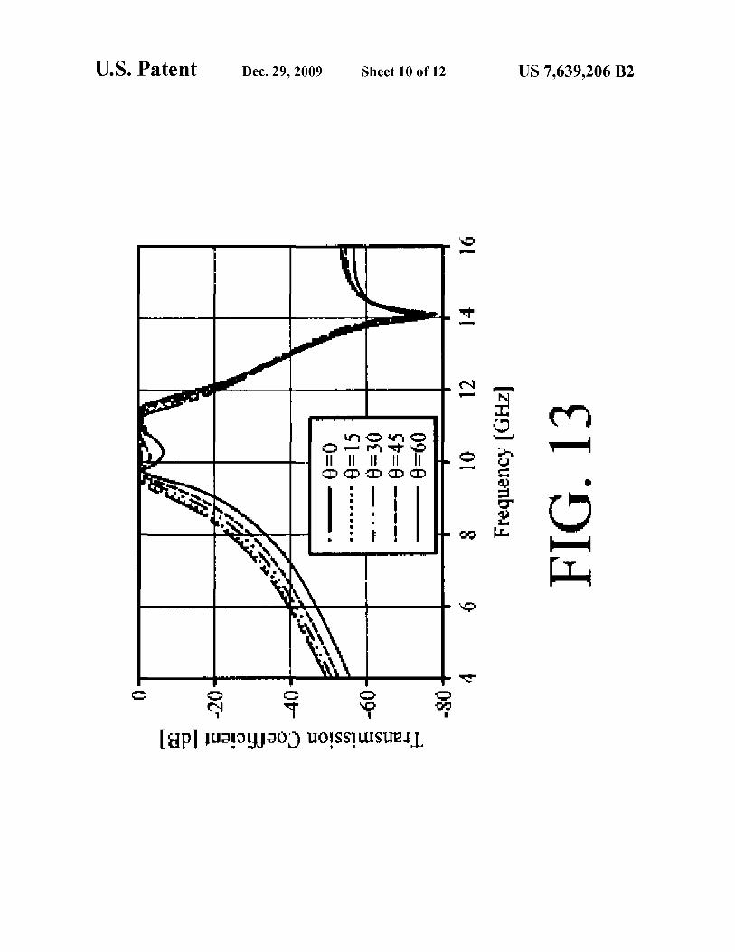
FSS of FIGS. 2-3 disposed thereon.
DETAILED DESCRIPTION
10 disposed between the FSS 202 and high Q FSS 206. The features on FSSs 202, 206 have respective dimensions including physical thicknesses t202 , t206 and spacing's between one another selected in accordance with a particular third-order FSS 200 application (including application frequency). Simi-Embodiments of the invention provide low profile, multi
layer frequency selective surfaces (FSSs) for use in applications including filter applications, reflector applications, and transmission applications. In the filter applications, the low profile, multi-layer FSSs are designed to have higher-order filter responses (e.g., higher order bandpass frequency responses). The phrase "higher-order filter responses", as 20
used herein, refers to an N'h -order filter response, where N has
15 larly, the dielectric layer 208 is disposed between the high Q FSS 206 and FSS 210. The features ofFSS 210 have dimen-
a value equal to or greater than three (e.g., N=3, 4, 5, 6, 7, ... ). The N'h-order multi-layer FSSs have physical thicknesses tN less than the physical thicknesses tc of N'h -order conventional multi-layer FSSs (e.g., tN<a value that corre- 25
sponds to an electrical thickness of O. lA and tc>a value that corresponds to an electrical thickness of 0.5A, where 1 mm corresponds to A/30 for a frequency of 10 GHz). As such, the N'h -order multi-layer FSSs can be used in applications where conformal multi-layer FSSs are required. Such applications 30
include, but are not limited to, aircraft applications, missile applications, ship applications, and other propelled object or vehicle applications. FSSs according to embodiments of the invention have been found to provide low sensitivity's of response to angles of incidence of an incident plane wave. 35
The low-profile, multi-layer FSSs can also be used in antenna applications, radome applications, beam former applications for large antenna arrays, radar cross section reduction applications, spaceborne deployable antenna array applications, electronic counter measure (ECM) applications, and elec- 40
tronic counter measure (ECCM) applications. The invention will now be described more fully hereinafter
with reference to accompanying drawings, in which illustrative embodiments of the invention are shown. This invention, may however, be embodied in many different forms and 45
should not be construed as limited to the embodiments set forth herein.
sions including a physical thickness t210 selected in accordance with a particular third-order FSS 200 application. The dielectric layers 204, 208 can be formed of the same dielectric material or different dielectric materials. The dielectric layers 204, 208 have respective dimensions including physical thicknesses t204, t208 selected in accordance with a particular third-order FSS 200 application. The particular application may also include the selection of the electrically conductive and dielectric materials used to fabricate FSS 200
The high Q FSS has a minimum quality factor Q at its primary resonant frequency. As should be understood, the phrase "quality factor" as used herein refers to a measure for the strength of a damping of a resonator's oscillations and a measure for a relative line-width of a resonator. The loaded quality factor Q can have a minimum value of at least thirty (30) as its primary resonant frequency. As should also be understood, the phrase "loaded quality factor", as used herein, refers to a specific mode of resonance of an FSS when there is external coupling to that mode. The high Q FSS 206 can have a primary resonant frequency that is lower than the primary resonant frequencies of the FSSs 202, 210. Accordingly, the high Q FSS 206 can resonate at a frequency of operation while the FSSs 202 and 210 (above and below FSS 206) can be non-resonant since their operation will be below their primary resonant frequency. The primary resonant fre-quency for FSS 206 can generally be selected to have a value ranging between five hundred megahertz to one hundred gigahertz (500 MHz-100 GHz).
According to an embodiment of the invention, the FSSs 202, 210 each have a resonant frequency of at least thirty percent (30%) higher or 1.3 times the primary resonant frequency of the high Q FSS 206. For example, the FSSs 202, 210 each can have a resonant frequency three (3) times higher
Referring now to FIG. 2, there is provided an enlarged perspective view of a third-order frequency selective surface (FSS) 200 topology according to an embodiment of the invention. A side view of a third-order FSS 200 is provided in FIG. 3. The third-order FSS 200 acts as a spatial band-pass filter with a third-order band-pass response. The phrase "thirdorder band-pass response", as used herein, refers to a filter response characteristic of a third-order system which comprises a sharper out-of-band rejection response as compared to the rejection provided by a second or first-order band-pass filter. Spatial band-pass filters are well known to those having ordinary skill in the art, and therefore will not be described herein. The third-order FSS 200 can be fabricated using any suitable fabrication technique known to those having ordinary skill in the art (e.g., a lithography technique).
50 than the resonant frequency of the high Q FSS 206. The invention is not limited in this regard.
Although the present invention will be described in relation to a third-order FSS 200, the invention is not limited in this regard. The following discussion of the third-order FSS 200 is sufficient for understanding the characteristics and features of other low profile N'h -order FSSs, where N has a value equal to
The third-order FSS 200 has an overall physical thickness t200 . This physical thickness t200 is substantially less than the overall physical thickness of a conventional third-order FSS
55 (such as the FSS shown in FIG. 1). The phrase "substantially less" as used herein means that a physical thickness t of a conventional N'h -order FSS is reduced by a factor larger than or equal to fifty-percent (50%). For example, the overall physical thickness t200 of the third-order FSS 200 generally
60 has a value that corresponds to an electrical thickness falling between one-tenth of a wavelength (A./10) and one-hundredth of a wavelength (A/100). As described above, for a frequency of ten gigahertz (10 GHz), one millimeter (1 mm) corresponds to one-thirtieth of a wavelength (A./30). In contrast, the
65 overall physical thickness t100 of the conventional third-order FSS 100 (shown in FIG. 1) has a value that corresponds to an electrical thickness of one-half of a wavelength (A/2). The

US 7,639,206 B2 5
invention is not limited in this regard. The physical thickness ofan N'h-order FSS according to an embodiment of the invention can have any value equal to the physical thickness of an N'h -order conventional FSS reduced by a factor larger than or equal to fifty (or 2% ).
6 greater than the capacitance of the FSSs 1402, 1418. The FSSs 1406, 1414 can be comprised of the same array of features (or "resonators"). The FSSs 1406, 1414 can have a primary resonant frequency lower than the primary resonant
5 frequencies of the FSSs 1402, 1412, 1418. Accordingly, the FSSs 1406, 1414 can resonate at a frequency of operation having a value between five hundred megahertz to one hundred gigahertz (500 MHz-100 GHz). In contrast, the FSSs 1402, 1412, 1418 may not resonate at the frequency of opera-
This relatively small physical thickness t200 provides a low-profile third-order FSS 200 that overcomes a particular non-conformal drawback of conventional third-order FSSs (such as the third-order FSS 100 shown in FIG. 1). Unlike conventional third-order FSSs (such as the third-order FSS shown in FIG. 1), the low-profile third-order FSS 200 can generally be used on conformal or curved surfaces. The conformal or curved surfaces can include, but are not limited to, the curved surfaces of aircrafts, missiles, ships, and other propelled object or vehicles. A schematic illustration of the 15
low-profile third-order FSS 200 used on a curved surface of the nose of an aircraft is shown in FIG. 16.
10 tion. The invention is not limited in this regard. An enlarged top view of the FSS 202 is provided in FIG. 4.
It should be understood thatthe FSS 210 can bethe same as or substantially similar to the FSS 202. As such, the following discussion of the FSS 202 is generally sufficient for understanding the FSS 210.
Referring now to FIG. 4, the FSS 202 shown is generally a two-dimensional periodic structure with an array 406 of electrically conductive elements 406 1 , ... , 406N The array 406 can include a plurality of periodic electrically conductive structures (e.g., patches) disposed (or printed) on a dielectric layer 204 (described above in relation to FIGS. 2-3) of the
Each FSS 202, 206, 210 of the third-order FSS 200 can generally be a two-dimensional periodic structure with subwavelength unit cell dimensions and/or periodicity. The 20
phrase "unit cell" as used herein refers to a combination of resonant and non-resonant elements. The electrically small period and unit cell dimensions of the third-order FSS 200 allow for localization of band-pass characteristics to within a small area on a surface of the third-order FSS 200. This 25
FSS 200 or embedded in the dielectric layer 204. The periodic metallic structures (e.g., patches) can be disposed on the dielectric layer 204 using any suitable technique known in the art. Such techniques can include, but are not limited to, printing techniques and adhesion techniques. Each of the electri-localization of band-pass characteristics facilitates flexible
spatial filtering for an arbitrary wave phase-front. The small unit cell dimensions and overall physical thickness t200 of the third-order FSS 200 generally results in a reduced sensitivity to an angle of incidence of an electromagnetic (EM) wave as compared to conventional third-order FSSs (such as the thirdorder FSS shown in FIG. 1). The sub-wavelength periodic structure allows for reducing an overall two-dimensional (2D) size of the third-order FSS 200. For example, if the third-order FSS 200 includes a sub-wavelength periodic structure, then the third-order FSS 200 can have an overall two-dimensional (2D) area corresponding to an electrical area of two wavelengths by two wavelengths (21'. by 21'.). The invention is not limited in this regard. The third-order FSS 200 can have an overall two-dimensional (2D) area selected in accordance with a particular third-order FSS 200 application. For example, if a two-dimensional (2D) area of an FSS 200 is defined by the dimensions of fifteen unit cells by fifteen unit cells, then the frequency response of the FSS 200 is a substantially infinite frequency response. Therefore, a desired frequency response can be obtained for a two-dimensional (2D) area defined by the dimensions ofless than fifteen unit cells by fifteen unit cells.
A pair of third-order FSSs 200 can be stacked by sharing a common FSS layer to provide a higher than third-order FSS, such as a fifth-order FSS. The fifth-order FSS can have a low-profile (or physical thickness) corresponding to an electrical thickness on the order of one-fifth of a wavelength (A./5) to a fiftieth ofa wavelength (A/50). This low-profile (or physical thickness) is substantially less than the profile (or physical thickness) of a conventional fifth-order FSS (i.e., a physical thickness of fifth-order FSS is above a wavelength). A schematic illustration of a fifth-order FSS 1400 according to an embodiment of the invention is provided in FIG. 14. As shown in FIG. 14, the first third-order FSS comprises FSSs 1410, 1406, and 1402 while the second third-order FSS comprises FSSs 1418, 1414, and 1410. FSSs 1406 and 1414 are the high Q FSS. Fifth-order FSS 1400 comprises dielectric layers 1404, 1408, 1412, 1416. The dielectric layers 1404, 1408, 1412, 1416 can be formed of the same dielectric material. The FSSs 1402, 1418 can include identical arrays of metallic elements. The FSS 1410 can have a capacitance
cally conductive elements 406 u ... , 406Ncan be formed of an electrically conductive material, such as metal. The array 406 can have a pre-selected length 402 and width 404. Each of the
30 dimensions 402, 404 is selected in accordance with a particular third-order FSS 200 application.
An enlarged top view of electrically conductive elements 406 1 , 4062 , 4063 , 406w 40612, 40621 , 40622, 40623 is provided in FIG. 5. It should be understood that the following
35 discussion is sufficient for understanding the geometries of each electrically conductive element 406 1 , ... , 406N and inter-element spacing of the electrically conductive elements 406 1 , ... , 406N. It should also be understood that the geometries and inter-element spacing contribute to a determination
40 of an overall frequency response of FSS 202 and thus the third-order FSS 200.As such, each of the electrically conductive elements can have an arbitrary geometry selected in accordance with a particular FSS 200 application. Such an arbitrary geometry can include, but is not limited to, a rect-
45 angular geometry (such as the square geometry shown in FIGS. 4-5) and a rectangular geometry with at least one set of digits (not shown).
As shown in FIG. 5, each unit cell 500 has a pre-selected physical length DY and physical width Dx. The physical length
50 DY has a maximum value corresponding to an electrical dimension equal to a period of the third-order FSS 200 in a y direction of a two-dimensional (2D) space. Similarly, the physical width Dx has a maximum value corresponding to an electrical dimension equal to a period of the third-order FSS
55 200 in an x direction of a two-dimensional (2D) space. Each unit cell 500 is comprised of a dielectric portion with a preselective physical width d=s/2, where s is the distance between adjacent electrically conductive elements. Each unit cell 500 is also comprised of a conductive portion defined by
60 an electrically conductive element 406 1 , 4062 , 4063 , 406 11 ,
40612' 40621' 40622' 40623" Each of the electrically conductive elements 406u 4062 ,
4063 , 406w 406w 40621 , 40622 , 40623 is separated from adjacent electrically conductive elements by a pre-selected
65 physical distance d=s. Each of the electrically conductive elements 406u 4062 , 4063 , 406 11 , 406 12, 4062u 40622 , 40623
has a pre-selected length DY-sand width Dx-s. Each of the

US 7,639,206 B2 7
dimensions DY-s, Dx-s is selected in accordance with a particular FSS 200 application. For example, each of the dimensions has DY-s, Dx-s corresponding to an electrical dimension of less than one-wavelength. In effect, the FSS 202 comprising electrically conductive elements 406u 4062 , 5
4063 , 406 1 u 406w 4062 u 40622 , and 40623 is non-resonant at a frequency of operation (e.g., 10 GHz). The periodic arrangement of the electrically conductive elements 4061 ,
4062 , 4063 , 406w 406w 4062 u 40622 , 40623 presents a capacitive impedance in both directions to an incident elec- 10
tromagnetic (EM) wave. Referring now to FIG. 6, there is provided an enlarged top
view of the high Q FSS 206 shown in FIGS. 2-3. The high Q FSS 206 can generally be defined as a two-dimensional periodic structure with an array 606 of dielectric features 15
6061 , ... , 606N. The array 606 of features 6061 , ... , 606Ncan be etched in an electrically conductive layer using any suitable etching technique known in the art. Each of the dielectric features 606 1 , ... , 606Ncan generally comprise a slot resonator. The array 406 of features 606 1 , ... , 606N can have 20
pre-selected dimensions, such as a physical length 602 and a physical width 604. Each of the dimensions 602, 604 is selected in accordance with a particular third-order FSS 200 application.
An enlarged top view of features 606 1 , 6062 , 6063 , 606 11 , 25
60612, 60621 , 60622, 60623 is provided in FIG. 7. It should be understood that the following discussion is sufficient for understanding the geometries of each feature 606 1 , ... , 606N and inter-element spacing of the features 606u ... , 606N. It should also be understood that the geometries and inter-ele- 30
ment spacing contribute to a determination of an overall frequency response of the third-order FSS 200. As such, each of the features 6061 , ... , 606N can have an arbitrary geometry selected in accordance with a particular FSS 200 application. A schematic illustration of a feature 6061 having a first type of 35
geometry according to an embodiment of the invention is provided in FIG. 8. A schematic illustration of a feature having a second type of geometry according to an embodiment of the invention is provided in FIG. 15. It should be noted that the feature shown in FIG. 15 is a dual-polarized 40
crossed slot antenna comprising two straight slots arranged so as to form a cross, wherein each straight slot is connected to two (2) balanced spirals at each of its ends.
Referring now to FIG. 8, the feature 6061 has an exemplary arbitrary geometry defined by electrically conductive por- 45
tions including a straight slot section802 connected to two (2) balanced spirals 804, 806 at each end 808, 810. The straight slot section 802 has a physical width of DK selected in accordance with a particular third-order FSS 200 application. Each spiral of the spirals 804 is separated from an adjacent spiral of 50
the spirals 806 by a certain physical distance DM The physi-cal distance DMis also selected in accordance with a particu-lar third-order FSS 200 application.
8 physical length and physical width having values equal to D ap· In this regard, it should be understood that the overall area of a feature is significantly smaller than a conventional dipole or slot antenna of a first-order FSS (such as that shown in FIG. 1). For example, each features 606u 6062 , 6063 ,
606 1 u 60612, 60621 , 60622 , 60623 has an overall physical area of D apxD ap' where D ap is a fraction of a unit cell size, i.e., Dap<Dx, Dy Each of the features 606 1 , 6062 , 6063 , 606 11 ,
60612, 606w 606w 60623 is a single polarized feature capable of resonating an electric field polarized in a "y" direction of a two-dimensional (2D) space 700. In effect, the frequency response of the third-order FSS 200 becomes polarization sensitive.
Referring now to FIG. 9A, there is provided an equivalent circuit 900 for the third-order FSS 200 (described above in relation to FIGS. 2-7). The equivalent circuit 900 is generally that of a third-order band-pass microwave filter. The operations of a third-order band-pass microwave filter are well known to those having ordinary skill in the art, and therefore will not be described herein. However, a brief discussion of the equivalent circuit 900 is provided to assist a reader in understanding the present invention.
As shown in FIG. 9A, the equivalent circuit 900 is comprised of an input terminal 902, an output terminal 904, capacitors 920, 924, an inductor 926, a feature 950, and short sections of a transmission line (SSTL) 960, 962, 964, 966. The capacitors 920, 924 are connected in parallel between terminals 902, 904 and ground. Each of the capacitors 920, 924 has a capacitance c2.
Thefeature950 is a circuitequivalentofafeature 6061 , ... ,
606N (described above in relation to FIGS. 6-8). As shown in FIG. 9A, the feature 950 is comprised of a capacitor 922 connected in parallel with an inductor 928. The capacitor 922 has a capacitance C1 . The inductor 928 has an inductance L1 .
The feature 950 is connected in series with the inductor 926 having an inductance L2 . The inductor 926 represents a parasitic inductance associated with an electric current flowing in a ground plane of the high Q FSS 206 (described above in relation to FIGS. 6-8), wherein resonant slots are etched in the ground plane. Each of these slots defines a slot antenna. The slot antenna resonates at a frequency determined by the shape of the resonant slots. The inductor 926 is associated with the electric current which has an inductance value inversely proportional to the cross sectional area of the conductor.
The feature 950 is connected in parallel with the capacitors 920, 924. The capacitors 920, 924 represent FSSs 202, 210 (described above in relation to FIGS. 2-3) of the third-order FSS 200 (described above in relation to FIGS. 2-3). The feature 950 is separated from the capacitors 920, 924 with SSTLs 962, 964, respectively. The SSTLs 962, 964 represent the dielectric layer 204, 208 (described above in relation to FIGS. 2-3) of the third-order FSS 200 (described above in relation to FIGS. 2-3). As such, each of the SSTLs 962, 964 has a characteristic impedance Z1 and a length I. The length 1 of each SSTLs 962, 964 has a value equal to the physical thickness t204, t206 of a dielectric layer 204, 208 (described above in relation to FIGS. 2-3). The characteristic impedance Z1 of each SSTLs 962, 964 can be defined by the following mathematical equation (1).
(1)
The effective electrical length E1 of the feature 606 1
extends from a first end of a first balanced spiral 820 to the 55
corresponding end of a second balanced spiral 822. According to an embodiment of the invention, the effective electrical length E1 of the feature 606 1 has a value equal to half of a wavelength (/J2). In such a scenario, the feature 606 1 is a resonant structure acting as a magnetic Herzian dipole. Mag- 60
netic Herzian dipoles are well known to those having ordinary skill in the art, and therefore will not be described herein. The invention is not limited in this regard. The effective electrical length E1 of the feature 606 1 can have any value selected in accordance with a particular third-order FSS application.
where Z0 equals three hundred seventy-seven ohms (the impedance of free space). Er is a dielectric constant of dielec-
65 tric layers 204, 208 (described above in relation to FIGS. 2-3). Referring again to FIG. 7, each of the features 606u 6062 ,
6063 , 606 1 u 60612, 60621 , 60622, 60623 has the same overall The SSTLs 960, 966 represent free space provided on both
sides of the third-order FSS 200 (described above in relation

US 7,639,206 B2 9
to FIGS. 2-3). Each of the SSTLs 960, 966 is a semi-infinite transmission line with a characteristic impedance Z0 .
Although not required to practice the invention, applicant provides the following theoretical background which is help-ful to explain the operations of the multi-layer FSS structure 5
200. Referring now to FIG. 9B, there is provided an expanded equivalent circuit model 990 for the third-order FSS 200 (described above in relation to FIGS. 2-7). As shown in FIG. 9B, the equivalent circuit 990 is comprised of impendence inverters 972, 974, capacitive loaded transmission lines 10
(CLTLs) 970, 976, and a parallel LC resonator 978. Each of the impendence inverters 972, 974 is an inductive network with a transmission line having a "negative" electrical length. The principles and operation ofimpendence inverters are well known to those having ordinary skill in the art, and therefore 15
will not be described herein. Each of the impendence invert-ers 972, 974 is interposed between a respective CLTL 970, 976 and the parallel LC resonator 978. The combination of these circuit components 970, 972, 974, 976, 978 results in a third-order band-pass filter. By comparing the equivalent cir- 20
cuits 900, 990, it is observed that the "negative" electrical length of each transmission line used in the impendence inverters 972, 974 is absorbed in a "positive" electrical length of a respective CLTL 970, 976. The inductors L, of the impendence inverters 972, 974 are absorbed in the parallel LC 25
resonator 978. The following FIG. 10 and accompanying text illustrate a
design process 1000 for designing an N'h-order FSS according to an embodiment of the invention (such as the third-order FSS 200 ofFIGS. 2-8). It should be appreciated, however, that 30
the design process disclosed herein is provided for purposes ofillustration only and that the present invention is not limited solely to the design process shown.
Referring now to FIG. 10, the design process 1000 begins at step 1002 and continues with step 1004. In step 1004, 35
element values Cu C2 , L1 , L2 , Z0 , Z1 , 1, Er are obtained for an equivalent circuit 900. These element values can be obtained using any suitable circuit simulation software known to those having ordinary skill in the art. Such circuit simulation software includes, but is not limited to, Advanced Design Sys- 40
terns available from Agilent Technologies of Santa Clara, Calif.
10 spirals 804, 806 at each end 808, 810. The effective electrical length E1 of the feature 606 1 has a value approximately equal to half of a wavelength (A./2). As such, the feature 606 1 is a resonant structure acting as a magnetic Herzian dipole. The quality factor Q of the feature 606u ... 606N is inversely proportional to the area (DapDap) occupied by the features 606 1 , ... , 606N. The quality factorQ of the features 6061 , ... ,
606N can be increased by reducing the area (Dap·Dap) occupied by the features 606u ... , 606N while maintaining the resonant frequency of the features 6061 , ... 606Nin effect, the desired element values Lu C1 can be obtained by selecting aperture dimensions of the features 606u ... , 606N for a constant resonant frequency. The invention is not limited in this regard.
According to an embodiment of the invention, step 1006 involves designing a feature 606u ... , 606N using full-wave electromagnetic (FWEM) simulations in conjunction with circuit based simulation. In such a scenario, a portion of a unit cell (PUC) of a proposed third-order FSS is simulated by performing full-wave electromagnetic (EM) simulations using HFSS® simulation software available from Ansoft Corporation of Pittsburg, Pa. A schematic illustration of a simulation model 1100 including a topology for the PUC is provided in FIG. llA. As shown in FIG. llA, the PUC 1102 can comprise a feature 1122 sandwiched between two dielectric substrates 1120, 1124. The PUC 1102 is placed in a waveguide 1130. The waveguide 1130 has periodic boundary conditions for emulating an infinite structure. Step 1006 also involves performing Finite Element Method (FEM) simulations to calculate transmission and reflection coefficient of a vertically polarized transverse electromagnetic (TEM) wave. Step 1006 further involves performing a circuit based (CB) simulation of a relevant portion 910 of an equivalent circuit 900 (described above in relation to FIG. 9A). After performing the FWEM, FEM, and CB simulations, a matching process is performed. This matching process can generally involve matching the results of the FWEM simulations to results obtained from the CB simulation. The matching process can also involve modifying the dimensions of a feature 1122 in accordance with the outcome of matching the FWEM and CB simulation results. This matching process can be iteratively performed until a frequency response obtained through the FWEM simulations are matched to the frequency response of the relevant portion 910 of an equivalent circuit
According to an embodiment of the invention, each of the dielectric layers 204, 208 of a third-order FSS 200 is formed of a dielectric substrate having a physical thickness of half a millimeter (t204=0.5 mm, t206=0.5 mm). The equivalent circuit 900 has a band-pass frequency response with a center frequency of operation often gigahertz (10 GHz) and a fractional bandwidth of twenty percent (20% ). In such a scenario, the equivalent circuit 900 element values obtained in step 1004 of design process 1000 can be defined as: C1=22.2 pF; C2 0.38 pF; L1=108 pH; L2 =147 pH; Z0=377Q; Z1=254Q; 1=0.5 mm; and Er=2.2. The invention is not limited in this regard.
45 900 (described above in relation to FIG. 9A). The invention is not limited in this regard.
Referring again to FIG. 10, the design process 1000 continues with step 1006. In step 1006, a feature 606u ... , 606N is designed for a high Q FSS 206 (described above in relation to FIGS. 2-3) of a third-order FSS 200 (described above in relation to FIGS. 2-3). The feature 606u ... , 606N can be designed by performing full-wave electromagnetic (EM) simulations in conjunction with a circuit based simulation. The feature 606u ... , 606N can be designed so that it has element values C606, L606 matching the element values Cu L1
obtained in the previous step 1004. According to an embodiment of the invention, the feature
6061 , ... , 606Ncan generally be a slot antenna composed of a straight slot section 802 connected to two (2) balanced
Referring again to FIG. 10, the design process 1000 continues with step 1008. In step 1008, the electrically conductive elements 406 1 , ... , 406N are designed for an FSS 202,
50 210 (described above in relation to FIGS. 2-3) ofa third-order FSS 200 (described above in relation to FIGS. 2-3). The electrically conductive elements 406u ... , 406N can be designed by performing full-wave simulations of a unit cell for a proposed FSS. The electrically conductive elements
55 406 1 , ... , 406N can be designed so that they have element values c406 matching the element values c2 obtained in the previous step 1004.
According to an embodiment of the invention, the electrically conductive elements 4061 , ... , 406N are designed by
60 adding two (2) electrically conductive elements 1150, 1152 to the full-wave simulation model 1100 (as showninFIG. llB). The two (2) electrically conductive elements 1150, 1152 correspond to a capacitor 920, 924 (described above in relation to FIG. 9A) of the equivalent circuit 900 (described above in
65 relation to FIG. 9A). The electrically conductive elements 1150, 1152 are sub-wavelength, non-resonant patches with physical lengths 1 =D-s and physical widths w= 1 =D-s,

US 7,639,206 B2 11
where D has a value corresponding to the period of the fullwave simulation model 1100 and s is the distance between adjacent electrically conductive elements of a proposed FSS. D can have a value equal to the physical length DY and physical width Dx of a unit cell. The initial dimension 1 of the 5
electrically conductive elements 1150, 1152 is approximated using the following mathematical equation (2).
C~E0Eeffi(2(D-s))ht] log [1/(sin(ns/(2(D-s))))] (2)
12 a rather stable frequency response as a function of angle of incidence without the aid of any dielectric superstrates that are commonly used to stabilize the frequency response of FSSs for oblique angles of incidence.
All of the apparatus, methods and algorithms disclosed and claimed herein can be made and executed without undue experimentation in light of the present disclosure. While the invention has been described in terms of preferred embodiments, it will be apparent to those of skill in the art that
where C is a capacitance of a electrically conductive element of an FSS measured in Farads. E 0 is the permittivity of free space and has value of 8.85·10-12 F/m. Eeffis the effective dielectric constant of the dielectric layers 204, 208 (described above in relation to FIGS. 2-3). D is a unit cell dimension corresponding to the periodicity of an FSS, where Dx =DY =Ds is a physical distance between two adjacent electrically conductive elements of the FSS. it has a value equal to 3.1415.
10 variations may be applied to the apparatus, methods and sequence of steps of the method without departing from the concept, spirit and scope of the invention. More specifically, it will be apparent that certain components may be added to, combined with, or substituted for the components described
15 herein while the same or similar results would be achieved.
After adding the electrically conductive elements 1150, 1152 to the full-wave simulation model 1100, full-wave
20 simulations are performed using the modified full-wave simulation model 1100 (as shown in FIG. llB). It should be noted that the modified full-wave simulation model 1100 shown in FIG. llB represents a unit cell of a proposed FSS. Upon completing the full-wave simulations, the physical
25 dimensions 1, w of the electrically conductive elements 1150, 1152 are adjusted based on the results of the full-wave simulations. This full-wave simulation and dimension adjustment process is repeated until the frequency response of the modified full-wave simulation model 1100 matches a desirable
30 frequency response of a proposed multi-layer FSS. The invention is not limited in this regard.
The following Example is provided in order to further illustrate the design process 1000. The scope of the invention, however, is not to be considered limited in any way thereby. 35
EXAMPLE
A third-order FSS 200 having an equivalent circuit 900 was designed using design process 1000. The circuit elements of 40
the equivalent circuit 900 used in the design process 1000 were defined as: C1=22.2 pF; C2=0.38 pF; L1=108 pH; L2 =147 pH; Z0 =377Q; Z1=254Q; 1=0.5 mm; and Er=2.2. The physical and geometrical parameters for the third-order FSS 900 obtained during the design process 1000 were 45
defined as: Dx=5.5 mm; DY =5.5 mm; t200=0.5 mm; Er=2.2; s=60 µm; and D ap = 1.46 mm.
The frequency response between four and sixteen gigahertz ( 4 GHz-16 GHz) of the third-order FSS 200 obtained from FWEM simulations is shown graphically in FIG. 12. 50
The frequency response of the equivalent circuit 900 obtained from CB simulations is also shown graphically in FIG. 12. As shown in FIG. 12, the equivalent circuit 900 accurately predicted the frequency response of the third-order FSS 200. A calculated frequency response of the third-order FSS 200 for 55
non-normal angles of incidence (8=15°, 30°, 45°, and 60°) is shown graphically in FIG. 13. As shown in FIG. 13, the transmission coefficient of the third-order FSS 200 is provided for an obliquely incident plane wave for various angles of incident ranges from zero degrees to sixty degrees (0° to 60
60°). The frequency response of the third-order FSS 200 was not considerably affected as the angle of incidence increases from zero degrees to forty-five degrees (0° to 45°). However, the frequency response of the third-order FSS 200 was affected as the angle of incidence increases from forty-five 65
degrees to N degrees ( 45° to N°), whereN is anintegergreater than forty-five ( 45). Nevertheless, the structure demonstrated
All such similar substitutes and modifications apparent to those skilled in the art are deemed to be within the spirit, scope and concept of the invention as defined.
The Abstract of the Disclosure is provided to comply with 37 C.F.R. § 1.72(b), requiring an abstract that will allow the reader to quickly ascertain the nature of the technical disclosure. It is submitted with the understanding that it will not be used to interpret or limit the scope or meaning of the following claims.
I claim: 1. A frequency selective surface-based (PSS-based) device
for processing electromagnetic waves, comprising: a first and second frequency selective surface (FSS) having
first and second primary resonant frequencies, respectively;
a high quality factor (Q) FSS having a lower primary resonant frequency relative to said first and second primary resonant frequencies, said high Q FSS interposed between said first and second FSS and having a loaded Q of at least thirty at said lower primary resonant frequency;
a first dielectric layer interposed between said first FSS and said high Q FSS; and
a second dielectric layer interposed between said second FSS and said high Q FSS.
2. The PSS-based device according to claim 1, wherein said high Q FSS comprises a plurality of dielectric comprising features formed in an electrically conductive layer.
3. The PSS-based device according to claim 2, wherein said high Q FSS comprises a plurality of slot antennas.
4. The PSS-based device according to claim 3, wherein said slot antennas comprise a straight slot having a set of balanced spirals disposed at each end of said straight slot.
5. The PSS-based device according to claim 3, wherein said slot antenna comprises a dual-polarized crossed slot antenna.
6. The PSS-based device according to claim 1, wherein a thickness of said PSS-based device is <A/10, where A is a wavelength of operation of said PSS-based device.
7. The PSS-based device according to claim 1, further comprising a plurality of PSS-based devices stacked together by sharing at least one common layer selected from said first and second FSS.
8. The PSS-based device according to claim 1, wherein said first and second primary resonant frequencies are each at least 1.3 times larger than said lower primary resonant frequency.
9. The PSS-based device according to claim 1, wherein said first and second primary resonant frequencies are each at least three times larger than said lower primary resonant frequency.

US 7,639,206 B2 13
10. A system, comprising: a propelled object or vehicle; and
14 12. The system according to claim 11, wherein said high Q
PSS comprises a plurality of slot antennas. 13. The system according to claim 12, wherein said slot
antennas comprise a straight slot having a set of balanced spirals disposed at each end of said straight slot.
a frequency selective surface based (PSS-based) device coupled to said propelled object or vehicle, said PSSbased device configured for processing electromagnetic waves and comprising a substrate having a surface layer; and
14. The system according to claim 12, wherein said slot antenna comprises a dual-polarized crossed slot antenna.
15. The system according to claim 10, wherein a thickness of said multi-layer PSS structure is <A.110, where A is a wave-
10 length of operation of said PSS-based device.
a multi-layer frequency selective surface (PSS) structure disposed on said surface layer, said multi-layer PSS structure comprising a first PSS having a first primary resonant frequency, a second PSS having a second primary resonant frequency, a high quality factor (Q) PSS interposed between said first PSS and said second PSS, a first dielectric layer interposed between said first PSS and said high Q PSS, and a second 15
dielectric layer interposed between said second PSS and said high Q PSS;
wherein said high Q PSS has a lower primary resonant frequency relative to said first and second primary resonant frequencies and a loaded Q of at least thirty at said lower primary resonant frequency.
11. The system according to claim 10, wherein said high Q PSS comprises a plurality of dialectic comprising features formed in an electrically conductive layer.
16. The system according to claim 10, wherein said multilayer PSS structure comprises a plurality of PSS-based devices stacked together by sharing at least one common layer selected from said first and second PSSs.
17. The system according to claim 10, wherein said first and second primary resonant frequencies are each at least 1.3 times larger than said lower primary resonant frequency.
18. The system according to claim 10, wherein each of said first and second primary resonant frequencies are each at least
20 three times larger than said lower primary resonant frequency. 19. The system according to claim 10, wherein said pro
pelled object or vehicle is an aircraft, a missile, or a ship.
* * * * *