Embed Size (px)
Citation preview

LT1469
11469fb
TYPICAL APPLICATION
FEATURES
APPLICATIONS
DESCRIPTION
Dual 90MHz, 22V/µs 16-Bit Accurate Operational Amplifier
The LT®1469 is a dual, precision high speed operational amplifier with 16-bit accuracy and 900ns settling to 150µV for 10V steps. This unique blend of precision and AC performance makes the LT1469 the optimum choice for high accuracy applications such as DAC current-to-voltage conversion and ADC buffers. The initial accuracy and drift characteristics of the input offset voltage and inverting input bias current are tailored for inverting applications.
The 90MHz gain bandwidth ensures high open-loop gain at frequency for reducing distortion. In noninverting ap-plications such as an ADC buffer, the low distortion and DC accuracy allow full 16-bit AC and DC performance.
The 22V/µs slew rate of the LT1469 improves large signal performance compared to other precision op amps in applications such as active filters and instrumentation amplifiers.
The LT1469 is available in a space saving 4mm × 4mm leadless package, as well as in small outline and DIP pack-ages. A single version, the LT1468, is also available.
16-Bit DAC I-to-V Converter and Reference Inverter for Bipolar Output Swing (VOUT = –10V to 10V)
n 90MHz Gain Bandwidth, f = 100kHzn Maximum Input Offset Voltage: 125µVn Settling Time: 900ns (AV = –1, 150µV, 10V Step)n 22V/µs Slew Raten Low Distortion: –96.5dB for 100kHz, 10VP-Pn Maximum Input Offset Voltage Drift: 3µV/°Cn Maximum Inverting Input Bias Current: 10nAn Minimum DC Gain: 300V/mVn Minimum Output Swing into 2k: ±12.8Vn Unity-Gain Stablen Input Noise Voltage: 5nV/√Hzn Input Noise Current: 0.6pA/√Hzn Total Input Noise Optimized for 1kΩ < RS < 20kΩn Specified at ±5V and ±15V Supplies
n Precision Instrumentationn High Accuracy Data Acquisition Systemsn 16-Bit DAC Current-to-Voltage Convertern ADC Buffern Low Distortion Active Filtersn Photodiode Amplifiers
Bipolar Multiplying Mode (LTC1597) Signal-to-(Noise + Distortion)
15pF
2.4µs SETTLING TIMETO 1LSB ON 20V STEP
RLPFLTC159716 BITS
DAC INPUTS
VREF
1469 TA01
15pF
CLPF
VOUT
–
+
–
+
1/2 LT1469
1/2 LT1469
12k12k12k12k
–15V
15V
FREQUENCY (Hz)
90
SIGN
AL/(N
OISE
+ D
ISTO
RTIO
N) (d
B)
70
50
40
10 1k 10k 100k
1469 TA01a
110100
60
80
100
DAC INPUT CODE = ALL ZEROSVREF = 20VP-P
500kHz FILTER
80kHz FILTER30kHz FILTER
L, LT, LTC, LTM, Linear Technology and the Linear logo are registered trademarks of Linear Technology Corporation. All other trademarks are the property of their respective owners.
LT1469
21469fb
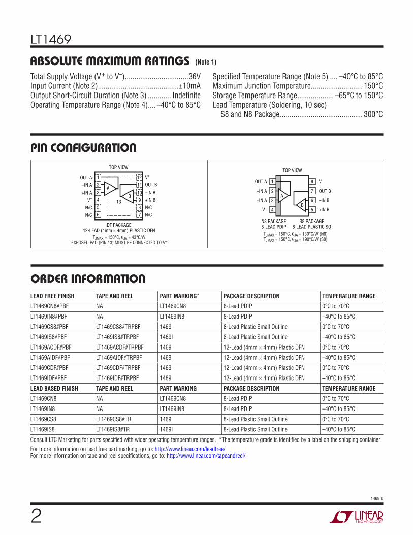
ABSOLUTE MAXIMUM RATINGSTotal Supply Voltage (V + to V–) .................................36VInput Current (Note 2) ..........................................±10mAOutput Short-Circuit Duration (Note 3) ............ IndefiniteOperating Temperature Range (Note 4).... –40°C to 85°C
(Note 1)
TOP VIEW
DF PACKAGE12-LEAD (4mm × 4mm) PLASTIC DFN
12
11
8
9
104
5
3
2
1 V+
OUT B
–IN B
+IN B
N/C
N/C
OUT A
–IN A
+IN A
V–
N/C
N/C 6 7
A
B13
TJMAX = 150°C, θJA = 43°C/W
EXPOSED PAD (PIN 13) MUST BE CONNECTED TO V–
1
2
3
4
8
7
6
5
TOP VIEW
V+
OUT B
–IN B
+IN B
OUT A
–IN A
+IN A
V–
S8 PACKAGE8-LEAD PLASTIC SO
N8 PACKAGE8-LEAD PDIP
A
B
TJMAX = 150°C, θJA = 130°C/W (N8) TJMAX = 150°C, θJA = 190°C/W (S8)
PIN CONFIGURATION
ORDER INFORMATIONLEAD FREE FINISH TAPE AND REEL PART MARKING* PACKAGE DESCRIPTION TEMPERATURE RANGE
LT1469CN8#PBF NA LT1469CN8 8-Lead PDIP 0°C to 70°C
LT1469IN8#PBF NA LT1469IN8 8-Lead PDIP –40°C to 85°C
LT1469CS8#PBF LT1469CS8#TRPBF 1469 8-Lead Plastic Small Outline 0°C to 70°C
LT1469IS8#PBF LT1469IS8#TRPBF 1469I 8-Lead Plastic Small Outline –40°C to 85°C
LT1469ACDF#PBF LT1469ACDF#TRPBF 1469 12-Lead (4mm × 4mm) Plastic DFN 0°C to 70°C
LT1469AIDF#PBF LT1469AIDF#TRPBF 1469 12-Lead (4mm × 4mm) Plastic DFN –40°C to 85°C
LT1469CDF#PBF LT1469CDF#TRPBF 1469 12-Lead (4mm × 4mm) Plastic DFN 0°C to 70°C
LT1469IDF#PBF LT1469IDF#TRPBF 1469 12-Lead (4mm × 4mm) Plastic DFN –40°C to 85°C
LEAD BASED FINISH TAPE AND REEL PART MARKING PACKAGE DESCRIPTION TEMPERATURE RANGE
LT1469CN8 NA LT1469CN8 8-Lead PDIP 0°C to 70°C
LT1469IN8 NA LT1469IN8 8-Lead PDIP –40°C to 85°C
LT1469CS8 LT1469CS8#TR 1469 8-Lead Plastic Small Outline 0°C to 70°C
LT1469IS8 LT1469IS8#TR 1469I 8-Lead Plastic Small Outline –40°C to 85°C
Consult LTC Marketing for parts specified with wider operating temperature ranges. *The temperature grade is identified by a label on the shipping container.For more information on lead free part marking, go to: http://www.linear.com/leadfree/ For more information on tape and reel specifications, go to: http://www.linear.com/tapeandreel/
Specified Temperature Range (Note 5) .... –40°C to 85°CMaximum Junction Temperature........................... 150°CStorage Temperature Range ................... –65°C to 150°CLead Temperature (Soldering, 10 sec)
S8 and N8 Package ........................................... 300°C

LT1469
31469fb
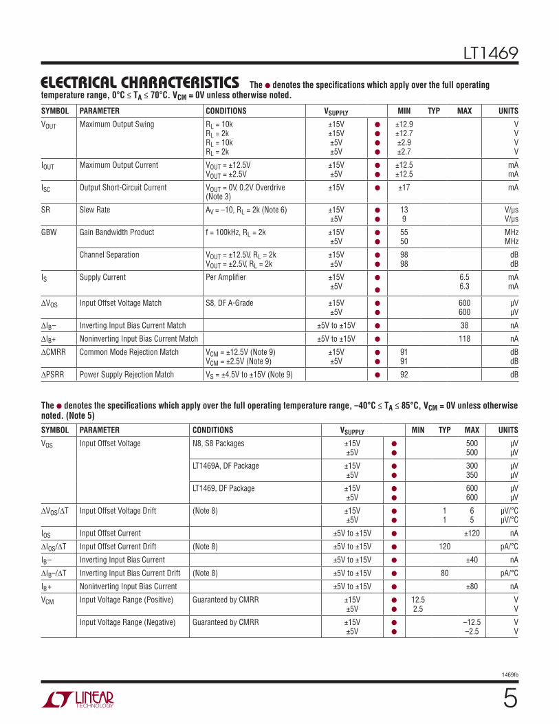
ELECTRICAL CHARACTERISTICS TA = 25°C, VCM = 0V unless otherwise noted.
SYMBOL PARAMETER CONDITIONS VSUPPLY MIN TYP MAX UNITS
VOS Input Offset Voltage N8, S8 Packages ±15V ±5V
50 50
125 200
µV µV
LT1469A, DF Package ±15V ±5V
50 50
125 200
µV µV
LT1469, DF Package ±15V ±5V
100 150
225 300
µV µV
IOS Input Offset Current ±5V to ±15V 13 ±50 nA
IB– Inverting Input Bias Current ±5V to ±15V 3 ±10 nA
IB+ Noninverting Input Bias Current ±5V to ±15V –10 ±40 nA
Input Noise Voltage 0.1Hz to 10Hz ±5V to ±15V 0.3 µVP-P
en Input Noise Voltage Density f = 10kHz ±5V to ±15V 5 nV/√Hz
in Input Noise Current Density f = 10kHz ±5V to ±15V 0.6 pA/√Hz
RIN Input Resistance Common Mode, VCM = ±12.5V Differential
±15V ±15V
100 50
240 150
MΩ kΩ
CIN Input Capacitance ±15V 4 pF
VCM Input Voltage Range (Positive) Guaranteed by CMRR ±15V ±5V
12.5 2.5
13.5 3.6
V V
Input Voltage Range (Negative) Guaranteed by CMRR ±15V ±5V
–14.3 –4.4
–12.5 –2.5
V V
CMRR Common Mode Rejection Ratio VCM = ±12.5V VCM = ±2.5V
±15V ±5V
96 96
110 112
dB dB
Minimum Supply Voltage Guaranteed by PSRR ±2.5 ±4.5 V
PSRR Power Supply Rejection Ratio VS = ±4.5V to ±15V 100 112 dB
AVOL Large-Signal Voltage Gain VOUT = ±12.5V, RL = 10k VOUT = ±12.5V, RL = 2k VOUT = ±2.5V, RL = 10k VOUT = ±2.5V, RL = 2k
±15V ±15V ±5V ±5V
300 300 200 200
2000 2000 8000 8000
V/mV V/mV V/mV V/mV
VOUT Maximum Output Swing RL = 10k RL = 2k RL = 10k RL = 2k
±15V ±15V ±5V ±5V
±13.0 ±12.8 ±3.0 ±2.8
±13.6 ±13.5 ±3.7 ±3.6
V V V V
IOUT Maximum Output Current VOUT = ±12.5V VOUT = ±2.5V
±15V ±5V
±15 ±15
±22 ±22
mA mA
ISC Output Short-Circuit Current VOUT = 0V, 0.2V Overdrive (Note 3) ±15V ±25 ±40 mA
SR Slew Rate AV = –10, RL = 2k (Note 6) ±15V ±5V
15 11
22 17
V/µs V/µs
FPBW Full-Power Bandwidth 10V Peak, (Note 7) 3V Peak, (Note 7)
±15V ±5V
350 900
kHz kHz
GBW Gain Bandwidth Product f = 100kHz, RL = 2k ±15V ±5V
60 55
90 88
MHz MHz
tr, tf Rise Time, Fall Time AV = 1, 10% to 90%, 0.1V Step ±15V ±5V
11 12
ns ns
OS Overshoot AV = 1, 0.1V Step ±15V ±5V
30 35
% %
tPD Propagation Delay AV = 1, 50% VIN to 50% VOUT, 0.1V Step ±15V ±5V
9 10
ns ns

LT1469
41469fb
ELECTRICAL CHARACTERISTICS TA = 25°C. VCM = 0V unless otherwise noted.
SYMBOL PARAMETER CONDITIONS VSUPPLY MIN TYP MAX UNITS
tS Settling Time 10V Step, 0.01%, AV = –1 10V Step, 150µV, AV = –1 5V Step, 0.01%, AV = –1
±15V ±15V ±5V
760 900 770
ns ns ns
THD Total Harmonic Distortion AV = –1, VOUT = 10VP-P, f = 100kHz AV = 1, VOUT = 20VP-P, f = 1kHz
±15V ±15V
–96.5 –125
dB dB
ROUT Output Resistance AV = 1, f = 100kHz ±15V 0.02 Ω
Channel Separation VOUT = ±12.5V, RL = 2k VOUT = ±2.5V, RL = 2k
±15V ±5V
100 100
130 130
dB dB
IS Supply Current Per Amplifier ±15V ±5V
4.1 3.8
5.2 5
mA mA
∆VOS Input Offset Voltage Match S8, DF A-Grade ±15V ±5V
30 50
225 350
µV µV
∆IB– Inverting Input Bias Current Match ±5V to ±15V 2 18 nA
∆IB+ Noninverting Input Bias Current Match ±5V to ±15V 5 78 nA
∆CMRR Common Mode Rejection Match VCM = ±12.5V (Note 9) VCM = ±2.5V (Note 9)
±15V ±5V
93 93
113 115
dB dB
∆PSRR Power Supply Rejection Match VS = ±4.5V to ±15V (Note 9) 97 115 dB
The l denotes the specifications which apply over the full operating temperature range, 0°C ≤ TA ≤ 70°C. VCM = 0V unless otherwise noted.
SYMBOL PARAMETER CONDITIONS VSUPPLY MIN TYP MAX UNITS
VOS Input Offset Voltage N8, S8 Packages ±15V ±5V
350 350
µV µV
LT1469A, DF Package ±15V ±5V
225 275
µV µV
LT1469, DF Package ±15V ±5V
450 450
µV µV
∆VOS/∆T Input Offset Voltage Drift (Note 8) ±15V ±5V
1 1
5 3
µV/°C µV/°C
IOS Input Offset Current ±5V to ±15V ±80 nA
∆IOS/∆T Input Offset Current Drift (Note 8) ±5V to ±15V 60 pA/°C
IB– Inverting Input Bias Current ±5V to ±15V ±20 nA
∆IB–/∆T Inverting Input Bias Current Drift (Note 8) ±5V to ±15V 40 pA/°C
IB+ Noninverting Input Bias Current ±5V to ±15V ±60 nA
VCM Input Voltage Range (Positive) Guaranteed by CMRR ±15V ±5V
12.5 2.5
V V
Input Voltage Range (Negative) Guaranteed by CMRR ±15V ±5V
–12.5 –2.5
V V
CMRR Common Mode Rejection Ratio VCM = ±12.5V ±15V 94 dB
VCM = ±2.5V ±5V 94 dB
Minimum Supply Voltage Guaranteed by PSRR ±4.5 V
PSRR Power Supply Rejection Ratio VS = ±4.5V to ±15V 95 dB
AVOL Large-Signal Voltage Gain VOUT = ±12.5V, RL = 10k VOUT = ±12.5V, RL = 2k VOUT = ±2.5V, RL = 10k VOUT = ±2.5V, RL = 2k
±15V ±15V ±5V ±5V
100 100 100 100
V/mV V/mV V/mV V/mV
LT1469
51469fb
ELECTRICAL CHARACTERISTICS The l denotes the specifications which apply over the full operating temperature range, 0°C ≤ TA ≤ 70°C. VCM = 0V unless otherwise noted.
SYMBOL PARAMETER CONDITIONS VSUPPLY MIN TYP MAX UNITS
VOUT Maximum Output Swing RL = 10k RL = 2k RL = 10k RL = 2k
±15V ±15V ±5V ±5V
±12.9 ±12.7 ±2.9 ±2.7
V V V V
IOUT Maximum Output Current VOUT = ±12.5V VOUT = ±2.5V
±15V ±5V
±12.5 ±12.5
mA mA
ISC Output Short-Circuit Current VOUT = 0V, 0.2V Overdrive (Note 3)
±15V ±17 mA
SR Slew Rate AV = –10, RL = 2k (Note 6) ±15V ±5V
13 9
V/µs V/µs
GBW Gain Bandwidth Product f = 100kHz, RL = 2k ±15V ±5V
55 50
MHz MHz
Channel Separation VOUT = ±12.5V, RL = 2k VOUT = ±2.5V, RL = 2k
±15V ±5V
98 98
dB dB
IS Supply Current Per Amplifier ±15V ±5V
6.5 6.3
mA mA
∆VOS Input Offset Voltage Match S8, DF A-Grade ±15V ±5V
600 600
µV µV
∆IB– Inverting Input Bias Current Match ±5V to ±15V 38 nA
∆IB+ Noninverting Input Bias Current Match ±5V to ±15V 118 nA
∆CMRR Common Mode Rejection Match VCM = ±12.5V (Note 9) VCM = ±2.5V (Note 9)
±15V ±5V
91 91
dB dB
∆PSRR Power Supply Rejection Match VS = ±4.5V to ±15V (Note 9) 92 dB
The l denotes the specifications which apply over the full operating temperature range, –40°C ≤ TA ≤ 85°C, VCM = 0V unless otherwise noted. (Note 5)
SYMBOL PARAMETER CONDITIONS VSUPPLY MIN TYP MAX UNITS
VOS Input Offset Voltage N8, S8 Packages ±15V ±5V
500 500
µV µV
LT1469A, DF Package ±15V ±5V
300 350
µV µV
LT1469, DF Package ±15V ±5V
600 600
µV µV
∆VOS/∆T Input Offset Voltage Drift (Note 8) ±15V ±5V
1 1
6 5
µV/°C µV/°C
IOS Input Offset Current ±5V to ±15V ±120 nA
∆IOS/∆T Input Offset Current Drift (Note 8) ±5V to ±15V 120 pA/°C
IB– Inverting Input Bias Current ±5V to ±15V ±40 nA
∆IB–/∆T Inverting Input Bias Current Drift (Note 8) ±5V to ±15V 80 pA/°C
IB+ Noninverting Input Bias Current ±5V to ±15V ±80 nA
VCM Input Voltage Range (Positive) Guaranteed by CMRR ±15V ±5V
12.5 2.5
V V
Input Voltage Range (Negative) Guaranteed by CMRR ±15V ±5V
–12.5 –2.5
V V

LT1469
61469fb
ELECTRICAL CHARACTERISTICS The l denotes the specifications which apply over the full operating temperature range, –40°C ≤ TA ≤ 85°C, VCM = 0V unless otherwise noted. (Note 5)
SYMBOL PARAMETER CONDITIONS VSUPPLY MIN TYP MAX UNITS
CMRR Common Mode Rejection Ratio VCM = ±12.5V VCM = ±2.5V
±15V ±5V
92 92
dB dB
Minimum Supply Voltage Guaranteed by PSRR ±4.5 V
PSRR Power Supply Rejection Ratio VS = ±4.5V to ±15V 93 dB
AVOL Large-Signal Voltage Gain VOUT = ±12,5V, RL = 10k VOUT = ±12.5V, RL = 2k VOUT = ±2.5V, RL = 10k VOUT = ±2.5V, RL = 2k
±15V ±15V ±5V ±5V
75 75 75 75
V/mV V/mV V/mV V/mV
VOUT Maximum Output Swing RL = 10k RL = 2k RL = 10k RL = 2k
±15V ±15V ±5V ±5V
±12.8 ±12.6 ±2.8 ±2.6
V V V V
IOUT Maximum Output Current VOUT = ±12.5V VOUT = ±2.5V
±15V ±5V
±7 ±7
mA mA
ISC Output Short-Circuit Current VOUT = 0V, 0.2V Overdrive (Note 3) ±15V ±12 mA
SR Slew Rate AV = –10, RL = 2k (Note 6) ±15V ±5V
9 6
V/µs V/µs
GBW Gain Bandwidth Product f = 100kHz, RL = 2k ±15V ±5V
45 40
MHz MHz
Channel Separation VOUT = ±12.5V, RL = 2k VOUT = ±2.5V, RL = 2k
±15V ±5V
96 96
dB dB
IS Supply Current Per Amplifier ±15V ±5V
7 6.8
mA mA
∆VOS Input Offset Voltage Match S8, DF A-Grade ±15V ±5V
800 800
µV µV
∆IB– Inverting Input Bias Current Match ±5V to ±15V 78 nA
∆IB+ Noninverting Input Bias Current Match
±5V to ±15V 158 nA
∆CMRR Common Mode Rejection Match VCM = ±12.5V (Note 9) VCM = ±2.5V (Note 9)
±15V ±5V
89 89
dB dB
∆PSRR Power Supply Rejection Match VS = ±4.5V to ±15V (Note 9) 90 dB
Note 1: Stresses beyond those listed under Absolute Maximum Ratings may cause permanent damage to the device. Exposure to any Absolute Maximum Rating condition for extended periods may affect device reliability and lifetime.Note 2: The inputs are protected by back-to-back diodes and two 100Ω series resistors. If the differential input voltage exceeds 0.7V, the input current should be limited to less than 10mA. Input voltages outside the supplies will be clamped by ESD protection devices and input currents should also be limited to less than 10mA.Note 3: A heat sink may be required to keep the junction temperature below absolute maximum when the output is shorted indefinitely.Note 4: The LT1469C and LT1469I are guaranteed functional over the operating temperature range of –40°C to 85°C.
Note 5: The LT1469C is guaranteed to meet specified performance from 0°C to 70°C and is designed, characterized and expected to meet specified performance from –40°C to 85°C but is not tested or QA sampled at these temperatures. The LT1469I is guaranteed to meet specified performance from –40°C to 85°C.Note 6: Slew rate is measured between ±8V on the output with ±12V swing for ±15V supplies and ±2V on the output with ±3V swing for ±5V supplies.Note 7: Full-power bandwidth is calculated from the slew rate. FPBW = SR/2πVP.Note 8: This parameter is not 100% tested.Note 9: ∆CMRR and ∆PSRR are defined as follows: 1) CMRR and PSRR are measured in µV/V on each amplifier; 2) the difference between the two sides is calculated in µV/V; 3) the result is converted to dB.

LT1469
71469fb
TYPICAL PERFORMANCE CHARACTERISTICS
Distribution of Input Offset Voltage
Distribution of Inverting Input Bias Current
Supply Current vs Supply Voltage and Temperature
Input Noise Spectral Density
0.1Hz to 10Hz Voltage Noise
Total Noise vs UnmatchedSource Resistance
Input Bias Current vs Temperature
Input Bias Current vs Input Common Mode Voltage
Input Common Mode Rangevs Supply Voltage
INPUT OFFSET VOLTAGE (µV)–175
PERC
ENTA
GE O
F UN
ITS
(%)
–125 –75 –25 25 75 125 175
50
40
30
20
10
0
1469 G01
VS = ±15VTA = 25°C
INVERTING INPUT BIAS CURRENT (nA)–10
PERC
ENTA
GE O
F UN
ITS
(%)
–7.5 –5 –2.5 0 2.5 5 7.5 10
40
30
20
10
0
1469 G02
VS = ±15VTA = 25°C
SUPPLY VOLTAGE (±V)0
SUPP
LY C
URRE
NT (m
A)
1469 G03
5 10 15 20
6
5
4
3
2
1
85°C
25°C
–40°C
FREQUENCY (Hz)1
1
INPU
T VO
LTAG
E NO
ISE
(nV/
√Hz)
INPUT CURRENT NOISE (pA/√Hz)
100
1000
10 100 1k 10k 100k
1469 G04
10
0.01
1in
en
10
0.1
VS = ±15VTA = 25°CAV = 101RS = 100k FOR in
TIME (1s/DIV)
VOLT
AGE
NOIS
E (1
00nV
/DIV
)
1469 G05
VS = ±15VTA = 25°C
SOURCE RESISTANCE, RS (Ω)
1
TOTA
L NO
ISE
VOLT
AGE
(nV/
√Hz)10
10 1k 10k 100k
1469 G06
0.1100
100VS = ±15VTA = 25°Cf = 10kHz
TOTALNOISE
RESISTORNOISE ONLY
RS
–
+
TEMPERATURE (°C)–50
0
10
IB–
IB+
30
25 75
1469 G07
–10
–20
–25 0 50 100 125
–30
–40
20
INPU
T BI
AS C
URRE
NT (n
A)
VS = ±15V
INPUT COMMON MODE VOLTAGE (V)–15
INPU
T BI
AS C
URRE
NT (n
A)
–20
0
20
0 10
1469 G08
–40
–60
–80–10 –5 5
40
IB–
IB+
60
80
15
VS = ±15VTA = 25°C
SUPPLY VOLTAGE (±V)0
V–
COM
MON
MOD
E RA
NGE
(V)
1.0
2.0
–2.0
3 6 9 12
1469 G09
15
–1.0
0.5
1.5
–1.5
V+
–0.5
18
TA = 25°CΔVOS < 100µV

LT1469
81469fb
TYPICAL PERFORMANCE CHARACTERISTICS
Output Voltage Swingvs Supply Voltage
Output Voltage Swingvs Load Current
Output Short-Circuit Currentvs Temperature
Settling Time to 0.01%vs Output Step, VS = ±15V
Settling Time to 0.01%vs Output Step, VS = ±5V
Settling Time to 150µVvs Output Step
Open-Loop Gain vs Resistive Load
Open-Loop Gain vs Temperature
Open-Loop Gain vs Frequency
SUPPLY VOLTAGE (±V)0
1
V–
OUTP
UT V
OLTA
GE S
WIN
G (V
)
4
3
2
–4
–3
–2
V+
–1
5
1469 G10
10 15 20
RL = 2k
RL = 10k
RL = 10k
TA = 25°C
RL = 2k
OUTPUT CURRENT (mA)–20
V– 0.5
OUTP
UT V
OLTA
GE S
WIN
G (V
)
1.0
2.0
2.5
V+ –0.5
–2.0
–10 0 5
1469 G11
1.5
–1.5
–1.0
–2.5
–15 –5 10 15 20
VS = ±15V 85°C
85°C25°C
25°C
–40°C
–40°C
TEMPERATURE (°C)–50
10
OUTP
UT S
HORT
-CIR
CUIT
CUR
RENT
(mA)
15
25
30
35
60
45
0 50 75
1469 G12
20
50
55
40
–25 25 100 125
VS = ±15VVIN = ±0.2V
SOURCE
SINK
SETTLING TIME (ns)0
OUTP
UT S
TEP
(V)
2
6
10
800
1469 G13
–2
–6
0
4
8
–4
–8
–10200 400 600 1000
AV = –1
AV = –1
AV = 1
AV = 1
VS = ±15VTA = 25°CRL = 1k
SETTLING TIME (ns)300
OUTP
UT S
TEP
(V)
1
3
5
700
1469 G14
–1
–3
0
2
4
–2
–4
–5400 500 600 800
AV = –1
AV = –1
AV = 1
AV = 1
VS = ±5VTA = 25°CRL = 1k
SETTLING TIME (ns)0
OUTP
UT S
TEP
(V)
2
6
10
800
1469 G15
–2
–6
0
4
8
–4
–8
–10200 400 600 1000
VS = ±15VTA = 25°CAV = –1RF = RG = 2kCF = 8pF
LOAD RESISTANCE (Ω)10
110
OPEN
-LOO
P GA
IN (d
B)
130
135
140
100 1k 10k
1469 G16
125
120
115
TA = 25°C
VS = ±5V
VS = ±15V
TEMPERATURE (°C)–50
130
140
160
25 75
1469 G17
120
110
–25 0 50 100 125
100
90
150
OPEN
-LOO
P GA
IN (d
B)
RL = 2k
VS = ±5V
VS = ±15V
FREQUENCY (Hz)10
GAIN
(dB)
100 1k 10k 100k 1M 10M 100M
140
120
100
80
60
40
20
0
–20
1469 G18
TA = 25°CAV = –1RF = RG = 5.1kCF = 5pFRL = 2k
VS = ±5V VS = ±15V

LT1469
91469fb
TYPICAL PERFORMANCE CHARACTERISTICS
Open-Loop Gain and Phase vs Frequency
Gain Bandwidth and Phase Margin vs Supply Voltage
Gain Bandwidth and Phase Margin vs Temperature
Gain vs Frequency, AV = 1
Gain vs Frequency, AV = –1
Gain vs Frequency, AV = 1
Gain vs Frequency, AV = –1
Slew Rate vs Supply Voltage
Slew Rate vs Temperature
FREQUENCY (Hz)
20
GAIN
(dB)
PHASE (DEG)
40
50
70
10k 1M 10M 100M
1469 G19
0
100k
60
30
10
–10
0
40
60
100
–40
80
20
–20
–60
PHASE
GAIN
±15V
±15V
±5V
±5V
TA = 25°CAV = –1RF = RG = 5.1kCF = 5pFRL = 2k
SUPPLY VOLTAGE (±V)0
GAIN
BAN
DWID
TH (M
Hz)
PHASE MARGIN (DEG)
90
92
20
1469 G20
88
86
825 10 15
84
36
38
40
34
32
TA = 25°CAV = –1RF = RG = 5.1kCF = 5pFRL = 2k
PHASE MARGIN
GAIN BANDWIDTH
TEMPERATURE (°C)–55
84GAIN
BAN
DWID
TH (M
Hz)
PHASE MARGIN (DEG)
86
90
92
94
0 50 75
1469 G21
88
32
34
36
40
30
42
38
–25 25 100 125
VS = ±5V
VS = ±5V
VS = ±15V
VS = ±15V
GAIN BANDWIDTH
PHASE MARGIN
FREQUENCY (Hz)100k
–1GAIN
(dB)
0
1
2
3
1M 10M 100M
1469 G22
–2
–3
–4
–5
4
5TA = 25°CAV = 1RL = 2k
VS = ±5V
VS = ±15V
FREQUENCY (Hz)100k
–1GAIN
(dB)
0
1
2
3
1M 10M 100M
1469 G23
–2
–3
–4
–5
4
5
TA = 25°CAV = –1RL = 2kCF = 5pF
RF = RG = 2kVS = ±5VVS = ±15VRF = RG = 5.1k
VS = ±5VVS = ±15V
FREQUENCY (Hz)100k
2GAIN
(dB)
4
6
8
10
1M 10M 100M
1469 G24
0
–2
–4
–6
12
14VS = ±15VTA = 25°CAV = 1NO RL
100pF
10pF
50pF
20pF
FREQUENCY (Hz)100k
2GAIN
(dB)
4
6
8
10
1M 10M 100M
1469 G25
0
–2
–4
–6
12
14VS = ±15VTA = 25°CAV = –1RF = RG = 5.1kCF = 5pFNO RL
300pF
200pF
50pF
100pF
SUPPLY VOLTAGE (±V)0
SLEW
RAT
E (V
/µs)
22
24
26
20
1469 G26
20
18
145 10 15
16
30
28–SR
+SR
TA = 25°CAV = –1RL = 2k
TEMPERATURE (°C)–50
SLEW
RAT
E (V
/µs)
40
25
1469 G27
25
–SR
+SR
15
–25 0 50
10
5
45
35
30
20
75 100 125
VS = ±15VAV = –1RL = 2k
LT1469
101469fb
TYPICAL PERFORMANCE CHARACTERISTICS
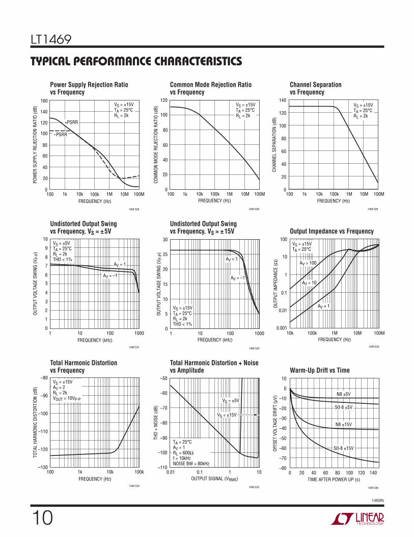
Power Supply Rejection Ratiovs Frequency
Common Mode Rejection Ratiovs Frequency
Channel Separationvs Frequency
Undistorted Output Swingvs Frequency, VS = ±5V
Undistorted Output Swingvs Frequency, VS = ±15V
Output Impedance vs Frequency
Total Harmonic Distortion vs Frequency
Total Harmonic Distortion + Noisevs Amplitude
Warm-Up Drift vs Time
FREQUENCY (Hz)100
POW
ER S
UPPL
Y RE
JECT
ION
RATI
O (d
B)
60
80
100
100k 10M
1469 G28
40
20
01k 10k 1M
120
140
160
100M
–PSRR
+PSRR
VS = ±15VTA = 25°CRL = 2k
FREQUENCY (Hz)100
0
COM
MON
MOD
E RE
JECT
ION
RATI
O (d
B)
20
40
60
80
120
1k 10k 100k 1M
1469 G29
10M 100M
100
VS = ±15VTA = 25°CRL = 2k
FREQUENCY (Hz)100
CHAN
NEL
SEPA
RATI
ON (d
B)
1k 10k 100k 1M 10M 100M
140
120
100
80
60
40
20
0
1469 G30
VS = ±15VTA = 25°CRL = 2k
FREQUENCY (kHz)1
4
OUTP
UT V
OLTA
GE S
WIN
G (V
P-P)
5
6
7
8
10 100 1000
1469 G31
3
2
1
0
9
10VS = ±5VTA = 25°CRL = 2kTHD < 1%
AV = 1
AV = –1
FREQUENCY (kHz)1
0
OUTP
UT V
OLTA
GE S
WIN
G (V
P-P)
20
25
30
10 100 1000
1469 G32
15
10
5
AV = 1
AV = –1
VS = ±15VTA = 25°CRL = 2kTHD < 1%
FREQUENCY (Hz)
0.01
OUTP
UT IM
PEDA
NCE
(Ω)
0.1
1
10
100
10k 1M 10M 100M
1469 G33
0.001100k
VS = ±15VTA = 25°C
AV = 100
AV = 10
AV = 1
FREQUENCY (Hz)100
TOTA
L HA
RMON
IC D
ISTO
RTIO
N (d
B)
1k 10k 100k
1469 G34
–80
–90
–100
–110
–120
–130
VS = ±15VAV = 2RL = 2kVOUT = 10VP-P
OUTPUT SIGNAL (VRMS)0.01
–110
THD
+ NO
ISE
(dB) –70
–60
–50
0.1 1 10
1469 G35
–80
–90
–100
VS = ±15V
VS = ±5V
TA = 25°CAV = 1RL = 600Ωf = 10kHzNOISE BW = 80kHz
TIME AFTER POWER UP (s)0 20 40 60 80 100 120 140
OFFS
ET V
OLTA
GE D
RIFT
(µV)
10
0
–10
–20
–30
–40
–50
–60
–70
–80
1469 G36
S0-8 ±15V
N8 ±5V
S0-8 ±5V
N8 ±15V
LT1469
111469fb
TYPICAL PERFORMANCE CHARACTERISTICS
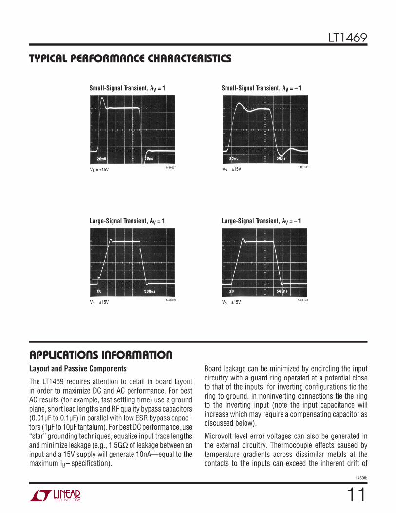
Small-Signal Transient, AV = 1
Small-Signal Transient, AV = –1
Large-Signal Transient, AV = 1
Large-Signal Transient, AV = –1
Layout and Passive Components
The LT1469 requires attention to detail in board layout in order to maximize DC and AC performance. For best AC results (for example, fast settling time) use a ground plane, short lead lengths and RF quality bypass capacitors (0.01µF to 0.1µF) in parallel with low ESR bypass capaci-tors (1µF to 10µF tantalum). For best DC performance, use “star” grounding techniques, equalize input trace lengths and minimize leakage (e.g., 1.5GΩ of leakage between an input and a 15V supply will generate 10nA—equal to the maximum IB– specification).
Board leakage can be minimized by encircling the input circuitry with a guard ring operated at a potential close to that of the inputs: for inverting configurations tie the ring to ground, in noninverting connections tie the ring to the inverting input (note the input capacitance will increase which may require a compensating capacitor as discussed below).
Microvolt level error voltages can also be generated in the external circuitry. Thermocouple effects caused by temperature gradients across dissimilar metals at the contacts to the inputs can exceed the inherent drift of
APPLICATIONS INFORMATION
VS = ±15V 1469 G37 VS = ±15V 1469 G38
VS = ±15V 1469 G39 VS = ±15V 1469 G40

LT1469
121469fb
APPLICATIONS INFORMATIONthe amplifier. Air currents over device leads should be minimized, package leads should be short and the two input leads should be as close together as possible and maintained at the same temperature.
The parallel combination of the feedback resistor and gain setting resistor on the inverting input can combine with the input capacitance to form a pole which can cause peaking or even oscillations. For feedback resistors greater than 2k, a feedback capacitor of value CF > RG • CIN/RF should be used to cancel the input pole and optimize dynamic performance. For applications where the DC noise gain is one, and a large feedback resistor is used, CF should be greater than or equal to CIN. An example would be a DAC I-to-V converter as shown on the front page of the data sheet where the DAC can have many tens of picofarads of output capacitance. Another example would be a gain of –1 with 5k resistors; a 5pF to 10pF capacitor should be added across the feedback resistor.
Input Considerations
Each input of the LT1469 is protected with a 100Ω series resistor and back-to-back diodes across the bases of the input devices. If large differential input voltages are anticipated, limit the input current to less than 10mA with an external series resistor. Each input also has two ESD clamp diodes—one to each supply. If an input is driven beyond the supply, limit the current with an external resis-tor to less than 10mA.
The LT1469 employs bias current cancellation at the inputs. The inverting input current is trimmed at zero common mode voltage to minimize errors in inverting applications such as I-to-V converters. The noninverting input current is not trimmed and has a wider variation and therefore a larger maximum value. As the input offset current can be greater than either input current, the use of balanced source resistance is NOT recommended as it actually degrades DC accuracy and also increases noise.
The input bias currents vary with common mode voltage. The cancellation circuitry was not designed to track this common mode voltage because the settling time would have been adversely affected.
The LT1469 inputs can be driven to the negative supply and to within 0.5V of the positive supply without phase reversal. As the input moves closer than 0.5V to the posi-tive supply, the output reverses phase.
Total Input Noise
The total input noise of the LT1469 is optimized for a source resistance between 1k and 20k. Within this range, the total input noise is dominated by the noise of the source resistance itself. When the source resistance is below 1k, voltage noise of the amplifier dominates. When the source resistance is above 20k, the input noise current is the dominant contributor.
Figure 1. Nulling Input Capacitance
+
–VOUT
RF
CF
CIN 1/2 LT1469
VIN
1469 F01
RG
Figure 2. Input Stage Protection
Q1+IN
1469 F02
R1100Ω Q2
–IN
R1100Ω
V–
V+

LT1469
131469fb
APPLICATIONS INFORMATIONCapacitive Loading
The LT1469 drives capacitive loads of up to 100pF in unity-gain and 300pF in a gain of –1. When there is a need to drive a larger capacitive load, a small series resistor should be inserted between the output and the load. In addition, a capacitor should be added between the output and the inverting input as shown in Figure 3.
Settling Time
The LT1469 is a single stage amplifier with an optimal thermal layout that leads to outstanding settling per-formance. Measuring settling even at the 12-bit level is very challenging, and at the 16-bit level requires a great deal of subtlety and expertise. Fortunately, there are two excellent Linear Technology reference sources for settling
measurements—Application Notes 47 and 74. Appendix B of AN47 is a vital primer on 12-bit settling measurements and AN74 extends the state-of-the-art while concentrating on settling time with a 16-bit current output DAC input.
The settling of the DAC I-to-V converter on the front page was measured using the exact methods of AN74. The optimum nulling of the DAC output capacitance requires 15pF across the 12k feedback resistor. The theoretical limit for 16-bit settling is 11.1 times this RC time constant or 2µs. The actual settling time is 2.4µs at the output of the LT1469.
The RC output noise filter adds a slight settling time delay but reduces the noise bandwidth to 1.6MHz which increases the output resolution for 16-bit accuracy.
Figure 3. Driving Capacitive Loads
+
–VOUT
RF
RO ≥ (1 + RF/RG)/(2 • CL • 5MHz)RF ≥ 10ROCF = (2RO/RF)CL
CF
1/2 LT1469
VIN
1469 F03
CL
RG
RO
LT1469
141469fb
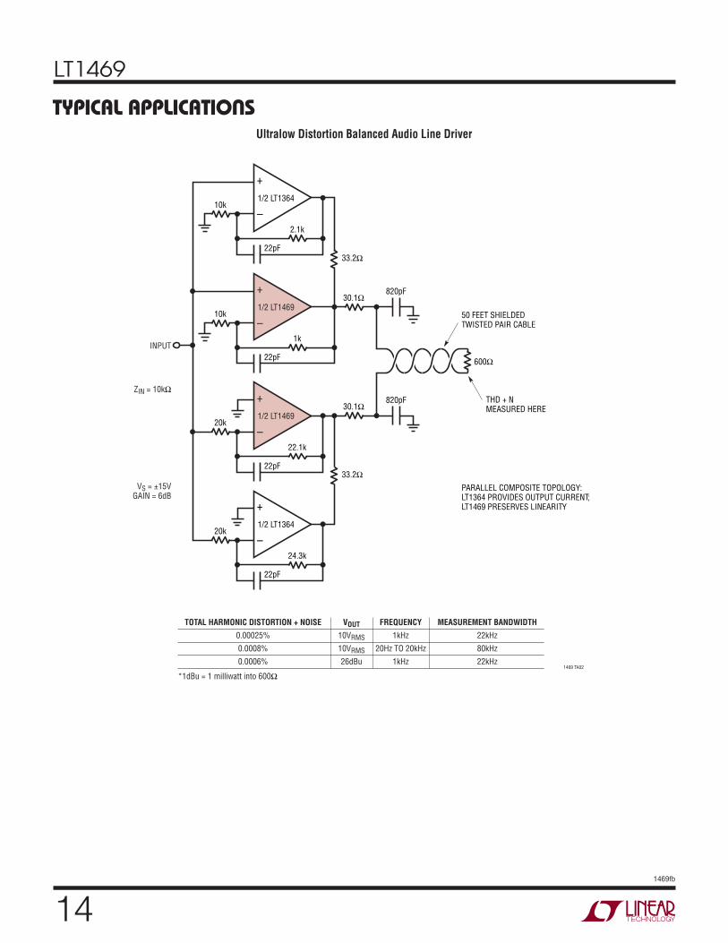
TYPICAL APPLICATIONSUltralow Distortion Balanced Audio Line Driver
+
–1/2 LT1364
10k
2.1k
22pF33.2Ω
+
–1/2 LT1469
10k
1k
22pF
+
–1/2 LT1469
20k
22.1k
22pF
820pF
50 FEET SHIELDEDTWISTED PAIR CABLE
PARALLEL COMPOSITE TOPOLOGY:LT1364 PROVIDES OUTPUT CURRENT;LT1469 PRESERVES LINEARITY
THD + NMEASURED HERE
820pF
+
–1/2 LT1364
20k
24.3k
22pF
INPUT
ZIN = 10kΩ
VS = ±15VGAIN = 6dB
1469 TA02
33.2Ω
30.1Ω
30.1Ω
600Ω
TOTAL HARMONIC DISTORTION + NOISE VOUT FREQUENCY MEASUREMENT BANDWIDTH
0.00025% 10VRMS 1kHz 22kHz
0.0008% 10VRMS 20Hz TO 20kHz 80kHz
0.0006% 26dBu 1kHz 22kHz
*1dBu = 1 milliwatt into 600Ω
LT1469
151469fb
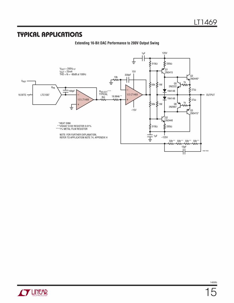
TYPICAL APPLICATIONSExtending 16-Bit DAC Performance to 200V Output Swing
–
+1/2 LT1469
15V
–15V
330pF10k
19.994k**
RSELECT***TYPICAL
6Ω
27Ω
OUTPUT
1469 TA03
27Ω
330Ω510Ω
–125V1µF
15pF
1M50k
1M50k
330Ω510Ω
125V
1N4148
1N4148
1kQ52N2222
Q62N2907
Q32N3440*
Q12N5415
Q32N5415*
1k
50k**50k**50k**50k**
Q22N3440
1µF
RFB
LTC159716 BITS
VREF
–
+1/2 LT1469
100pF
***
***
HEAT SINKVISHAY S102 RESISTOR 0.01%1% METAL FILM RESISTOR
NOTE: FOR FURTHER EXPLANATION, REFER TO APPLICATION NOTE 74, APPENDIX H
VOUT = 200VP-PIOUT = 25mATHD + N = –90dB at 100Hz

LT1469
161469fb
SIMPLIFIED SCHEMATIC
Q10
I5I2I1
I4 I6
1469 SS
I3
OUT
Q11
Q8Q9
Q7
Q6Q1 –IN+IN
V+
V–
Q5Q2
Q4 CBIASQ3

LT1469
171469fb
PACKAGE DESCRIPTION
4.00 ± 0.10(4 SIDES)
NOTE:1. DRAWING IS PROPOSED TO BE MADE A JEDEC PACKAGE OUTLINE MO-220 VARIATION (WGGD-X)—TO BE APPROVED2. DRAWING NOT TO SCALE3. ALL DIMENSIONS ARE IN MILLIMETERS4. DIMENSIONS OF EXPOSED PAD ON BOTTOM OF PACKAGE DO NOT INCLUDE MOLD FLASH. MOLD FLASH, IF PRESENT, SHALL NOT EXCEED 0.15mm ON ANY SIDE5. EXPOSED PAD SHALL BE SOLDER PLATED6. SHADED AREA IS ONLY A REFERENCE FOR PIN 1 LOCATION ON THE TOP AND BOTTOM OF PACKAGE
PIN 1TOP MARK(NOTE 6)
0.40 ± 0.10
16
127
BOTTOM VIEW—EXPOSED PAD
2.65 ± 0.10
0.75 ± 0.05
R = 0.115TYP
0.25 ± 0.050.50 BSC
2.50 REF
3.38 ±0.10
0.200 REF
0.00 – 0.05
(DF12) DFN 0806 REV Ø
RECOMMENDED SOLDER PAD PITCH AND DIMENSIONSAPPLY SOLDER MASK TO AREAS THAT ARE NOT SOLDERED
0.70 ±0.05
0.25 ±0.050.50 BSC
3.10 ± 0.05
4.50 ± 0.05
PACKAGE OUTLINE
PIN 1 NOTCHR = 0.20 TYP OR0.35 × 45°CHAMFER
2.65 ± 0.05
3.38 ±0.05
2.50 REF
DF Package12-Lead Plastic DFN (4mm × 4mm)
(Reference LTC DWG # 05-08-1733 Rev Ø)

LT1469
181469fb
PACKAGE DESCRIPTIONN8 Package
8-Lead PDIP (Narrow 0.300)(Reference LTC DWG # 05-08-1510)
S8 Package8-Lead Plastic Small Outline (Narrow 0.150)
(Reference LTC DWG # 05-08-1610)
N8 1002
.065(1.651)
TYP
.045 – .065(1.143 – 1.651)
.130 ± .005(3.302 ± 0.127)
.020(0.508)
MIN.018 ± .003(0.457 ± 0.076)
.120(3.048)
MIN
1 2 3 4
8 7 6 5
.255 ± .015*(6.477 ± 0.381)
.400*(10.160)
MAX
.008 – .015(0.203 – 0.381)
.300 – .325(7.620 – 8.255)
.325+.035–.015+0.889–0.3818.255( )
NOTE:1. DIMENSIONS ARE
INCHESMILLIMETERS
*THESE DIMENSIONS DO NOT INCLUDE MOLD FLASH OR PROTRUSIONS. MOLD FLASH OR PROTRUSIONS SHALL NOT EXCEED .010 INCH (0.254mm)
.100(2.54)BSC
.016 – .050(0.406 – 1.270)
.010 – .020(0.254 – 0.508)
× 45°
0°– 8° TYP.008 – .010
(0.203 – 0.254)
SO8 0303
.053 – .069(1.346 – 1.752)
.014 – .019(0.355 – 0.483)
TYP
.004 – .010(0.101 – 0.254)
.050(1.270)
BSC
1 2 3 4
.150 – .157(3.810 – 3.988)
NOTE 3
8 7 6 5
.189 – .197(4.801 – 5.004)
NOTE 3
.228 – .244(5.791 – 6.197)
.245MIN .160 ±.005
RECOMMENDED SOLDER PAD LAYOUT
.045 ±.005 .050 BSC
.030 ±.005 TYP
INCHES(MILLIMETERS)
NOTE:1. DIMENSIONS IN
2. DRAWING NOT TO SCALE3. THESE DIMENSIONS DO NOT INCLUDE MOLD FLASH OR PROTRUSIONS. MOLD FLASH OR PROTRUSIONS SHALL NOT EXCEED .006" (0.15mm)

LT1469
191469fb
Information furnished by Linear Technology Corporation is believed to be accurate and reliable. However, no responsibility is assumed for its use. Linear Technology Corporation makes no representa-tion that the interconnection of its circuits as described herein will not infringe on existing patent rights.
REVISION HISTORYREV DATE DESCRIPTION PAGE NUMBER
B 1/11 Change to Electrical Characteristics 3, 5, 6
(Revision history begins at Rev B)
LT1469
201469fb
Linear Technology Corporation1630 McCarthy Blvd., Milpitas, CA 95035-7417 (408) 432-1900 FAX: (408) 434-0507 www.linear.com LINEAR TECHNOLOGY CORPORATION 2000
LT 0111 REV B • PRINTED IN USA
RELATED PARTS
TYPICAL APPLICATION
PART NUMBER DESCRIPTION COMMENTS
LT1167 Precision Instrumentation Amplifier Single Resistor Gain Set, 0.04% Max Gain Error, 10ppm Max Gain Nonlinearity
LT1468 Single 90MHz, 22V/µs, 16-Bit Accurate Op Amp 75µV VOS(MAX), Single Version of LT1469
LT1468-2 Single 200MHz, 30V/µs, 16-Bit Accurate AV ≥ 2 Op Amp 75µV VOS(MAX)
LT1469-2 Dual 200MHz, 30V/µs, 16-Bit Accurate AV ≥ 2 Op Amp 75µV VOS(MAX)
LTC1595/LTC1596 16-Bit Serial Multiplying IOUT DAC ±1LSB Max INL/DNL, Low Glitch, DAC8043 16-Bit Upgrade
LTC1597 16-Bit Parallel Multiplying IOUT DAC ±1LSB Max INL/DNL, Low Glitch, On-Chip Bipolar Resistors
LTC1604 16-Bit, 333ksps Sampling ADC ±2.5V Input, SINAD = 90dB, THD = –100dB
LTC1605 Single 5V, 16-Bit, 100ksps Sampling ADC Low Power, ±10V Inputs, Parallel/Byte Interface
LT1723 Dual 200MHz, 70V/µs Low Noise Precision Op Amp VS ≤ ±5V, en = 3.8nV/√Hz, –85dBc at 1MHz
LT1801 Dual 80MHz, 25V/µs Low Power Rail-to-Rail Precision Op Amp
VS ≤ ±5V, ICC = 1.6mA, VOS ≤ 350µV
LT6221 Dual 60MHz, 20V/µs Low Power Rail-to-Rail Precision Op Amp
VS ≤ ±5V, ICC = 0.9mA, VOS ≤ 350µV
LTC6244HV Dual 50MHz, Low Noise, Precision CMOS Op Amp VS ≤ ±5V, VOS ≤ 100µV, IB ≤ 75pA
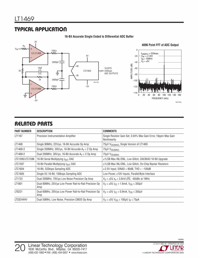
16-Bit Accurate Single Ended to Differential ADC Buffer
–
+
+
–
2k
VIN
2k
–5V
–5V
5V
5V
RS
10pF
100Ω
100Ω
3000pF
3000pF
+IN
LTC1604
1/2 LT1469
1/2 LT1469
16 BITS333kspsADC OUTPUTS
1469 TA04
–IN
FREQUENCY (kHz)0
1469 TA04a
20 40 60 80 100 120 140 160
AMPL
ITUD
E (d
B)
0
–20
–40
–60
–80
–100
–120
–140
fSAMPLE = 333kspsVIN = ±1.25VfIN = 100kHzVS = ±5V
4096 Point FFT of ADC Output