Embed Size (px)
Citation preview
LT3724
13724fd
TYPICAL APPLICATION
FEATURES
APPLICATIONS
DESCRIPTION
High Voltage, Current Mode Switching Regulator Controller
The LT®3724 is a DC/DC controller used for medium power, low part count, low cost, high efficiency supplies. It of-fers a wide 4V-60V input range (7.5V minimum startup voltage) and can implement step-down, step-up, inverting and SEPIC topologies.
The LT3724 includes Burst Mode operation, which re-duces quiescent current below 100µA and maintains high efficiency at light loads. An internal high voltage bias regulator allows for simple biasing and can be back driven to increase efficiency.
Additional features include fixed frequency current mode control for fast line and load transient response; a gate driver capable of driving large N-channel MOSFETs; a precision undervoltage lockout function; 10µA shutdown current; short-circuit protection; and a programmable soft-start function that directly controls output voltage slew rates at startup which limits inrush current, minimizes overshoot and facilitates supply sequencing.
High Voltage Step-Down Regulator
n Wide Input Range: 4V to 60Vn Output Voltages up to 36V (Step-Down)n Burst Mode® Operation: <100µA Supply Currentn 10µA Shutdown Supply Currentn ±1.3% Reference Accuracyn 200kHz Fixed Frequencyn Drives N-Channel MOSFETn Programmable Soft-Startn Programmable Undervoltage Lockoutn Internal High Voltage Regulator for Gate Driven Thermal Shutdownn Current Limit Unaffected by Duty Cyclen 16-Pin Thermally Enhanced TSSOP Package
n Industrial Power Distributionn 12V and 42V Automotive and Heavy Equipmentn High Voltage Single Board Systemsn Distributed Power Systemsn Avionicsn Telecom Power
Efficiency and Power Loss vs Load Current
VIN
SHDN
CSS
Burst_EN
VFB
VC
SGND
BOOST
TG
SW
VCC
PGND
SENSE+
SENSE–
VIN30V TO
60V
VOUT24V75W
3724 TA01a
LT37241M
68.1k
1000pF
4.99k 93.1k
10Ω
200k
0.22µF
COUT330µF
CIN68µF
1µF
47µH
0.025ΩSi7852
SS3H9
120pF680pF
40.2k
+
LOAD CURRENT (A)0.1
EFFI
CIEN
CY (%
)
POWER LOSS (W
)
95
90
85
80
75
70
65
12
10
8
6
4
2
01 10
3724 TA01b
VIN = 48V
LOSS
EFFICIENCY
L, LT, LTC, LTM, Linear Technology and the Linear logo are registered trademarks and Burst Mode is a trademark of Linear Technology Corporation. All other trademarks are the property of their respective owners. Protected by U.S. Patents including 5731694, 6498466, 6611131.
LT3724
23724fd
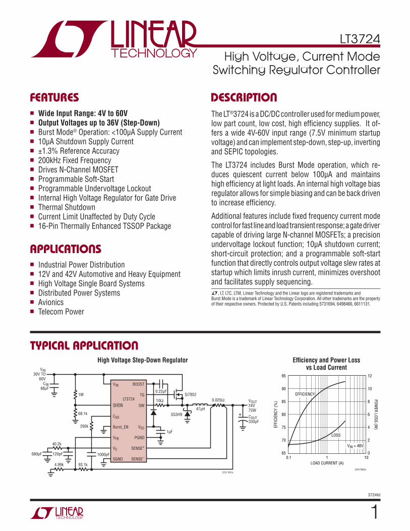
PIN CONFIGURATIONABSOLUTE MAXIMUM RATINGS
Input Supply Voltage (VIN) ......................... 65V to –0.3VBoosted Supply Voltage (BOOST) .............. 80V to –0.3VSwitch Voltage (SW)(Note 8) ........................ 65V to –1VDifferential Boost Voltage
(BOOST to SW) ...................................... 24V to –0.3VBias Supply Voltage (VCC) .......................... 24V to –0.3VSENSE+ and SENSE– Voltages ................... 40V to –0.3V
(SENSE+ to SENSE–) ................................... 1V to –1VBURST_EN Voltage .................................... 24V to –0.3VVC, VFB, CSS, and SHDN Voltages................. 5V to –0.3VCSS and SHDN Pin Currents .....................................1mAOperating Junction Temperature Range (Notes 2, 3)
LT3724E ............................................. –40°C to 125°C LT3724I .............................................. –40°C to 125°C LT3724MP.......................................... –55°C to 125°C
Storage Temperature .............................. –65°C to 150°CLead Temperature (Soldering, 10 sec) .................. 300°C
(Note 1)
FE PACKAGE16-LEAD PLASTIC TSSOP
1
2
3
4
5
6
7
8
TOP VIEW
16
15
14
13
12
11
10
9
VIN
NC
SHDN
CSS
BURST_EN
VFB
VC
SGND
BOOST
TG
SW
NC
VCC
PGND
SENSE+
SENSE–
17
TJMAX = 125°C, θJA = 40°C/W, θJC = 10°C/W
EXPOSED PAD IS SGND (PIN 17), MUST BE SOLDERED TO PCB
ELECTRICAL CHARACTERISTICS
ORDER INFORMATIONLEAD FREE FINISH TAPE AND REEL PART MARKING PACKAGE DESCRIPTION TEMPERATURE RANGE
LT3724EFE#PBF LT3724EFE#TRPBF 3724EFE 16-Lead Plastic TSSOP –40°C to 125°C
LT3724IFE#PBF LT3724IFE#TRPBF 3724IFE 16-Lead Plastic TSSOP –40°C to 125°C
LEAD BASED FINISH TAPE AND REEL PART MARKING* PACKAGE DESCRIPTION TEMPERATURE RANGE
LT3724MPFE LT3724MPFE#TR 3724MPFE 16-Lead Plastic TSSOP –55°C to 125°C
Consult LTC Marketing for parts specified with wider operating temperature ranges. Consult LTC Marketing for information on non-standard lead based finish parts.For more information on lead free part marking, go to: http://www.linear.com/leadfree/ For more information on tape and reel specifications, go to: http://www.linear.com/tapeandreel/
The l denotes the specifications which apply over the full operating temperature range, otherwise specifications are at TA = 25°C. VIN = 20V, VCC = BOOST = BURST_EN = 10V, SHDN = 2V, SENSE– = SENSE+ = 10V, SGND = PGND = SW = 0V, unless otherwise noted.
SYMBOL PARAMETER CONDITIONS MIN TYP MAX UNITS
VIN Operating Voltage Range (Note 4) Minimum Start Voltage UVLO Threshold (Falling) UVLO Threshold Hysteresis
l
l
l
4 7.5
3.65
3.8 670
60
3.95
V V V
mV
IVIN VIN Supply Current VIN Burst Mode Current VIN Shutdown Current
VCC > 9V VBURST_EN = 0V, VFB = 1.35V VSHDN = 0V
20 20 10
15
µA µA µA
LT3724
33724fd
ELECTRICAL CHARACTERISTICS The l denotes the specifications which apply over the full operating temperature range, otherwise specifications are at TA = 25°C. VIN = 20V, VCC = BOOST = BURST_EN = 10V, SHDN = 2V, SENSE– = SENSE+ = 10V, SGND = PGND = SW = 0V, unless otherwise noted.
SYMBOL PARAMETER CONDITIONS MIN TYP MAX UNITS
VBOOST Operating Voltage Range Operating Voltage Range (Note 5) UVLO Threshold (Rising) UVLO Threshold Hysteresis
VBOOST - VSW VBOOST - VSW VBOOST - VSW
l
l
5
400
75 20
V V V
mV
IBOOST BOOST Supply Current (Note 6) BOOST Burst Mode Current BOOST Shutdown Current
VBURST_EN = 0V VSHDN = 0V
1.4 0.1 0.1
mA µA µA
VCC Operating Voltage Range (Note 5) Output Voltage UVLO Threshold (Rising) UVLO Threshold Hysteresis
Over Full Line and Load Range
l
l
8
6.25 500
20 8.3
V V V
mV
IVCC VCC Supply Current (Note 6) VCC Burst Mode Current VCC Shutdown Current Short-Circuit Current
VBURST_EN = 0V VSHDN = 0V
l
l
–30
1.7 80 20
–55
2.1 mA µA µA
mA
VFB Error Amp Reference Voltage Measured at VFB Pin l
1.224 1.215
1.231 1.238 1.245
V V
IFB Feedback Input Current 25 nA
VSHDN Enable Threshold (Rising) Threshold Hysteresis
l 1.3 1.35 120
1.4 V mV
VSENSE Common Mode Range Current Limit Sense Voltage
VSENSE
+ – VSENSE–
l
l
0 140
150
36 175
V mV
ISENSE Input Current (ISENSE
+ + ISENSE–)
VSENSE(CM) = 0V VSENSE(CM) = 2.5V VSENSE(CM) > 4V
400 2
–150
µA µA µA
fSW Operating Frequency MP Grade
l
l
190 175 165
200
200
210 220 225
kHz kHz kHz
VFB(SS) Soft-Start Disable Voltage Soft-Start Disable Hysteresis
VFB Rising 1.185 300
V mV
ISS Soft-Start Capacitor Control Current 2 µA
gm Error Amp Transconductance l 275 340 400 µmhos
AV Error Amp DC Voltage Gain 62 dB
VC Error Amp Output Range Zero Current to Current Limit 1.2 V
IVC Error Amp Sink/Source Current ±30 µA
VTG Gate Drive Output On Voltage (Note 7) Gate Drive Output Off Voltage
CLOAD = 3300pF CLOAD = 3300pF
9.8 0.1
V V
tTG Gate Drive Rise/Fall Time 10% to 90% or 90% to 10%, CLOAD = 3300pF 60 ns
tTG(OFF) Minimum Switch Off Time 350 ns
tTG(ON) Minimum Switch On Time l 300 500 ns
ISW SW Pin Sink Current VSW = 2V 300 mA
LT3724
43724fd
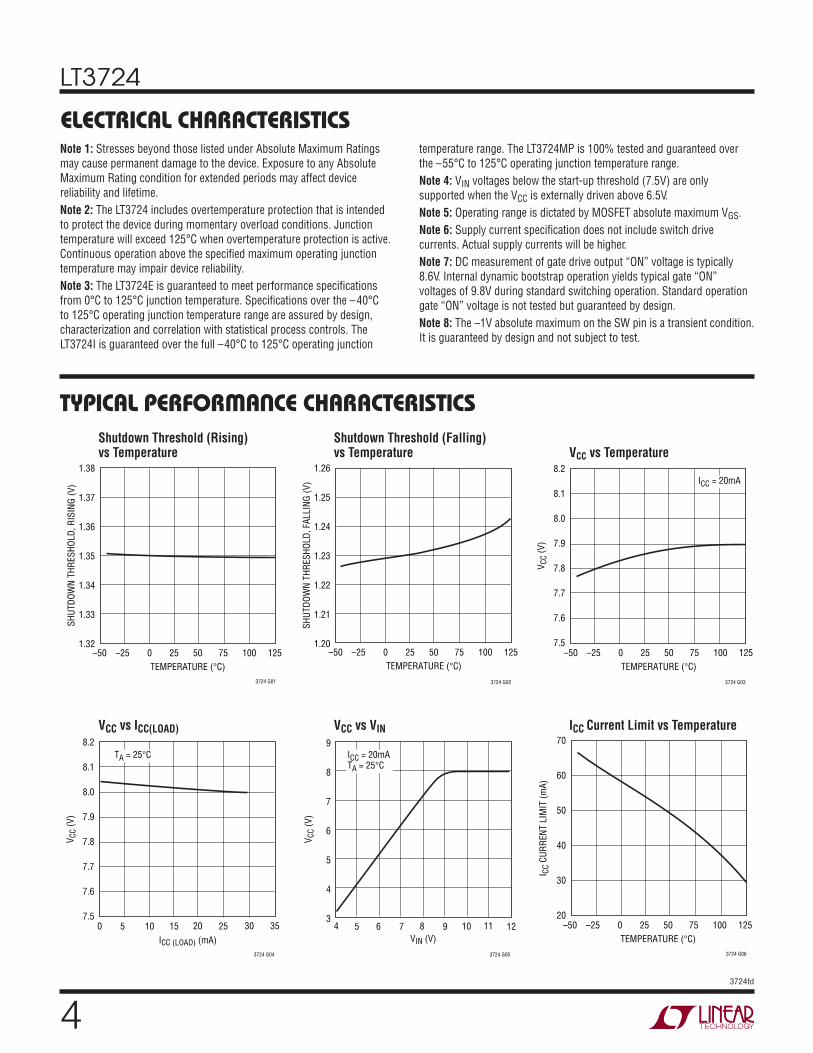
TYPICAL PERFORMANCE CHARACTERISTICSShutdown Threshold (Rising) vs Temperature
Shutdown Threshold (Falling)vs Temperature
V CC vs Temperature
VCC vs ICC(LOAD)
VCC vs VIN
ICC Current Limit vs Temperature
3724 G01
SHUT
DOW
N TH
RESH
OLD,
RIS
ING
(V)
1.38
1.37
1.36
1.35
1.34
1.33
1.32
TEMPERATURE (°C)–50 25 75–25 0 50 100 125
3724 G02
TEMPERATURE (°C)–50
SHUT
DOW
N TH
RESH
OLD,
FAL
LING
(V)
1.26
1.25
1.24
1.23
1.22
1.21
1.2025 75–25 0 50 100 125
TEMPERATURE (°C)–50 25 75–25 0 50 100 125
3724 G03
8.2
8.1
8.0
7.9
7.8
7.7
7.6
7.5
V CC
(V)
ICC = 20mA
3724 G04
ICC (LOAD) (mA)0
8.2
8.1
8.0
7.9
7.8
7.7
7.6
7.515 255 10 20 30 35
V CC
(V)
TA = 25°C
3724 G05
VIN (V)
V CC
(V)
9
8
7
6
5
4
34 6 8 95 7 10 11 12
ICC = 20mATA = 25°C
TEMPERATURE (°C)–50 25 75–25 0 50 100 125
3724 G06
I CC
CURR
ENT
LIM
IT (m
A)
70
60
50
40
30
20
Note 1: Stresses beyond those listed under Absolute Maximum Ratings may cause permanent damage to the device. Exposure to any Absolute Maximum Rating condition for extended periods may affect device reliability and lifetime.Note 2: The LT3724 includes overtemperature protection that is intended to protect the device during momentary overload conditions. Junction temperature will exceed 125°C when overtemperature protection is active. Continuous operation above the specified maximum operating junction temperature may impair device reliability.Note 3: The LT3724E is guaranteed to meet performance specifications from 0°C to 125°C junction temperature. Specifications over the –40°C to 125°C operating junction temperature range are assured by design, characterization and correlation with statistical process controls. The LT3724I is guaranteed over the full –40°C to 125°C operating junction
temperature range. The LT3724MP is 100% tested and guaranteed over the –55°C to 125°C operating junction temperature range.Note 4: VIN voltages below the start-up threshold (7.5V) are only supported when the VCC is externally driven above 6.5V.Note 5: Operating range is dictated by MOSFET absolute maximum VGS.Note 6: Supply current specification does not include switch drive currents. Actual supply currents will be higher.Note 7: DC measurement of gate drive output “ON” voltage is typically 8.6V. Internal dynamic bootstrap operation yields typical gate “ON” voltages of 9.8V during standard switching operation. Standard operation gate “ON” voltage is not tested but guaranteed by design.Note 8: The –1V absolute maximum on the SW pin is a transient condition. It is guaranteed by design and not subject to test.
ELECTRICAL CHARACTERISTICS
LT3724
53724fd
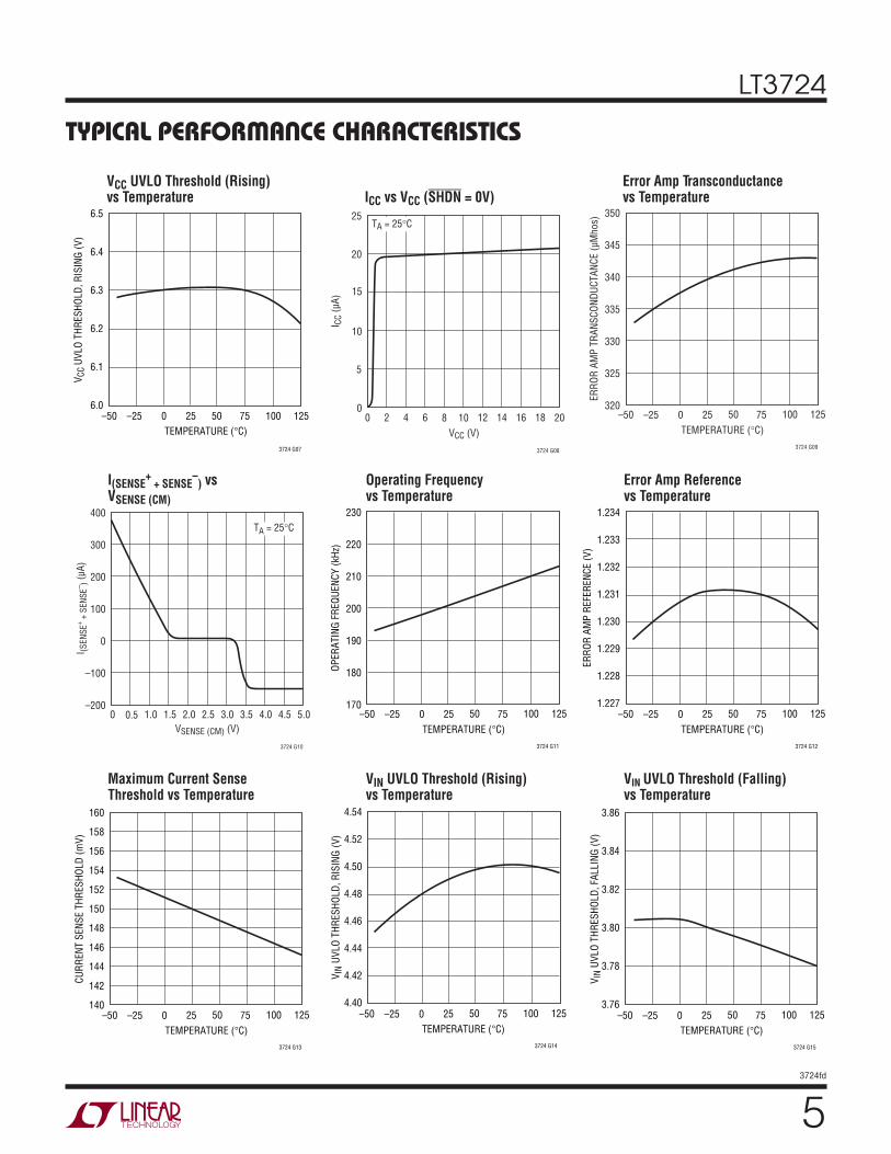
VCC UVLO Threshold (Rising)vs Temperature
ICC vs VCC (SHDN = 0V)
Error Amp Transconductance vs Temperature
TYPICAL PERFORMANCE CHARACTERISTICS
I(SENSE+
+ SENSE–
) vs VSENSE (CM)
Operating Frequency vs Temperature
Error Amp Referencevs Temperature
Maximum Current Sense Threshold vs Temperature
VIN UVLO Threshold (Rising)vs Temperature
V IN UVLO Threshold (Falling)vs Temperature
3724 G07
TEMPERATURE (°C)–50 25 75–25 0 50 100 125
V CC
UVLO
THR
ESHO
LD, R
ISIN
G (V
)
6.5
6.4
6.3
6.2
6.1
6.0
3724 G08
VCC (V)0
I CC
(µA)
15
20
25
16
10
5
02 4 6 8 10 12 14 18 20
TA = 25°C
TEMPERATURE (°C)–50
ERRO
R AM
P TR
ANSC
ONDU
CTAN
CE (µ
Mho
s)
350
345
340
335
330
325
32025 75
3724 G09
–25 0 50 100 125
VSENSE (CM) (V)0
I (SEN
SE+ +
SEN
SE– ) (
µA)
400
300
200
100
0
–100
–2000.5 1.0 1.5 2.0
3724 G10
2.5 4.53.5 5.04.03.0
TA = 25°C
TEMPERATURE (°C)–50
OPER
ATIN
G FR
EQUE
NCY
(kHz
)
230
220
210
200
190
180
17025 75
3724 G11
–25 0 50 100 125TEMPERATURE (°C)
–50 25 75
3724 G12
–25 0 50 100 125
1.234
1.233
1.232
1.231
1.230
1.229
1.228
1.227
ERRO
R AM
P RE
FERE
NCE
(V)
TEMPERATURE (°C)–50 25 75–25 0 50 100 125
CURR
ENT
SENS
E TH
RESH
OLD
(mV)
160
158
156
154
152
150
148
146
144
142
140
3724 G13
TEMPERATURE (°C)–50 25 75–25 0 50 100 125
3724 G14
4.54
4.52
4.50
4.48
4.46
4.44
4.42
4.40
V IN
UVLO
THR
ESHO
LD, R
ISIN
G (V
)
TEMPERATURE (°C)–50 25 75–25 0 50 100 125
3724 G15
V IN
UVLO
THR
ESHO
LD, F
ALLI
NG (V
)
3.86
3.84
3.82
3.80
3.78
3.76
LT3724
63724fd
PIN FUNCTIONSVIN (Pin 1): The VIN pin is the main supply pin and should be decoupled to SGND with a low ESR capacitor located close to the pin.
NC (Pin 2): No Connection.
SHDN (Pin 3): The SHDN pin has a precision IC enable threshold of 1.35V (rising) with 120mV of hysteresis. It is used to implement an undervoltage lockout (UVLO) circuit. See Application Information section for implementing a UVLO function. When the SHDN pin is pulled below a transistor VBE (0.7V), a low current shutdown mode is entered, all internal circuitry is disabled and the VIN sup-ply current is reduced to approximately 10µA. Typical pin input bias current is <10µA and the pin is internally clamped to 6V.
CSS (Pin 4): The soft-start pin is used to program the sup-ply soft-start function. The pin is connected to VOUT via a ceramic capacitor (CSS) and 200kΩ series resistor. During start-up, the supply output voltage slew rate is controlled to produce a 2µA average current through the soft-start coupling capacitor. Use the following formula to calculate CSS for a given output voltage slew rate:
CSS = 2µA(tSS/VOUT)
See the application section for more information on setting the rise time of the output voltage during start-up. Shorting this pin to SGND disables the soft-start function.
BURST_EN (Pin 5): The BURST_EN pin is used to enable or disable Burst Mode operation. Connect the BURST_EN pin to ground to enable the burst mode function. Connect the pin to VCC to disable the burst mode function.
VFB (Pin 6): The output voltage feedback pin, VFB, is externally connected to the supply output voltage via a resistive divider. The VFB pin is internally connected to the inverting input of the error amplifier. In regulation, VFB is 1.231V.
VC (Pin 7): The VC pin is the output of the error amplifier whose voltage corresponds to the maximum (peak) switch current per oscillator cycle. The error amplifier is typically configured as an integrator circuit by connecting an RC network from the VC pin to SGND. This circuit creates the dominant pole for the converter regulation control loop. Specific integrator characteristics can be configured to optimize transient response. Connecting a 100pF or greater high frequency bypass capacitor from this pin to ground is recommended. When Burst Mode operation is enabled (see Pin 5 description), an internal low impedance clamp on the VC pin is set at 100mV below the burst threshold, which limits the negative excursion of the pin voltage. Therefore, this pin cannot be pulled low with a low imped-ance source. If the VC pin must be externally manipulated, do so through a 1kΩ series resistance.
SGND (Pin 8, 17): The SGND pin is the low noise ground reference. It should be connected to the –VOUT side of the output capacitors. Careful layout of the PCB is necessary to keep high currents away from this SGND connection. See the Application Information section for helpful hints on PCB layout of grounds.
SENSE– (Pin 9): The SENSE– pin is the negative input for the current sense amplifier and is connected to the VOUT side of the sense resistor for step-down applications. The sensed inductor current limit is set to 150mV across the SENSE inputs.
SENSE+ (Pin 10): The SENSE+ pin is the positive input for the current sense amplifier and is connected to the induc-tor side of the sense resistor for step-down applications. The sensed inductor current limit is set to 150mV across the SENSE inputs.
PGND (Pin 11): The PGND pin is the high-current ground reference for internal low side switch and the VCC regulator circuit. Connect the pin directly to the negative terminal of the VCC decoupling capacitor. See the Application Informa-tion section for helpful hints on PCB layout of grounds.
LT3724
73724fd
PIN FUNCTIONSVCC (Pin 12): The VCC pin is the internal bias supply decoupling node. Use a low ESR 1µF ceramic capacitor to decouple this node to PGND. Most internal IC func-tions are powered from this bias supply. An external diode connected from VCC to the BOOST pin charges the bootstrapped capacitor during the off-time of the main power switch. Back driving the VCC pin from an external DC voltage source, such as the VOUT output of the buck regulator supply, increases overall efficiency and reduces power dissipation in the IC. In shutdown mode this pin sinks 20µA until the pin voltage is discharged to 0V.
NC (Pin 13): No Connection.
SW (Pin 14): In step-down applications the SW pin is connected to the cathode of an external clamping Schottky diode, the source of the power MOSFET and the induc-tor. The SW node voltage swing is from VIN during the on-time of the power MOSFET, to a Schottky voltage drop below ground during the off-time of the power MOSFET. In start-up and in operating modes where there is insuf-ficient inductor current to freewheel the Schottky diode, an internal switch is turned on to pull the SW pin to ground
so that the BOOST pin capacitor can be charged. Give careful consideration in choosing the Schottky diode to limit the negative voltage swing on the SW pin.
TG (Pin 15): The TG pin is the bootstrapped gate drive for the top N-Channel MOSFET. Since very fast high cur-rents are driven from this pin, connect it to the gate of the power MOSFET with a short and wide, typically 0.02” width, PCB trace to minimize inductance.
BOOST (Pin 16): The BOOST pin is the supply for the bootstrapped gate drive and is externally connected to a low ESR ceramic boost capacitor referenced to SW pin. The recommended value of the BOOST capacitor, CBOOST, is 50 times greater than the total input capacitance of the topside MOSFET. In most applications 0.1µF is adequate. The maximum voltage that this pin sees is VIN + VCC, ground referred.
Exposed Pad (SGND) (Pin 17): The exposed leadframe is internally connected to the SGND pin. Solder the exposed pad to the PCB ground for electrical contact and optimal thermal performance.
LT3724
83724fd
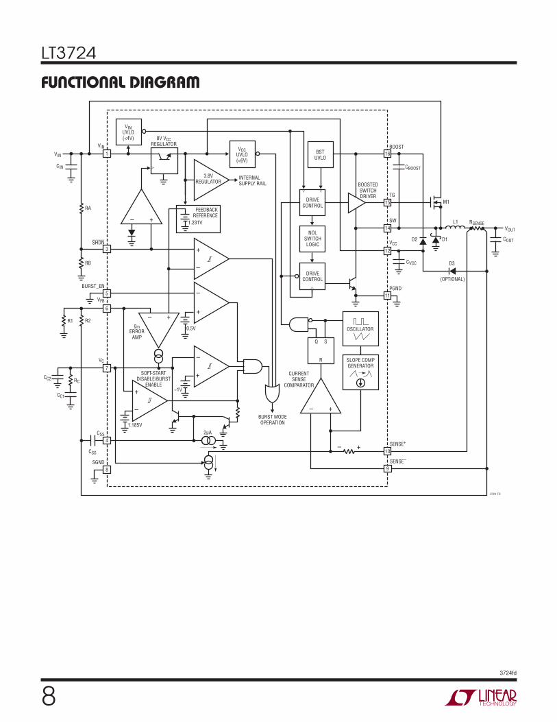
FUNCTIONAL DIAGRAM
– +
– +
– +
–
+
–
+
VINUVLO(<4V)
BSTUVLO
8V VCCREGULATOR
FEEDBACKREFERENCE
–
+
1.231V
3.8VREGULATOR
INTERNALSUPPLY RAIL
1
8
7
VIN VCCUVLO(<6V)
SHDN
DRIVECONTROL
NOLSWITCHLOGIC
DRIVECONTROL
BURST_EN
VC
CSS
SENSE–
VFB
–
+
1.185V
~1V
0.5V
2µA
BURST MODEOPERATION
SOFT-STARTDISABLE/BURST
ENABLE
R
SQ
OSCILLATOR
SLOPE COMPGENERATOR
BOOST
TGM1
D2
D3
D1
L1
(OPTIONAL)
RSENSESW
VCC
PGND
SENSE+
SGND
3724 FD
BOOSTEDSWITCHDRIVER
CURRENTSENSE
COMPARATOR
gmERROR
AMP
11
12
14
9
10
6
4
CC2
CC1
R1
RA
RB
VIN
CIN
R2
CSS
5
3
16
15
CBOOST
VOUT
COUT
CVCC
– +
RC

LT3724
93724fd
OPERATIONSThe LT3724 is a PWM controller with a constant frequency, current mode control architecture. It is designed for low to medium power, switching regulator applications. Its high operating voltage capability allows it to step-up or down input voltages up to 60V without the need for a transformer. The LT3724 is used in nonsynchronous applications, meaning that a freewheeling rectifier diode (D1 of Function Diagram) is used instead of a bottom side MOSFET. For circuit operation, please refer to the Functional Diagram of the IC and Typical Application on the front page of the data sheet. The LT3800 is a similar part that uses synchronous rectification, replacing the diode with a MOSFET in a step-down application.
Main Control Loop
During normal operation, the external N-channel MOSFET switch is turned on at the beginning of each cycle. The switch stays on until the current in the inductor exceeds a current threshold set by the DC control voltage, VC, the output of the voltage control loop. The voltage control loop monitors the output voltage, via the VFB pin voltage, and compares it to an internal 1.231V reference. It increases the current threshold when the VFB voltage is below the reference voltage and decreases the current threshold when the VFB voltage is above the reference voltage. For instance, when an increase in the load current occurs, the output voltage drops causing the VFB voltage to drop relative to the 1.231V reference. The voltage control loop senses the drop and increases the current threshold. The peak inductor current is increased until the average induc-tor current equals the new load current and the output voltage returns to regulation.
Current Limit/Short-Circuit
The inductor current is measured with a series sense resistor (see the Typical Application on the front page). When the voltage across the sense resistor reaches the maximum current sense threshold, typically 150mV, the TG MOSFET driver is disabled for the remainder of that cycle. If the maximum current sense threshold is still ex-ceeded at the beginning of the next cycle, the entire cycle is skipped. Cycle skipping keeps the inductor currents to a controlled value during a short-circuit, particularly when VIN is high. Setting the sense resistor value is discussed in the “Application Information” section.
VCC/Boosted Supply
An internal VCC regulator provides VIN derived gate-drive power for start-up under all operating conditions with MOSFET gate charge loads up to 90nC. The regulator can operate continuously in applications with VIN voltages up to 60V, provided the VIN voltage and/or MOSFET gate charge currents do not create excessive power dissipa-tion in the IC. Safe operating conditions for continuous regulator use are shown in Figure 1. In applications where these conditions are exceeded, VCC must be derived from an external source after start-up. The LT3724 regulator can, however, be used for “full time” use in applications where short-duration VIN transients exceed allowable continuous voltages.
For higher converter efficiency and less power dissipa-tion in the IC, VCC can also be supplied from an external supply such as the converter output. When an external supply back drives the internal VCC regulator through an external diode and the VCC voltage is pulled to a diode above its regulation voltage, the internal regulator is dis-abled and goes into a low current mode. VCC is the bias supply for most of the internal IC functions and is also used to charge the bootstrapped capacitor (CBOOST) via an external diode. The external MOSFET switch is biased from the bootstrapped capacitor. While the external MOSFET switch is off, an internal BJT switch, whose collector is connected to the SW pin and emitter is connected to the PGND pin, is turned on to pull the SW node to PGND and recharge the bootstrap capacitor. The switch stays on until
Figure 1. VCC Regulator Continuous Operating Conditions
MOSFET TOTAL GATE CHARGE (nC)0
V IN
(V)
70
60
50
40
30
20
1020 40 60 80
3724 F01
100
SAFEOPERATING
AREA
(Refer to Functional Diagram)
LT3724
103724fd
OPERATIONSeither the start of the next cycle or until the bootstrapped capacitor is fully charged.
MOSFET Driver
The LT3724 contains a high speed boosted driver to turn on and off an external N-channel MOSFET switch. The MOSFET driver derives its power from the boost capacitor which is referenced to the SW pin and the source of the MOSFET. The driver provides a large pulse of current to turn on the MOSFET fast and minimize transition times. Multiple MOSFETs can be paralleled for higher current operation.
To eliminate the possibility of shoot through between the MOSFET and the internal SW pull-down switch, an adap-tive nonoverlap circuit ensures that the internal pull-down switch does not turn on until the gate of the MOSFET is below its turn on threshold.
Low Current Operation (Burst Mode Operation)
To increase low current load efficiency, the LT3724 is capable of operating in Linear Technology’s proprietary Burst Mode operation where the external MOSFET operates intermittently based on load current demand. The Burst Mode function is disabled by connecting the BURST_EN pin to VCC and enabled by connecting the pin to SGND.
When the required switch current, sensed via the VC pin voltage, is below 15% of maximum, Burst Mode operation is employed and that level of sense current is latched onto the IC control path. If the output load requires less than this latched current level, the converter will overdrive the output slightly during each switch cycle. This overdrive condition is sensed internally and forces the voltage on the VC pin to continue to drop. When the voltage on VC drops 150mV below the 15% load level, switching is disabled, and the LT3724 shuts down most of its internal circuitry, reducing total quiescent current to 100µA. When the converter output begins to fall, the VC pin voltage begins to climb. When the voltage on the VC pin climbs back to the 15% load level, the IC returns to normal operation and
switching resumes. An internal clamp on the VC pin is set at 100mV below the output disable threshold, which limits the negative excursion of the pin voltage, minimizing the converter output ripple during Burst Mode operation.
During Burst Mode operation, the VIN pin current is 20µA and the VCC current is reduced to 80µA. If no external drive is provided for VCC, all VCC bias currents originate from the VIN pin, giving a total VIN current of 100µA. Burst current can be reduced further when VCC is driven using an output derived source, as the VCC component of VIN current is then reduced by the converter duty cycle ratio.
Start-Up
The following section describes the start-up of the supply and operation down to 4V once the step-down supply is up and running. For the protection of the LT3724 and the switching supply, there are internal undervoltage lockout (UVLO) circuits with hysteresis on VIN, VCC and VBOOST, as shown in the Electrical Characteristics table. Start-up and continuous operation require that all three of these undervoltage lockout conditions be satisfied because the TG MOSFET driver is disabled during any UVLO fault condition. In startup, for most applications, VCC is powered from VIN through the high voltage linear regulator of the LT3724. This requires VIN to be high enough to drive the VCC voltage above its undervoltage lockout threshold. VCC, in turn, has to be high enough to charge the BOOST capacitor through an external diode so that the BOOST voltage is above its undervoltage lockout threshold. There is an NPN switch that pulls the SW node to ground each cycle during the TG power MOSFET off-time, ensuring the BOOST capacitor is kept fully charged. Once the supply is up and running, the output voltage of the supply can backdrive VCC through an external diode. Internal circuitry disables the high voltage regulator to conserve VIN supply current. Output voltages that are too low or too high to backdrive VCC require additional circuitry such as a voltage doubler or linear regulator. Once VCC is backdriven from a supply other than VIN, VIN can be reduced to 4V with normal operation maintained.
(Refer to Functional Diagram)
LT3724
113724fd
OPERATIONSSoft-Start
The soft-start function controls the slew rate of the power supply output voltage during start-up. A controlled output voltage ramp minimizes output voltage overshoot, reduces inrush current from the VIN supply, and facilitates supply sequencing. A capacitor, CSS, connected between VOUT of the supply and the CSS pin of the IC, programs the slew rate. The capacitor provides a current to the CSS pin which is proportional to the dV/dt of the output voltage. The soft-start circuit overrides the control loop and adjusts the inductor current until the output voltage slew rate yields a 2µA current through the soft-start capacitor. If the current is greater than 2µA, then the current threshold set by the DC control voltage, VC, is decreased and the inductor current is lowered. This in turn lowers the output current and the output voltage slew rate is decreased. If the current is less than 2µA, then the current threshold set by the DC control voltage, VC, is increased and the inductor current is raised. This in turn increases the output current and the output voltage slew rate is increased. Once the output voltage is within 5% of its regulation voltage, the soft-start circuit is disabled and the main control regulates the output. The soft-start circuit is reactivated when the output voltage drops below 70% of its regulation voltage.
Slope/Antislope Compensation
The IC incorporates slope compensation to eliminate potential subharmonic oscillations in the current control loop. The IC’s slope compensation circuit imposes an
artificial ramp on the sensed current to increase the rising slope as duty cycle increases.
Unfortunately, this additional ramp typically affects the sensed current value, thereby reducing the achievable current limit value by the same amount as the added ramp represents. As such, the current limit is typically reduced as the duty cycle increases. The LT3724, however, contains antislope compensation circuitry to eliminate the current limit reduction associated with slope compensation. As the slope compensation ramp is added to the sensed current, a similar ramp is added to the current limit threshold. The end result is that the current limit is not compromised so the LT3724 can provide full power regardless of required duty cycle.
Shutdown
The LT3724 includes a shutdown mode where all the internal IC functions are disabled and the VIN current is reduced to less than 10µA. The shutdown pin can be used for undervoltage lockout with hysteresis, micropower shut-down or as a general purpose on/off control of the converter output. The shutdown function has two thresholds. The first threshold, a precision 1.23V threshold with 120mV of hysteresis, disables the converter from switching. The second threshold, approximately a 0.7V referenced to SGND, completely disables all internal circuitry and reduces the VIN current to less than 10µA. See the Application Information section for more information.
(Refer to Functional Diagram)
LT3724
123724fd
The basic LT3724 step-down (buck) application, shown in the Typical Application on the front page, converts a larger positive input voltage to a lower positive or negative output voltage. This Application Information section assists selection of external components for the requirements of the power supply.
RSENSE Selection
The current sense resistor, RSENSE, monitors the inductor current of the supply (See Typical Application on front page). Its value is chosen based on the maximum required output load current. The LT3724 current sense amplifier has a maximum voltage threshold of, typically, 150mV. Therefore, the peak inductor current is 150mV/RSENSE. The maximum output load current, IOUT(MAX), is the peak inductor current minus half the peak-to-peak ripple cur-rent, ∆IL.
Allowing adequate margin for ripple current and external component tolerances, RSENSE can be calculated as fol-lows:
RSENSE = 100mV
IOUT(MAX)
Typical values for RSENSE are in the range of 0.005Ω to 0.05Ω.
Inductor Selection
The critical parameters for selection of an inductor are minimum inductance value, volt-second product, satura-tion current and/or RMS current.
The minimum inductance value is calculated as follows:
L ≥ VOUT •
VIN(MAX) – VOUT
fSW • VIN(MAX) • ∆IL
fSW is the switch frequency (200kHz).
The typical range of values for ∆IL is (0.2 • IOUT(MAX)) to (0.5 • IOUT(MAX)), where IOUT(MAX) is the maximum load current of the supply. Using ∆IL = 0.3 • IOUT(MAX) yields a good design compromise between inductor performance versus inductor size and cost. Higher values of ∆IL will increase the peak currents, requiring more filtering on the input and output of the supply. If ∆IL is too high, the slope compensation circuit is ineffective and current
mode instability may occur at duty cycles greater than 50%. Lower values of ∆IL require larger and more costly magnetics. A value of ∆IL = 0.3 • IOUT(MAX) produces a ±15% of IOUT(MAX) ripple current around the DC output current of the supply.
Some magnetics vendors specify a volt-second product in their datasheet. If they do not, consult the magnetics vendor to make sure the specification is not being exceeded by your design. The volt-second product is calculated as follows:
Volt-second (µsec)=
(VIN(MAX) – VOUT ) • VOUT
VIN(MAX) • fSW
The magnetics vendors specify either the saturation cur-rent, the RMS current or both. When selecting an inductor based on inductor saturation current, use the peak cur-rent through the inductor, IOUT(MAX) + ∆IL/2. The inductor saturation current specification is the current at which the inductance, measured at zero current, decreases by a specified amount, typically 30%.
When selecting an inductor based on RMS current rating, use the average current through the inductor, IOUT(MAX). The RMS current specification is the RMS current at which the part has a specific temperature rise, typically 40°C, above 25°C ambient.
After calculating the minimum inductance value, the volt-second product, the saturation current and the RMS current for your design, select an off-the-shelf inductor. A list of magnetics vendors can be found at www.linear.com, or contact the Linear Technology Application Department.
For more detailed information on selecting an inductor, please see the “Inductor Selection” section of Linear Technology Application Note 44.
Step-Down Converter: MOSFET Selection
The selection criteria of the external N-channel standard level power MOSFET include on resistance(RDS(ON)), re-verse transfer capacitance (CRSS), maximum drain source voltage (VDSS), total gate charge (QG), and maximum continuous drain current.
APPLICATIONS INFORMATION
LT3724
133724fd
APPLICATIONS INFORMATIONFor maximum efficiency, minimize RDS(ON) and CRSS. Low RDS(ON) minimizes conduction losses while low CRSS minimizes transition losses. The problem is that RDS(ON) is inversely related to CRSS. Balancing the transition losses with the conduction losses is a good idea in sizing the MOSFET. Select the MOSFET to balance the two losses.
Calculate the maximum conduction losses of the MOSFET:
PCOND = (IOUT(MAX))
2 VOUTVIN
(RDS(ON))
Note that RDS(ON) has a large positive temperature depen-dence. The MOSFET manufacturer’s data sheet contains a curve, RDS(ON) vs Temperature.
Calculate the maximum transition losses:
PTRAN = (k)(VIN)2 (IOUT(MAX))(CRSS)(fSW)
where k is a constant inversely related to the gate driver current, approximated by k = 2 for LT3724 applications.
The total maximum power dissipation of the MOSFET is the sum of these two loss terms:
PFET(TOTAL) = PCOND + PTRAN
To achieve high supply efficiency, keep the PFET(TOTAL) to less than 3% of the total output power. Also, complete a thermal analysis to ensure that the MOSFET junction temperature is not exceeded.
TJ = TA + PFET(TOTAL) • θJA
where θJA is the package thermal resistance and TA is the ambient temperature. Keep the calculated TJ below the maximum specified junction temperature, typically 150°C.
Note that when VIN is high, the transition losses may dominate. A MOSFET with higher RDS(ON) and lower CRSS may provide higher efficiency. MOSFETs with higher volt-age VDSS specification usually have higher RDS(ON) and lower CRSS.
Choose the MOSFET VDSS specification to exceed the maximum voltage across the drain to the source of the MOSFET, which is VIN(MAX) plus any additional ringing on the switch node. Ringing on the switch node can be greatly reduced with good PCB layout and, if necessary, an RC snubber.
The internal VCC regulator operating range limits the maxi-mum total MOSFET gate charge, QG, to 90nC. The QG vs VGS specification is typically provided in the MOSFET data sheet. Use QG at VGS of 8V. If VCC is back driven from an external supply, the MOSFET drive current is not sourced from the internal regulator of the LT3724 and the QG of the MOSFET is not limited by the IC. However, note that the MOSFET drive current is supplied by the internal regulator when the external supply back driving VCC is not available such as during startup or short-circuit.
The manufacturer’s maximum continuous drain current specification should exceed the peak switch current, IOUT(MAX) + ∆IL/2.
During the supply startup, the gate drive levels are set by the VCC voltage regulator, which is approximately 8V. Once the supply is up and running, the VCC can be back driven by an auxiliary supply such as VOUT. It is important not to exceed the manufacturer’s maximum VGS specification. A standard level threshold MOSFET typically has a VGS maximum of 20V.
Step-Down Converter: Rectifier Selection
The rectifier diode (D1 on the Functional Diagram) in a buck converter generates a current path for the inductor current when the main power switch is turned off. The rectifier is selected based upon the forward voltage, re-verse voltage and maximum current. A Schottky diode is recommended. Its low forward voltage yields the lowest power loss and highest efficiency. The maximum reverse voltage that the diode will see is VIN(MAX).
In continuous mode operation, the average diode cur-rent is calculated at maximum output load current and maximum VIN:
IDIODE(AVG) = IOUT(MAX)
VIN(MAX) − VOUT
VIN(MAX)
To improve efficiency and to provide adequate margin for short-circuit operation, a diode rated at 1.5 to 2 times the maximum average diode current, IDIODE(AVG), is recom-mended.
LT3724
143724fd
APPLICATIONS INFORMATIONStep-Down Converter: Input Capacitor Selection
A local input bypass capacitor is required for buck convert-ers because the input current is pulsed with fast rise and fall times. The input capacitor selection criteria are based on the bulk capacitance and RMS current capability. The bulk capacitance will determine the supply input ripple voltage. The RMS current capability is used to keep from overheating the capacitor.
The bulk capacitance is calculated based on maximum input ripple, ∆VIN:
CIN(BULK) =
IOUT(MAX) • VOUT
∆VIN • fSW • VIN(MIN)
∆VIN is typically chosen at a level acceptable to the user. 100mV-200mV is a good starting point. Aluminum elec-trolytic capacitors are a good choice for high voltage, bulk capacitance due to their high capacitance per unit area.
The capacitor’s RMS current is:
ICIN(RMS) = IOUTVOUT(VIN – VOUT )
(VIN)2
If applicable, calculate it at the worst case condition, VIN = 2VOUT. The RMS current rating of the capacitor is specified by the manufacturer and should exceed the calculated ICIN(RMS). Due to their low ESR (Equivalent Series Resistance), ceramic capacitors are a good choice for high voltage, high RMS current handling. Note that the ripple current ratings from aluminum electrolytic capacitor manufacturers are based on 2000 hours of life. This makes it advisable to further derate the capacitor or to choose a capacitor rated at a higher temperature than required.
The combination of aluminum electrolytic capacitors and ceramic capacitors is an economical approach to meet-ing the input capacitor requirements. The capacitor volt-age rating must be rated greater than VIN(MAX). Multiple capacitors may also be paralleled to meet size or height requirements in the design. Locate the capacitor very close to the MOSFET switch and use short, wide PCB traces to minimize parasitic inductance.
Step-Down Converter: Output Capacitor Selection
The output capacitance, COUT, selection is based on the design’s output voltage ripple, ∆VOUT, and transient load requirements. ∆VOUT is a function of ∆IL and the COUT ESR. It is calculated by:
∆VOUT = ∆IL • ESR + 1
(8 • fSW •COUT )
The maximum ESR required to meet a ∆VOUT design requirement can be calculated by:
ESR(MAX)=(∆VOUT )(L)(fSW )
VOUT • 1–VOUT
VIN(MAX)
Worst-case ∆VOUT occurs at highest input voltage. Use paralleled multiple capacitors to meet the ESR require-ments. Increasing the inductance is an option to lower the ESR requirements. For extremely low ∆VOUT, an additional LC filter stage can be added to the output of the supply. Application Note 44 has some good tips on sizing an ad-ditional output filter.
Output Voltage Programming
A resistive divider sets the DC output voltage according to the following formula:
R2=R1
VOUT1.231V
– 1
The external resistor divider is connected to the output of the converter as shown in Figure 2. Tolerance of the feedback resistors will add additional error to the output voltage.
Example: VOUT = 12V; R1 = 10kΩ
R2= 10kΩ 12V
1.231V− 1
= 87.48kΩ −use 86.6kΩ 1%
LT3724
153724fd
APPLICATIONS INFORMATION
The VFB pin input bias current is typically 25nA, so use of extremely high value feedback resistors could cause a converter output that is slightly higher than expected. Bias current error at the output can be estimated as:
∆VOUT(BIAS) = 25nA • R2
Supply UVLO and Shutdown
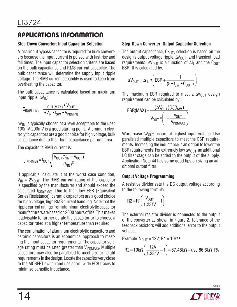
The SHDN pin has a precision voltage threshold with hysteresis which can be used as an undervoltage lockout threshold (UVLO) for the power supply. Undervoltage lockout keeps the LT3724 in shutdown until the supply input voltage is above a certain voltage programmed by the user. The hysteresis voltage prevents noise from falsely tripping UVLO.
Resistors are chosen by first selecting RB. Then:
RA =RB •
VSUPPLY(ON)
1.35V– 1
⎛
⎝⎜⎞
⎠⎟
VSUPPLY(ON) is the input voltage at which the undervoltage lockout is disabled and the supply turns on.
Example: Select RB = 49.9kΩ, VSUPPLY(ON) = 14.5V (based on a 15V minimum input voltage)
RA = 49.9kΩ •
14.5V1.35V
– 1⎛⎝⎜
⎞⎠⎟
= 486.1kΩ (499kΩ resistor is selected)
If low supply current in standby mode is required, select a higher value of RB.
The supply turn off voltage is 9% below turn on. In the example the VSUPPLY(OFF) would be 13.2V.
If additional hysteresis is desired for the enable function, an external positive feedback resistor can be used from the LT3724 regulator output.
The shutdown function can be disabled by connecting the SHDN pin to the VIN through a large value pull-up resistor. This pin contains a low impedance clamp at 6V, so the SHDN pin will sink current from the pull-up resistor(RPU):
ISHDN=
VIN – 6VRPU
Because this arrangement will clamp the SHDN pin to the 6V, it will violate the 5V absolute maximum voltage rating of the pin. This is permitted, however, as long as the absolute maximum input current rating of 1mA is not exceeded. Input SHDN pin currents of <100µA are recommended: a 1MΩ or greater pull-up resistor is typically used for this configuration.
Soft-Start
The soft-start function forces the programmed slew rate while the converter output rises to 95% of regulation, which corresponds to 1.185V on the VFB pin. Once 95% regulation is achieved, the soft-start circuit is disabled. The soft-start circuit will re-enable when the VFB pin drops below 70% of regulation, which corresponds to 300mV of control hysteresis on the VFB pin. This allows for a controlled recovery from a “brown-out” condition.
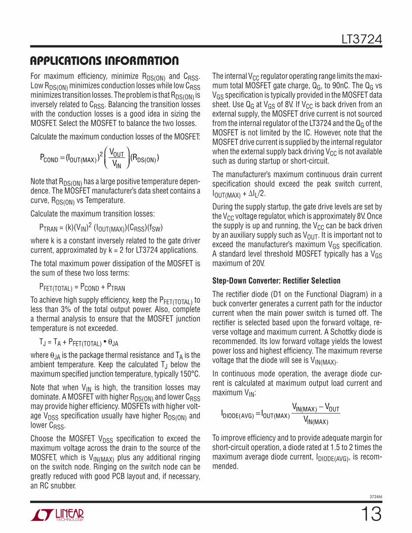
Figure 2. Output Voltage Feedback Divider Figure 3. Undervoltage Lockout Circuit
L1
VFB PIN
R2
R1
VOUT
COUT
3724 F02
SHDN PIN
RA
RB
VSUPPLY
3724 F03
Figure 4.Soft-Start Circuit
RSS
LT3724
VOUT
CSS1
CSS
3724 F04
A
LT3724
163724fd
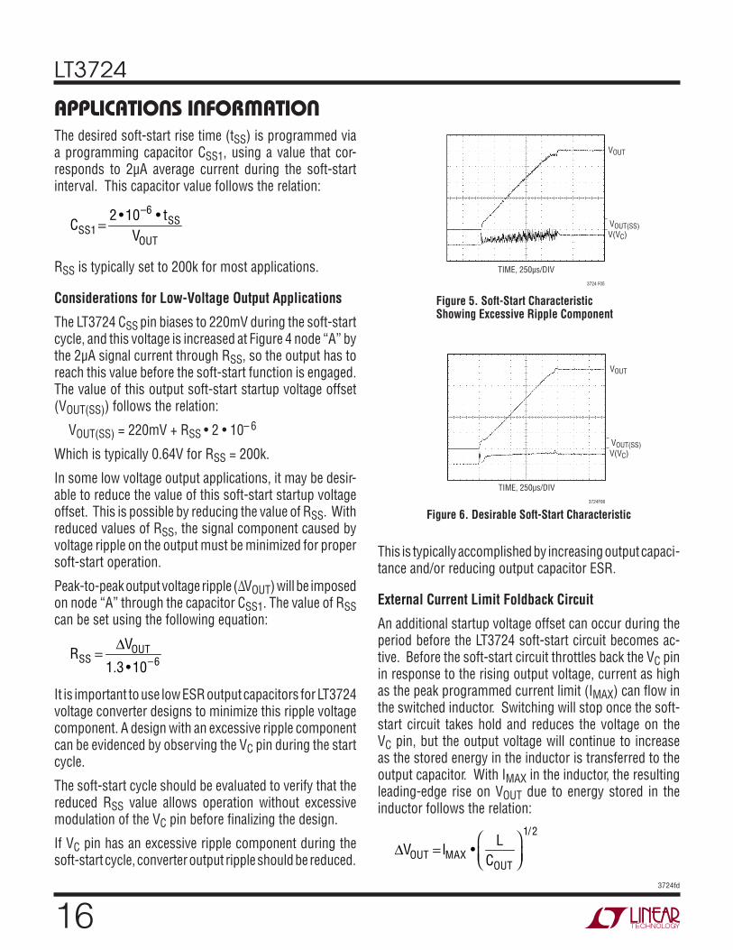
APPLICATIONS INFORMATIONThe desired soft-start rise time (tSS) is programmed via a programming capacitor CSS1, using a value that cor-responds to 2µA average current during the soft-start interval. This capacitor value follows the relation:
CSS1 =
2 •10–6 • tSSVOUT
RSS is typically set to 200k for most applications.
Considerations for Low-Voltage Output Applications
The LT3724 CSS pin biases to 220mV during the soft-start cycle, and this voltage is increased at Figure 4 node “A” by the 2µA signal current through RSS, so the output has to reach this value before the soft-start function is engaged. The value of this output soft-start startup voltage offset (VOUT(SS)) follows the relation:
VOUT(SS) = 220mV + RSS • 2 • 10– 6
Which is typically 0.64V for RSS = 200k.
In some low voltage output applications, it may be desir-able to reduce the value of this soft-start startup voltage offset. This is possible by reducing the value of RSS. With reduced values of RSS, the signal component caused by voltage ripple on the output must be minimized for proper soft-start operation.
Peak-to-peak output voltage ripple (∆VOUT) will be imposed on node “A” through the capacitor CSS1. The value of RSS can be set using the following equation:
RSS =
∆VOUT
1.3 •10–6
It is important to use low ESR output capacitors for LT3724 voltage converter designs to minimize this ripple voltage component. A design with an excessive ripple component can be evidenced by observing the VC pin during the start cycle.
The soft-start cycle should be evaluated to verify that the reduced RSS value allows operation without excessive modulation of the VC pin before finalizing the design.
If VC pin has an excessive ripple component during the soft-start cycle, converter output ripple should be reduced.
This is typically accomplished by increasing output capaci-tance and/or reducing output capacitor ESR.
External Current Limit Foldback Circuit
An additional startup voltage offset can occur during the period before the LT3724 soft-start circuit becomes ac-tive. Before the soft-start circuit throttles back the VC pin in response to the rising output voltage, current as high as the peak programmed current limit (IMAX) can flow in the switched inductor. Switching will stop once the soft-start circuit takes hold and reduces the voltage on the VC pin, but the output voltage will continue to increase as the stored energy in the inductor is transferred to the output capacitor. With IMAX in the inductor, the resulting leading-edge rise on VOUT due to energy stored in the inductor follows the relation:
∆VOUT = IMAX •
LCOUT
1/2
Figure 6. Desirable Soft-Start Characteristic
Figure 5. Soft-Start Characteristic Showing Excessive Ripple Component
TIME, 250µs/DIV
V(VC)VOUT(SS)
VOUT
3724 F05
TIME, 250µs/DIV3724F06
V(VC)VOUT(SS)
VOUT
LT3724
173724fd
APPLICATIONS INFORMATIONInductor current typically does not reach IMAX in the few cycles that occur before soft-start becomes active, but can with high input voltages or small inductors, so the above relation is useful as a worst-case scenario.
This energy transfer increase in output voltage is typically small, but for some low voltage applications with relatively small output capacitors, it can become significant. The volt-age rise can be reduced by increasing output capacitance, which puts additional limitations on COUT for these low voltage supplies. Another approach is to add an external current limit foldback circuit which reduces the value of IMAX during start-up.
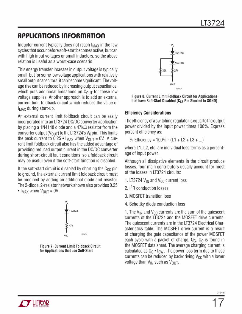
An external current limit foldback circuit can be easily incorporated into an LT3724 DC/DC converter application by placing a 1N4148 diode and a 47kΩ resistor from the converter output (VOUT) to the LT3724’s VC pin. This limits the peak current to 0.25 • IMAX when VOUT = 0V. A cur-rent limit foldback circuit also has the added advantage of providing reduced output current in the DC/DC converter during short-circuit fault conditions, so a foldback circuit may be useful even if the soft-start function is disabled.
If the soft-start circuit is disabled by shorting the CSS pin to ground, the external current limit foldback circuit must be modified by adding an additional diode and resistor. The 2-diode, 2-resistor network shown also provides 0.25 • IMAX when VOUT = 0V.
Efficiency Considerations
The efficiency of a switching regulator is equal to the output power divided by the input power times 100%. Express percent efficiency as:
% Efficiency = 100% - (L1 + L2 + L3 + ...)
where L1, L2, etc. are individual loss terms as a percent-age of input power.
Although all dissipative elements in the circuit produce losses, four main contributors usually account for most of the losses in LT3724 circuits:
1. LT3724 VIN and VCC current loss
2. I2R conduction losses
3. MOSFET transition loss
4. Schottky diode conduction loss
1. The VIN and VCC currents are the sum of the quiescent currents of the LT3724 and the MOSFET drive currents. The quiescent currents are in the LT3724 Electrical Char-acteristics table. The MOSFET drive current is a result of charging the gate capacitance of the power MOSFET each cycle with a packet of charge, QG. QG is found in the MOSFET data sheet. The average charging current is calculated as QG • fSW. The power loss term due to these currents can be reduced by backdriving VCC with a lower voltage than VIN such as VOUT.
Figure 7. Current Limit Foldback Circuit for Applications that use Soft-Start
1N4148
47k
VOUT
VC
3724 F03
Figure 8. Current Limit Foldback Circuit for Applications that have Soft-Start Disabled (CSS Pin Shorted to SGND)
1N4148
27k39k
VOUT
VC
3724 F07
1N4148
LT3724
183724fd
APPLICATIONS INFORMATION2. I2R losses are calculated from the DC resistances of the MOSFET, the inductor, the sense resistor, and the input and output capacitors. In continuous conduction mode the aver-age output current flows through the inductor and RSENSE but is chopped between the MOSFET and the Schottky diode. The resistances of the MOSFET (RDS(ON)) and the RSENSE multiplied by the duty cycle can be summed with the resistances of the inductor and RSENSE to obtain the total series resistance of the circuit. The total conduction power loss is proportional to this resistance and usually accounts for between 2% to 5% loss in efficiency.
3. Transition losses of the MOSFET can be substantial with input voltages greater than 20V. See MOSFET Selection section.
4. The Schottky diode can be a major contributor of power loss especially at high input to output voltage ratios (low duty cycles) where the diode conducts for the majority of the switch period. Lower Vf reduces the losses. Note that oversizing the diode does not always help because as the diode heats up the Vf is reduced and the diode loss term is decreased.
I2R losses and the Schottky diode loss dominate at high load currents. Other losses including CIN and COUT ESR dissipative losses and inductor core losses generally ac-count for less than 2% total additional loss in efficiency.
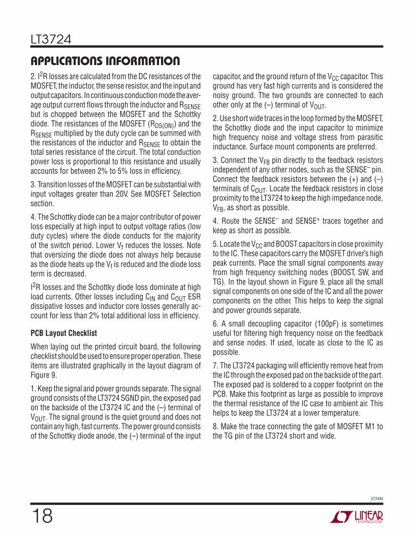
PCB Layout Checklist
When laying out the printed circuit board, the following checklist should be used to ensure proper operation. These items are illustrated graphically in the layout diagram of Figure 9.
1. Keep the signal and power grounds separate. The signal ground consists of the LT3724 SGND pin, the exposed pad on the backside of the LT3724 IC and the (–) terminal of VOUT. The signal ground is the quiet ground and does not contain any high, fast currents. The power ground consists of the Schottky diode anode, the (–) terminal of the input
capacitor, and the ground return of the VCC capacitor. This ground has very fast high currents and is considered the noisy ground. The two grounds are connected to each other only at the (–) terminal of VOUT.
2. Use short wide traces in the loop formed by the MOSFET, the Schottky diode and the input capacitor to minimize high frequency noise and voltage stress from parasitic inductance. Surface mount components are preferred.
3. Connect the VFB pin directly to the feedback resistors independent of any other nodes, such as the SENSE– pin. Connect the feedback resistors between the (+) and (–) terminals of COUT. Locate the feedback resistors in close proximity to the LT3724 to keep the high impedance node, VFB, as short as possible.
4. Route the SENSE– and SENSE+ traces together and keep as short as possible.
5. Locate the VCC and BOOST capacitors in close proximity to the IC. These capacitors carry the MOSFET driver’s high peak currents. Place the small signal components away from high frequency switching nodes (BOOST, SW, and TG). In the layout shown in Figure 9, place all the small signal components on one side of the IC and all the power components on the other. This helps to keep the signal and power grounds separate.
6. A small decoupling capacitor (100pF) is sometimes useful for filtering high frequency noise on the feedback and sense nodes. If used, locate as close to the IC as possible.
7. The LT3724 packaging will efficiently remove heat from the IC through the exposed pad on the backside of the part. The exposed pad is soldered to a copper footprint on the PCB. Make this footprint as large as possible to improve the thermal resistance of the IC case to ambient air. This helps to keep the LT3724 at a lower temperature.
8. Make the trace connecting the gate of MOSFET M1 to the TG pin of the LT3724 short and wide.
LT3724
193724fd
APPLICATIONS INFORMATION
Minimum On-Time Considerations (Step-Down Converters)
Minimum on-time (tTG(ON)) is the least amount of time that the LT3724 is capable of turning the MOSFET on and then off again. It is determined by internal timing delays and the gate charge of the MOSFET. Applications with high input to output differential voltages operate at low duty cycles and may approach this minimum on-time, typically 300nS. The LT3724 switching frequency is internally set to
200kHz, therefore, the minimum duty cycle of the MOSFET switch is 6%. When the duty cycle needs to be less than 6% the output will stay regulated, but cycle skipping may occur. Cycle skipping results in an increase in inductor ripple current. If it is important that cycle skipping does not occur, follow this guideline which takes into account worst case fSW and tTG(ON):
VIN(MAX) ≤ 9 • VOUT
This is only an issue for supplies with VOUT < 7V.
Figure 9. LT3724 Layout Diagram (See PCB Layout Checklist).
4
CBOOST
RSENSE
RA
RCR2
R1
RB
RCSS
VIN–
VIN+
VIN
SHDN
CSS
BURST_EN
VFB
VC
SGND
BOOST
TG
SW
VCC
PGND
SENSE+
SENSE–
+
–
L1M1
D3
3724 F06
LT3724
1
3
5
6
7
8
16
15
14
12
11
10
9
D2
D1
CVCC
CIN
COUT VOUT
CC2
CC1
CSS
17
LT3724
203724fd
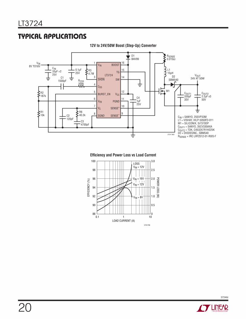
TYPICAL APPLICATIONS12V to 24V/50W Boost (Step-Up) Converter
Efficiency and Power Loss vs Load Current
4
R34.7M
R640.2k
R2187k
R110k
VIN
SHDN
CSS
BURST_EN
VFB
VC
SGND
BOOST
TG
SW
VCC
PGND
SENSE+
SENSE–
M1
D2SBM540
3724 TA02
LT3724
1
3
5
6
7
8
16
15
14
12
11
10
9
C34700pF
C2120pF
C41µF25V
C11500pF
0.1µF25V
COUT1330µF35V
COUT22.2µF x350V
CIN = SANYO, 25SVP33ML1 = VISHAY, IHLP-5050FD-011M1 = SILICONIX, Si7370DPCOUT1 = SANYO, 35CV330AXACOUT2 = TDK, C4532X7R1H225KD2 = DIODESINC., SBM540RSENSE = IRC LRF2512-01-R0I5-F
CIN33µF ×225V
VIN8V TO16V
RSENSE0.015Ω
L110µH
VOUT24V AT 50W
RCSS200k
D1BAV99
LOAD CURRENT (A)0.1
EFFI
CIEN
CY (%
)POW
ER LOSS (W)
100
98
96
94
92
90
88
3.0
2.5
2.0
1.5
1.0
0
0.5
1 10
3724 F08
VIN = 8V
VIN = 12V
VIN = 16V
LOSSVIN = 12V
LT3724
213724fd
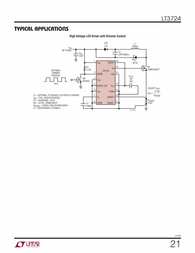
TYPICAL APPLICATIONSHigh Voltage LED Driver with Dimmer Control
4
VIN
SHDN
CSS
BURST_EN
VFB
VC
SGND
BOOST
TG
SW
VCC
PGND
SENSE+
SENSE–
M1ZXMN10A07F
M22N7002
OPTIONALDIMMERCONTROL
1kHz
3724 TA03
LT3724
1
3
5
6
7
8
16
15
14
12
11
10
9
CVCC1µF16V
C1100pF
R14.7M
RSENSE0.5Ω
L1300µH
LED
VIN8V TO 60V
C1 = OPTIONAL TO REDUCE LED RIPPLE CURRENTCIN = TDK, C4532X7R2A225KD1 = DIODESINC., B170M1 = ZETEX, ZXMN10A07FRSENSE = VISHAY, WSL2010R0150FEAL1 = COILTRONICS, CTX300-4
ADJUST ILED:
ILED = 0.15V
RSENSE
C1(OPTIONAL)CIN
22µF
D1B170
LT3724
223724fd
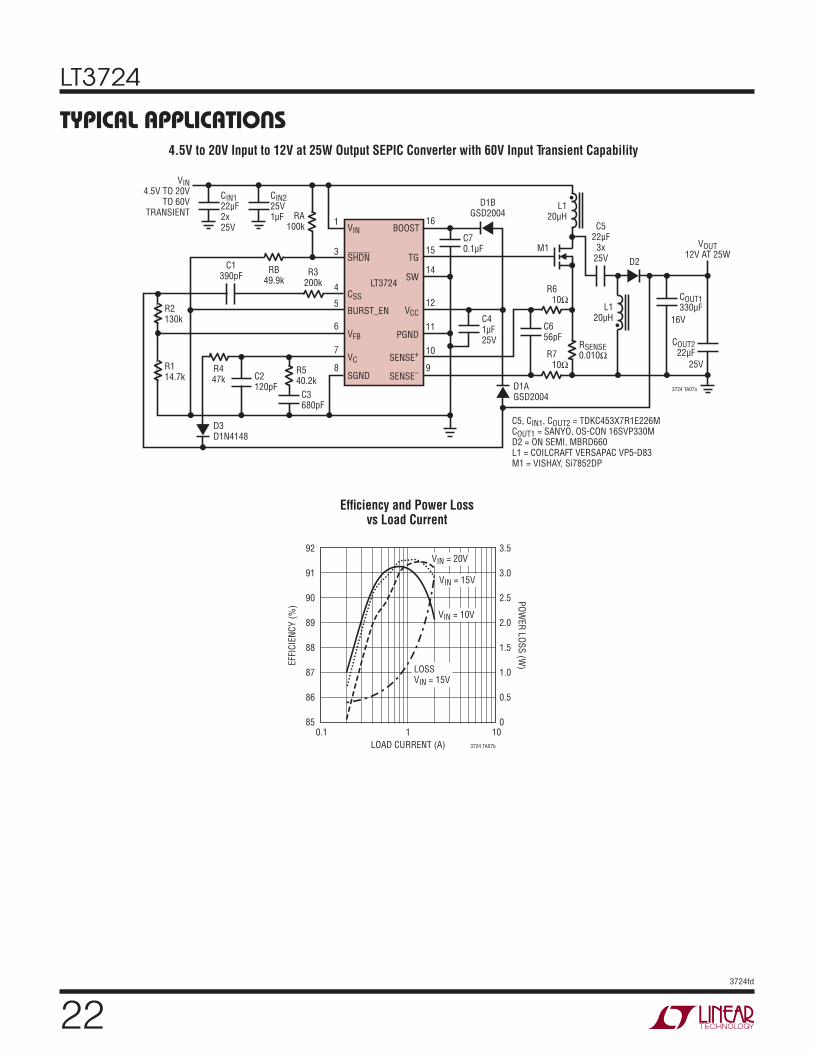
4.5V to 20V Input to 12V at 25W Output SEPIC Converter with 60V Input Transient Capability
Efficiency and Power Loss vs Load Current
4
RB49.9k
RA100k
R540.2k
RSENSE0.010Ω
R2130k
R114.7k
SHDN
CSS
R3200k
BURST_EN
VFB
VC
SGND
TG
SW
VCC
PGND
SENSE+
SENSE–
1
3
5
6
7
8
16
15
14
12
11
10
9
C3680pF
C2120pF
R447k
C70.1µF
C1390pF
CIN225V1µF
CIN122µF2x25V
VIN4.5V TO 20V
TO 60VTRANSIENT
D1AGSD2004
D3D1N4148
L120µH
L120µH
D1BGSD2004
D2
VOUT12V AT 25W
COUT222µF
M1
3724 TA07a
VIN BOOST
LT3724
C41µF25V
COUT1330µF
25V
16VC656pF
R710Ω
R610Ω
C522µF3x
25V
•
•
C5, CIN1, COUT2 = TDKC453X7R1E226MCOUT1 = SANYO, OS-CON 16SVP330MD2 = ON SEMI, MBRD660L1 = COILCRAFT VERSAPAC VP5-D83M1 = VISHAY, Si7852DP
LOAD CURRENT (A)0.1
EFFI
CIEN
CY (%
)POW
ER LOSS (W)
92
91
90
89
88
87
86
85
3.5
3.0
2.5
2.0
1.5
1.0
0
0.5
1 103724 TA07b
VIN = 20V
VIN = 10V
VIN = 15V
LOSSVIN = 15V
TYPICAL APPLICATIONS
LT3724
233724fd
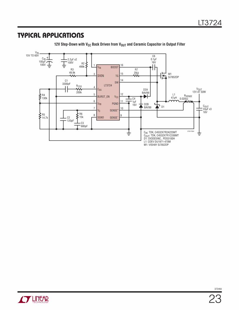
TYPICAL APPLICATIONS12V Step-Down with VCC Back Driven from VOUT and Ceramic Capacitor in Output Filter
4
R349.9k
R720Ω
R2499k
R615k
R4130k
R514.7k
VIN
SHDN
CSS
RCSS
200k
BURST_EN
VFB
VC
SGND
BOOST
TG
SW
VCC
PGND
SENSE+
SENSE–
3724 TA04
LT3724
1
3
5
6
7
8
16
15
14
12
11
10
9
C3680pF
C2120pF
C41µF16V
C60.1µF16V
C13300pF
CIN100µF100V
2.2µF x2100V
VIN15V TO 60V
D2BBAV99
L147µH
D1
D2ABAV99
RSENSE0.020Ω
VOUT12V AT 50W
COUT33µF x316V
CIN: TDK, C4532X7R2A225MTCOUT: TDK, C4532X7R1C336MTD1: DIODESINC., PDS5100HL1: COEV DU1971-470MM1: VISHAY Si7852DP
M1Si7852DP
+
LT3724
243724fd
Information furnished by Linear Technology Corporation is believed to be accurate and reliable. However, no responsibility is assumed for its use. Linear Technology Corporation makes no representa-tion that the interconnection of its circuits as described herein will not infringe on existing patent rights.
FE16 (BC) TSSOP REV I 1210
0.09 – 0.20(.0035 – .0079)
0° – 8°
0.25REF
0.50 – 0.75(.020 – .030)
4.30 – 4.50*(.169 – .177)
1 3 4 5 6 7 8
10
DETAIL B IS THE PART OF THE LEAD FRAME FEATURE
FOR REFERENCE ONLYNO MEASUREMENT PURPOSE
9
4.90 – 5.10*(.193 – .201)
16 1514 13 12 11
1.10(.0433)
MAX
0.05 – 0.15(.002 – .006)
0.65(.0256)
BSC
2.94(.116)
0.48(.019)REF
0.51(.020)REF
0.195 – 0.30(.0077 – .0118)
TYP
2RECOMMENDED SOLDER PAD LAYOUT
0.45 ±0.05
0.65 BSC
4.50 ±0.10
6.60 ±0.10
1.05 ±0.10
2.94(.116)
3.58(.141)
3.58(.141)
MILLIMETERS(INCHES) *DIMENSIONS DO NOT INCLUDE MOLD FLASH. MOLD FLASH
SHALL NOT EXCEED 0.150mm (.006") PER SIDE
NOTE:1. CONTROLLING DIMENSION: MILLIMETERS
2. DIMENSIONS ARE IN
3. DRAWING NOT TO SCALE
SEE NOTE 4
4. RECOMMENDED MINIMUM PCB METAL SIZE FOR EXPOSED PAD ATTACHMENT
6.40(.252)BSC
FE Package16-Lead Plastic TSSOP (4.4mm)
(Reference LTC DWG # 05-08-1663 Rev I)Exposed Pad Variation BC
DETAIL B
PACKAGE DESCRIPTION
LT3724
253724fd
REVISION HISTORYREV DATE DESCRIPTION PAGE NUMBER
D 3/11 Deleted last paragraph of DescriptionMinor text edits made to SW and BOOST pin descriptions in Pin Functions sectionMinor text edits made to Main Control Loop and Current Limit/Short Circuit sections in OperationsRevised High Voltage LED Driver with Dimmer Control in Typical ApplicationsRevised Typical Application drawing and Related Parts list
179
2124
(Revision history begins at Rev D)
LT3724
263724fd
Linear Technology Corporation1630 McCarthy Blvd., Milpitas, CA 95035-7417 (408) 432-1900 FAX: (408) 434-0507 www.linear.com LINEAR TECHNOLOGY CORPORATION 2005
LT 0311 REV D • PRINTED IN USA
RELATED PARTS
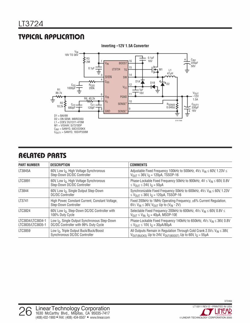
TYPICAL APPLICATIONInverting –12V 1.5A Converter
CC2680pF
CC1120pF
R6, 40.2k
CSS1000pF
RCSS200k
R210.2k
R188.7k
0.1µF
0.1µF16V
1µF16V
R32M
VIN18V TO 36V
VIN
SHDN
CSS
VFB
VC
GND
BOOST
TG
SW
VCC
PGND
SENSE+
SENSE–
+
+
VOUT–12V1.5A
COUT1330µF16V
CIN1220µF50V
L147µH
M1
D2D1BD1A
RSENSE0.040Ω
D1 = BAV99D2 = ON SEMI, MBRD350L1 = COEV, DU1311-470MM1 = VISHAY, Si7370DPCIN1 = SANYO, 50CV220KXCOUT1 = SANYO, 16SVP330M
3724 TA05
LT3724
4
1
3
6
7
8
16
15
14
11
10
9
12
PART NUMBER DESCRIPTION COMMENTS
LT3845A 60V, Low IQ, High Voltage Synchronous Step-Down DC/DC Controller
Adjustable Fixed Frequency 100kHz to 500kHz, 4V≤ VIN ≤ 60V, 1.23V ≤ VOUT ≤ 36V, IQ = 120µA, TSSOP-16
LTC3891 60V, Low IQ, High Voltage Synchronous Step-Down DC/DC Controller
Phase-Lockable Fixed Frequency 50kHz to 900kHz, 4V ≤ VIN ≤ 60V, 0.8V ≤ VOUT ≤ 24V, IQ = 50µA
LT3844 60V, Low IQ, Single Output Step-Down DC/DC Controller
Synchronizable Fixed Frequency 50kHz to 600kHz, 4V≤ VIN ≤ 60V, 1.23V ≤ VOUT ≤ 36V, IQ = 120µA, TSSOP-16
LT3741 High Power, Constant Current, Constant Voltage, Step-Down Controller
Fixed 200kHz to 1MHz Operating Frequency, ±6% Current Regulation, 6V≤ VIN ≤ 36V, VOUT Up to (VIN - 2V)
LTC3824 60V, Low IQ, Step-Down DC/DC Controller with 100% Duty Cycle
Selectable Fixed Frequency 200kHz to 600kHz, 4V≤ VIN ≤ 60V, 0.8V ≤ VOUT ≤ VIN, IQ = 40µA, MSOP-10E
LTC3834/LTC3834-1 LTC3835/LTC3835-1
Low IQ, Single Output Synchronous Step-Down DC/DC Controller with 99% Duty Cycle
Phase-Lockable Fixed Frequency 140kHz to 650kHz, 4V≤ VIN ≤ 36V, 0.8V ≤ VOUT ≤ 10V, IQ = 30µA/80µA
LTC3859 Low IQ, Triple Output Buck/Buck/Boost Synchronous DC/DC Controller
All Outputs Remain in Regulation Through Cold Crank 2.5V≤ VIN ≤ 38V, VOUT(BUCKS) Up to 24V, VOUT(BOOST) Up to 60V, IQ = 55µA


![53619279 Linear Amp Switching Voltage Regulator Handbook[1]](https://img.pdfslide.net/doc/110x75/54f73ea34a7959430c8b4ee1/53619279-linear-amp-switching-voltage-regulator-handbook1.jpg)