Embed Size (px)
Citation preview

This is information on a product in full production.
May 2014 DocID13006 Rev 6 1/37
L5985
2 A step-down switching regulator
Datasheet - production data
Features
2 A DC output current
2.9 V to 18 V input voltage
Output voltage adjustable from 0.6 V
250 kHz switching frequency, programmable up to 1 MHz
Internal soft-start and inhibit
Low dropout operation: 100% duty cycle
Voltage feedforward
Zero load current operation
Overcurrent and thermal protection
VFQFPN8 3 mm x 3 mm package
Applications
Consumer: STB, DVD, DVD recorder, car audio, LCD TV and monitors
Industrial: chargers, PLD, PLA, FPGA
Networking: XDSL, modems, DC-DC modules
Computer: optical storage, hard disk drive, printers, audio/graphic cards
LED driving
Description
The L5985 is a step-down switching regulator with a 2.5 A (min.) current limited embedded Power MOSFET, so it is able to deliver up to 2 A DC current to the load depending on the application condition.
The input voltage can range from 2.9 V to 18 V, while the output voltage can be set starting from 0.6 V to VIN. Having a minimum input voltage of 2.9 V, the device is suitable for a 3.3 V bus.
Requiring a minimum set of external components, the device includes an internal 250 kHz switching frequency oscillator that can be externally adjusted up to 1 MHz.
The VFQFPN8 package with an exposed pad allows reducing the RthJA down to approximately60 °C/W.
VFQFPN8 3 mm x 3 mm
Figure 1. Application circuit
www.st.com

Contents L5985
2/37 DocID13006 Rev 6
Contents
1 Pin settings . . . . . . . . . . . . . . . . . . . . . . . . . . . . . . . . . . . . . . . . . . . . . . . . 4
1.1 Pin connection . . . . . . . . . . . . . . . . . . . . . . . . . . . . . . . . . . . . . . . . . . . . . . 4
1.2 Pin description . . . . . . . . . . . . . . . . . . . . . . . . . . . . . . . . . . . . . . . . . . . . . . 4
2 Maximum ratings . . . . . . . . . . . . . . . . . . . . . . . . . . . . . . . . . . . . . . . . . . . . 5
2.1 Absolute maximum ratings . . . . . . . . . . . . . . . . . . . . . . . . . . . . . . . . . . . . . 5
2.2 Thermal data . . . . . . . . . . . . . . . . . . . . . . . . . . . . . . . . . . . . . . . . . . . . . . . 5
3 Electrical characteristics . . . . . . . . . . . . . . . . . . . . . . . . . . . . . . . . . . . . . 6
4 Functional description . . . . . . . . . . . . . . . . . . . . . . . . . . . . . . . . . . . . . . . 8
4.1 Oscillator and synchronization . . . . . . . . . . . . . . . . . . . . . . . . . . . . . . . . . . 9
4.2 Soft-start . . . . . . . . . . . . . . . . . . . . . . . . . . . . . . . . . . . . . . . . . . . . . . . . . . .11
4.3 Error amplifier and compensation . . . . . . . . . . . . . . . . . . . . . . . . . . . . . . 12
4.4 Overcurrent protection . . . . . . . . . . . . . . . . . . . . . . . . . . . . . . . . . . . . . . . 13
4.5 Inhibit function . . . . . . . . . . . . . . . . . . . . . . . . . . . . . . . . . . . . . . . . . . . . . 14
4.6 Hysteretic thermal shutdown . . . . . . . . . . . . . . . . . . . . . . . . . . . . . . . . . . 14
5 Application information . . . . . . . . . . . . . . . . . . . . . . . . . . . . . . . . . . . . . 15
5.1 Input capacitor selection . . . . . . . . . . . . . . . . . . . . . . . . . . . . . . . . . . . . . . 15
5.2 Inductor selection . . . . . . . . . . . . . . . . . . . . . . . . . . . . . . . . . . . . . . . . . . . 16
5.3 Output capacitor selection . . . . . . . . . . . . . . . . . . . . . . . . . . . . . . . . . . . . 17
5.4 Compensation network . . . . . . . . . . . . . . . . . . . . . . . . . . . . . . . . . . . . . . . 18
5.4.1 Type III compensation network . . . . . . . . . . . . . . . . . . . . . . . . . . . . . . . 19
5.4.2 Type II compensation network . . . . . . . . . . . . . . . . . . . . . . . . . . . . . . . . 23
5.5 Thermal considerations . . . . . . . . . . . . . . . . . . . . . . . . . . . . . . . . . . . . . . 27
5.6 Layout considerations . . . . . . . . . . . . . . . . . . . . . . . . . . . . . . . . . . . . . . . 28
5.7 Application circuit . . . . . . . . . . . . . . . . . . . . . . . . . . . . . . . . . . . . . . . . . . . 30
6 Package information . . . . . . . . . . . . . . . . . . . . . . . . . . . . . . . . . . . . . . . . 34

DocID13006 Rev 6 3/37
L5985 Contents
37
7 Order codes . . . . . . . . . . . . . . . . . . . . . . . . . . . . . . . . . . . . . . . . . . . . . . . 36
8 Revision history . . . . . . . . . . . . . . . . . . . . . . . . . . . . . . . . . . . . . . . . . . . 36

Pin settings L5985
4/37 DocID13006 Rev 6
1 Pin settings
1.1 Pin connection
Figure 2.Pin connection (top view)
1.2 Pin description
OUT
SYNCH
INH
COMP
VCC
GND
FSW
FB
OUT
SYNCH
INH
COMP
VCC
GND
FSW
FB
Table 1. Pin description
N Type Description
1 OUT Regulator output
2 SYNCH
Master/slave synchronization. When it is left floating, a signal with a phase shift of half a period respect to the power turn-on is present at the pin. When connected to an external signal at a frequency higher than the internal one, then the device is synchronized by the external signal, with zero phase shift.
Connecting together the SYNCH pin of two devices, the one with higher frequency works as a master and the other one as a slave; so the two power turn-on have a phase shift of half a period.
3 INHA logical signal (active high) disables the device. With INH higher than 1.9 V the device is OFF and with INH lower than 0.6 V the device is ON.
4 COMP Error amplifier output to be used for loop frequency compensation
5 FBFeedback input. Connecting the output voltage directly to this pin the output voltage is regulated at 0.6 V. To have higher regulated voltages an external resistor divider is required from the Vout to the FB pin.
6 FSW
The switching frequency can be increased connecting an external resistor from the FSW pin and ground. If this pin is left floating, the device works at its free-running frequency of 250 kHz.
7 GND Ground
8 VCC Unregulated DC input voltage

DocID13006 Rev 6 5/37
L5985 Maximum ratings
37
2 Maximum ratings
2.1 Absolute maximum ratings
2.2 Thermal data
Table 2. Absolute maximum ratings
Symbol Parameter Value Unit
Vcc Input voltage 20
V
OUT Output DC voltage -0.3 to VCC
FSW, COMP, SYNCH Analog pin -0.3 to 4
INH Inhibit pin -0.3 to VCC
FB Feedback voltage -0.3 to 1.5
PTOT Power dissipation at TA < 60 °C 1.5 W
TJ Junction temperature range -40 to 150 °C
Tstg Storage temperature range -55 to 150 °C
Table 3. Thermal data
Symbol Parameter Value Unit
RthJA Maximum thermal resistance junction ambient(1) VFQFPN 60 °C/W
1. Package mounted on demonstration board.

Electrical characteristics L5985
6/37 DocID13006 Rev 6
3 Electrical characteristics
TJ = 25 °C, VCC = 12 V, unless otherwise specified.
Table 4. Electrical characteristics
Symbol Parameter Test conditionValues
UnitMin. Typ. Max.
VCC Operating input voltage range (1) 2.9 18
VVCCON turn-on VCC threshold (1) 2.9
VCCHYS VCC UVLO hysteresis (1) 0.175 0.3
RDS(on) MOSFET on resistance140 170
m(1) 140 220
ILIM Maximum limiting current 2.5 2.9 3.3 A
Oscillator
FSW Switching frequency225 250 275
kHz(1) 220 275
VFSW FSW pin voltage 1.254 V
D Duty cycle 0 100 %
FADJ Adjustable switching frequency RFSW = 33 k 1000 kHz
Dynamic characteristics
VFB Feedback voltage 2.9 V < VCC < 18 V(1) 0.593 0.6 0.607 V
DC characteristics
IQ Quiescent current Duty cycle = 0, VFB = 0.8 V 2.4 mA
IQST-BY Total standby quiescent current 20 30 A
Inhibit
INH threshold voltageDevice ON level 0.6
VDevice OFF level 1.9
INH current INH = 0 7.5 10 A
Soft-start
TSS Soft-start durationFSW pin floating 7.4 8.2 9.1
msFSW = 1 MHz, RFSW = 33 k 2

DocID13006 Rev 6 7/37
L5985 Electrical characteristics
37
Error amplifier
VCH High level output voltage VFB < 0.6 V 3V
VCL Low level output voltage VFB > 0.6 V 0.1
IFB Bias source current VFB = 0 V to 0.8 V 1 A
IO SOURCE Source COMP pin VFB = 0.5 V, VCOMP = 1 V 20 mA
IO SINK Sink COMP pin VFB = 0.7 V, VCOMP = 1 V 25 mA
GV Open loop voltage gain (2) 100 dB
Synchronization function
High input voltage 2 3.3V
Low input voltage 1
Slave sink current VSYNCH = 2.9 V 0.7 0.9 mA
Master output amplitude ISOURCE = 4.5 mA 2.0 V
Output pulse width SYNCH floating 110ns
Input pulse width 70
Protection
IFBDISC FB disconnection source current 1 A
TSHDN
Thermal shutdown 150°C
Hysteresis 30
1. Specification referred to TJ from -40 to +125 °C. Specification in the -40 to +125 °C temperature range are assured by design, characterization and statistical correlation.
2. Guaranteed by design.
Table 4. Electrical characteristics (continued)
Symbol Parameter Test conditionValues
UnitMin. Typ. Max.

Functional description L5985
8/37 DocID13006 Rev 6
4 Functional description
The L5985 device is based on a “voltage mode”, constant frequency control. The output voltage VOUT is sensed by the feedback pin (FB) compared to an internal reference (0.6 V) providing an error signal that, compared to a fixed frequency sawtooth, controls the on and off time of the power switch.
The main internal blocks are shown in the block diagram in Figure 3. They are:
A fully integrated oscillator that provides sawtooth to modulate the duty cycle and the synchronization signal. Its switching frequency can be adjusted by an external resistor. The voltage and frequency feedforward are implemented.
The soft-start circuitry to limit inrush current during the startup phase.
The voltage mode error amplifier
The pulse width modulator and the relative logic circuitry necessary to drive the internal power switch.
The high-side driver for embedded P-channel Power MOSFET switch.
The peak current limit sensing block, to handle overload and short-circuit conditions.
A voltage regulator and internal reference. It supplies internal circuitry and provides a fixed internal reference.
A voltage monitor circuitry (UVLO) that checks the input and internal voltages.
The thermal shutdown block, to prevent thermal runaway.
Figure 3. Block diagram

DocID13006 Rev 6 9/37
L5985 Functional description
37
4.1 Oscillator and synchronization
Figure 4 shows the block diagram of the oscillator circuit. The internal oscillator provides a constant frequency clock. Its frequency depends on the resistor externally connected to the FSW pin. In case the FSW pin is left floating, the frequency is 250 kHz; it can be increased as shown in Figure 6 by an external resistor connected to ground.
To improve the line transient performance, keeping the PWM gain constant versus the input voltage, the voltage feedforward is implemented by changing the slope of the sawtooth according to the input voltage change (see Figure 5.a).
The slope of the sawtooth also changes if the oscillator frequency is increased by the external resistor. In this way a frequency feedforward is implemented (Figure 5.b) in order to keep the PWM gain constant versus the switching frequency (see Section 5.4 on page 18 for PWM gain expression).
On the SYNCH pin the synchronization signal is generated. This signal has a phase shift of 180° with respect to the clock. This delay is useful when two devices are synchronized connecting the SYNCH pin together. When SYNCH pins are connected, the device with higher oscillator frequency works as a master, so the slave device switches at the frequency of the master but with a delay of half a period. This minimizes the RMS current flowing through the input capacitor (see the L5988D datasheet).
Figure 4. Oscillator circuit block diagram
The device can be synchronized to work at higher frequency feeding an external clock signal. The synchronization changes the sawtooth amplitude, changing the PWM gain (Figure 5.c). This changing has to be taken into account when the loop stability is studied. To minimize the change of the PWM gain, the free running frequency should be set (with a resistor on the FSW pin) only slightly lower than the external clock frequency. This pre-adjusting of the frequency will change the sawtooth slope in order to get negligible the truncation of sawtooth, due to the external synchronization.
Clock
Generator
Ramp
Generator
FSW
Sawtooth
Clock
Synchronization SYNCHClock
Generator
Ramp
Generator
FSW
Sawtooth
ClockClock
Synchronization SYNCH

Functional description L5985
10/37 DocID13006 Rev 6
Figure 5. Sawtooth: voltage and frequency feedforward; external synchronization
Figure 6. Oscillator frequency versus FSW pin resistor

DocID13006 Rev 6 11/37
L5985 Functional description
37
4.2 Soft-start
The soft-start is essential to assure a correct and safe startup of the step-down converter. It avoids inrush current surge and makes the output voltage increase monotonically.
The soft-start is performed by a staircase ramp on the non-inverting input (VREF) of the error amplifier. So the output voltage slew rate is:
Equation 1
where SRVREF is the slew rate of the non-inverting input, while R1 and R2 the resistor divider to regulate the output voltage (see Figure 7). The soft-start stair case consists of 64 steps of 9.5 mV each one, from 0 V to 0.6 V. The time base of one step is of 32 clock cycles. So the soft-start time and then the output voltage slew rate depend on the switching frequency.
Figure 7. Soft-start scheme
Soft-start time results:
Equation 2
For example with a switching frequency of 250 kHz the SSTIME is 8 ms.
SROUT SRVREF 1R1R2--------+
=
SSTIME32 64Fsw-----------------=

Functional description L5985
12/37 DocID13006 Rev 6
4.3 Error amplifier and compensation
The error amplifier (E/A) provides the error signal to be compared with the sawtooth to perform the pulse width modulation. Its non-inverting input is internally connected to a 0.6 V voltage reference, while its inverting input (FB) and output (COMP) are externally available for feedback and frequency compensation. In this device the error amplifier is a voltage mode operational amplifier, so with high DC gain and low output impedance.
The uncompensated error amplifier characteristics are the following:
In continuous conduction mode (CCM), the transfer function of the power section has two poles due to the LC filter and one zero due to the ESR of the output capacitor. Different kinds of compensation networks can be used depending on the ESR value of the output capacitor. In case the zero introduced by the output capacitor helps to compensate the double pole of the LC filter, a type II compensation network can be used. Otherwise, a type III compensation network has to be used (see Section 5.4 on page 18 for details about the compensation network selection).
Anyway the methodology to compensate the loop is to introduce zeros to obtain a safe phase margin.
Table 5. Uncompensated error amplifier characteristics
Error amplifier Value
Low frequency gain 100 dB
GBWP 4.5 MHz
Slew rate 7 V/s
Output voltage swing 0 to 3.3 V
Maximum source/sink current 25 mA/40 mA

DocID13006 Rev 6 13/37
L5985 Functional description
37
4.4 Overcurrent protection
The L5985 device implements the overcurrent protection sensing current flowing through the Power MOSFET. Due to the noise created by the switching activity of the Power MOSFET, the current sensing is disabled during the initial phase of the conduction time. This avoids an erroneous detection of a fault condition. This interval is generally known as “masking time” or “blanking time”. The masking time is about 200 ns.
When the overcurrent is detected, two different behaviors are possible depending on the operating condition.
1. Output voltage in regulation. When the overcurrent is sensed, the Power MOSFET is switched off and the internal reference (VREF), that biases the non-inverting input of the error amplifier, is set to zero and kept in this condition for a soft-start time (TSS, 2048 clock cycles). After this time, a new soft-start phase takes place and the internal reference begins ramping (see Figure 8.a).
2. Soft-start phase. If the overcurrent limit is reached, the Power MOSFET is turned off implementing the pulse by pulse overcurrent protection. During the soft-start phase, under overcurrent condition, the device can skip pulses in order to keep the output current constant and equal to the current limit. If at the end of the “masking time” the current is higher than the overcurrent threshold, the Power MOSFET is turned off and it will skip one pulse. If, at the next switching on at the end of the “masking time” the current is still higher than the threshold, the device will skip two pulses. This mechanism is repeated and the device can skip up to seven pulses. While, if at the end of the “masking time” the current is lower than the overcurrent threshold, the number of skipped cycles is decreased of one unit. At the end of soft-start phase the output voltage is in regulation and if the overcurrent persists the behavior explained above takes place (see Figure 8.b).
So the overcurrent protection can be summarized as a “hiccup” intervention when the output is in regulation and a constant current during the soft-start phase.
If the output is shorted to ground when the output voltage is on regulation, the overcurrent is triggered and the device starts cycling with a period of 2048 clock cycles between the “hiccup” (Power MOSFET off and no current to the load) and “constant current” with very short on-time and with reduced switching frequency (up to one eighth of normal switching frequency). See Figure 32 on page 33 for short-circuit behavior.

Functional description L5985
14/37 DocID13006 Rev 6
Figure 8. Overcurrent protection strategy
4.5 Inhibit function
The inhibit feature allows to put the device into standby mode. With INH pin higher than 1.9 V the device is disabled and the power consumption is reduced to less than 30 A. With INH pin lower than 0.6 V, the device is enabled. If the INH pin is left floating, an internal pull up ensures that the voltage at the pin reaches the inhibit threshold and the device is disabled. The pin is also VCC compatible.
4.6 Hysteretic thermal shutdown
The thermal shutdown block generates a signal that turns off the power stage if the junction temperature goes above 150 °C. Once the junction temperature goes back to about 130 °C, the device restarts in normal operation. The sensing element is very close to the PDMOS area, so ensuring an accurate and fast temperature detection.

DocID13006 Rev 6 15/37
L5985 Application information
37
5 Application information
5.1 Input capacitor selection
The capacitor connected to the input has to be capable to support the maximum input operating voltage and the maximum RMS input current required by the device. The input capacitor is subject to a pulsed current, the RMS value of which is dissipated over its ESR, affecting the overall system efficiency.
So the input capacitor must have an RMS current rating higher than the maximum RMS input current and an ESR value compliant with the expected efficiency.
The maximum RMS input current flowing through the capacitor can be calculated as:
Equation 3
Where IO is the maximum DC output current, D is the duty cycle, is the efficiency. Considering η = 1, this function has a maximum at D = 0.5 and it is equal to IO/2.
In a specific application the range of possible duty cycles has to be considered in order to find out the maximum RMS input current. The maximum and minimum duty cycles can be calculated as:
Equation 4
and
Equation 5
Where VF is the forward voltage on the freewheeling diode and VSW is voltage drop across the internal PDMOS.In Table 6 some multi-layer ceramic capacitors suitable for this device are reported:
Table 6. Input capacitors
Manufacturer Series Cap value (F) Rated voltage (V)
MURATAGRM31 10 25
GRM55 10 25
TDK C3225 10 25
IRMS IO D2 D
2
---------------–D
2
2-------+=
DMAX
VOUT VF+
VINMIN VSW–-------------------------------------=
DMIN
VOUT VF+
VINMAX VSW–--------------------------------------=

Application information L5985
16/37 DocID13006 Rev 6
5.2 Inductor selection
The inductance value fixes the current ripple flowing through the output capacitor. So the minimum inductance value in order to have the expected current ripple has to be selected. The rule to fix the current ripple value is to have a ripple at 20% - 40% of the output current. In the continuous current mode (CCM), the inductance value can be calculated by the following equation:
Equation 6
Where TON is the conduction time of the internal high-side switch and TOFF is the conduction time of the external diode [in CCM, FSW = 1 / (TON + TOFF)]. The maximum current ripple, at fixed Vout, is obtained at maximum TOFF that is at minimum duty cycle (see Section 5.1 to calculate minimum duty). So fixing IL = 20% to 40% of the maximum output current, the minimum inductance value can be calculated:
Equation 7
where FSW is the switching frequency 1/(TON + TOFF).
For example for VOUT = 3.3 V, VIN = 12 V, IO = 2 A and FSW = 250 kHz the minimum inductance value to have IL = 30% of IO is about 18 H.
The peak current through the inductor is given by:
Equation 8
So if the inductor value decreases, the peak current (that has to be lower than the current limit of the device) increases. The higher is the inductor value, the higher is the average output current that can be delivered, without reaching the current limit.
In Table 7 some inductor part numbers are listed.
Table 7. Inductors
Manufacturer Series Inductor value (H) Saturation current (A)
Wurth PD type S 3.3 to 6.8 2.75 to 4.2
CoilcraftMSS1038 15 to 18 3.2 to 3.6
MSS7341 3.3 to 6.2 2.5 to 3.5
CoiltronicsCD1 15 to 22 2.9 to 3.6
UP2.8B 4.7 to 10 2.7 to 3.9
BI HM76-3 15 to 33 2.5 to 3.7
SUMIDACDRH8D28 4.7 to 10 2.5 to 3.4
CDRH8D28/HP 15 to 22 2.5 to 2.8
ILVIN VOUT–
L------------------------------ TON
VOUT VF+
L---------------------------- TOFF= =
LMIN
VOUT VF+
IMAX----------------------------
1 DMIN–
FSW-----------------------=
IL PK IOIL2--------+=

DocID13006 Rev 6 17/37
L5985 Application information
37
5.3 Output capacitor selection
The current in the capacitor has a triangular waveform which generates a voltage ripple across it. This ripple is due to the capacitive component (charge or discharge of the output capacitor) and the resistive component (due to the voltage drop across its ESR). So the output capacitor has to be selected in order to have a voltage ripple compliant with the application requirements.
The amount of the voltage ripple can be calculated starting from the current ripple obtained by the inductor selection.
Equation 9
Usually the resistive component of the ripple is much higher than the capacitive one, if the output capacitor adopted is not a multi-layer ceramic capacitor (MLCC) with very low ESR value.
The output capacitor is important also for loop stability: it fixes the double LC filter pole and the zero due to its ESR. In Section 5.4, it will be illustrated how to consider its effect in the system stability.
For example with VOUT = 3.3 V, VIN = 12 V, IL = 0.6 A (resulting by the inductor value), in order to have a VOUT = 0.01·VOUT, if the multi-layer capacitors are adopted, 10 F are needed and the ESR effect on the output voltage ripple can be neglected. In case of not negligible ESR (electrolytic or tantalum capacitors), the capacitor is chosen taking into account its ESR value. So in case of 100 µF with ESR = 40 m, the resistive component of the drop dominates and the voltage ripple is 25 mV.
The output capacitor is also important to sustain the output voltage when a load transient with high slew rate is required by the load. When the load transient slew rate exceeds the system bandwidth, the output capacitor provides the current to the load. So if the high slew rate load transient is required by the application, the output capacitor and system bandwidth have to be chosen in order to sustain the load transient.
In Table 8 some capacitor series are listed.
Table 8. Output capacitors
Manufacturer Series Cap value (F) Rated voltage (V) ESR (m)
MURATAGRM32 22 to 100 6.3 to 25 < 5
GRM31 10 to 47 6.3 to 25 < 5
PANASONICECJ 10 to 22 6.3 < 5
EEFCD 10 to 68 6.3 15 to 55
SANYO TPA/B/C 100 to 470 4 to 16 40 to 80
TDK C3225 22 to 100 6.3 < 5
VOUT ESR IMAXIMAX
8 COUT fSW -------------------------------------+=

Application information L5985
18/37 DocID13006 Rev 6
5.4 Compensation network
The compensation network has to assure stability and good dynamic performance. The loop of the L5985 device is based on the voltage mode control. The error amplifier is a voltage operational amplifier with high bandwidth. So selecting the compensation network the E/A will be considered as ideal, that is, its bandwidth is much larger than the system one.
The transfer functions of the PWM modulator and the output LC filter are studied (see Figure 9). The transfer of the function PWM modulator, from the error amplifier output (COMP pin) to the OUT pin, results:
Equation 10
where VS is the sawtooth amplitude. As seen in Section 4.1 on page 9, the voltage feedforward generates a sawtooth amplitude directly proportional to the input voltage, that is:
Equation 11
In this way the PWM modulator gain results constant and equals to:
Equation 12
The synchronization of the device with an external clock provided trough the SYNCH pin can modifies the PWM modulator gain (see Section 4.1 to understand how this gain changes and how to keep it constant in spite of the external synchronization).
The transfer function on the LC filter is given by:
Equation 13
where:
Equation 14
GPW0
VIN
Vs---------=
VS K VIN=
GPW0
VIN
Vs---------
1K---- 9= = =
GLC s 1
s2 fzESR--------------------------+
1s
2 Q f LC----------------------------
s2 fLC------------------- 2
+ +-------------------------------------------------------------------------=
fLC1
2 L COUT 1ESRROUT---------------+
------------------------------------------------------------------------= fzESR1
2 ESR COUT --------------------------------------------=

DocID13006 Rev 6 19/37
L5985 Application information
37
Equation 15
As seen in Section 4.3 on page 12 two different kinds of network can compensate the loop. In the two following paragraphs the guidelines to select the type II and type III compensation network are illustrated.
Figure 9. Error amplifier, PWM modulator and LC output filter
5.4.1 Type III compensation network
The methodology to stabilize the loop consists of placing two zeros to compensate the effect of the LC double pole, so increasing phase margin; then to place one pole in the origin to minimize the dc error on regulated output voltage; finally to place other poles far away the zero dB frequency.
If the equivalent series resistance (ESR) of the output capacitor introduces a zero with a frequency higher than the desired bandwidth (that is: 2 * ESR * COUT < 1 / BW), thetype III compensation network is needed. Multi-layer ceramic capacitors (MLCC) have very low ESR (< 1 m), with very high frequency zero, so type III network is adopted to compensate the loop.
In Figure 10 the type III compensation network is shown. This network introduces two zeros (fZ1, fZ2) and three poles (fP0, fP1, fP2). They are expressed as:
Equation 16
Equation 17
QROUT L COUT ROUT ESR+
L COUT ROUT E SR +------------------------------------------------------------------------------------------ ROUT
VOUT
IOUT--------------=,=
FB COMP
VREF
E/A
PWM
VS
OUT
VCC
COUT
ESR
L
GPW0 GLC
FB COMP
VREF
E/A
PWM
VS
OUT
VCC
COUT
ESR
L
GPW0 GLC
fZ11
2 C3 R1 R3+ ------------------------------------------------= fZ2
12 R4 C4 ------------------------------=
fP0 0= fP11
2 R3 C3 ------------------------------= fP2
1
2 R4
C4 C5C4 C5+--------------------
--------------------------------------------=

Application information L5985
20/37 DocID13006 Rev 6
Figure 10. Type III compensation network
In Figure 11 the Bode diagram of the PWM and LC filter transfer function [GPW0 · GLC(f)] and the open loop gain [GLOOP(f) = GPW0 · GLC(f) · GTYPEIII(f)] are drawn.
Figure 11. Open loop gain: module Bode diagram
The guidelines for positioning the poles and the zeroes and for calculating the component values can be summarized as follow:
1. Choose a value for R1, usually between 1 k and 5 k.
2. Choose a gain (R4/R1) in order to have the required bandwidth (BW), that means:
Equation 18
where K is the feedforward constant and 1 / K is equal to 9.
R4BW K
fLC------------------ R1=
DocID13006 Rev 6 21/37
L5985 Application information
37
3. Calculate C4 by placing the zero at 50% of the output filter double pole frequency (fLC):
Equation 19
4. Calculate C5 by placing the second pole at four times the system bandwidth (BW):
Equation 20
5. Set also the first pole at four times the system bandwidth and also the second zero at the output filter double pole:
Equation 21
The suggested maximum system bandwidth is equal to the switching frequency divided by 3.5 (FSW / 3.5), anyway lower than 100 kHz if the FSW is set higher than 500 kHz.
For example with VOUT = 3.3 V, VIN = 12 V, IO = 2 A, L = 15 H, COUT = 22 F, ESR < 1 m,
the type III compensation network is:
C41
R4 fLC ---------------------------=
C5
C4
2 R4 C4 4 BW 1– --------------------------------------------------------------=
R3
R1
4 BWfLC
----------------- 1–---------------------------= C3
12 R3 4 BW -----------------------------------------=
R1 4.99k= R2 1.1k= R3 150= R4 4.99k= C3 3.3nF= C4 10nF= C5 100pF=
Application information L5985
22/37 DocID13006 Rev 6
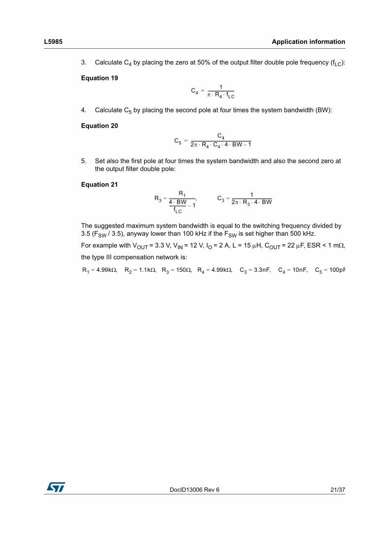
In Figure 12 is shown the module and phase of the open loop gain. The bandwidth is about 75 kHz and the phase margin is 47°.
Figure 12. Open loop gain Bode diagram with ceramic output capacitor

DocID13006 Rev 6 23/37
L5985 Application information
37
5.4.2 Type II compensation network
If the equivalent series resistance (ESR) of the output capacitor introduces a zero with a frequency lower than the desired bandwidth (that is: 2 * ESR * COUT > 1 / BW), this zero helps stabilize the loop. Electrolytic capacitors show not negligible ESR (> 30 m), so with this kind of the output capacitor the type II network combined with the zero of the ESR allows stabilizing the loop.
In Figure 13 the type II network is shown.
Figure 13. Type II compensation network
The singularities of the network are:
Equation 22
fZ11
2 R4 C4 ------------------------------= fP0 0= fP1
1
2 R4
C4 C5C4 C5+--------------------
--------------------------------------------=

Application information L5985
24/37 DocID13006 Rev 6
In Figure 14 the Bode diagram of the PWM and LC filter transfer function [GPW0 · GLC(f)] and the open loop gain [GLOOP(f) = GPW0 · GLC(f) · GTYPEII(f)] are drawn.
Figure 14. Open loop gain: module Bode diagram
The guidelines for positioning the poles and the zeroes and for calculating the component values can be summarized as follow:
1. Choose a value for R1, usually between 1 k and 5 k, in order to have values of C4 and C5 not comparable with parasitic capacitance of the board.
2. Choose a gain (R4/R1) in order to have the required bandwidth (BW), that means:
Equation 23
Where fESR is the ESR zero:
Equation 24
and VS is the saw-tooth amplitude. The voltage feedforward keeps the ratio VS/VIN constant.
3. Calculate C4 by placing the zero one decade below the output filter double pole:
Equation 25
R4
fESR
fLC------------
2 BWfESR------------
VS
VIN--------- R1 =
fESR1
2 ESR COUT --------------------------------------------=
C410
2 R4 fLC -------------------------------=
DocID13006 Rev 6 25/37
L5985 Application information
37
4. Then calculate C3 in order to place the second pole at four times the system bandwidth (BW):
Equation 26
For example with VOUT = 3.3 V, VIN = 12 V, IO = 2 A, L = 15 H, COUT = 330 F,ESR = 50 m the type II compensation network is:
Equation 27
C5
C4
2 R4 C4 4 BW 1– --------------------------------------------------------------=
R1 1.1k= R2 249= R4 10k= C4 68nF= C5 68pF=

Application information L5985
26/37 DocID13006 Rev 6
In Figure 15 is shown the module and phase of the open loop gain. The bandwidth is about 37 kHz and the phase margin is 46°.
Figure 15. Open loop gain Bode diagram with electrolytic/tantalum output capacitor

DocID13006 Rev 6 27/37
L5985 Application information
37
5.5 Thermal considerations
The thermal design is important to prevent the thermal shutdown of the device if junction temperature goes above 150 °C. The three different sources of losses within the device are:
a) Conduction losses due to the not negligible RDS(on) of the power switch; these are equal to:
Equation 28
Where D is the duty cycle of the application and the maximum RDS(on) is 220 m.Note that the duty cycle is theoretically given by the ratio between VOUT an VIN, but actually it is quite higher to compensate the losses of the regulator. So the conduction losses increases compared with the ideal case.
b) Switching losses due to Power MOSFET turn-on and OFF; these can be calculated as:
Equation 29
Where TRISE and TFALL are the overlap times of the voltage across the power switch (VDS) and the current flowing into it during turn ON and turn OFF phases, as shown in Figure 16. TSW is the equivalent switching time. For this device the typical value for the equivalent switching time is 50 ns.
c) Quiescent current losses, calculated as:
Equation 30
where IQ is the quiescent current. (IQ = 2.4 mA).
The junction temperature TJ can be calculated as:
Equation 31
Where TA is the ambient temperature and PTOT is the sum of the power losses just seen.
RthJA is the equivalent thermal resistance junction to ambient of the device; it can be calculated as the parallel of many paths of heat conduction from the junction to the ambient. For this device the path through the exposed pad is the one conducting the largest amount of heat. The RthJA measured on the application demonstration board described in Section 5.7: Application circuit is about 60 °/W.
PON RDSON IOUT 2 D =
PSW VIN IOUT
TRISE TFALL+ 2
------------------------------------------- Fsw VIN IOUT TSW FSW = =
PQ VIN IQ=
TJ TA RthJA PTOT+=

Application information L5985
28/37 DocID13006 Rev 6
Figure 16. Switching losses
5.6 Layout considerations
The PC board layout of the switching DC/DC regulator is very important to minimize the noise injected in high impedance nodes and interferences generated by the high switching current loops.
In a step-down converter the input loop (including the input capacitor, the Power MOSFET and the free wheeling diode) is the most critical one. This is due to the fact that the high value pulsed current are flowing through it. In order to minimize the EMI, this loop has to be as short as possible.
The feedback pin (FB) connection to the external resistor divider is a high impedance node, so the interferences can be minimized placing the routing of the feedback node as far as possible from the high current paths. To reduce the pick-up noise, the resistor divider has to be placed very close to the device. To filter the high frequency noise, a small capacitor (100 nF) can be added as close as possible to the input voltage pin of the device.
Thanks to the exposed pad of the device, the ground plane helps to reduce the thermal resistance junction to ambient; so a large ground plane enhances the thermal performance of the converter allowing high power conversion.

DocID13006 Rev 6 29/37
L5985 Application information
37
In Figure 17 a layout example is shown.
Figure 17. Layout example

Application information L5985
30/37 DocID13006 Rev 6
5.7 Application circuit
In Figure 18 the demonstration board application circuit is shown.
Figure 18. Demonstration board application circuit
Table 9. Component list
Reference Part number Description Manufacturer
C1 GRM31CR61E106KA12 10 µF, 25 V MURATA
C2 GRM31CR61C226KE15B 22 µF, 16 V MURATA
C3 2.2 nF, 50 V
C4 10 nF, 50V
C5 220 pF, 50 V
C6 68 nF, 25 V
R1 4.99 k, 1%, 0.1 W 0603
R2 1.1 k, 1%, 0.1 W 0603
R3 330 , 1%, 0.1 W 0603
R4 2.49 k, 1%, 0.1 W 0603
R5 100 k, 1%, 0.1 W 0603
L1 7447779006 6.8 µH, 30%, 2.91 A Wurth elektronik
D1 STPS2L25V 2 A, 25 V STMicroelectronics
OUT
FB
SYNCHINH
GND
COMP
VCC
L5985
C1
10uFC4 10nF
R1 4.99K
R2 1.1K
D1
STPS2L25U
L1 6.8uH
C3 2.2nFR3 330
C5 220pF
R4 2.49K
FSW
8
3
7
6 45
2
1
C2
22uFC6
68nF
COMP
1Vout=3.3VVIN=3.3V to 18V
R5 1.00K
OUT
FB
SYNCHINH
GND
COMP
VCC
L5985
C1
10uFC4 10nF
R1 4.99K
R2 1.1K
D1
STPS2L25U
L1 6.8uH
C3 2.2nFR3 330
C5 220pF
R4 2.49K
FSW
8
3
7
6 45
2
1
C2
22uFC6
68nF
COMP
1Vout=3.3VVIN=3.3V to 18V
R5 1.00K

DocID13006 Rev 6 31/37
L5985 Application information
37
Figure 19. PCB layout (component side)
Figure 20. PCB layout (bottom side)
Figure 21. PCB layout (front side)
Application information L5985
32/37 DocID13006 Rev 6
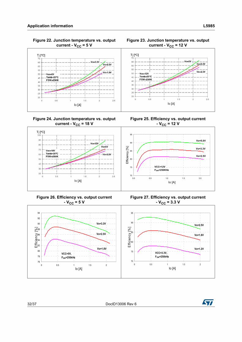
Figure 22. Junction temperature vs. output current - VCC = 5 V
Figure 23. Junction temperature vs. output current - VCC = 12 V
Figure 24. Junction temperature vs. output current - VCC = 18 V
Figure 25. Efficiency vs. output current - VCC = 12 V
Figure 26. Efficiency vs. output current - VCC = 5 V
Figure 27. Efficiency vs. output current - VCC = 3.3 V
70
75
80
85
90
95
0.0 0.5 1.0 1.5 2.0
Io [A]
Eff
icie
ncy
[%]
VCC=12VFSW=250KHz
Vo=5.0V
Vo=3.3V
Vo=2.5V
76
78
80
82
84
86
88
90
92
94
0 0.5 1 1.5 2
Io [A]
Eff
icie
ncy
[%]
VCC=5V,FSW=250kHz
Vo=3.3V
Vo=2.5V
Vo=1.8V
70
75
80
85
90
95
0 0.5 1 1.5 2
Io [A]
Eff
icie
ncy
[%]
VCC=3.3V,FSW=250kHz
Vo=2.5V
Vo=1.8V
Vo=1.2V
DocID13006 Rev 6 33/37
L5985 Application information
37
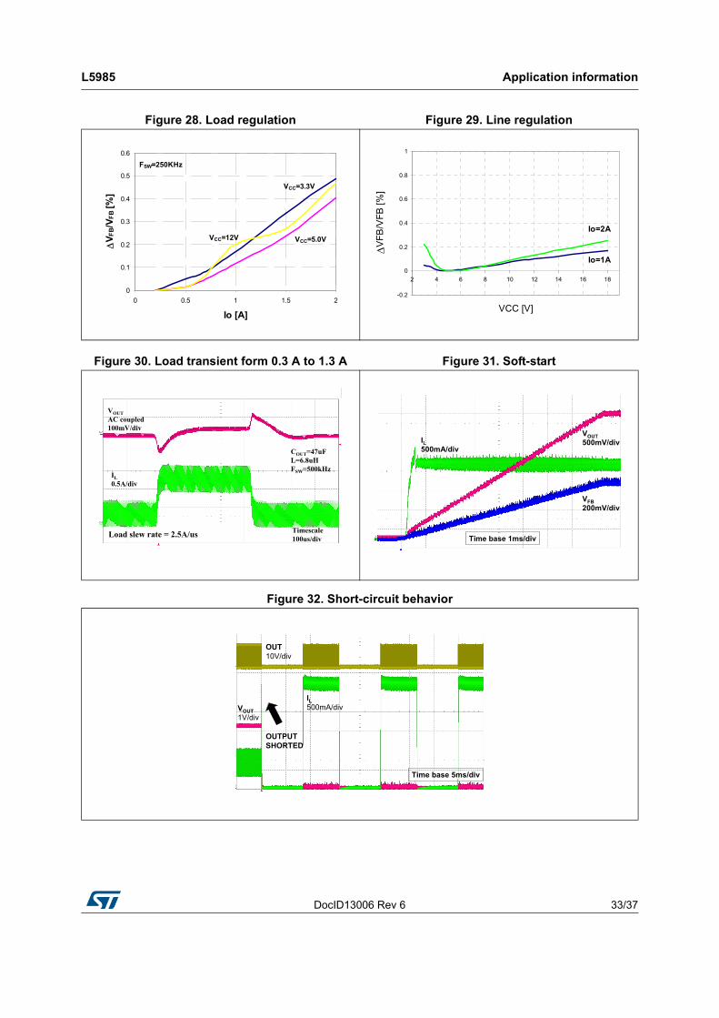
Figure 28. Load regulation Figure 29. Line regulation
0
0.1
0.2
0.3
0.4
0.5
0.6
0 0.5 1 1.5 2
Io [A]
V
FB/V
FB
[%]
VCC=3.3V
VCC=12V VCC=5.0V
FSW=250KHz
-0.2
0
0.2
0.4
0.6
0.8
1
2 4 6 8 10 12 14 16 18
VCC [V]
VF
B/V
FB
[%]
Io=2A
Io=1A
Figure 30. Load transient form 0.3 A to 1.3 A Figure 31. Soft-start
Figure 32. Short-circuit behavior
IL
0.5A/div
VOUT
AC coupled100mV/div
COUT=47uFL=6.8uHFSW=500kHz
Timescale100us/div
IL
0.5A/div
VOUT
AC coupled100mV/div
COUT=47uFL=6.8uHFSW=500kHz
Timescale100us/div
Load slew rate = 2.5A/us
IL
0.5A/div
VOUT
AC coupled100mV/div
COUT=47uFL=6.8uHFSW=500kHz
Timescale100us/div
IL
0.5A/div
VOUT
AC coupled100mV/div
COUT=47uFL=6.8uHFSW=500kHz
Timescale100us/div
Load slew rate = 2.5A/us
VOUT500mV/div
VFB
200mV/div
IL500mA/div
Time base 1ms/div
VOUT500mV/div
VFB
200mV/div
IL500mA/div
Time base 1ms/div
IL500mA/divVOUT
1V/div
OUT10V/div
OUTPUTSHORTED
Time base 5ms/div
IL500mA/divVOUT
1V/div
OUT10V/div
OUTPUTSHORTED
Time base 5ms/div

Package information L5985
34/37 DocID13006 Rev 6
6 Package information
In order to meet environmental requirements, ST offers these devices in different grades of ECOPACK® packages, depending on their level of environmental compliance. ECOPACK specifications, grade definitions and product status are available at: www.st.com. ECOPACK is an ST trademark.
Figure 33. VFQFPN8 (3 x 3 x 1.08 mm) package outline

DocID13006 Rev 6 35/37
L5985 Package information
37
Table 9.VFQFPN8 (3 x 3 x 1.08 mm) package mechanical data
Symbol
Dimensions
mm inch
Min. Typ. Max. Min. Typ. Max.
A 0.80 0.90 1.00 0.0315 0.0354 0.0394
A1 0.02 0.05 0.0008 0.0020
A2 0.70 0.0276
A3 0.20 0.0079
b 0.18 0.23 0.30 0.0071 0.0091 0.0118
D 2.95 3.00 3.05 0.1161 0.1181 0.1200
D2 2.23 2.38 2.48 0.0878 0.0937 0.0976
E 2.95 3.00 3.05 0.1161 0.1181 0.1200
E2 1.65 1.70 1.75 0.0649 0.0669 0.0689
e 0.50 0.0197
L 0.35 0.40 0.45 0.0137 0.0157 0.0177
ddd 0.08 0.0031

Order codes L5985
36/37 DocID13006 Rev 6
7 Order codes
8 Revision history
Table 10. Order codes
Order codes Package Packaging
L5985TRVFQFPN8
3 x 3 x 1.08 mmTape and reel
Table 11. Document revision history
Date Revision Changes
21-Dec-2006 1 Initial release
16-Oct-2007 2 Document status promoted from preliminary data to datasheet
16-Sep-2008 3
Updated: Cover Page, Figure 2 on page 4, Table 1 on page 4, Table 4 on page 6, Figure 8 on page 14 B, Table 7 on page 16, Figure 17 on page 29, Figure 18 on page 30, Table 9 on page 30, Table 9 on page 30
28-Jan-2009 4 Updated: Equation 18
17-Jun-2009 5 Updated Table 4 on page 6 and Figure 6 on page 10
09-May-2014 6
Numbered Equation 22 on page 23.
Added VCC values to titles from Figure 22 on page 32 to Figure 27 on page 32.
Updated Section 6: Package information on page 34 (updated titles,
reversed order of Figure 33 and Table 9, minor modifications).
Updated Table 10: Order codes (removed the L5985 order code
related to the VFQFPN8 in tube, updated “Packaging” of the
L5985TR order code).
Updated cross-references throughout document.
Minor modifications throughout document.

DocID13006 Rev 6 37/37
L5985
37
Please Read Carefully:
Information in this document is provided solely in connection with ST products. STMicroelectronics NV and its subsidiaries (“ST”) reserve theright to make changes, corrections, modifications or improvements, to this document, and the products and services described herein at anytime, without notice.
All ST products are sold pursuant to ST’s terms and conditions of sale.
Purchasers are solely responsible for the choice, selection and use of the ST products and services described herein, and ST assumes noliability whatsoever relating to the choice, selection or use of the ST products and services described herein.
No license, express or implied, by estoppel or otherwise, to any intellectual property rights is granted under this document. If any part of thisdocument refers to any third party products or services it shall not be deemed a license grant by ST for the use of such third party productsor services, or any intellectual property contained therein or considered as a warranty covering the use in any manner whatsoever of suchthird party products or services or any intellectual property contained therein.
UNLESS OTHERWISE SET FORTH IN ST’S TERMS AND CONDITIONS OF SALE ST DISCLAIMS ANY EXPRESS OR IMPLIEDWARRANTY WITH RESPECT TO THE USE AND/OR SALE OF ST PRODUCTS INCLUDING WITHOUT LIMITATION IMPLIEDWARRANTIES OF MERCHANTABILITY, FITNESS FOR A PARTICULAR PURPOSE (AND THEIR EQUIVALENTS UNDER THE LAWSOF ANY JURISDICTION), OR INFRINGEMENT OF ANY PATENT, COPYRIGHT OR OTHER INTELLECTUAL PROPERTY RIGHT.
ST PRODUCTS ARE NOT DESIGNED OR AUTHORIZED FOR USE IN: (A) SAFETY CRITICAL APPLICATIONS SUCH AS LIFESUPPORTING, ACTIVE IMPLANTED DEVICES OR SYSTEMS WITH PRODUCT FUNCTIONAL SAFETY REQUIREMENTS; (B)AERONAUTIC APPLICATIONS; (C) AUTOMOTIVE APPLICATIONS OR ENVIRONMENTS, AND/OR (D) AEROSPACE APPLICATIONSOR ENVIRONMENTS. WHERE ST PRODUCTS ARE NOT DESIGNED FOR SUCH USE, THE PURCHASER SHALL USE PRODUCTS ATPURCHASER’S SOLE RISK, EVEN IF ST HAS BEEN INFORMED IN WRITING OF SUCH USAGE, UNLESS A PRODUCT ISEXPRESSLY DESIGNATED BY ST AS BEING INTENDED FOR “AUTOMOTIVE, AUTOMOTIVE SAFETY OR MEDICAL” INDUSTRYDOMAINS ACCORDING TO ST PRODUCT DESIGN SPECIFICATIONS. PRODUCTS FORMALLY ESCC, QML OR JAN QUALIFIED AREDEEMED SUITABLE FOR USE IN AEROSPACE BY THE CORRESPONDING GOVERNMENTAL AGENCY.
Resale of ST products with provisions different from the statements and/or technical features set forth in this document shall immediately voidany warranty granted by ST for the ST product or service described herein and shall not create or extend in any manner whatsoever, anyliability of ST.
ST and the ST logo are trademarks or registered trademarks of ST in various countries.Information in this document supersedes and replaces all information previously supplied.
The ST logo is a registered trademark of STMicroelectronics. All other names are the property of their respective owners.
© 2014 STMicroelectronics - All rights reserved
STMicroelectronics group of companies
Australia - Belgium - Brazil - Canada - China - Czech Republic - Finland - France - Germany - Hong Kong - India - Israel - Italy - Japan - Malaysia - Malta - Morocco - Philippines - Singapore - Spain - Sweden - Switzerland - United Kingdom - United States of America
www.st.com