Embed Size (px)
Citation preview
LT8610AC/LT8610AC-1
1Rev. B
For more information www.analog.comDocument Feedback
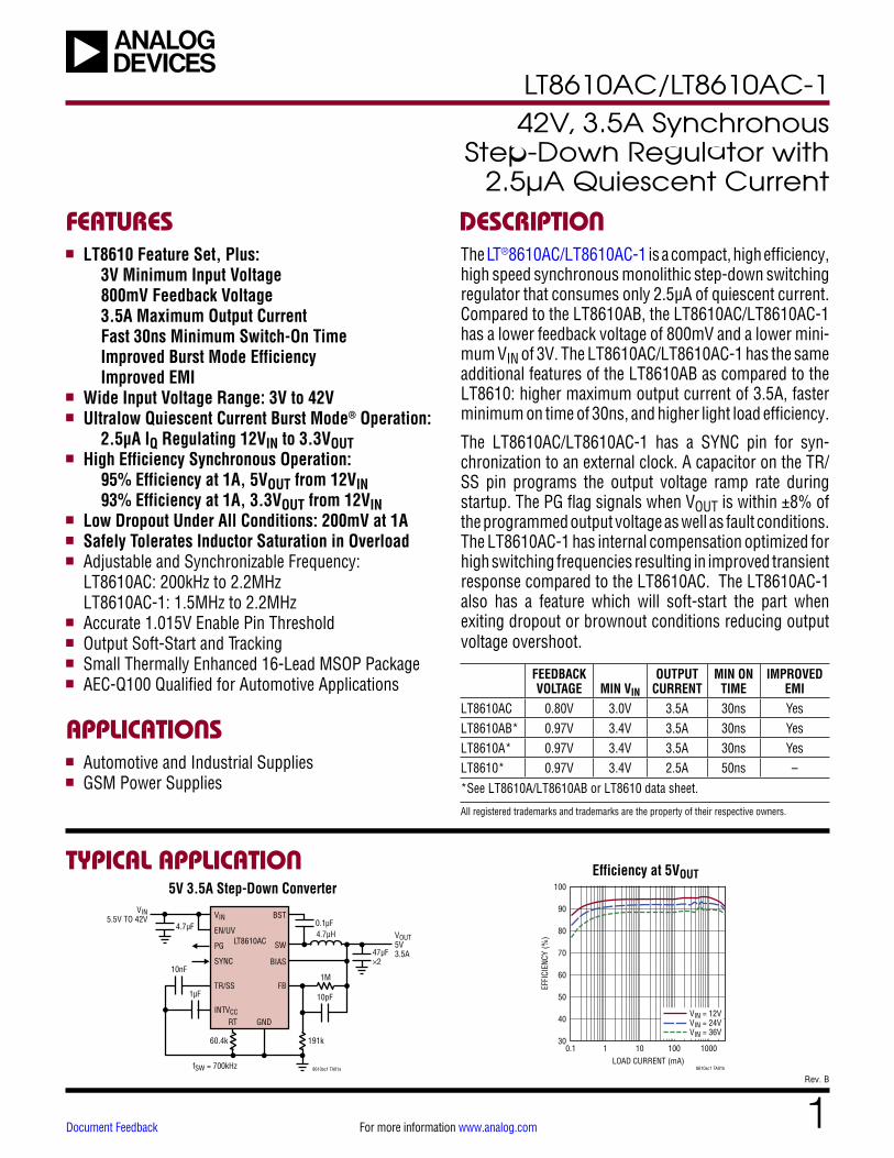
TYPICAL APPLICATION
FEATURES DESCRIPTION
42V, 3.5A Synchronous Step-Down Regulator with
2.5µA Quiescent Current
The LT®8610AC/LT8610AC-1 is a compact, high efficiency, high speed synchronous monolithic step-down switching regulator that consumes only 2.5µA of quiescent current. Compared to the LT8610AB, the LT8610AC/LT8610AC-1 has a lower feedback voltage of 800mV and a lower mini-mum VIN of 3V. The LT8610AC/LT8610AC-1 has the same additional features of the LT8610AB as compared to the LT8610: higher maximum output current of 3.5A, faster minimum on time of 30ns, and higher light load efficiency.
The LT8610AC/LT8610AC-1 has a SYNC pin for syn-chronization to an external clock. A capacitor on the TR/SS pin programs the output voltage ramp rate during startup. The PG flag signals when VOUT is within ±8% of the programmed output voltage as well as fault conditions. The LT8610AC-1 has internal compensation optimized for high switching frequencies resulting in improved transient response compared to the LT8610AC. The LT8610AC-1 also has a feature which will soft-start the part when exiting dropout or brownout conditions reducing output voltage overshoot.
FEEDBACK VOLTAGE MIN VIN
OUTPUT CURRENT
MIN ON TIME
IMPROVED EMI
LT8610AC 0.80V 3.0V 3.5A 30ns YesLT8610AB* 0.97V 3.4V 3.5A 30ns YesLT8610A* 0.97V 3.4V 3.5A 30ns YesLT8610* 0.97V 3.4V 2.5A 50ns –*See LT8610A/LT8610AB or LT8610 data sheet.
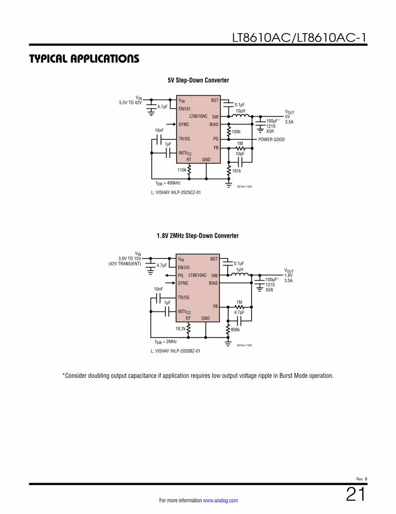
5V 3.5A Step-Down Converter
APPLICATIONS
n LT8610 Feature Set, Plus: 3V Minimum Input Voltage 800mV Feedback Voltage 3.5A Maximum Output Current Fast 30ns Minimum Switch-On Time Improved Burst Mode Efficiency Improved EMI
n Wide Input Voltage Range: 3V to 42Vn Ultralow Quiescent Current Burst Mode® Operation:
2.5μA IQ Regulating 12VIN to 3.3VOUTn High Efficiency Synchronous Operation:
95% Efficiency at 1A, 5VOUT from 12VIN 93% Efficiency at 1A, 3.3VOUT from 12VIN
n Low Dropout Under All Conditions: 200mV at 1An Safely Tolerates Inductor Saturation in Overloadn Adjustable and Synchronizable Frequency:
LT8610AC: 200kHz to 2.2MHz LT8610AC-1: 1.5MHz to 2.2MHzn Accurate 1.015V Enable Pin Thresholdn Output Soft-Start and Trackingn Small Thermally Enhanced 16-Lead MSOP Packagen AEC-Q100 Qualified for Automotive Applications
n Automotive and Industrial Suppliesn GSM Power Supplies
Efficiency at 5VOUT
BSTVIN
EN/UV
PG
SYNC
INTVCC
TR/SS
RT
SWLT8610AC
GND
BIAS
8610ac1 TA01a
FB
0.1µFVOUT5V3.5A
4.7µF
VIN5.5V TO 42V
1µF
10nF
10pF
4.7µH
1M
191k
fSW = 700kHz
60.4k
47µF×2
0.1 1 100010010LOAD CURRENT (mA)
EFFI
CIEN
CY (%
)
80
90
100
8610ac1 TA01b
70
50
60
40
30
VIN = 12VVIN = 24VVIN = 36V
All registered trademarks and trademarks are the property of their respective owners.
LT8610AC/LT8610AC-1
2Rev. B
For more information www.analog.com
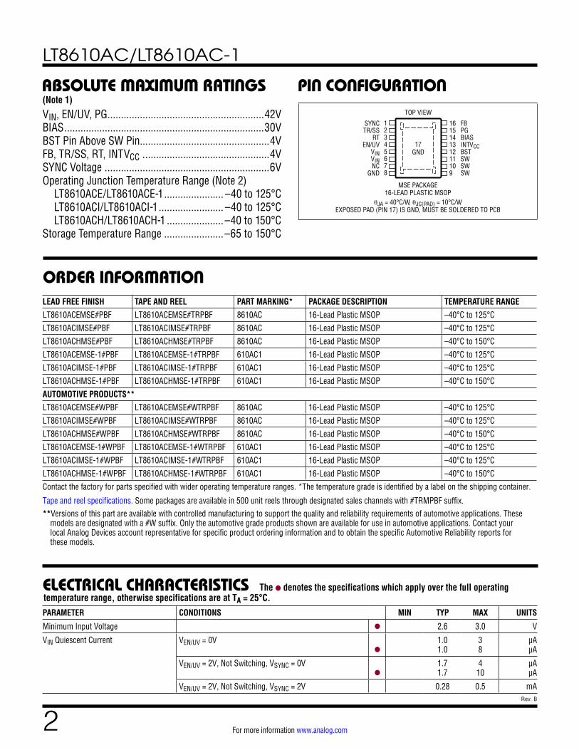
PIN CONFIGURATIONABSOLUTE MAXIMUM RATINGS
VIN, EN/UV, PG ..........................................................42VBIAS ..........................................................................30VBST Pin Above SW Pin................................................4VFB, TR/SS, RT, INTVCC . ..............................................4VSYNC Voltage . ............................................................6VOperating Junction Temperature Range (Note 2) LT8610ACE/LT8610ACE-1 ...................... –40 to 125°C LT8610ACI/LT8610ACI-1 ........................ –40 to 125°C LT8610ACH/LT8610ACH-1 .....................–40 to 150°CStorage Temperature Range ......................–65 to 150°C
(Note 1)
12345678
SYNCTR/SS
RTEN/UV
VINVINNC
GND
161514131211109
FBPGBIASINTVCCBSTSWSWSW
TOP VIEW
17GND
MSE PACKAGE16-LEAD PLASTIC MSOP
θJA = 40°C/W, θJC(PAD) = 10°C/WEXPOSED PAD (PIN 17) IS GND, MUST BE SOLDERED TO PCB
ELECTRICAL CHARACTERISTICS The l denotes the specifications which apply over the full operating temperature range, otherwise specifications are at TA = 25°C.
ORDER INFORMATIONLEAD FREE FINISH TAPE AND REEL PART MARKING* PACKAGE DESCRIPTION TEMPERATURE RANGELT8610ACEMSE#PBF LT8610ACEMSE#TRPBF 8610AC 16-Lead Plastic MSOP –40°C to 125°C
LT8610ACIMSE#PBF LT8610ACIMSE#TRPBF 8610AC 16-Lead Plastic MSOP –40°C to 125°C
LT8610ACHMSE#PBF LT8610ACHMSE#TRPBF 8610AC 16-Lead Plastic MSOP –40°C to 150°C
LT8610ACEMSE-1#PBF LT8610ACEMSE-1#TRPBF 610AC1 16-Lead Plastic MSOP –40°C to 125°C
LT8610ACIMSE-1#PBF LT8610ACIMSE-1#TRPBF 610AC1 16-Lead Plastic MSOP –40°C to 125°C
LT8610ACHMSE-1#PBF LT8610ACHMSE-1#TRPBF 610AC1 16-Lead Plastic MSOP –40°C to 150°C
AUTOMOTIVE PRODUCTS**LT8610ACEMSE#WPBF LT8610ACEMSE#WTRPBF 8610AC 16-Lead Plastic MSOP –40°C to 125°C
LT8610ACIMSE#WPBF LT8610ACIMSE#WTRPBF 8610AC 16-Lead Plastic MSOP –40°C to 125°C
LT8610ACHMSE#WPBF LT8610ACHMSE#WTRPBF 8610AC 16-Lead Plastic MSOP –40°C to 150°C
LT8610ACEMSE-1#WPBF LT8610ACEMSE-1#WTRPBF 610AC1 16-Lead Plastic MSOP –40°C to 125°C
LT8610ACIMSE-1#WPBF LT8610ACIMSE-1#WTRPBF 610AC1 16-Lead Plastic MSOP –40°C to 125°C
LT8610ACHMSE-1#WPBF LT8610ACHMSE-1#WTRPBF 610AC1 16-Lead Plastic MSOP –40°C to 150°C
Contact the factory for parts specified with wider operating temperature ranges. *The temperature grade is identified by a label on the shipping container.
Tape and reel specifications. Some packages are available in 500 unit reels through designated sales channels with #TRMPBF suffix.**Versions of this part are available with controlled manufacturing to support the quality and reliability requirements of automotive applications. These
models are designated with a #W suffix. Only the automotive grade products shown are available for use in automotive applications. Contact your local Analog Devices account representative for specific product ordering information and to obtain the specific Automotive Reliability reports for these models.
PARAMETER CONDITIONS MIN TYP MAX UNITS
Minimum Input Voltage l 2.6 3.0 V
VIN Quiescent Current VEN/UV = 0V
l
1.0 1.0
3 8
µA µA
VEN/UV = 2V, Not Switching, VSYNC = 0V
l
1.7 1.7
4 10
µA µA
VEN/UV = 2V, Not Switching, VSYNC = 2V 0.28 0.5 mA

LT8610AC/LT8610AC-1
3Rev. B
For more information www.analog.com
ELECTRICAL CHARACTERISTICS
Note 1: Stresses beyond those listed under Absolute Maximum Ratings may cause permanent damage to the device. Exposure to any Absolute Maximum Rating condition for extended periods may affect device reliability and lifetime.Note 2: The LT8610ACE/LT8610ACE-1 is guaranteed to meet performance specifications from 0°C to 125°C junction temperature. Specifications over the –40°C to 125°C operating junction temperature range are assured by design, characterization, and correlation with statistical process controls. The LT8610ACI/LT8610ACI-1 is guaranteed over the full –40°C to 125°C
The l denotes the specifications which apply over the full operating temperature range, otherwise specifications are at TA = 25°C.
PARAMETER CONDITIONS MIN TYP MAX UNITS
VIN Current in Regulation VOUT = 0.8V, VIN = 6V, Output Load = 100µA VOUT = 0.8V, VIN = 6V, Output Load = 1mA
l
l
30 225
60 500
µA µA
Feedback Reference Voltage VIN = 6V, ILOAD = 0.5A VIN = 6V, ILOAD = 0.5A
l
0.794 0.788
0.800 0.800
0.806 0.812
V V
Feedback Voltage Line Regulation VIN = 4.0V to 42V, ILOAD = 1A l 0.004 0.02 %/V
Feedback Pin Input Current VFB = 1V –20 20 nA
INTVCC Voltage ILOAD = 0mA, VBIAS = 0V ILOAD = 0mA, VBIAS = 3.3V
3.23 3.25
3.4 3.29
3.57 3.35
V V
INTVCC Undervoltage Lockout 2.37 2.47 2.57 V
BIAS Pin Current Consumption VBIAS = 3.3V, ILOAD = 1A, 2MHz 9.2 mA
Minimum On-Time ILOAD = 1A, SYNC = 0V ILOAD = 1A, SYNC = 3.3V
l
l
15 15
30 30
45 45
ns ns
Minimum Off-Time 95 125 ns
Oscillator Frequency RT = 221k, ILOAD = 1A (LT8610AC Only) RT = 60.4k, ILOAD = 1A (LT8610AC Only) RT = 18.2k, ILOAD = 1A (LT8610AC/LT8610AC-1)
l
l
l
180 665 1.85
210 700 2.00
240 735 2.15
kHz kHz
MHz
Top Power NMOS On-Resistance ISW = 1A 120 mΩ
Top Power NMOS Current Limit l 5 6.7 8 A
Bottom Power NMOS On-Resistance VINTVCC = 3.4V, ISW = 1A 65 mΩ
Bottom Power NMOS Current Limit VINTVCC = 3.4V 3.4 4.3 5.4 A
SW Leakage Current VIN = 42V, VSW = 0V, 42V –1.5 1.5 µA
EN/UV Pin Threshold EN/UV Rising l 0.955 1.015 1.075 V
EN/UV Pin Hysteresis 50 mV
EN/UV Pin Current VEN/UV = 2V –20 20 nA
PG Upper Threshold Offset from VFB VFB Falling l 5 8.0 11 %
PG Lower Threshold Offset from VFB VFB Rising l –11 –8.0 –5 %
PG Hysteresis 0.4 %
PG Leakage VPG = 3.3V –40 40 nA
PG Pull-Down Resistance VPG = 0.1V l 680 2000 Ω
SYNC Threshold SYNC Falling SYNC Rising
0.8 1.6
1.1 2.0
1.4 2.4
V V
TR/SS Source Current l 1.0 2.0 3.2 µA
TR/SS Pull-Down Resistance Fault Condition, TR/SS = 0.1V 230 Ω
operating junction temperature range. The LT8610ACH/LT8610ACH-1 is guaranteed over the full –40°C to 150°C operating junction temperature range. High junction temperatures degrade operating lifetimes. Operating lifetime is derated at junction temperatures greater than 125°C.Note 3: This IC includes overtemperature protection that is intended to protect the device during overload conditions. Junction temperature will exceed 150°C when overtemperature protection is active. Continuous operation above the specified maximum operating junction temperature will reduce lifetime.
LT8610AC/LT8610AC-1
4Rev. B
For more information www.analog.com
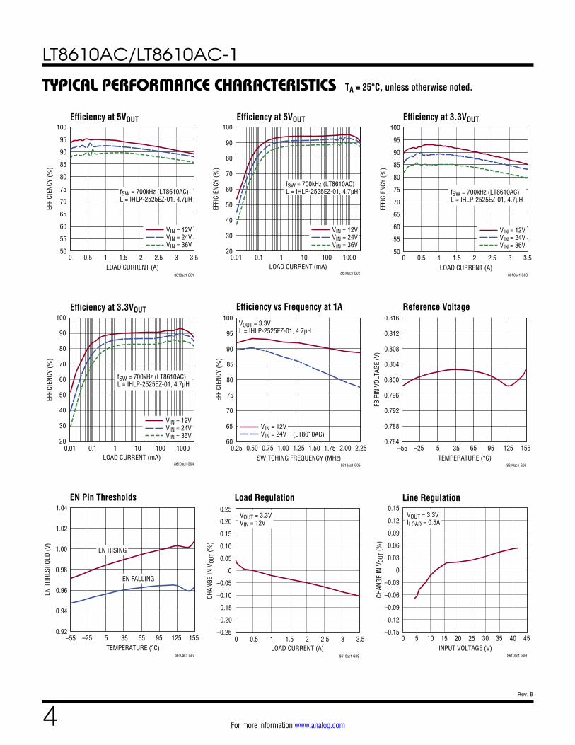
TYPICAL PERFORMANCE CHARACTERISTICS
Efficiency at 3.3VOUT Efficiency vs Frequency at 1A Reference Voltage
Efficiency at 5VOUT Efficiency at 5VOUT Efficiency at 3.3VOUT
LOAD CURRENT (A)0
EFFI
CIEN
CY (%
)
80
90
100
2 3
8610ac1 G01
70
60
75
85
95
65
55
500.5 1 1.5 3.52.5
fSW = 700kHz (LT8610AC)L = IHLP-2525EZ-01, 4.7µH
VIN = 12VVIN = 24VVIN = 36V
LOAD CURRENT (mA)
EFFI
CIEN
CY (%
)
0.01 101 1000100
8610ac1 G02
0.1
80
90
100
70
50
60
40
20
30VIN = 12VVIN = 24VVIN = 36V
fSW = 700kHz (LT8610AC)L = IHLP-2525EZ-01, 4.7µH
0 2 30.5 1 1.5 3.52.5LOAD CURRENT (A)
EFFI
CIEN
CY (%
)
80
90
100
8610ac1 G03
70
60
75
85
95
65
55
50
VIN = 12VVIN = 24VVIN = 36V
fSW = 700kHz (LT8610AC)L = IHLP-2525EZ-01, 4.7µH
0.01 101 10001000.1
VIN = 12VVIN = 24VVIN = 36V
LOAD CURRENT (mA)
30
EFFI
CIEN
CY (%
)
90
100
80
50
70
60
40
8610ac1 G04
20
fSW = 700kHz (LT8610AC)L = IHLP-2525EZ-01, 4.7µH
SWITCHING FREQUENCY (MHz)0.25
80
85
100
1.75
8610ac1 G05
75
70
0.75 1.25 2.251.500.50 1.00 2.00
65
60
90
95
EFFI
CIEN
CY (%
)
VIN = 12VVIN = 24V
VOUT = 3.3VL = IHLP-2525EZ-01, 4.7µH
(LT8610AC)
TEMPERATURE (°C)–55
FB P
IN V
OLTA
GE (V
)
35
8610ac1 G06
0.800
–25 5 65
0.792
0.796
0.788
0.784
0.816
0.812
0.804
0.808
95 125 155
TEMPERATURE (°C)–55
EN T
HRES
HOLD
(V)
35
8610ac1 G07
1.00
–25 5 65
0.96
0.98
0.94
0.92
1.04
1.02
95 125 155
EN RISING
EN FALLING
Line RegulationLoad Regulation
LOAD CURRENT (A)0
–0.25
CHAN
GE IN
VOU
T (%
)
–0.15
–0.05
0.05
0.5 1 1.5 2
8610ac1 G08
2.5
0.15
0.25
–0.20
–0.10
0
0.10
0.20
3.53
VOUT = 3.3VVIN = 12V
INPUT VOLTAGE (V)0
CHAN
GE IN
VOU
T (%
)
0.03
0.09
0.15
40
8610ac1 G09
–0.03
–0.09
0
0.06
0.12
–0.06
–0.12
–0.15105 2015 30 35 4525
VOUT = 3.3VILOAD = 0.5A
TA = 25°C, unless otherwise noted.
EN Pin Thresholds

LT8610AC/LT8610AC-1
5Rev. B
For more information www.analog.com
TYPICAL PERFORMANCE CHARACTERISTICS
No Load Supply Current No Load Supply Current Top FET Current Limit vs Duty Cycle
Top FET Current Limit Bottom FET Current Limit
INPUT VOLTAGE (V)0
0
INPU
T CU
RREN
T (µ
A)
0.5
1.5
2.0
2.5
5.0
3.5
10 20 25 45
8610ac1 G10
1.0
4.0
4.5
3.0
5 15 30 35 40
VOUT = 3.3VIN REGULATION
TEMPERATURE (°C)–55 –25
0
INPU
T CU
RREN
T (µ
A)
10
25
5 65 95
8610ac1 G11
5
20
15
35 125 155
VOUT = 3.3VVIN = 12VIN REGULATION
DUTY CYCLE0
CURR
ENT
LIM
IT (A
)
3.5
4.0
4.5
0.6 1.0
8610ac1 G12
3.00.2 0.4 0.8
5.0
5.5
8.0
7.0
7.5
6.5
6.0
TEMPERATURE (°C)–55
4.50
CURR
ENT
LIM
IT (A
)
4.75
5.00
5.25
5.50
5.75
6.00
6.25
6.50
6.75
7.00
–25 5 35 65
8610ac1 G13
95 125
30% DC
TEMPERATURE (°C)–55
3.00
CURR
ENT
LIM
IT (A
)
3.25
3.50
3.75
4.00
5.50
–25 5 35 65
8610ac1 G14
95 155125
4.25
4.50
4.75
5.00
5.25
Switch Drop
Switch Drop
TEMPERATURE (°C)–55 –25
0
SWIT
CH D
ROP
(mV)
100
250
5 65 95
8610ac1 G15
50
200
150
35 125 155
TOP SW
BOT SW
SWITCH CURRENT = 1A
SWITCH CURRENT (A)0
0
SWIT
CH D
ROP
(mV)
50
150
200
250
2
450
8610ac1 G16
100
10.5 2.51.5 3
300
350
400
TOP SW
BOT SW
Minimum On-Time Minimum Off-Time
TEMPERATURE (°C)–55
25
27
29
31
MIN
IMUM
ON-
TIM
E (n
s)
33
35
37
39
45
5 65 95 125
8610ac1 G17
43
41
–25 35 155
VOUT = 3.3VVOUT = 0.8V
ILOAD = 1.5AVSYNC = 5V
TEMPERATURE (°C)–50
MIN
IMUM
OFF
-TIM
E (n
s)
95
35
8610ac1 G18
80
–25 5 6575
125
120
115
110
105
100
90
85
95 125 155
VOUT = 3.3VILOAD = 0.5A
TA = 25°C, unless otherwise noted.

LT8610AC/LT8610AC-1
6Rev. B
For more information www.analog.com
TYPICAL PERFORMANCE CHARACTERISTICS
Minimum Load to Full Frequency
Burst Frequency
Frequency Foldback
INPUT VOLTAGE (V)
LOAD
CUR
RENT
(mA)
60
70
80
15 25 40
8610ac1 G22
40
20
0
50
30
10
5 10 20 30 35
VOUT = 3.3VfSW = 700kHzPULSE-SKIPPING MODE(LT8610AC)
FB VOLTAGE (V)0
SWIT
CHIN
G FR
EQUE
NCY
(kHz
)
300
400
500
0.6 0.8
8610ac1 G23
200
100
00.2 0.4 0.50.1 0.3 0.7
600
700
800VOUT = 3.3VVIN = 12VVSYNC = 0VRT = 60.4k(LT8610AC)
LOAD CURRENT (mA)0
SWIT
CHIN
G FR
EQUE
NCY
(kHz
)
400
500
600
800
8610ac1 G21
300
200
0200 400 600 700100 300 500
100
800VIN = 12VVOUT = 3.3VL = 4.7µH(LT8610AC)
700
Soft-Start Tracking
Soft-Start Current PG High Thresholds PG Low Thresholds
TR/SS VOLTAGE (V)0
FB V
OLTA
GE (V
)
0.8
1.0
0.6 1.0
8610ac1 G24
0.6
0.4
0.2 0.4 0.8 1.2
0.2
0
TEMPERATURE (°C)–50
SS P
IN C
URRE
NT (µ
A)
2.3
35
8610ac1 G25
2.0
1.8
–25 5 65
1.7
1.6
2.4
2.2
2.1
1.9
95 125 155
VSS = 0.5V
TEMPERATURE (°C)–55
PG T
HRES
HOLD
OFF
SET
FROM
VRE
F (%
)
35
8610ac1 G26
8.0
–25 5 65
7.0
7.5
6.5
6.0
10.0
9.5
8.5
9.0
95 125 155
FB RISING
FB FALLING
TEMPERATURE (°C)–55
PG T
HRES
HOLD
OFF
SET
FROM
VRE
F (%
)
35
8610ac1 G27
–8.0
–25 5 65
–7.0
–7.5
–6.5
–10.0
–6.0
–9.5
–8.5
–9.0
95 125 155
FB RISING
FB FALLING
LOAD CURRENT (A)
DROP
OUT
VOLT
AGE
(mV)
400
8610ac1 G19
200
0
600
800
300
100
500
700
0 0.5 1 1.5 2 2.5 3.53
Dropout Voltage Switching Frequency
TEMPERATURE (°C)–55
SWIT
CHIN
G FR
EQUE
NCY
(kHz
)
730
35
8610ac1 G20
700
680
–25 5 65
670
660
740RT = 60.4k(LT8610AC)
720
710
690
95 125 155
TA = 25°C, unless otherwise noted.
LT8610AC/LT8610AC-1
7Rev. B
For more information www.analog.com
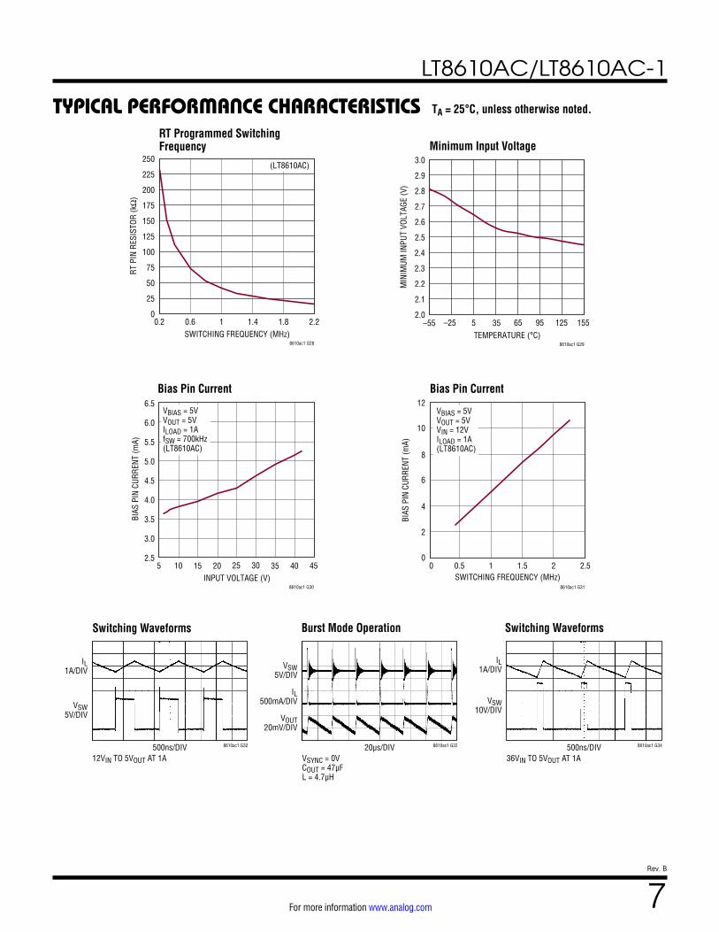
RT Programmed Switching Frequency Minimum Input Voltage
Bias Pin Current Bias Pin Current
SWITCHING FREQUENCY (MHz)0.2
RT P
IN R
ESIS
TOR
(kΩ
)
150
200
250
1.8
8610ac1 G28
100
50
125
175
225
75
25
00.6 1 1.4 2.2
(LT8610AC)
TEMPERATURE (°C)–55
MIN
IMUM
INPU
T VO
LTAG
E (V
)
2.9
35
8610ac1 G29
2.8
2.4
–25 5 65
2.2
2.3
2.1
2.0
3.0
2.7
2.5
2.6
95 125 155
INPUT VOLTAGE (V)5
BIAS
PIN
CUR
RENT
(mA)
4.5
5.5
45
8610ac1 G30
3.5
2.515 25 3510 20 30 40
6.5
4.0
5.0
3.0
6.0VBIAS = 5VVOUT = 5VILOAD = 1AfSW = 700kHz(LT8610AC)
SWITCHING FREQUENCY (MHz)0
0
BIAS
PIN
CUR
RENT
(mA)
2
4
6
8
10
12
0.5 1 1.5 2
8610ac1 G31
2.5
VBIAS = 5VVOUT = 5VVIN = 12VILOAD = 1A(LT8610AC)
TYPICAL PERFORMANCE CHARACTERISTICS
Switching Waveforms Burst Mode Operation Switching Waveforms
IL1A/DIV
VSW5V/DIV
500ns/DIV12VIN TO 5VOUT AT 1A
8610ac1 G32
IL500mA/DIV
VSW5V/DIV
VOUT20mV/DIV
20µs/DIVVSYNC = 0VCOUT = 47µFL = 4.7µH
8610ac1 G33
IL1A/DIV
VSW10V/DIV
500ns/DIV36VIN TO 5VOUT AT 1A
8610ac1 G34
TA = 25°C, unless otherwise noted.
LT8610AC/LT8610AC-1
8Rev. B
For more information www.analog.com
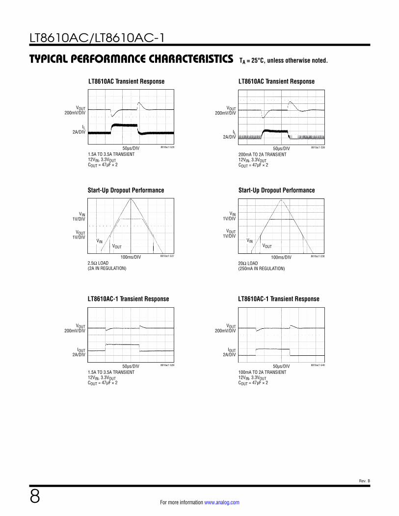
LT8610AC Transient Response
Start-Up Dropout Performance
LT8610AC-1 Transient Response LT8610AC-1 Transient Response
LT8610AC Transient Response
Start-Up Dropout Performance
IL2A/DIV
VOUT200mV/DIV
50µs/DIV1.5A TO 3.5A TRANSIENT12VIN, 3.3VOUTCOUT = 47µF × 2
8610ac1 G35
VOUT1V/DIV
VIN1V/DIV
100ms/DIV2.5Ω LOAD(2A IN REGULATION)
8610ac1 G37
VINVOUT
IL2A/DIV
VOUT200mV/DIV
50µs/DIV200mA TO 2A TRANSIENT12VIN, 3.3VOUTCOUT = 47µF × 2
8610ac1 G36
VOUT1V/DIV
VIN1V/DIV
100ms/DIV20Ω LOAD(250mA IN REGULATION)
8610ac1 G38
VINVOUT
TYPICAL PERFORMANCE CHARACTERISTICS TA = 25°C, unless otherwise noted.
IOUT2A/DIV
VOUT200mV/DIV
50µs/DIV1.5A TO 3.5A TRANSIENT12VIN, 3.3VOUTCOUT = 47µF × 2
8610ac1 G39
IOUT2A/DIV
VOUT200mV/DIV
50µs/DIV100mA TO 2A TRANSIENT12VIN, 3.3VOUTCOUT = 47µF × 2
8610ac1 G40
LT8610AC/LT8610AC-1
9Rev. B
For more information www.analog.com
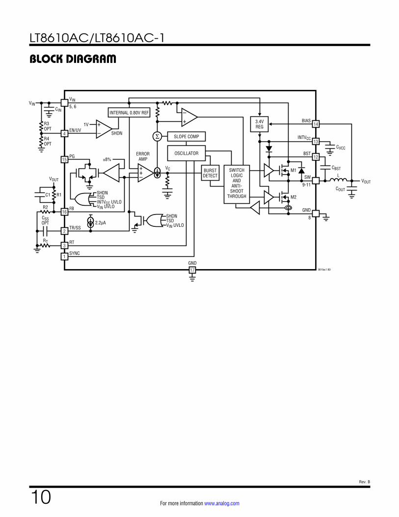
PIN FUNCTIONSSYNC (Pin 1): External Clock Synchronization Input. Ground this pin for low ripple Burst Mode operation at low output loads. Tie to a clock source for synchronization to an external frequency. Apply a DC voltage of 3V or higher or tie to INTVCC for pulse-skipping mode. When in pulse-skipping mode, the IQ will increase to several hundred µA. Do not float this pin.
TR/SS (Pin 2): Output Tracking and Soft-Start Pin. This pin allows user control of output voltage ramp rate during start-up. A TR/SS voltage below 0.8V forces the LT8610AC/LT8610AC-1 to regulate the FB pin to equal the TR/SS pin voltage. When TR/SS is above 0.8V, the tracking function is disabled and the internal reference resumes control of the error amplifier. An internal 2.2μA pull-up current from INTVCC on this pin allows a capacitor to program output voltage slew rate. This pin is pulled to ground with an internal 230Ω MOSFET during shutdown and fault condi-tions; use a series resistor if driving from a low impedance output. This pin may be left floating in the LT8610AC if the tracking function is not needed. A minimum of 100pF of external capacitance must be used on the LT8610AC-1.
RT (Pin 3): A resistor is tied between RT and ground to set the switching frequency.
EN/UV (Pin 4): The LT8610AC/LT8610AC-1 is shut down when this pin is low and active when this pin is high. The hysteretic threshold voltage is 1.015V going up and 0.97V going down. Tie to VIN if the shutdown feature is not used. An external resistor divider from VIN can be used to program a VIN threshold below which the LT8610AC/LT8610AC-1 will shut down.
VIN (Pins 5, 6): The VIN pins supply current to the LT8610AC/LT8610AC-1 internal circuitry and to the internal topside power switch. These pins must be tied together and be locally bypassed. Be sure to place the positive terminal of the input capacitor as close as possible to the VIN pins, and the negative capacitor terminal as close as possible to the GND pins.
NC (Pin 7): No Connect. This pin is not connected to internal circuitry.
SW (Pins 9, 10, 11): The SW pins are the outputs of the internal power switches. Tie these pins together and con-nect them to the inductor and boost capacitor. This node should be kept small on the PCB for good performance.
BST (Pin 12): This pin is used to provide a drive voltage, higher than the input voltage, to the topside power switch. Place a 0.1µF boost capacitor as close as possible to the IC.
INTVCC (Pin 13): Internal 3.4V Regulator Bypass Pin. The internal power drivers and control circuits are pow-ered from this voltage. INTVCC maximum output cur-rent is 20mA. Do not load the INTVCC pin with external circuitry. INTVCC current will be supplied from BIAS if VBIAS > 3.1V, otherwise current will be drawn from VIN. Voltage on INTVCC will vary between 2.8V and 3.4V when VBIAS is between 3.0V and 3.6V. Decouple this pin to power ground with at least a 1μF low ESR ceramic capacitor placed close to the IC.
BIAS (Pin 14): The internal regulator will draw current from BIAS instead of VIN when BIAS is tied to a voltage higher than 3.1V. For output voltages of 3.3V and above this pin should be tied to VOUT. If this pin is tied to a supply other than VOUT use a 1µF local bypass capacitor on this pin.
PG (Pin 15): The PG pin is the open-drain output of an internal comparator. PG remains low until the FB pin is within ±8% of the final regulation voltage, and there are no fault conditions. PG is valid when VIN is above 3.0V, regardless of EN/UV pin state.
FB (Pin 16): The LT8610AC/LT8610AC-1 regulates the FB pin to 0.800V. Connect the feedback resistor divider tap to this pin. Also, connect a phase lead capacitor between FB and VOUT. Typically, this capacitor is 4.7pF to 10pF.
GND (Pin 8, Exposed Pad Pin 17): Ground. These pins are the return path of the internal bottom-side switch and must be tied together. Place the negative terminal of the input capacitor as close to the GND pin and exposed pad as possible. The exposed pad must be soldered to the PCB in order to lower the thermal resistance.
LT8610AC/LT8610AC-1
10Rev. B
For more information www.analog.com
BLOCK DIAGRAM
++–
+–
SLOPE COMP
INTERNAL 0.80V REF
OSCILLATOR
BURSTDETECT
3.4VREG
M1
M2
CBST
COUT
VOUT
8610ac1 BD
SW L
BST
9-11
SWITCHLOGICANDANTI-
SHOOTTHROUGH
ERRORAMP
SHDN
±8%
VC
SHDNTSDINTVCC UVLOVIN UVLO
SHDNTSDVIN UVLO
EN/UV1V +
–4
12
17GND
INTVCC13
BIAS14
GND
8
PG15
FB
R1C1
R3OPT
R4OPT
R2
RT
CSSOPT
VOUT
16
TR/SS2.2µA
2
RT3
SYNC1
VINVIN
CIN
CVCC
5, 6
LT8610AC/LT8610AC-1
11Rev. B
For more information www.analog.com
OPERATIONThe LT8610AC/LT8610AC-1 is a monolithic, constant frequency, current mode step-down DC/DC converter. An oscillator, with frequency set using a resistor on the RT pin, turns on the internal top power switch at the beginning of each clock cycle. Current in the inductor then increases until the top switch current comparator trips and turns off the top power switch. The peak inductor current at which the top switch turns off is controlled by the voltage on the internal VC node. The error amplifier servos the VC node by comparing the voltage on the VFB pin with an internal 0.8V reference. When the load current increases it causes a reduction in the feedback voltage relative to the reference leading the error amplifier to raise the VC voltage until the average inductor current matches the new load current. When the top power switch turns off, the synchronous power switch turns on until the next clock cycle begins or inductor current falls to zero. If overload conditions result in more than 4.3A flowing through the bottom switch, the next clock cycle will be delayed until switch current returns to a safe level.
If the EN/UV pin is low, the LT8610AC/LT8610AC-1 is shut down and draws 1µA from the input. When the EN/UV pin is above 1.015V, the switching regulator will become active.
To optimize efficiency at light loads, the LT8610AC/LT8610AC-1 operates in Burst Mode operation in light load situations. Between bursts, all circuitry associated with controlling the output switch is shut down, reducing the input supply current to 1.7μA. In a typical application, 2.5μA will be consumed from the input supply when regulating with no load. The SYNC pin is tied low to use Burst Mode operation and can be tied to a logic high to use pulse-skipping mode. If a clock is applied to the SYNC pin the part will synchronize to an external clock frequency and operate in pulse-skipping mode. While in pulse-skipping mode the oscillator operates continuously and positive SW transitions are aligned to the clock. During light loads, switch pulses are skipped to regulate the output and the quiescent current will be several hundred µA.
To improve efficiency across all loads, supply current to internal circuitry can be sourced from the BIAS pin when biased at 3.3V or above. Else, the internal circuitry will draw current from VIN. The BIAS pin should be connected to VOUT if the LT8610AC/LT8610AC-1 output is programmed at 3.3V or above.
Comparators monitoring the FB pin voltage will pull the PG pin low if the output voltage varies more than ±8% (typical) from the set point, or if a fault condition is present.
The oscillator reduces the LT8610AC/LT8610AC-1’s oper-ating frequency when the voltage at the FB pin is low. This frequency foldback helps to control the inductor current when the output voltage is lower than the programmed value which occurs during start-up or overcurrent condi-tions. When a clock is applied to the SYNC pin or the SYNC pin is held DC high, the frequency foldback is disabled and the switching frequency will slow down only during overcurrent conditions.
The LT8610AC-1 differs from the LT8610AC in that the internal compensation is optimized for higher switching frequency operation and a TR/SS pin discharge circuit is added to reduce output voltage overshoot when exiting dropout or brownout conditions. The internal compensa-tion change increases the bandwidth of the control loop, which improves transient response. As a consequence the minimum programmable switching frequency of the LT8610AC-1 is increased to 1.5MHz. The SS discharge circuit regulates the TR/SS pin to the same voltage as the FB pin during dropout or brownout. This feature provides some soft-starting when the part exits dropout or brownout which reduces output voltage overshoot. Both of these changes are intended to reduce output voltage overshoot in 2MHz switching frequency applications.

LT8610AC/LT8610AC-1
12Rev. B
For more information www.analog.com
APPLICATIONS INFORMATIONcal converters. By maximizing the time between pulses, the converter quiescent current approaches 2.5µA for a typical application when there is no output load. Therefore, to optimize the quiescent current performance at light loads, the current in the feedback resistor divider must be minimized as it appears to the output as load current.
While in Burst Mode operation the current limit of the top switch is approximately 1.3A for the LT8610AC/LT8610AC-1 resulting in output voltage ripple shown in Figure 2. An increase in output capacitance proportionally decreases the output voltage ripple (Table 1). As load ramps upward from zero the switching frequency will increase but only up to the switching frequency programmed by the resistor at the RT pin as shown in Figure 1a. The output load at which the LT8610AC/LT8610AC-1 reaches the
Figure 1. SW Frequency vs Load Information in Burst Mode Operation (1a) and Pulse-Skipping Mode (1b)
Figure 2. Burst Mode Operation
Minimum Load to Full FrequencyBurst Frequency
(1a) (1b)
LOAD CURRENT (mA)0
SWIT
CHIN
G FR
EQUE
NCY
(kHz
)
400
500
600
800
8610ac1 F01a
300
200
0200 400 600 700100 300 500
100
800VIN = 12VVOUT = 3.3VL = 4.7µH(LT8610AC)
700
INPUT VOLTAGE (V)
LOAD
CUR
RENT
(mA)
60
70
80
15 25 40
8610ac1 F01b
40
20
0
50
30
10
5 10 20 30 35
VOUT = 3.3VfSW = 700kHzPULSE-SKIPPING MODE(LT8610AC)
IL500mA/DIV
VOUT20mV/DIV
VSW5V/DIV
20µs/DIVVSYNC = 0VCOUT = 47µFL = 4.7µH
8610ac1 F02
Achieving Ultralow Quiescent Current
To enhance efficiency at light loads, the LT8610AC/LT8610AC-1 operates in low ripple Burst Mode operation, which keeps the output capacitor charged to the desired output voltage while minimizing the input quiescent cur-rent and minimizing output voltage ripple. In Burst Mode operation the LT8610AC/LT8610AC-1 delivers single pulses of current to the output capacitor followed by sleep periods where the output power is supplied by the output capacitor. While in sleep mode the LT8610AC/LT8610AC-1 consumes 1.7μA.
As the output load decreases, the frequency of single cur-rent pulses decreases (see Figure 1a) and the percentage of time the LT8610AC/LT8610AC-1 is in sleep mode increases, resulting in much higher light load efficiency than for typi-
LT8610AC/LT8610AC-1
13Rev. B
For more information www.analog.com
APPLICATIONS INFORMATIONprogrammed frequency varies based on input voltage, output voltage, and inductor choice.
Inductor value has a very strong effect on Burst Mode ef-ficiency. Larger value inductors allow more charge to be transferred to the output per pulse, which increases both efficiency and output voltage ripple. If higher efficiency is needed in a Burst Mode application, increasing inductor value can be a quick solution.
Table 1. Output Voltage Ripple vs Output Capacitance for LT8610AC when VIN = 12V, VOUT = 3.3V, and L = 4.7µH
OUTPUT CAPACITANCE OUTPUT RIPPLE
47µF 40mV
47µF ×2 20mV
47µF ×4 10mV
For some applications it is desirable for the LT8610AC/LT8610AC-1 to operate in pulse-skipping mode, offering two major differences from Burst Mode operation. First is the clock stays awake at all times and all switching cycles are aligned to the clock. In this mode much of the internal circuitry is awake at all times, increasing quiescent cur-rent to several hundred µA. Second is that full switching frequency is reached at lower output load than in Burst Mode operation (see Figure 1b). To enable pulse-skipping mode, the SYNC pin is tied high either to a logic output or to the INTVCC pin. When a clock is applied to the SYNC pin the LT8610AC/LT8610AC-1 will also operate in pulse-skipping mode.
FB Resistor Network
The output voltage is programmed with a resistor divider between the output and the FB pin. Choose the resistor values according to:
R1=R2 VOUT
0.80V–1⎛
⎝⎜⎞⎠⎟
(1)
Reference designators refer to the Block Diagram. 1% resistors are recommended to maintain output voltage accuracy.
If low input quiescent current and good light-load efficiency are desired, use large resistor values for the FB resistor divider. The current flowing in the divider acts as a load current, and will increase the no-load input current to the converter, which is approximately:
IQ =1.7µA+ VOUT
R1+R2⎛⎝⎜
⎞⎠⎟
VOUTVIN
⎛⎝⎜
⎞⎠⎟
1n
⎛⎝⎜
⎞⎠⎟
(2)
where 1.7µA is the quiescent current of the LT8610AC/LT8610AC-1 and the second term is the current in the feedback divider reflected to the input of the buck operating at its light load efficiency n. For a 3.3V application with R1 = 1M and R2 = 316k, the feedback divider draws 2.5µA. With VIN = 12V and n = 80%, this adds 0.8µA to the 1.7µA quiescent current resulting in 2.5µA no-load current from the 12V supply. Note that this equation implies that the no-load current is a function of VIN; this is plotted in the Typical Performance Characteristics section.
When using large FB resistors, a 4.7pF to 10pF phase-lead capacitor should be connected from VOUT to FB.
Setting the Switching Frequency
The LT8610AC uses a constant frequency PWM architec-ture that can be programmed to switch from 200kHz to 2.2MHz by using a resistor tied from the RT pin to ground. A table showing the necessary RT value for a desired switching frequency is in Table 2A. The LT8610AC-1 can be programmed to switch from 1.5MHz to 2.2MHz. The minimum allowed programmable switching frequency is higher for the LT8610AC-1 compared to the LT8610AC because the LT8610AC-1 has internal compensation which is optimized for higher switching frequencies to improve transient response by increasing control loop bandwidth. A table showing the necessary RT value for a desired switching frequency is shown in Table 2B.
The RT resistor required for a desired switching frequency can be calculated using:
RT =
46.5fSW
– 5.2
(3)
where RT is in kΩ and fSW is the desired switching fre-quency in MHz.
LT8610AC/LT8610AC-1
14Rev. B
For more information www.analog.com
APPLICATIONS INFORMATIONTable 2A. LT8610AC SW Frequency vs RT Value
fSW (MHz) RT (kΩ)
0.2 232
0.3 150
0.4 110
0.5 88.7
0.6 71.5
0.7 60.4
0.8 52.3
1.0 41.2
1.2 33.2
1.4 28.0
1.6 23.7
1.8 20.5
2.0 18.2
2.2 15.8
Table 2B. LT8610AC-1 SW Frequency vs RT Value
fSW (MHz) RT (kΩ)
1.4 28.0
1.6 23.7
1.8 20.5
2.0 18.2
2.2 15.8
Operating Frequency Selection and Trade-Offs
Selection of the operating frequency is a trade-off between efficiency, component size, and input voltage range. The advantage of high frequency operation is that smaller induc-tor and capacitor values may be used. The disadvantages are lower efficiency and a smaller input voltage range.
The highest switching frequency (fSW(MAX)) for a given application can be calculated as follows:
fSW(MAX) =VOUT + VSW(BOT)
tON(MIN) VIN – VSW(TOP) + VSW(BOT)( )
(4)
where VIN is the typical input voltage, VOUT is the output voltage, VSW(TOP) and VSW(BOT) are the internal switch drops (~0.42V, ~0.21V, respectively at maximum load) and tON(MIN) is the minimum top switch on-time (see the Electrical Characteristics). This equation shows that a
slower switching frequency is necessary to accommodate a high VIN/VOUT ratio.
For transient operation, VIN may go as high as the abso-lute maximum rating of 42V regardless of the RT value, however the LT8610AC/LT8610AC-1 will reduce switching frequency as necessary to maintain control of inductor current to assure safe operation.
The LT8610AC/LT8610AC-1 is capable of a maximum duty cycle of greater than 99%, and the VIN-to-VOUT dropout is limited by the RDS(ON) of the top switch. In this mode the LT8610AC/LT8610AC-1 skips switch cycles, resulting in a lower switching frequency than programmed by RT.
For applications that cannot allow deviation from the pro-grammed switching frequency at low VIN/VOUT ratios use the following formula to set switching frequency:
VIN(MIN) =
VOUT + VSW(BOT)
1– fSW • tOFF(MIN)– VSW(BOT) + VSW(TOP)
(5)
where VIN(MIN) is the minimum input voltage without skipped cycles, VOUT is the output voltage, VSW(TOP) and VSW(BOT) are the internal switch drops (~0.42V, ~0.21V, respectively at maximum load), fSW is the switching fre-quency (set by RT), and tOFF(MIN) is the minimum switch off-time. Note that higher switching frequency will increase the minimum input voltage below which cycles will be dropped to achieve higher duty cycle.
Inductor Selection and Maximum Output Current
The LT8610AC/LT8610AC-1 is designed to minimize so-lution size by allowing the inductor to be chosen based on the output load requirements of the application. Dur-ing overload or short-circuit conditions the LT8610AC/LT8610AC-1 safely tolerates operation with a saturated inductor through the use of a high speed peak-current mode architecture.
A good first choice for the inductor value is:
L =
VOUT + VSW(BOT)
fSW (6)
where fSW is the switching frequency in MHz, VOUT is the output voltage, VSW(BOT) is the bottom switch drop (~0.21V) and L is the inductor value in μH.

LT8610AC/LT8610AC-1
15Rev. B
For more information www.analog.com
APPLICATIONS INFORMATIONTo avoid overheating and poor efficiency, an inductor must be chosen with an RMS current rating that is greater than the maximum expected output load of the application. In addition, the saturation current (typically labeled ISAT) rating of the inductor must be higher than the load current plus 1/2 of in inductor ripple current:
IL(PEAK) = ILOAD(MAX)+
12ΔIL
(7)
where ∆IL is the inductor ripple current as calculated in Equation 9 and ILOAD(MAX) is the maximum output load for a given application.
As a quick example, an application requiring 1A output should use an inductor with an RMS rating of greater than 1A and an ISAT of greater than 1.3A. During long duration overload or short-circuit conditions, the inductor RMS rating requirement is greater to avoid overheating of the inductor. To keep the efficiency high, the series resistance (DCR) should be less than 0.04Ω, and the core material should be intended for high frequency applications.
The LT8610AC/LT8610AC-1 limits the peak switch cur-rent in order to protect the switches and the system from overload faults. The top switch current limit (ILIM) is at least 6A at low duty cycles and decreases linearly to 5A at DC = 0.8. The inductor value must then be sufficient to supply the desired maximum output current (IOUT(MAX)), which is a function of the switch current limit (ILIM) and the ripple current.
IOUT(MAX) = ILIM –
ΔIL2
(8)
The peak-to-peak ripple current in the inductor can be calculated as follows:
ΔIL =
VOUTL • fSW
• 1–VOUT
VIN(MAX)
⎛
⎝⎜
⎞
⎠⎟
(9)
where fSW is the switching frequency of the LT8610AC/LT8610AC-1, and L is the value of the inductor. There-fore, the maximum output current that the LT8610AC/LT8610AC-1 will deliver depends on the switch current limit, the inductor value, and the input and output voltages.
The inductor value may have to be increased if the inductor ripple current does not allow sufficient maximum output current (IOUT(MAX)) given the switching frequency, and maximum input voltage used in the desired application.
The optimum inductor for a given application may differ from the one indicated by this design guide. A larger value inductor provides a higher maximum load current and reduces the output voltage ripple. For applications requiring smaller load currents, the value of the inductor may be lower and the LT8610AC/LT8610AC-1 may operate with higher ripple current. This allows use of a physically smaller inductor, or one with a lower DCR resulting in higher efficiency. Be aware that low inductance may result in discontinuous mode operation, which further reduces maximum load current.
Inductor value has a very strong effect on Burst Mode ef-ficiency. Larger value inductors allow more charge to be transferred to the output per pulse, which increases both efficiency and output voltage ripple. If higher efficiency is needed in a Burst Mode application, increasing inductor value can be a quick solution.
For more information about maximum output current and discontinuous operation, see Linear Technology’s Application Note 44.
Finally, for duty cycles greater than 50% (VOUT/VIN > 0.5), a minimum inductance is required to avoid sub-harmonic oscillation. See Application Note 19.
Input Capacitor
Bypass the input of the LT8610AC/LT8610AC-1 circuit with a ceramic capacitor of X7R or X5R type placed as close as possible to the VIN and PGND pins. Y5V types have poor performance over temperature and applied voltage, and should not be used. A 4.7μF to 10μF ceramic capacitor is adequate to bypass the LT8610AC/LT8610AC-1 and will easily handle the ripple current. Note that larger input capacitance is required when a lower switching frequency is used. If the input power source has high impedance, or there is significant inductance due to long wires or cables, additional bulk capacitance may be necessary. This can be provided with a low performance electrolytic capacitor.
LT8610AC/LT8610AC-1
16Rev. B
For more information www.analog.com
APPLICATIONS INFORMATIONStep-down regulators draw current from the input sup-ply in pulses with very fast rise and fall times. The input capacitor is required to reduce the resulting voltage ripple at the LT8610AC/LT8610AC-1 and to force this very high frequency switching current into a tight local loop, mini-mizing EMI. A 4.7μF capacitor is capable of this task, but only if it is placed close to the LT8610AC/LT8610AC-1 (see the PCB Layout section). A second precaution regarding the ceramic input capacitor concerns the maximum input voltage rating of the LT8610AC/LT8610AC-1. A ceramic input capacitor combined with trace or cable inductance forms a high quality (under damped) tank circuit. If the LT8610AC/LT8610AC-1 circuit is plugged into a live sup-ply, the input voltage can ring to twice its nominal value, possibly exceeding the LT8610AC/LT8610AC-1’s voltage rating. This situation is easily avoided (see Linear Technol-ogy Application Note 88).
Output Capacitor and Output Ripple
The output capacitor has two essential functions. Along with the inductor, it filters the square wave generated by the LT8610AC/LT8610AC-1 to produce the DC output. In this role it determines the output ripple, thus low imped-ance at the switching frequency is important. The second function is to store energy in order to satisfy transient loads and stabilize the LT8610AC/LT8610AC-1’s control loop. Ceramic capacitors have very low equivalent series resis-tance (ESR) and provide the best ripple performance. For good starting values, see the Typical Applications section.
Use X5R or X7R types. This choice will provide low output ripple and good transient response. Transient performance can be improved with a higher value output capacitor and the addition of a feedforward capacitor placed between VOUT and FB. Increasing the output capacitance will also decrease the output voltage ripple. A lower value of output capacitor can be used to save space and cost but transient performance will suffer and may cause loop instability. See the Typical Applications in this data sheet for suggested capacitor values.
When choosing a capacitor, special attention should be given to the data sheet to calculate the effective capacitance under the relevant operating conditions of voltage bias and temperature. A physically larger capacitor or one with a higher voltage rating may be required.
Ceramic Capacitors
Ceramic capacitors are small, robust and have very low ESR. However, ceramic capacitors can cause problems when used with the LT8610AC/LT8610AC-1 due to their piezoelectric nature. When in Burst Mode operation, the LT8610AC/LT8610AC-1’s switching frequency depends on the load current, and at very light loads the LT8610AC/LT8610AC-1 can excite the ceramic capacitor at audio fre-quencies, generating audible noise. Since the LT8610AC/LT8610AC-1 operates at a lower current limit during Burst Mode operation, the noise is typically very quiet to a ca-sual ear. If this is unacceptable, use a high performance tantalum or electrolytic capacitor at the output. Low noise ceramic capacitors are also available.
A final precaution regarding ceramic capacitors concerns the maximum input voltage rating of the LT8610AC/LT8610AC-1. As previously mentioned, a ceramic input capacitor combined with trace or cable inductance forms a high quality (underdamped) tank circuit. If the LT8610AC/LT8610AC-1 circuit is plugged into a live supply, the input voltage can ring to twice its nominal value, possibly exceed-ing the LT8610AC/LT8610AC-1’s rating. This situation is easily avoided (see Linear Technology Application Note 88).
Enable Pin
The LT8610AC/LT8610AC-1 is in shutdown when the EN pin is low and active when the pin is high. The rising threshold of the EN comparator is 1.015V, with 45mV of hysteresis. The EN pin can be tied to VIN if the shutdown feature is not used, or tied to a logic level if shutdown control is required.
Adding a resistor divider from VIN to EN programs the LT8610AC/LT8610AC-1 to regulate the output only when VIN is above a desired voltage (see the Block Diagram). Typically, this threshold, VIN(EN), is used in situations where the input supply is current limited, or has a relatively high source resistance. A switching regulator draws constant power from the source, so source current increases as source voltage drops. This looks like a negative resistance load to the source and can cause the source to current limit or latch low under low source voltage conditions. The VIN(EN) threshold prevents the regulator from operating at source voltages where the problems might occur. This

LT8610AC/LT8610AC-1
17Rev. B
For more information www.analog.com
APPLICATIONS INFORMATIONthreshold can be adjusted by setting the values R3 and R4 such that they satisfy the following equation:
VIN(EN) =
R3R4
+1⎛⎝⎜
⎞⎠⎟ •1.015V
(10)
where the LT8610AC/LT8610AC-1 will remain off until VIN is above VIN(EN). Due to the comparator’s hysteresis, switch-ing will not stop until the input falls slightly below VIN(EN).
When operating in Burst Mode operation for light load currents, the current through the VIN(EN) resistor network can easily be greater than the supply current consumed by the LT8610AC/LT8610AC-1. Therefore, the VIN(EN) resistors should be large to minimize their effect on ef-ficiency at low loads.
INTVCC Regulator
An internal low dropout (LDO) regulator produces the 3.4V supply from VIN that powers the drivers and the internal bias circuitry. The INTVCC can supply enough current for the LT8610AC/LT8610AC-1’s circuitry and must be bypassed to ground with a minimum of 1μF ceramic capacitor. Good bypassing is necessary to supply the high transient currents required by the power MOSFET gate drivers. To improve efficiency the internal LDO can also draw cur-rent from the BIAS pin when the BIAS pin is at 3.1V or higher. Typically the BIAS pin can be tied to the output of the LT8610AC/LT8610AC-1, or can be tied to an external supply of 3.3V or above. If BIAS is connected to a supply other than VOUT, be sure to bypass with a local ceramic capacitor. If the BIAS pin is below 3.0V, the internal LDO will consume current from VIN. Applications with high input voltage and high switching frequency where the internal LDO pulls current from VIN will increase die temperature because of the higher power dissipation across the LDO. Do not connect an external load to the INTVCC pin.
Output Voltage Tracking and Soft-Start
The LT8610AC/LT8610AC-1 allows the user to program its output voltage ramp rate by means of the TR/SS pin. An inter-nal 2.2μA pulls up the TR/SS pin to INTVCC. Putting an external capacitor on TR/SS enables soft starting the output to pre-vent current surge on the input supply. During the soft-start ramp the output voltage will proportionally track the TR/SS
pin voltage. For output tracking applications, TR/SS can be externally driven by another voltage source. From 0V to 0.8V, the TR/SS voltage will override the internal 0.8V reference input to the error amplifier, thus regulating the FB pin voltage to that of TR/SS pin. When TR/SS is above 0.8V, tracking is disabled and the feedback voltage will regulate to the internal reference voltage.
The LT8610AC-1 has an additional TR/SS pin feature not included in the LT8610AC. During dropout or brownout, when the FB pin is below the regulated value, the LT8610AC-1 regulates the TR/SS pin to the same voltage as the FB pin. When the dropout or brownout condition goes away, the LT8610AC-1 output voltage will slowly ramp-up with the soft-start voltage preventing output voltage overshoot. Scope shots of the LT8610AC-1 recovering from dropout and short-circuit are shown in Figure 3.
In the LT8610AC, the TR/SS pin may be left floating if the function is not needed. In the LT8610AC-1, the TR/SS pin must have at least 100pF of external capacitance.
VOUT1V/DIV
VSS1V/DIV
VIN5V/DIV
20ms/DIV12VIN → 3.3VIN → 12VIN WITH 3.3VOUT AT 1A
8610ac1 F03a
VOUT1V/DIV
IOUT2A/DIV
VSS1V/DIV
10ms/DIV5.5A BROWNOUT WITH 12VIN, 3.3VOUT AT 1A LOAD
8610ac1 F03b
Figure 3. LT8610AC-1 Soft Starting to Eliminate Output Voltage Overshoot When Exiting Dropout (3a) and Brownout (3b)
(3b)
(3a)
LT8610AC/LT8610AC-1
18Rev. B
For more information www.analog.com
APPLICATIONS INFORMATIONAn active pull-down circuit is connected to the TR/SS pin which will discharge the external soft-start capacitor in the case of fault conditions and restart the ramp when the faults are cleared. Fault conditions that clear the soft-start capacitor are the EN/UV pin transitioning low, VIN voltage falling too low, or thermal shutdown.
Output Power Good
When the LT8610AC/LT8610AC-1’s output voltage is within the ±8% window of the regulation point, which is a VFB voltage in the range of 0.736V to 0.864V (typical), the output voltage is considered good and the open-drain PG pin goes high impedance and is typically pulled high with an external resistor. Otherwise, the internal pull-down device will pull the PG pin low. To prevent glitching both the upper and lower thresholds include 0.4% of hysteresis.
The PG pin is also actively pulled low during several fault conditions: EN/UV pin is below 1.015V, INTVCC has fallen too low, VIN is too low, or thermal shutdown.
Synchronization
To select low ripple Burst Mode operation, tie the SYNC pin below 0.4V (this can be ground or a logic low output). To synchronize the LT8610AC/LT8610AC-1 oscillator to an external frequency connect a square wave (with 20% to 80% duty cycle) to the SYNC pin. The square wave amplitude should have valleys that are below 0.4V and peaks above 2.4V (up to 6V).
The LT8610AC/LT8610AC-1 will not enter Burst Mode operation at low output loads while synchronized to an external clock, but instead will pulse skip to maintain regulation. The LT8610AC may be synchronized over a 200kHz to 2.2MHz range, while the LT8610AC-1 can only be synchronized over a 1.5MHz to 2.2MHz range. The RT resistor should be chosen to set the LT8610AC/LT8610AC-1 switching frequency equal to or below the lowest synchronization input. For example, if the synchro-nization signal will be 500kHz and higher, the RT should be selected for 500kHz. The slope compensation is set by the RT value, while the minimum slope compensation required to avoid subharmonic oscillations is established by the inductor size, input voltage, and output voltage. Since the synchronization frequency will not change the
slopes of the inductor current waveform, if the inductor is large enough to avoid subharmonic oscillations at the frequency set by RT, then the slope compensation will be sufficient for all synchronization frequencies.
For some applications it is desirable for the LT8610AC/LT8610AC-1 to operate in pulse-skipping mode, offering two major differences from Burst Mode operation. First is the clock stays awake at all times and all switching cycles are aligned to the clock. Second is that full switching fre-quency is reached at lower output load than in Burst Mode operation. These two differences come at the expense of increased quiescent current. To enable pulse-skipping mode, the SYNC pin is tied high either to a logic output or to the INTVCC pin.
The LT8610AC/LT8610AC-1 does not operate in forced continuous mode regardless of SYNC signal. Never leave the SYNC pin floating.
Shorted and Reversed Input Protection
The LT8610AC/LT8610AC-1 will tolerate a shorted output. Several features are used for protection during output short-circuit and brownout conditions. The first is the switching frequency will be folded back while the output is lower than the set point to maintain inductor current control. Second, the bottom switch current is monitored such that if inductor current is beyond safe levels switch-ing of the top switch will be delayed until such time as the inductor current falls to safe levels.
The LT8610AC-1 has a feature where the TR/SS pin voltage will be regulated to the same voltage as the FB pin. This means the part will soft-start out of an output short-circuit or brownout condition preventing output voltage overshoot.
Frequency foldback behavior depends on the state of the SYNC pin: If the SYNC pin is low the switching frequency will slow while the output voltage is lower than the pro-grammed level. If the SYNC pin is connected to a clock source or tied high, the LT8610AC/LT8610AC-1 will stay at the programmed frequency without foldback and only slow switching if the inductor current exceeds safe levels.
There is another situation to consider in systems where the output will be held high when the input to the LT8610AC/LT8610AC-1 is absent. This may occur in battery charg-
LT8610AC/LT8610AC-1
19Rev. B
For more information www.analog.com
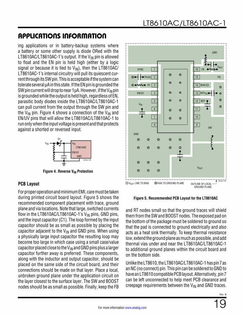
Figure 4. Reverse VIN Protection
VINVIN
D1
LT8610AC
EN/UV
8610ac1 F04
GND
Figure 5. Recommended PCB Layout for the LT8610AC
VOUT
8610ac1 F05
OUTLINE OF LOCALGROUND PLANE
SW
BST
BIAS
INTVCC
GND
9
10
11
12
13
14
15 PG
FB
GND
VOUT16SYNC
TR/SS
RT
EN/UV
VIN
1
2
3
4
5
6
7
8
VOUT LINE TO BIAS VIAS TO GROUND PLANE
ing applications or in battery-backup systems where a battery or some other supply is diode ORed with the LT8610AC/LT8610AC-1’s output. If the VIN pin is allowed to float and the EN pin is held high (either by a logic signal or because it is tied to VIN), then the LT8610AC/ LT8610AC-1’s internal circuitry will pull its quiescent cur-rent through its SW pin. This is acceptable if the system can tolerate several μA in this state. If the EN pin is grounded the SW pin current will drop to near 1µA. However, if the VIN pin is grounded while the output is held high, regardless of EN, parasitic body diodes inside the LT8610AC/LT8610AC-1 can pull current from the output through the SW pin and the VIN pin. Figure 4 shows a connection of the VIN and EN/UV pins that will allow the LT8610AC/LT8610AC-1 to run only when the input voltage is present and that protects against a shorted or reversed input.
APPLICATIONS INFORMATION
PCB Layout
For proper operation and minimum EMI, care must be taken during printed circuit board layout. Figure 5 shows the recommended component placement with trace, ground plane and via locations. Note that large, switched currents flow in the LT8610AC/LT8610AC-1’s VIN pins, GND pins, and the input capacitor (C1). The loop formed by the input capacitor should be as small as possible by placing the capacitor adjacent to the VIN and GND pins. When using a physically large input capacitor the resulting loop may become too large in which case using a small case/value capacitor placed close to the VIN and GND pins plus a larger capacitor further away is preferred. These components, along with the inductor and output capacitor, should be placed on the same side of the circuit board, and their connections should be made on that layer. Place a local, unbroken ground plane under the application circuit on the layer closest to the surface layer. The SW and BOOST nodes should be as small as possible. Finally, keep the FB
and RT nodes small so that the ground traces will shield them from the SW and BOOST nodes. The exposed pad on the bottom of the package must be soldered to ground so that the pad is connected to ground electrically and also acts as a heat sink thermally. To keep thermal resistance low, extend the ground plane as much as possible, and add thermal vias under and near the LT8610AC/LT8610AC-1 to additional ground planes within the circuit board and on the bottom side.
Unlike the LT8610, the LT8610AC/LT8610AC-1 has pin 7 as an NC (no connect) pin. This pin can be soldered to GND to have an LT8610 compatible PCB layout. Alternatively, pin 7 can be left unconnected to help meet PCB clearance and creepage requirements between the VIN and GND traces.

LT8610AC/LT8610AC-1
20Rev. B
For more information www.analog.com
TYPICAL APPLICATIONS
BSTVIN
EN/UV
SYNC
INTVCC
TR/SS
RT
SWLT8610AC-1
GND
BIAS
8610ac1 TA02
PG
FB
0.1µFVOUT5V3.5A
4.7µF
VIN5.5V TO 42V
1µF
10nF
10pF
2.2µH
1M
191k
fSW = 2MHz
L: COILCRAFT XAL 5030
18.2k
47µF*1210X5R
POWER GOOD
100k
5V 2MHz Step-Down Converter 12V Step-Down Converter
BSTVIN
EN/UV
SYNC
INTVCC
TR/SS
RT
SWLT8610AC
GND
BIAS
8610ac1 TA09
PG
FB
0.1µFVOUT12V3.5A
4.7µF
VIN12.5V TO 42V
1µF
10nF
10pF
10µH
1M
71.5k
fSW = 1MHz
41.2k
47µF*1210X5R
POWER GOOD
100k
L: VISHAY IHLP-2525CZ-01
*Consider doubling output capacitance if application requires low output voltage ripple in Burst Mode operation.
Figure 6. LT8610AC Case Temperature Rise
INPUT VOLTAGE (V)CA
SE T
EMPE
RATU
RE R
ISE
(°C)
120
140
16 24 36
8610ac1 F06
80
20
40
0
100
60
8 12 20 28 32
fSW = 2MHzILOAD = 2.5A
fSW = 2MHzILOAD = 3.5A
TA = 25°C
fSW = 1MHzILOAD = 3.5A(LT8610AC)
High Temperature Considerations
For higher ambient temperatures, care should be taken in the layout of the PCB to ensure good heat sinking of the LT8610AC/LT8610AC-1. The exposed pad on the bottom of the package must be soldered to a ground plane. This ground should be tied to large copper layers below with thermal vias; these layers will spread heat dissipated by the LT8610AC/LT8610AC-1. Placing additional vias can reduce thermal resistance further. The maximum load current should be derated as the ambient temperature approaches the maximum junction rating. Power dissipa-tion within the LT8610AC/LT8610AC-1 can be estimated by calculating the total power loss from an efficiency measurement and subtracting the inductor loss. The die temperature is calculated by multiplying the LT8610AC/LT8610AC-1 power dissipation by the thermal resistance from junction to ambient. The LT8610AC/LT8610AC-1 will stop switching and indicate a fault condition if safe junction temperature is exceeded.
Temperature rise of the LT8610AC/LT8610AC-1 is worst when operating at high load, high VIN, and high switching
APPLICATIONS INFORMATIONfrequency. If the case temperature is too high for a given application, then either VIN, switching frequency, or load current can be decreased to reduce the temperature to an acceptable level. Figure 6 shows an example of how case temperature can be managed by reducing VIN, switching frequency, or load.
LT8610AC/LT8610AC-1
21Rev. B
For more information www.analog.com
1.8V 2MHz Step-Down Converter
BSTVIN
EN/UV
SYNC
PG
INTVCC
TR/SS
RT
SWLT8610AC
GND
BIAS
8610ac1 TA06
FB
0.1µFVOUT1.8V3.5A
4.7µF
VIN3.0V TO 15V
(42V TRANSIENT)
1µF
10nF
4.7pF
1µH
1M
806k
fSW = 2MHz
18.2k
100µF*1210X5R
L: VISHAY IHLP-2020BZ-01
5V Step-Down Converter
BSTVIN
EN/UV
SYNC
INTVCC
TR/SS
RT
SWLT8610AC
GND
BIAS
8610ac1 TA03
PG
FB
0.1µFVOUT5V3.5A
4.7µF
VIN5.5V TO 42V
1µF
10nF
10pF
10µH
1M
191k
fSW = 400kHz
110k
100µF*1210X5R
POWER GOOD
100k
L: VISHAY IHLP-2525CZ-01
TYPICAL APPLICATIONS
*Consider doubling output capacitance if application requires low output voltage ripple in Burst Mode operation.

LT8610AC/LT8610AC-1
22Rev. B
For more information www.analog.com
TYPICAL APPLICATIONS
*Consider doubling output capacitance if application requires low output voltage ripple in Burst Mode operation.
3.3V 2MHz Step-Down Converter
BSTVIN
EN/UV
SYNC
PG
INTVCC
TR/SS
RT
SWLT8610AC-1
GND
BIAS
8610ac1 TA04
FB
0.1µFVOUT3.3V3.5A
4.7µF
VIN3.8V TO 27V
(42V TRANSIENT)
1µF
10nF
4.7pF
2.2µH
1M
316k
fSW = 2MHz
18.2k
47µF*1210X5R
L: COILCRAFT XAL 5030
1.8V Step-Down Converter
BSTVIN
EN/UV
SYNC
PG
INTVCC
TR/SS
RT
SWLT8610AC
GND
BIAS
8610ac1 TA07
FB
0.1µFVOUT1.8V3.5A
4.7µF
VIN3.0V TO 42V
1µF
10nF
4.7pF
4.7µH
1M
806k
fSW = 400kHz
110k
47µF*×31210X5R
L: VISHAY IHLP-2020BZ-01
LT8610AC/LT8610AC-1
23Rev. B
For more information www.analog.com
TYPICAL APPLICATIONS
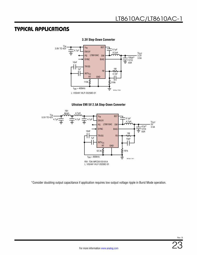
3.3V Step-Down Converter
Ultralow EMI 5V 2.5A Step-Down Converter
BSTVIN
EN/UV
SYNC
PG
INTVCC
TR/SS
RT
SWLT8610AC
GND
BIAS
8610ac1 TA05
FB
0.1µFVOUT3.3V3.5A
4.7µF
VIN3.8V TO 42V
1µF
10nF
4.7pF
8.2µH
1M
316k
fSW = 400kHz
110k
100µF*1210X5R
L: VISHAY IHLP-2525BD-01
BSTVIN
EN/UV
PG
SYNC
INTVCC
TR/SS
RT
SWLT8610AC
GND
BIAS
8610ac1 TA11
FB
0.1µFVOUT5V3.5A
4.7µF
VIN5.5V TO 42V
1µF
10nF
10pF
4.7µH
4.7µH
1M
FB1BEAD
191k
fSW = 800kHz
52.3k
4.7µF4.7µF
47µF*1210X5R
FB1: TDK MPZ2012S101AL: VISHAY IHLP-2020BZ-01
*Consider doubling output capacitance if application requires low output voltage ripple in Burst Mode operation.
LT8610AC/LT8610AC-1
24Rev. B
For more information www.analog.com
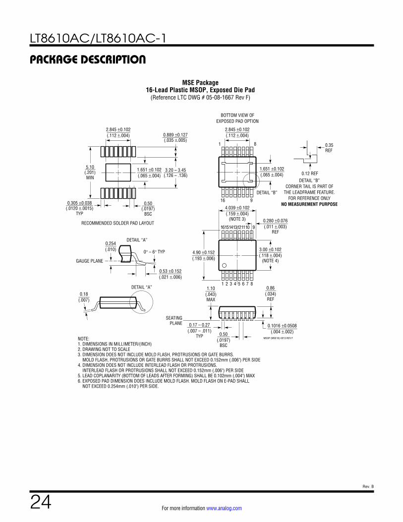
PACKAGE DESCRIPTION
MSOP (MSE16) 0213 REV F
0.53 ±0.152(.021 ±.006)
SEATINGPLANE
0.18(.007)
1.10(.043)MAX
0.17 – 0.27(.007 – .011)
TYP
0.86(.034)REF
0.50(.0197)
BSC
16
16151413121110
1 2 3 4 5 6 7 8
9
9
1 8
NOTE:1. DIMENSIONS IN MILLIMETER/(INCH)2. DRAWING NOT TO SCALE3. DIMENSION DOES NOT INCLUDE MOLD FLASH, PROTRUSIONS OR GATE BURRS. MOLD FLASH, PROTRUSIONS OR GATE BURRS SHALL NOT EXCEED 0.152mm (.006") PER SIDE4. DIMENSION DOES NOT INCLUDE INTERLEAD FLASH OR PROTRUSIONS. INTERLEAD FLASH OR PROTRUSIONS SHALL NOT EXCEED 0.152mm (.006") PER SIDE5. LEAD COPLANARITY (BOTTOM OF LEADS AFTER FORMING) SHALL BE 0.102mm (.004") MAX6. EXPOSED PAD DIMENSION DOES INCLUDE MOLD FLASH. MOLD FLASH ON E-PAD SHALL NOT EXCEED 0.254mm (.010") PER SIDE.
0.254(.010) 0° – 6° TYP
DETAIL “A”
DETAIL “A”
GAUGE PLANE
5.10(.201)MIN
3.20 – 3.45(.126 – .136)
0.889 ±0.127(.035 ±.005)
RECOMMENDED SOLDER PAD LAYOUT
0.305 ±0.038(.0120 ±.0015)
TYP
0.50(.0197)
BSC
BOTTOM VIEW OFEXPOSED PAD OPTION
2.845 ±0.102(.112 ±.004)
2.845 ±0.102(.112 ±.004)
4.039 ±0.102(.159 ±.004)
(NOTE 3)
1.651 ±0.102(.065 ±.004)
1.651 ±0.102(.065 ±.004)
0.1016 ±0.0508(.004 ±.002)
3.00 ±0.102(.118 ±.004)
(NOTE 4)
0.280 ±0.076(.011 ±.003)
REF
4.90 ±0.152(.193 ±.006)
DETAIL “B”
DETAIL “B”CORNER TAIL IS PART OF
THE LEADFRAME FEATURE.FOR REFERENCE ONLY
NO MEASUREMENT PURPOSE
0.12 REF
0.35REF
MSE Package16-Lead Plastic MSOP, Exposed Die Pad
(Reference LTC DWG # 05-08-1667 Rev F)
LT8610AC/LT8610AC-1
25Rev. B
For more information www.analog.com
Information furnished by Analog Devices is believed to be accurate and reliable. However, no responsibility is assumed by Analog Devices for its use, nor for any infringements of patents or other rights of third parties that may result from its use. Specifications subject to change without notice. No license is granted by implication or otherwise under any patent or patent rights of Analog Devices.
REV DATE DESCRIPTION PAGE NUMBER
A 05/15 Added the LT8610AC-1 version.Added the LT8610AC-1 version and Description.Added the LT8610AC-1 version to Order Information.Added the LT8610AC-1 version to Electrical Characteristics and Note 2.Added the LT8610AC-1 version to Pin Functions.Added the LT8610AC-1 version to Operation section.Added the LT8610AC-1 version to Applications section.Added the LT8610AC-1 Typical Application.
all1237
1112 to 22
21, 22, 26
B 02/21 Added AEC-Q100 statement.Added #W models.
12
REVISION HISTORY

LT8610AC/LT8610AC-1
26Rev. B
For more information www.analog.com ANALOG DEVICES, INC. 2014-2021
02/21www.analog.com
RELATED PARTS
TYPICAL APPLICATION3.3V and 1.8V with Ratio Tracking Ultralow IQ 2.5V, 3.3V Step-Down with LDO
BSTVIN
EN/UV
SYNC
PG
INTVCC
TR/SS
RT
SWLT8610AC
GND
BIAS
FB
0.1µFVOUT13.3V3.5A
4.7µF
VIN3.8V TO 42V
1µF
10nF
4.7pF
5.6µH
255k
80.6k
fSW = 500kHz
88.7k
BSTVIN
EN/UV
SYNC
PG
INTVCC
TR/SS
RT
SWLT8610AC
GND
BIAS
8610ac1 TA08
FB
0.1µFVOUT21.8V3.5A
4.7µF
1µF
4.7pF
3.3µH
100k
30.1k
80.6k
fSW = 500kHz
88.7k
10k
100µF*1210X5R
47µF*1210X5R
L: VISHAY IHLP-2020CZ-01, 5.6µHL: VISHAY IHLP-2020CZ-01, 3.3µH
BSTVIN
EN/UV
SYNC
PG
INTVCC
TR/SS
RT
SWLT8610AC-1
GND
BIAS
8610ac1 TA10
FB
0.1µFVOUT13.3V3.5A
4.7µF
VIN3.8V TO 27V
1µF
10nF
4.7pF
2.2µH
1M
316k2.2µF
VOUT22.5V20mA
fSW = 2MHz
18.2k
47µF*1210X5R
IN
LT3008-2.5
SHDN
OUT
SENSE
L: VISHAY IHLP-2020BZ-01
PART NUMBER DESCRIPTION COMMENTS
LT8610A/LT8610AB
42V, 3.5A, 96% Efficiency, 2.2MHz Synchronous Micropower Step-Down DC/DC Converter with IQ = 2.5µA
VIN: 3.4V to 42V, VOUT(MIN) = 0.97V, IQ = 2.5µA, ISD < 1µA, MSOP-16E Package
LT8610 42V, 2.5A, 96% Efficiency, 2.2MHz Synchronous Micropower Step-Down DC/DC Converter with IQ = 2.5µA
VIN: 3.4V to 42V, VOUT(MIN) = 0.97V, IQ = 2.5µA, ISD < 1µA, MSOP-16E Package
LT8611 42V, 2.5A, 96% Efficiency, 2.2MHz Synchronous Micropower Step-Down DC/DC Converter with IQ = 2.5µA and Input/Output Current Limit/Monitor
VIN: 3.4V to 42V, VOUT(MIN) = 0.97V, IQ = 2.5µA, ISD < 1µA, 3mm × 5mm QFN-24 Package
LT8620 65V, 2.5A, 96% Efficiency, 2.2MHz Synchronous Micropower Step-Down DC/DC Converter with IQ = 2.5µA
VIN: 3.4V to 65V, VOUT(MIN) = 0.97V, IQ = 2.5µA, ISD < 1µA, MSOP-16E and 3mm × 5mm QFN-24 Packages
LT8614 42V, 4A, 96% Efficiency, 2.2MHz Synchronous Micropower Step-Down DC/DC Converter with IQ = 2.5µA
VIN: 3.4V to 42V, VOUT(MIN) = 0.97V, IQ = 2.5µA, ISD < 1µA, 3mm × 4mm QFN Package
LT8612 42V, 6A, 96% Efficiency, 2.2MHz Synchronous Micropower Step-Down DC/DC Converter with IQ = 3µA
VIN: 3.4V to 42V, VOUT(MIN) = 0.97V, IQ = 3µA, ISD < 1µA, 3mm × 6mm QFN Package
LT3975 4.3V, 2.5A, 2.2MHz Micropower Step-Down DC/DC Converter with IQ = 2.7µA
VIN: 4.3V to 42V, VOUT(MIN) = 1.2V, IQ = 2.7µA, ISD < 1µA, MSOP-16E Package
LT3976 40V, 5A, 2.2MHz Micropower Step-Down DC/DC Converter with IQ = 3.3µA
VIN: 4.3V to 40V, VOUT(MIN) = 1.2V, IQ = 3.3µA, ISD < 1µA, MSOP-16E and 3mm × 5mm QFN-24 Packages
*Consider doubling output capacitance if application requires low output voltage ripple in Burst Mode operation.