Embed Size (px)
Citation preview

LTC1400
11400fa
Complete SO-8, 12-Bit, 400ksps ADC with
Shutdown
The LTC®1400 is a complete 400ksps, 12-bit A/D converter which draws only 75mW from 5V or ±5V supplies. This easy-to-use device comes complete with a 200ns sample-and-hold and a precision reference. Unipolar and bipolar conversion modes add to the flexibility of the ADC. The LTC1400 has two power saving modes: Nap and Sleep. In Nap mode, it consumes only 6mW of power and can wake up and convert immediately. In the Sleep mode, it consumes 30μW of power typically. Upon power-up from Sleep mode, a reference ready (REFRDY) signal is available in the serial data word to indicate that the reference has settled and the chip is ready to convert.
The LTC1400 converts 0V to 4.096V unipolar inputs from a single 5V supply and ±2.048V bipolar inputs from ±5V supplies. Maximum DC specs include ±1LSB INL, ±1LSB DNL and 45ppm/°C drift over temperature. Guaranteed AC performance includes 70dB S/(N + D) and –76dB THD at an input frequency of 100kHz, over temperature.
The 3-wire serial port allows compact and efficient data transfer to a wide range of microprocessors, microcon-trollers and DSPs.
High Speed Data Acquisition Digital Signal Processing Multiplexed Data Acquisition Systems Audio and Telecom Processing Digital Radio Spectrum Analysis Low Power and Battery-Operated Systems Handheld or Portable Instruments
Complete 12-Bit ADC in SO-8 Single Supply 5V or ±5V Operation Sample Rate: 400ksps Power Dissipation: 75mW (Typ) 72dB S/(N + D) and –80dB THD at Nyquist No Missing Codes over Temperature Nap Mode with Instant Wake-Up: 6mW Sleep Mode: 30μW High Impedance Analog Input Input Range (1mV/LSB): 0V to 4.096V or ±2.048V Internal Reference Can Be Overdriven Externally 3-Wire Interface to DSPs and Processors (SPI and MICROWIRETM Compatible)
Single 5V Supply, 400kHz, 12-Bit Sampling A/D Converter
APPLICATIO SU
FEATURES DESCRIPTIO
U
TYPICAL APPLICATIO
U
, LT, LTC and LTM are registered trademarks of Linear Technology Corporation. All other trademarks are the property of their respective owners.
VCC
AIN
VREF
GND
VSS
CONV
CLK
DOUT
MPU
P1.4
P1.3
P1.2
LTC1400
+0.1µF10µF
+0.1µF10µF
2.42V REFOUT
ANALOG INPUT(0V TO 4.096V)
SERIALDATA LINK
5V
1400 TA01
SAMPLE RATE (Hz)0.01
SUPP
LY C
URRE
NT (m
A)
100
10
1
0.1
0.01
0.00110 1k 1M
1400 TA02
0.1 1 100 10k 100k
NORMAL CONVERSION
NAP MODE BETWEEN CONVERSION
SLEEP AND NAP MODEBETWEEN CONVERSION
SLEEP MODE BETWEENCONVERSION
6.4MHz CLOCK
Power Consumption vs Sample Rate
LTC1400
21400fa
Supply Voltage (VCC) ..................................................7VNegative Supply Voltage (VSS) ..................... –6V to GNDTotal Supply Voltage (VCC to VSS) Bipolar Operation Only ..........................................12VAnalog Input Voltage (Note 3) Unipolar Operation ....................–0.3V to (VCC + 0.3V) Bipolar Operation ........... (VSS – 0.3V) to (VCC + 0.3V)Digital Input Voltage (Note 4) Unipolar Operation ................................. –0.3V to 12V Bipolar Operation ......................... (VSS – 0.3V) to 12VDigital Output Voltage Unipolar Operation ....................–0.3V to (VCC + 0.3V) Bipolar Operation ........... (VSS – 0.3V) to (VCC + 0.3V)Power Dissipation .............................................. 500mWOperation Temperature Range LTC1400C ................................................ 0°C to 70°C LTC1400I ............................................. –40°C to 85°CStorage Temperature Range ................... –65°C to 150°CLead Temperature (Soldering, 10 sec) .................. 300°C
(Note 1, 2)
The denotes the specifications which apply over the full operating temperature range, otherwise specifications are at TA = 25°C unless otherwise noted. (Note 5)
SYMBOL PARAMETER CONDITIONS MIN TYP MAX UNITS
VCC Positive Supply Voltage (Note 6) Unipolar Bipolar
4.75 4.75
5.25 5.25
V V
VSS Negative Supply Voltage (Note 6) Bipolar Only –2.45 –5.25 V
ICC Positive Supply Current fSAMPLE = 400ksps Nap Mode Sleep Mode
15 1.0 5.0
30 3.0 20.0
mA mA μA
ISS Negative Supply Current fSAMPLE = 400ksps, VSS = –5V Nap Mode Sleep Mode
0.3 0.2 1
0.6 0.5 5
mA mA μA
PD Power Dissipation fSAMPLE = 400ksps Nap Mode Sleep Mode
75 6 30
160 20
125
mW mW μW
POWER REQUIRE E TS
W U
ABSOLUTE AXI U RATI GS
W WW U
PACKAGE/ORDER I FOR ATIOU UW
TOP VIEW
VCC
AIN
VREF
GND
VSS
CONV
CLK
DOUT
S8 PACKAGE8-LEAD PLASTIC SO
1
2
3
4
8
7
6
5
TJMAX = 150°C, θJA = 130°C/W
ORDER PART NUMBER S8 PART MARKING
LTC1400CS8LTC1400IS8
1400 1400I
Order Options Tape and Reel: Add #TR Lead Free: Add #PBF Lead Free Tape and Reel: Add #TRPBF Lead Free Part Marking: http://www.linear.com/leadfree/
Consult LTC Marketing for parts specified with wider operating temperature ranges.
The denotes the specifications which apply over the full operating temperature range, otherwise specifications are at TA = 25°C unless otherwise noted. (Note 5)
SYMBOL PARAMETER CONDITIONS MIN TYP MAX UNITS
VIN Analog Input Range (Note 7) 4.75V ≤ VCC ≤ 5.25V (Unipolar) 4.75V ≤ VCC ≤ 5.25V, –5.25V ≤ VSS ≤ –2.45V (Bipolar)
0 to 4.096 ±2.048
V V
IIN Analog Input Leakage Current During Conversions (Hold Mode) ±1 μA
CIN Analog Input Capacitance Between Conversions (Sample Mode) During Conversions (Hold Mode)
45 5
pF pF
A ALOG I PUT
U U
LTC1400
31400fa
PARAMETER CONDITIONS MIN TYP MAX UNITS
Resolution (No Missing Codes) 12 Bits
Integral Linearity Error (Note 9) ±1 LSB
Differential Linearity Error ±1 LSB
Offset Error (Note 10)
±6 ±8
LSB LSB
Full-Scale Error ±15 LSB
Full-Scale Tempco IOUT(REF) = 0 ±10 ±45 ppm/°C
CO VERTER CHARACTERISTICS
U
The denotes the specifications which apply over the full operating temperature range, otherwise specifications are at TA = 25°C unless otherwise noted. With internal reference (Notes 5, 8)
PARAMETER CONDITIONS MIN TYP MAX UNITS
VREF Output Voltage IOUT = 0 2.400 2.420 2.440 V
VREF Output Tempco IOUT = 0 ±10 ±45 ppm/°C
VREF Load Regulation 4.75V ≤ VCC ≤ 5.25V –5.25V ≤ VSS ≤ 0V
0.01 0.01
LSB/V LSB/V
VREF Load Regulation 0 ≤ |IOUT| ≤ 1mA 2 LSB/mA
VREF Wake-Up Time from Sleep Mode (Note 7) CVREF = 10μF 4 ms
I TER AL REFERE CE CHARACTERISTICSU U U
The denotes the specifications which apply over the full operating temperature range, otherwise specifications are at TA = 25°C unless otherwise noted. (Note 5)
SYMBOL PARAMETER CONDITIONS MIN TYP MAX UNITS
S/(N + D) Signal-to-Noise Plus Distortion Ratio
100kHz Input Signal Commercial Industrial
70 69
72 dB dB
200kHz Input Signal 72 dB
THD Total Harmonic Distortion Up to 5th Harmonic
100kHz Input Signal 200kHz Input Signal
–82 –80
–76 dB dB
Peak Harmonic or Spurious Noise
100kHz Input Signal 200kHz Input Signal
–84 –82
–76 dB dB
IMD Intermodulation Distortion fIN1 = 99.51kHz, fIN2 = 102.44kHz fIN1 = 199.12kHz, fIN2 = 202.05kHz
–82 –70
dB dB
Full Power Bandwidth 4 MHz
Full Linear Bandwidth (S/(N + D) ≥ 68dB) 900 kHz
DY A IC ACCURACY
U W
The denotes the specifications which apply over the full operating temperature range, otherwise specifications are at TA = 25°C. VCC = 5V, VSS = –5V, fSAMPLE = 400kHz unless otherwise noted. (Note 5)
DIGITAL I PUTS A D DIGITAL OUTPUTS
U U
The denotes the specifications which apply over the full operating temperature range, otherwise specifications are at TA = 25°C unless otherwise noted. (Note 5)
SYMBOL PARAMETER CONDITIONS MIN TYP MAX UNITS
VIH High Level Input Voltage VCC = 5.25V 2.0 V
VIL Low Level Input Voltage VCC = 4.75V 0.8 V
IIN Digital Input Current VIN = 0V to VCC ±10 μA
CIN Digital Input Capacitance 5 pF
VOH High Level Output Voltage VCC = 4.75V, IO = –10μA VCC = 4.75V, IO = –200μA
4.0
4.7 V V

LTC1400
41400fa
DIGITAL I PUTS A D DIGITAL OUTPUTS
U U
The denotes the specifications which apply over the full operating temperature range, otherwise specifications are at TA = 25°C unless otherwise noted. (Note 5)
SYMBOL PARAMETER CONDITIONS MIN TYP MAX UNITS
VOL Low Level Output Voltage VCC = 4.75V, IO = 160μA VCC = 4.75V, IO = 1.6mA
0.05 0.10
0.4
V V
IOZ Hi-Z Output Leakage DOUT VOUT = 0V to VCC ±10 μA
COZ Hi-Z Output Capacitance DOUT (Note 7) 15 pF
ISOURCE Output Source Current VOUT = 0V –10 mA
ISINK Output Sink Current VOUT = VCC 10 mA
TI I G CHARACTERISTICSUW
The denotes the specifications which apply over the full operating temperature range, otherwise specifications are at TA = 25°C unless otherwise noted. (Note 5)
SYMBOL PARAMETER CONDITIONS MIN TYP MAX UNITS
fSAMPLE(MAX) Maximum Sampling Frequency (Note 6) 400 kHz
tCONV Conversion Time fCLK = 6.4MHz 2.1 μs
tACQ Acquisition Time (Unipolar Mode) (Bipolar Mode VSS = –5V)
(Note 7)
230 200
300 270
ns ns
fCLK CLK Frequency 0.1 6.4 MHz
tCLK CLK Pulse Width (Notes 7, 12) 50 ns
tWK(NAP) Time to Wake Up from Nap Mode (Note 7) 350 ns
t1 CLK Pulse Width to Return to Active Mode 50 ns
t2 CONV↑ to CLK↑ Setup Time 80 ns
t3 CONV↑ After Leading CLK↑ 0 ns
t4 CONV Pulse Width (Note 11) 50 ns
t5 Time from CLK↑ to Sample Mode (Note 7) 80 ns
t6 Aperture Delay of Sample-and-Hold Jitter < 50ps (Note 7) 45 65 ns
t7 Minimum Delay Between Conversion (Unipolar Mode) (Bipolar Mode VSS = –5V)
265 235
385 355
ns ns
t8 Delay Time, CLK↑ to DOUT Valid CLOAD = 20pF 40 80 ns
t9 Delay Time, CLK↑ to DOUT Hi-Z CLOAD = 20pF 40 80 ns
t10 Time from Previous Data Remains Valid After CLK↑ CLOAD = 20pF 14 25 ns
t11 Minimum Time between Nap/Sleep Request to Wake Up Request (Notes 7, 12) 50 ns
Note 1: Stresses beyond those listed under Absolute Maximum Ratings may cause permanent damage to the device. Exposure to any Absolute Maximum Rating condition for extended periods may affect device reliability and lifetime.Note 2: All voltage values are with respect to GND. Note 3: When these pin voltages are taken below VSS (ground for unipolar mode) or above VCC, they will be clamped by internal diodes. This product can handle input currents greater than 40mA below VSS (ground for unipolar mode) or above VCC without latch-up.Note 4: When these pin voltages are taken below VSS (ground for unipolar mode), they will be clamped by internal diodes. This product can handle input currents greater than 40mA below VSS (ground for unipolar mode) without latch-up. These pins are not clamped to VCC. Note 5: VCC = 5V, fSAMPLE = 400kHz, tr = tf = 5ns unless otherwise specified.Note 6: Recommended operating conditions.
Note 7: Guaranteed by design, not subject to test.Note 8: Linearity, offset and full-scale specifications apply for unipolar and bipolar modes.Note 9: Integral nonlinearity is defined as the deviation of a code from a straight line passing through the actual endpoints of the transfer curve. The deviation is measured from the center of the quantization band.Note 10: Bipolar offset is the offset voltage measured from –0.5LSB when the output code flickers between 0000 0000 0000 and 1111 1111 1111. Note 11: The rising edge of CONV starts a conversion. If CONV returns low at a bit decision point during the conversion, it can create small errors. For best performance ensure that CONV returns low either within 120ns after conversion starts (i.e., before the first bit decision) or after the 14 clock cycle. (Figure 13 Timing Diagram).Note 12: If this timing specification is not met, the device may not respond to a request for a conversion. To recover from this condition a NAP request is required.
LTC1400
51400fa
Differential Nonlinearity vs Output Code
Integral Nonlinearity vs Output Code
S/(N + D) vs Input Frequencyand Amplitude
Signal-to-Noise Ratio (Without Harmonics) vs Input Frequency
Peak Harmonic or Spurious Noise vs Input Frequency
Acquisition Time vs Source Impedance
Reference Voltage vs Load Current
Power Supply Feedthrough vs Ripple Frequency Supply Current vs Temperature
TYPICAL PERFOR A CE CHARACTERISTICS
UW
OUTPUT CODE0
DIFF
EREN
TIAL
NON
LINE
ARIT
Y (L
SBs)
4096
1400 TPC01
1024 2048 3072
1.00
0.75
0.50
0.25
0
–0.25
–0.50
–0.75
–1.00512 1536 2560 3584
fSAMPLE = 400kHz
OUTPUT CODE0
INTE
GRAL
NON
LINE
ARIT
Y (L
SBs)
4096
1400 TPC02
1024 2048 3072
1.00
0.75
0.50
0.25
0
–0.25
–0.50
–0.75
–1.00512 1536 2560 3584
fSAMPLE = 400kHz
LOAD CURRENT (mA)–8
REFE
RENC
E VO
LTAG
E (V
)
–4 0 2
2.435
2,430
2.425
2.420
2.415
2.410
2.405
2.400
2.395
2.390
1400 TPC03
–6 –2–5 –1 1–7 –3
INPUT FREQUENCY (kHz)
80
70
60
50
40
30
20
10
0100
1400 TPC06
10 1000
SIGN
AL/(N
OISE
+ D
ISTO
RTIO
N) (d
B)
VIN = 0dB
VIN = –20dB
VIN = –60dB
fSAMPLE = 400kHz
INPUT FREQUENCY (kHz)
80
70
60
50
40
30
20
10
0100
1400 TPC07
10 1000
SIGN
AL-T
O-NO
ISE
RATI
O (d
B)
fSAMPLE = 400kHz
INPUT FREQUENCY (kHz)10
SPUR
IOUS
-FRE
E DY
NAM
IC R
ANGE
(dB)
0
–10
–20
–30
–40
–50
–60
–70
–80
–90
–100100 1000
1400 TPC08
fSAMPLE = 400kHz
RSOURCE (Ω)10
ACQU
ISIT
ION
TIM
E (n
s)
4500
4000
3500
3000
2500
2000
1500
1000
500
0100 1000 10000
1400 TPC05
TA = 25°C
RIPPLE FREQUENCY (kHz)1AM
PLIT
UDE
OF P
OWER
SUP
PLY
FEED
THRO
UGH
(dB)
0
–10
–20
–30
–40
–50
–60
–70
–80
–90
–10010 100 1000
1400 TPC07.5
fSAMPLE = 400kHz
VCC (VRIPPLE = 1mV)
VSS (VRIPPLE = 10mV)
TEMPERATURE (°C)–50
SUPP
LY C
URRE
NT (m
A)
20
15
10
5
0–25 0 25
1400 TPC04
50 75 100 125
fSAMPLE = 400kHz
LTC1400
61400fa
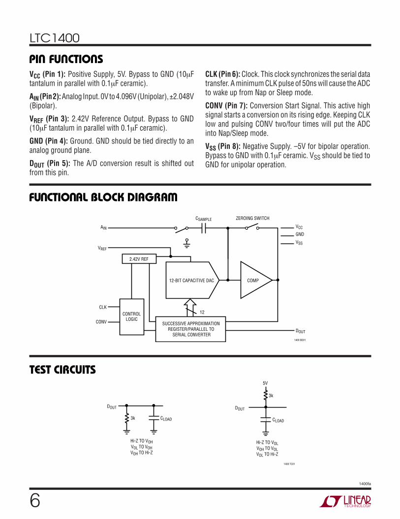
UU WFU CTIO AL BLOCK DIAGRA
1400 BD01
12-BIT CAPACITIVE DAC COMP
SUCCESSIVE APPROXIMATION REGISTER/PARALLEL TO
SERIAL CONVERTER
ZEROING SWITCH
CONTROLLOGIC
2.42V REF
DOUT
VCC
CONV
CLK
VREF
AIN
CSAMPLE
12
GND
VSS
1400 TC01
DOUT DOUT
3k
3k
CLOAD CLOAD
Hi-Z TO VOHVOL TO VOHVOH TO Hi-Z
Hi-Z TO VOLVOH TO VOLVOL TO Hi-Z
5V
TEST CIRCUITS
PI FU CTIO S
UUU
VCC (Pin 1): Positive Supply, 5V. Bypass to GND (10μF tantalum in parallel with 0.1μF ceramic).
AIN (Pin 2): Analog Input. 0V to 4.096V (Unipolar), ±2.048V (Bipolar).
VREF (Pin 3): 2.42V Reference Output. Bypass to GND (10μF tantalum in parallel with 0.1μF ceramic).
GND (Pin 4): Ground. GND should be tied directly to an analog ground plane.
DOUT (Pin 5): The A/D conversion result is shifted out from this pin.
CLK (Pin 6): Clock. This clock synchronizes the serial data transfer. A minimum CLK pulse of 50ns will cause the ADC to wake up from Nap or Sleep mode.
CONV (Pin 7): Conversion Start Signal. This active high signal starts a conversion on its rising edge. Keeping CLK low and pulsing CONV two/four times will put the ADC into Nap/Sleep mode.
VSS (Pin 8): Negative Supply. –5V for bipolar operation. Bypass to GND with 0.1μF ceramic. VSS should be tied to GND for unipolar operation.

LTC1400
71400fa
APPLICATIO S I FOR ATIO
WU UU
Conversion Details
The LTC1400 uses a successive approximation algorithm and an internal sample-and-hold circuit to convert an analog signal to a 12-bit serial output based on a preci-sion internal reference. The control logic provides easy interface to microprocessors and DSPs through 3-wire connections.
A rising edge on the CONV input starts a conversion. At the start of a conversion the successive approximation register (SAR) is reset. Once a conversion cycle has begun it cannot be restarted.
During conversion, the internal 12-bit capacitive DAC output is sequenced by the SAR from the most significant bit (MSB) to the least significant bit (LSB). Referring to Figure 1, the AIN input connects to the sample-and-hold capacitor during the acquired phase and the comparator offset is nulled by the feedback switch. In this acquire phase, it typically takes 200ns for the sample-and-hold capacitor to acquire the analog signal. During the convert phase, the comparator feedback switch opens, putting the comparator into the compare mode. The input switches connect CSAMPLE to ground, injecting the analog input charge onto the summing junction. This input charge is successively compared with the binary-weighted charges supplied by the capacitive DAC. Bit decisions are made by the high speed comparator. At the end of a conversion, the DAC output balances the AIN input charge. The SAR contents (a 12-bit data word) which represent the input voltage, are output through the serial pin DOUT.
1400 F01
SAMPLE
DOUT
CDAC
VDAC
DAC
AIN
CSAMPLE–
+COMP
SAR
SAMPLE
S1
HOLD
Figure 1. AIN Input
Dynamic Performance
The LTC1400 has excellent high speed sampling capability. FFT (Fast Fourier Transform) test techniques are used to test the ADC’s frequency response, distortion and noise at the rated throughput. By applying a low distortion sine wave and analyzing the digital output using an FFT algorithm, the ADC’s spectral content can be examined for frequencies outside the fundamental. Figure 2a shows a typical LTC1400 FFT plot.
Signal-to-Noise Ratio
The signal-to-noise plus distortion ratio [S/(N + D)] is the ratio between the RMS amplitude of the fundamental input frequency to the RMS amplitude of all other frequency components at the A/D output. The output is band limited to frequencies from DC to half the sampling frequency. Figure 2a shows a typical spectral content with a 400kHz sampling rate and a 100kHz input. The dynamic perfor-mance is excellent for input frequencies up to the Nyquist limit of 200kHz as shown in Figure 2b.
FREQUENCY (kHz)0 40 80 100 140 18020 60 120 160 200
AMPL
ITUD
E (d
B)
1400 F02a
0
–10
–20
–30
–40
–50
–60
–70
–80
–90
–100
–110
–120
fSAMPLE = 400kHzfIN = 94.824kHzSINAD = 72.5dBTHD = –82dB
Figure 2a. LTC1400 Nonaveraged, 4096 Point FFTPlot with 100kHz Input Frequency in Bipolar Mode
Effective Number of Bits
The effective number of bits (ENOBs) is a measurement of the effective resolution of an ADC and is directly related to the S/(N + D) by the equation:
N
S N D=
+( )/ – ..
1 766 02

LTC1400
81400fa
APPLICATIO S I FOR ATIO
WU UU
where N is the effective number of bits of resolution and S/(N + D) is expressed in dB. At the maximum sampling rate of 400kHz, the LTC1400 maintains very good ENOBs up to the Nyquist input frequency of 200kHz (refer to Figure 3).
FREQUENCY (kHz)0 40 80 100 140 18020 60 120 160 200
AMPL
ITUD
E (d
B)
1400 F02b
0
–10
–20
–30
–40
–50
–60
–70
–80
–90
–100
–110
–120
fSAMPLE = 400kHzfIN = 199.121kHzSINAD = 72.1dBTHD = –80dB
Figure 2b. LTC1400 Nonaveraged, 4096 Point FFT Plot with 200kHz Input Frequency in Bipolar Mode
INPUT FREQUENCY (Hz)10k
EFFE
CTIV
E NU
MBE
R OF
BIT
S
SIGNAL/(NOISE + DISTORTION) (dB)
12
11
10
9
8
7
6
5
4
3
2
1
0
74
68
62
56
50
100k 1M
1400 F03
NYQUISTFREQUENCY
fSAMPLE = 400kHz
Figure 3. Effective Bits and Signal-to-Noise +Distortion vs Input Frequency in Bipolar Mode
Total Harmonic Distortion
Total harmonic distortion (THD) is the ratio of the RMS sum of all harmonics of the input signal to the fundamental itself. The out-of-band harmonics alias into the frequency band between DC and half of the sampling frequency. THD is expressed as:
THD
V V V VnV
= + + +…20
2 3 41
2 2 2 2log
where V1 is the RMS amplitude of the fundamental fre-quency and V2 through Vn are the amplitudes of the second through nth harmonics. THD vs input frequency is shown in Figure 4. The LTC1400 has good distortion performance up to the Nyquist frequency and beyond.
INPUT FREQUENCY (Hz)10k
AMPL
ITUD
E (d
B BE
LOW
THE
FUN
DAM
ENTA
L) 0
–10
–20
–30
–40
–50
–60
–70
–80
–90
–100100k 1M
1400 F04
2ND HARMONIC
THD3RD HARMONIC
fSAMPLE = 400kHz
Intermodulation Distortion
If the ADC input signal consists of more than one spectral component, the ADC transfer function nonlinearity can produce intermodulation distortion (IMD) in addition to THD. IMD is the change in one sinusoidal input caused by the presence of another sinusoidal input at a different frequency.
If two pure sine waves of frequencies fa and fb are applied to the ADC input, nonlinearities in the ADC transfer func-tion can create distortion products at sum and difference frequencies of mfa ± nfb, where m and n = 0, 1, 2, 3, etc. For example, the 2nd order IMD terms include (fa + fb) and (fa – fb) while the 3rd order IMD terms includes (2fa + fb), (2fa – fb), (fa + 2fb) and (fa – 2fb). If the two input sine waves are equal in magnitude, the value (in decibels) of the 2nd order IMD products can be expressed by the following formula.
IMD fa fb
fa fb±( ) = ±20log
Amplitude at ( )Amplitude at fa
Figure 4. Distortion vs Input Frequency in Bipolar Mode

LTC1400
91400fa
APPLICATIO S I FOR ATIO
WU UU
FREQUENCY (kHz)0 40 80 100 140 18020 60 120 160 200
AMPL
ITUD
E (d
B)
1400 F05
0
–10
–20
–30
–40
–50
–60
–70
–80
–90
–100
–110
–120
fSAMPLE = 400kHzfa = 99.512kHzfb = 102.441kHz
fa fb
3fa2fb – fa2fa + fb
2fa – fb2fb + fa
2fa
3fb
fa + fb
2fbfb – fa
Figure 5. Intermodulation Distortion Plot in Bipolar Mode
Figure 5 shows the IMD performance at a 100kHz input.
Peak Harmonic or Spurious Noise
The peak harmonic or spurious noise is the largest spectral component excluding the input signal and DC. This value is expressed in decibels relative to the RMS value of a full-scale input signal.
Full Power and Full Linear Bandwidth
The full power bandwidth is the input frequency at which the amplitude of the reconstructed fundamental is reduced by 3dB for a full-scale input signal.
The full linear bandwidth is the input frequency at which the S/(N + D) has dropped to 68dB (11 effective bits). The LTC1400 has been designed to optimize input bandwidth, allowing the ADC to undersample input signals with fre-quencies above the converter’s Nyquist Frequency. The noise floor stays very low at high frequencies; S/(N + D) becomes dominated by distortion at frequencies far beyond Nyquist.
Driving the Analog Input
The analog input of the LTC1400 is easy to drive. It draws only one small current spike while charging the sample-and-hold capacitor at the end of a conversion. During conversion, the analog input draws only a small leakage current. The only requirement is that the amplifier driv-ing the analog input must settle after the small current spike before the next conversion starts. Any op amp that
settles in 200ns to small load current transient will allow maximum speed operation. If a slower op amp is used, more settling time can be provided by increasing the time between conversions. Suitable devices capable of driving the ADC’s AIN input include the LT®1360 and the LT1363 op amps.
LTC1400 comes with a built-in unipolar/bipolar detection circuit. If VSS potential is forced below GND, the internal circuitry will automatically switch to bipolar mode.
The following list is a summary of the op amps that are suitable for driving the LTC1400, more detailed informa-tion is available in the Linear Technology databooks or the Linear Technology Website.
LT1215/LT1216: Dual and quad 23MHz, 50V/μs single supply op amps. Single 5V to ±15V supplies, 6.6mA specifications, 90ns settling to 0.5LSB.
LT1223: 100MHz video current feedback amplifier. ±5V to ±15V supplies, 6mA supply current. Low distortion up to and above 400kHz. Low noise. Good for AC applica-tions.
LT1227: 140MHz video current feedback amplifier. ±5V to ±15V supplies, 10mA supply current. Lowest distortion at frequencies above 400kHz. Low noise. Best for AC applications.
LT1229/LT1230: Dual and quad 100MHz current feedback amplifiers. ±2V to ±15V supplies, 6mA supply current each amplifier. Low noise. Good AC specs.
LT1360: 37MHz voltage feedback amplifier. ±5V to ±15V supplies. 3.8mA supply current. Good AC and DC specs. 70ns settling to 0.5LSB.
LT1363: 50MHz, 450V/μs op amps. ±5V to ±15V supplies. 6.3mA supply current. Good AC and DC specs. 60ns settling to 0.5LSB.
LT1364/LT1365: Dual and quad 50MHz, 450V/μs op amps. ±5V to ±15V supplies, 6.3mA supply current per amplifier. 60ns settling to 0.5LSB.
Internal Reference
The LTC1400 has an on-chip, temperature compensated, curvature corrected, bandgap reference, which is factory

LTC1400
101400fa
trimmed to 2.42V. It is internally connected to the DAC and is available at Pin 3 to provide up to 1mA of current to an external load. For minimum code transition noise, the reference output should be decoupled with a capacitor to filter wideband noise from the reference (10μF tantalum in parallel with a 0.1μF ceramic). The VREF pin can be driven with a DAC or other means to provide input span adjust-ment in bipolar mode. The VREF pin must be driven to at least 2.45V to prevent conflict with the internal reference. The reference should not be driven to more than 5V.
Figure 6 shows an LT1360 op amp driving the reference pin. Figure 7 shows a typical reference, the LT1019A-5 connected to the LTC1400. This will provide an improved drift (equal to the maximum 5ppm/°C of the LT1019A-5) and a ±4.231V full scale. If VREF is forced lower than 2.42V, the REFRDY bit in the serial data output will be forced to low.
APPLICATIO S I FOR ATIO
WU UU
1400 F06
–
+VREF(OUT) ≥ 2.45V
AIN
VREF
GND
10µF
3Ω
INPUT RANGE±0.846 • VREF(OUT)
5V
–5V
LTC1400
LT1360
VCC
VSS
Figure 9. LTC1400 Bipolar Transfer Characteristics
Figure 6. Driving the VREF with the LT1360 Op Amp
1400 F07
10µF
3Ω
INPUT RANGE ±4.231V(= ±0.846 • VREF)
–5V
LT1019A-5
10V
VINVOUT
GND
5V
AIN
VREF
GND
LTC1400
VCC
VSS
Figure 7. Supplying a 5V Reference Voltageto the LTC1400 with the LT1019A-5
Unipolar/Bipolar Operation and Adjustment
Figure 8 shows the ideal input/output characteristics for the LTC1400. The code transitions occur midway between successive integer LSB values (i.e., 0.5LSB, 1.5LSB, 2.5LSB, … FS – 1.5LSB). The output code is straight binary with 1LSB = 4.096V/4096 = 1mV. Figure 9 shows the input/output transfer characteristics for the bipolar mode in two’s complement format.
INPUT VOLTAGE (V)
0V
OUTP
UT C
ODE
FS – 1LSB
1400 F08
111...111
111...110
111...101
111...100
000...000
000...001
000...010
000...011
1LSB
UNIPOLARZERO
1LSB = FS4096
Figure 8. LTC1400 Unipolar Transfer Characteristics
INPUT VOLTAGE (V)
0V
OUTP
UT C
ODE
–1 LSB
11400 F09
011...111
011...110
000...001
000...000
100...000
100...001
111...110
1LSB
BIPOLARZERO
111...111
FS/2 – 1LSB–FS/2
Unipolar Offset and Full-Scale Error Adjustments
In applications where absolute accuracy is important, offset and full-scale errors can be adjusted to zero. Figure 10a shows the extra components required for full-scale

LTC1400
111400fa
Figure 10a. LTC1400 Full-Scale Adjust Circuit
1400 F10a
–
+
R210k
R310k
R150Ω
R4100Ω
FULL-SCALEADJUST
VIN
A1
LTC1400
AIN
GND
ADDITIONAL PINS OMITTED FOR CLARITY±20LSB TRIM RANGE
APPLICATIO S I FOR ATIO
WU UU
1400 F10b
–
+R210k
R920Ω
R4100k
R54.3kFULL-SCALE ADJUST
R3100k
R6400Ω
R110k
10k
ANALOGINPUT
0V TO 4.096VA1
5V
R810kOFFSET ADJUST
R7100k
5V
AIN
LTC1400
Figure 10b. LTC1400 Offset and Full-Scale Adjust Circuit
1400 F10c
–
+R210k
R4100k
R54.3kFULL-SCALE ADJUST
R3100k
R6200Ω
R110kANALOG
INPUT±2.048V
A1
R820kOFFSET ADJUST
R7100k
5V
–5V
AIN
LTC1400
Figure 10c. LTC1400 Bipolar Offset and Full-Scale Adjust Circuit
error adjustment. Figure 10b shows offset and full-scale adjustment. Offset error must be adjusted before full-scale error. Zero offset is achieved by applying 0.5mV (i.e., 0.5LSB) at the input and adjusting the offset trim until the LTC1400 output code flickers between 0000 0000 0000 and 0000 0000 0001. For zero full-scale er-ror, apply an analog input of 4.0945V (FS – 1.5LSB or last code transition) at the input and adjust R5 until the LTC1400 output code flickers between 1111 1111 1110 and 1111 1111 1111.
Bipolar Offset and Full-Scale Error Adjustments
Bipolar offset and full-scale errors are adjusted in a similar fashion to the unipolar case. Bipolar offset error adjust-ment is achieved by applying an input voltage of –0.5mV (–0.5LSB) to the input in Figure 10c and adjusting the op amp until the ADC output code flickers between 0000 0000 0000 and 1111 1111 1111. For full-scale adjustment, an input voltage of 2.0465V (FS – 1.5LSBs) is applied to the input and R5 is adjusted until the output code flickers between 0111 1111 1110 and 0111 1111 1111.
Board Layout and Bypassing
To obtain the best performance from the LTC1400, a printed circuit board is required. Layout for the printed circuit board should ensure that digital and analog signal lines are separated as much as possible. In particular, care should be taken not to run any digital track alongside an analog signal track or underneath the ADC. The analog input should be screened by GND.
High quality tantalum and ceramic bypass capacitors should be used at the VCC and VREF pins as shown in the Typical Application on the first page of this data sheet. For the bipolar mode, a 0.1μF ceramic provides adequate bypassing for the VSS pin. For optimum performance, a 10μF surface mount AVX capacitor with a 0.1μF ceramic is recommended for the VCC and VREF pins. The capacitors must be located as close to the pins as possible. The traces connecting the pins and the bypass capacitors must be kept short and should be made as wide as possible. In unipolar mode operation, VSS should be isolated from any noise source before shorting to the GND pin.

LTC1400
121400fa
Input signal leads to AIN and signal return leads from GND (Pin 4) should be kept as short as possible to minimize noise coupling. In applications where this is not possible, a shielded cable between source and ADC is recommended. Also, since any potential difference in grounds between the signal source and ADC appears as an error voltage in series with the input signal, attention should be paid to reducing the ground circuit impedance as much as possible.
APPLICATIO S I FOR ATIO
WU UU
ANALOG SUPPLY
–5V GND 5V
+ +
LTC1400
VSS VCCGND
DIGITAL SUPPLY
GND 5V
+
DIGITAL CIRCUITRY
VCCGND
1400 F11
Figure 11 shows the recommended system ground connec-tions. All analog circuitry grounds should be terminated at
the LTC1400 GND pin. The ground return from the LTC1400 Pin 4 to the power supply should be low impedance for noise free operation. Digital circuitry grounds must be connected to the digital supply common.
In applications where the ADC data outputs and control sig-nals are connected to a continuously active microprocessor bus, it is possible to get errors in the conversion results. These errors are due to feedthrough from the micropro-cessor to the successive approximation comparator. The problem can be eliminated by forcing the microprocessor into a Wait state during conversion or by using three-state buffers to isolate the ADC data bus.
Power-Down Mode
Upon power-up, the LTC1400 is initialized to the active state and is ready for conversion. However, the chip can be easily placed into the Nap or Sleep mode by exercising the right combination of CLK and CONV signal. In the Nap mode all power is off except the internal reference, which is still active and provides 2.42V output voltage to the other circuitry. In this mode, the ADC draws only 6mW of power instead of 75mW (for minimum power, the logic inputs must be within 500mV of the supply rails). The wake-up time from the Nap mode to the active mode is 350ns.
Figure 11. Power Supply Connection
CLK
CONV
NAP
SLEEP
VREF
t1t1
t11 t11
REFRDY
NOTE: NAP AND SLEEP ARE INTERNAL SIGNALS. REFRDY APPEARS AS A BIT IN THE DOUT WORD.
1400 F12
Figure 12. Nap Mode and Sleep Mode Waveforms

LTC1400
131400fa
APPLICATIO S I FOR ATIO
WU UU
In the Sleep mode, power consumption is reduced to a minimum by cutting off the supply to all internal circuitry including the reference. Figure 12 shows the ways to power down the LTC1400. The chip can enter the Nap mode by keeping the CLK signal low and pulsing the CONV signal twice. For Sleep mode operation, CONV signal should be pulsed four times while CLK is kept low.
The LTC1400 can be returned to active mode easily. The rising edge of CLK will wake-up the LTC1400. During the transition from Sleep mode to active mode, the VREF volt-age ramp-up time is a function of the loading conditions. With a 10μF bypass capacitor, the wake-up time from Sleep mode is typically 4ms. A REFRDY signal will be activated once the reference has settled and is ready for an A/D conversion. This REFRDY bit is output to the DOUT pin before the rest of the A/D converted code.
Digital Interface
The digital interface requires only three digital lines. CLK and CONV are both inputs, and the DOUT output provides the conversion result in serial form.
Figure 13 shows the digital timing diagram of the LTC1400 during the A/D conversion. The CONV rising edge starts the conversion. Once initiated, it can not be restarted until the conversion is completed. If the time from CONV signal to CLK rising edge is less than t2, the digital output will be delayed by one clock cycle.
The digital output data is updated on the rising edge of the CLK line. DOUT data should be captured by the receiving system on the rising CLK edge. Data remains valid for a minimum time of t10 after the rising CLK edge to allow capture to occur.
CLK
CONV
INTERNALS/H STATUS
DOUT
t7t31 2 3 4 5 6 7 8 9 10 11 12 13 14 15 1 2
t2
t6
t4 t5
t8
tACQ
SAMPLE SAMPLEHOLD HOLD
Hi-Z Hi-Z
tCONV
tSAMPLE 1400 F13
REFRDY D11 D9 D8 D7 D6 D5 D4 D3 D2 D1 D0D10 REFRDY
Figure 13. ADC Digital Timing Diagram
Figure 14. CLK to DOUT Delay
t10
t8
VIH
VOH
VOL
DOUT
CLK
t9
VIH
90%
10%
DOUT
CLK
1400 F14

LTC1400
141400fa
TYPICAL APPLICATIO S
U
VCC
AIN
VREF
VSS
CLK
CONV
DOUT
GND
TCLKXTCLKRTFSXTFSR
TDRLTC1400
TMS320C50
+10µF 0.1µF
UNIPOLARINPUT
+10µF 0.1µF
5V
1400 TA04a
1
2
3
8 4
6
7
5
Hardware Interface to TMS320C50’s TDM Serial Port (Frame Sync is Generated from TFSX)
Logic Analyzer Waveforms Show 3.2μs Throughput Rate (Input Voltage = 3.046V, Output Code = 1011 1110 0110 = 304610)
Data from LTC1400 Loaded into TMS320C50’s TRCV Register
D0 X XD1D2D4D5 D3RDYX D11 D10 D9 D8 D7 D6
1400 TA05c
D2 D1 D0D3D4D6D7 D500 0 RDY D11 D10 D9 D8
1400 TA05d
Data Stored in TMS320C50’s Memory (in Right Justified Format)

LTC1400
151400fa
THIS PROGRAM DEMONSTRATES LTC1400 INTERFACE TO TMS320C50 FRAME SYNC PULSE IS GENERATED FROM TFSX
*Initialization* .mmregs ; Defines global symbolic names;- - Initialized data memory to zero .ds 0F00h ; Initialize data to zeroDATA0 .word 0 ; Begin sample data locationDATA1 .word 0 ; .DATA2 .word 0 ; Location of dataDATA3 .word 0 ; .DATA4 .word 0 ; .DATA5 .word 0 ; End sample data location;- - Set up the ISR vector .ps 080Ah ; Serial ports interruptsrint : B RECEIVE ; 0A;xint : B TRANSMIT ; 0C;trnt : B TREC ; 0E;txnt : B TTRANX ; 10;;- - Setup the reset vector .ps 0A00h .entrySTART:
*TMS32C050 Initialization* SETC INTM ; Temporarily disable all interrupts LDP #0 ; Set data page pointer to zero OPL #0834h, PMST ; Set up the PMST status and control register LACC #0 SAMM CWSR ; Set software wait state to 0 SAMM PDWSR ;
*Configure Serial Port* SPLK #0038h, TSPC ; Set TDM Serial Port ; TDM = 0 Stand Alone mode ; DLB = 0 Not loop back ; FO = 0 16 Bits ; FSM = 1 Burst Mode ; MCM = 1 CLKX is generated internally ; TXM = 1 FSX as output pin ; Put serial port into reset ; (XRST = RRST =0) SPLK #00F8h, TSPC ; Take Serial Port out of reset ; (XRST = RRST = 1) SPLK #0FFFFh, IFR ; Clear all the pending interrupts
*Start Serial Communication* SACL TDXR ; Generate frame sync pulse SPLK #040h, IMR ; Turn on TRNT receiver interrupt CLRC INTM ; Enable interrupt CLRC SXM ; For Unipolar input, set for right shift ; with no sign extension MAR *AR7 ; Load the auxiliary register pointer with seven LAR AR7, #0F00h ; Load the auxiliary register seven with #0F00h ; as the begin address for data storageWAIT: NOP ; Wait for a receive interrupt NOP ; NOP ; SACL TDXR ; !! regenerate the frame sync pulse B WAIT ;; - - - - - - - end of main program - - - - - - - - - - ;
*Receiver Interrupt Service Routine*TREC: LAMM TRCV ; Load the data received from LTC1400 SFR ; Shift right two times SFR ; AND #1FFFh, 0 ; ANDed with #1FFFh ; For converting the data to right ; justified format ; SACL *+, 0 ; Write to data memory pointed by AR7 and ; increase the memory address by one LACC AR7 ; SUB #0F05h,0 ; Compare to end sample address #0F05h BCND END_TRCV, GEQ ; If the end sample address has exceeded jump to END_TRCV ; SPLK #040h, IMR ; Else Re-enable the TRNT receive interrupt RETE ; Return to main program and enable interrupt
*After Obtained the Data from LTC1400, Program Jump to END_TRCV*END_TRCV: SPLK #002h, IMR ; Enable INT2 for program to halt CLRC INTMSUCCESS: B SUCCESS
*Fill the Unused Interrupt with RETE, to avoid program get “lost”*TTRANX: RETERECEIVE: RETETRANSMIT: RETEINT2: B halt ; Halts the running CPU
TMS320C50 Code for Circuit
TYPICAL APPLICATIO S
U

LTC1400
161400fa
LTC1400 Interface to ADSP2181’s SPORT0 (Frame Sync is Generated from RFS0)
AIN
VSS
VCC
VREF
CLK
CONV
DOUT
GND
SCLKO
RFSO
DR0LTC1400
ADSP2181
UNIPOLARINPUT
+10µF 0.1µF
+10µF
5V
0.1µF
1
2
3
8 4
6
7
5
1400 TA05a
Logic Analyzer Waveforms Show 2.88μs Throughput Rate (Input Voltage = 2.240V, Output Code = 1000 1100 0000 = 224010)
Data from LTC1400 (Normal Mode)
D0 X XD1D2D4D5 D3RDYX D11 D10 D9 D8 D7 D6
1400 TA05c
Data Stored in ADSP2181’s Memory (Normal Mode, SLEN = D)
D2 D1 D0D3D4D6D7 D500 0 RDY D11 D10 D9 D8
1400 TA05d
TYPICAL APPLICATIO S
U

LTC1400
171400fa
THIS PROGRAM DEMONSTRATES LTC1400 INTERFACE TO ADSP-2181 FRAME SYNC PULSE IS GENERATED FROM RFS0
/*Section 1: Initialization*/.module/ram/abs = 0 adspltc; /*define the program module*/ jump start; /*jump over interrupt vectors*/ nop; nop; nop; rti; rti; rti; rti; /*code vectors here upon IRQ2 int*/ rti; rti; rti; rti; /*code vectors here upon IRQL1 int*/ rti; rti; rti; rti; /*code vectors here upon IRQL0 int*/ rti; rti; rti; rti; /*code vectors here upon SPORT0 TX int*/ ax0 = rx0; /*Section 5*/ dm (0x2000) = ax0; /*begin of SPORT0 receive interrupt*/ rti; /* */ /* */ /*end of SPORT0 receive interrupt*/ rti; rti; rti; rti; /*code vectors here upon /IRQE int*/ rti; rti; rti; rti; /*code vectors here upon BDMA interrupt*/ rti; rti; rti; rti; /*code vectors here upon SPORT1 TX (IRQ1) int*/ rti; rti; rti; rti; /*code vectors here upon SPORT1 RX (IRQ0) int*/ rti; rti; rti; rti; /*code vectors here upon TIMER int*/ rti; rti; rti; rti; /*code vectors here upon POWER DOWN int*/
/*Section 2: Configure SPORT0*/start:/*to configure SPORT0 control reg*/ /*SPORT0 address = 0X3FF6*/ /*RFS is used for frame sync generation*/ /*RFS0 is internal, TFS is not use*/ /*bit 0-3 = Slen*/ /*F = 15 = 1111*/ /*E = 14 = 1110*/ /*D = 13 = 1101*/ /*bit 4,5 data type right justified zero filled MSB*/ /*bit 6 INVRFS = 0*/ /*bit 7 INVTFS = 0*/ /*bit 8 IRFS = 1 receive internal frame sync*/ /*bit 9,10,11 are for TFS (don’t care)*/ /*bit 12 TFSW = 1 receive is Normal mode*/ /*bit 13 RTFS = 1 receive is framed mode*/ /*bit 14 ISCLK internal = 1*/ /*bit 15 multichannel mode = 0*/ ax0 = 0x6B0D; /*normal mode, bit12 = 0*/ /*if alternate mode bit12 = 1, ax0 = 0x7F0E*/
dm (0x3FF6) =ax0;
/*Section 3: configure CLKDIV and RFSDIV, setup interrupts*//*to configure CLKDIV reg*/ ax0 = 2; dm(0x3FF5) = ax0; /*set the serial clock divide modulus reg SCLKDIV*/ /*the input clock frequency = 16.67MHz*/ /*CLKOUT frequency = 2x = 33MHz*/ /*SCLK= 1/2*CLKOUT*1/(SCLKDIV+1)*/ /*for SCLKDIV = 2, SCLK = 33/6 = 5.5MHz*//*to Configure RFSDIV*/ ax0 = 15; /*set the RFSDIV reg = 15*/ /*= > the frame sync pulse for every 16 SCLK*/ /*if frame sync pulse in every 15 SCLK, ax0 = 14*/ dm(0x3FF4) = ax0;/*to setup interrupt*/ ifc = 0x0066; /*clear any extraneous SPORT interrupts*/ icntl = 0; /*IRQXB = level sensitivity*/ /*disable nesting interrupt*/ imask= 0x0020; /*bit 0 = timer int = 0*/ /*bit 1 = SPORT1 or IRQ0B int = 0*/ /*bit 2 = SPORT1 or IRQ1B int = 0*/ /*bit 3 = BDMA int = 0*/ /*bit 4 = IRQEB int = 0*/ /*bit 5 = SPORT0 receive int = 1*/ /*bit 6 = SPORT0 transmit int = 0*/ /*bit 7 = IRQ2B int = 0*/ /*enable SPORT0 receive interrupt*/
/*Section 4: Configure System Control Register and Start Communication*//*to configure system control reg*/ ax0 = dm(0x3FFF); /*read the system control reg*/ ay0 = 0xFFF0; ar = ax0 AND ay0; /*set wait state to zero*/ ay0 = 0x1000; ar = ar OR ay0; /*bit12 = 1, enable SPORT0*/ dm(0x3FFF) = ar;/*frame sync pulse regenerated automatically*/ cntr = 5000;do waitloop until ce; nop; nop; nop; nop; nop; nop;waitloop: nop; rts;.endmod;
TYPICAL APPLICATIO S
U
ADSP2181 Code for Circuit

LTC1400
181400fa
TYPICAL APPLICATIO S
U
1 8
LTC1400
CONV
CLK
DOUTGND
ANALOG INPUT(0V TO 4.096V)
12
11
14
13
1512345679
QAQBQCQDQEQFQGQHQH'
D0D1D2D3D4D5D6D7
RCK
SRCK
SER
G
0.1µF
10µF+
10µF
0.1µF
2.42VREFERENCE
OUTPUT +
SRCLR
74HC595
10
12
11
14
13
1512345679
QAQBQCQDQEQFQGQHQH'
D8D9D10D11REFRDY
RCK
SRCK
SER
G
SRCLR
74HC595
10
CLK
CONV
3-WIRE SERIALINTERFACE LINK
5V
1400 TA03
5V
3 VREF
4
2
VCC VSS
AIN
7
6
5
Quick Look Circuit for Converting Data to Parallel Format

LTC1400
191400fa
Information furnished by Linear Technology Corporation is believed to be accurate and reliable. However, no responsibility is assumed for its use. Linear Technology Corporation makes no representa-tion that the interconnection of its circuits as described herein will not infringe on existing patent rights.
BLOCK DIAGRA
W
PACKAGE DESCRIPTIO
U
1 2 3 4
0.150 – 0.157**(3.810 – 3.988)
8 7 6 5
0.189 – 0.197*(4.801 – 5.004)
0.228 – 0.244(5.791 – 6.197)
0.016 – 0.0500.406 – 1.270
0.010 – 0.020(0.254 – 0.508)
× 45°
0°– 8° TYP0.008 – 0.010
(0.203 – 0.254)
SO8 0695
0.053 – 0.069(1.346 – 1.752)
0.014 – 0.019(0.355 – 0.483)
0.004 – 0.010(0.101 – 0.254)
0.050(1.270)
BSCDIMENSION DOES NOT INCLUDE MOLD FLASH. MOLD FLASH SHALL NOT EXCEED 0.006" (0.152mm) PER SIDEDIMENSION DOES NOT INCLUDE INTERLEAD FLASH. INTERLEAD FLASH SHALL NOT EXCEED 0.010" (0.254mm) PER SIDE
*
**
S8 Package8-Lead Plastic Small Outline (Narrow 0.150)
(LTC DWG # 05-08-1610)
Dimensions in inches (millimeters) unless otherwise noted.

LTC1400
201400fa
Linear Technology Corporation1630 McCarthy Blvd., Milpitas, CA 95035-7417 (408) 432-1900 FAX: (408) 434-0507 www.linear.com LINEAR TECHNOLOGY CORPORATION 2006
LT 0606 REV A • PRINTED IN USA
TYPICAL APPLICATIO S
U
RELATED PARTS
VCC
AIN
VREF
VSS
CLK
CONV
DOUT
GND
TCLKXTCLKRTFSXTFSR
TDRLTC1400
TMS320C50
+10µF 0.1µF
UNIPOLARINPUT
+10µF 0.1µF
5V
1400 TA04a
1
2
3
8 4
6
7
5
AIN
VSS
VCC
VREF
CLK
CONV
DOUT
GND
SCLKO
RFSO
DR0LTC1400
ADSP2181
UNIPOLARINPUT
+10µF 0.1µF
+10µF
5V
0.1µF
1
2
3
8 4
6
7
5
1400 TA05a
LTC1400 Interface to ADSP2181
LTC1400 Interface to TMS320C50
PART NUMBER DESCRIPTION COMMENTS
LTC1285/LTC1288 12-Bit, 3V, 7.5/6.6ksps, Micropower Serial ADCs 0.48mW, 1 or 2 Channel Input, SO-8
LTC1286/LTC1298 12-Bit, 5V 12.5/11.16ksps, Micropower Serial ADCs 1.25mW, 1 or 2 Channel Input, SO-8
LTC1290 12-Bit, 50ksps 8-Channel Serial ADC 5V or ± 5V Input Range, 30mW, Full-duplex
LTC1296 12-Bit, 46.5ksps 8-Channel Serial ADC 5V or ± 5V Input Range, 30mW, Half-duplex
LTC1403/LTC1403A 12-/14-Bit, 2.8Msps Serial ADCs 3V, 15mW, MSOP Package
LTC1407/LTC1407A 12-/14-Bit, 3Msps Simultaneous Sampling ADCs 3V, 14mW, 2-Channel Differential Inputs, MSOP Package
LTC1417 14-Bit, 400ksps Serial ADC 5V or ± 5V, 20mW, Internal Reference, SSOP-16
LTC1609 16-Bit, 200ksps Serial ADC 5V, Configurable Bipolar or Unipolar Inputs to ±10V
LTC1860L/LTC1861L 12-Bit, 3V, 150ksps Serial ADCs 1.22mW, 1-/2-Channel Inputs, MSOP and SO-8
LTC1860/LTC1861 12-Bit, 5V, 250ksps Serial ADCs 4.25mW, 1-/2-Channel Inputs, MSOP and SO-8
LTC1864L/LTC1864L 16-Bit, 3V, 150KSPS Serial ADCs 1.22mW, 1-/2-Channel Inputs, MSOP and SO-8
LTC1864/LTC1864 16-Bit, 5V, 250ksps Serial ADCs 4.25mW, 1-/2-Channel Inputs, MSOP and SO-8