Embed Size (px)
Citation preview

LTC3774
13774fb
For more information www.linear.com/LTC3774
Typical applicaTion
FeaTures DescripTion
Dual, Multiphase Current Mode Synchronous Controller for Sub-Milliohm DCR Sensing
The LTC®3774 is a dual PolyPhase® current mode syn-chronous step-down switching regulator controller that drives power blocks, DRMOS or external gate drivers and power MOSFETs. It offers an LTC-proprietary technique that enhances the signal-to-noise ratio of the current sense signal, allowing the use of inductors with very low DC winding resistances as the current sense element for maximum efficiency and reduced jitter.
The maximum current sense voltage is programmable from 10mV to 30mV. High speed, low offset remote sense differential amplifiers and a precise 0.6V reference provide accurate output voltages between 0.6V and 3.5V from a wide 4.5V to 38V input supply range. Soft recovery from output shorts or overcurrent minimizes output overshoot. Burst Mode® operation, continuous and pulse-skipping modes are supported. The constant operating frequency can be synchronized to an external clock or linearly programmed from 200kHz to 1.2MHz. Up to six LTC3774 controllers can be paralleled for 1-, 2-, 3-, 4-, 6-, 8- or 12-phase operation.
The LTC3774 is available in a 36-lead (5mm × 6mm) QFN package.
High Efficiency Dual Phase 1.5V/60A Step-Down Converter
applicaTions
n Sub-Milliohm DCR Current Sensingn Operates with Power Blocks, DRMOS or External
Gate Drivers and MOSFETsn Supports Phase Shedding and N+1 Phase
Redundancyn Programmable DCR Temperature Compensationn ±0.75% Maximum Total DC Output Error Over
Temperaturen Dual Differential Remote Output Voltage Sense
Amplifiersn Phase-Lockable Fixed Frequency Range: 200kHz to
1.2MHzn VIN Range: 4.5V to 38Vn VOUT Range: 0.6V to 3.5Vn Supports Smooth Start-Up into Pre-Biased Outputsn Programmable Soft-Start or VOUT Trackingn Hiccup Mode/Soft Recovery from Output Overcurrent n 36-Lead (5mm × 6mm) QFN Package
n Computer Systemsn Telecom and Datacom Systemsn Industrial Equipmentn DC Power Distribution Systems
L, LT, LTC, LTM, Linear Technology, the Linear logo, PolyPhase and Burst Mode are registered trademarks and No RSENSE and Hot Swap are trademarks of Linear Technology Corporation. All other trademarks are the property of their respective owners. Protected by U.S. Patents, including 5481178, 5705919, 5929620, 6177787, 6580258, 6498466, 6611131, patent pending.
3774 TA01a
VIN4.5V TO 20V
RUN1, 2ILIM1, 2HIZB1HIZB2
PWM1PWMEN1
VOSNS1–
SNSA1+
SNS1–
SNSD1+
VOSNS1+
ITH1
PHSMDCLKOUT
PGOOD1,2MODE/PLLIN
PWM2PWMEN2
GNDVOSNS2
–
SNSA2+
SNS2–
SNSD2+
FREQVOSNS2
+
ITH2
LTC3774
VIN1/4 INTVCC
TK/SS2TK/SS1 INTVCC
37.5k
15k
DRMOS DRMOS
fIN 500kHz
0.33µH(0.32mΩ DCR)
0.33µH(0.32mΩ DCR)
10k300µF
4V330µF
4V15k 0.1µF 4.7µF
2200pF ++
VOUT1.5V60A
22µF50V

LTC3774
23774fb
For more information www.linear.com/LTC3774
pin conFiguraTionabsoluTe MaxiMuM raTings
VIN Voltage ................................................. –0.3V to 40VHIZB Voltage .............................................. –0.3V to 40VRUN, PGOOD, INTVCC Voltage ..................... –0.3V to 6V SNSA1+, SNSA2+, SNSD1+,SNSD2+, SNS1–, SNS2– ........................–0.3V to INTVCCINTVCC Peak Output Current ..................................20mAAll Other Pin Voltages ...........................–0.3V to INTVCCOperating Junction Temperature Range (Note 2) .................................................. –40°C to 125°CStorage Temperature Range .................. –65°C to 150°C
(Note 1)
11 12 13 14
TOP VIEW
37GND
UHE PACKAGE36-LEAD (5mm × 6mm) PLASTIC QFN
15 16 17 18
36 35 34 33 32 31 30 29
21
22
23
24
25
26
27
28
8
7
6
5
4
3
2
1ITEMP2
ITH2
VOSNS2–
VOSNS2+
TK/SS2
HIZB2
PWMEN2
PWM2
RUN2
GND
ITEMP1
ITH1
VOSNS1–
VOSNS1+
TK/SS1
HIZB1
PWMEN1
PWM1
RUN1
GND
ILIM
2
V IN
INTV
CC
CLKO
UT
MOD
E/PL
LIN
FREQ
PHSM
D
ILIM
1
SNSD
2+
SNS2
–
SNSA
2+
PGOO
D2
PGOO
D1
SNSA
1+
SNS1
–
SNSD
1+
20
19
9
10
TJMAX = 125°C, θJA = 43°C/W
EXPOSED PAD (PIN 37) IS GND, MUST BE SOLDERED TO PCB
orDer inForMaTionLEAD FREE FINISH TAPE AND REEL PART MARKING* PACKAGE DESCRIPTION TEMPERATURE RANGE
LTC3774EUHE#PBF LTC3774EUHE#TRPBF 3774 36-Lead (5mm × 6mm) Plastic QFN –40°C to 125°C
LTC3774IUHE#PBF LTC3774IUHE#TRPBF 3774 36-Lead (5mm × 6mm) Plastic QFN –40°C to 125°C
Consult LTC Marketing for parts specified with wider operating temperature ranges. *The temperature grade is identified by a label on the shipping container.Consult LTC Marketing for information on nonstandard lead based finish parts.For more information on lead free part marking, go to: http://www.linear.com/leadfree/ For more information on tape and reel specifications, go to: http://www.linear.com/tapeandreel/

LTC3774
33774fb
For more information www.linear.com/LTC3774
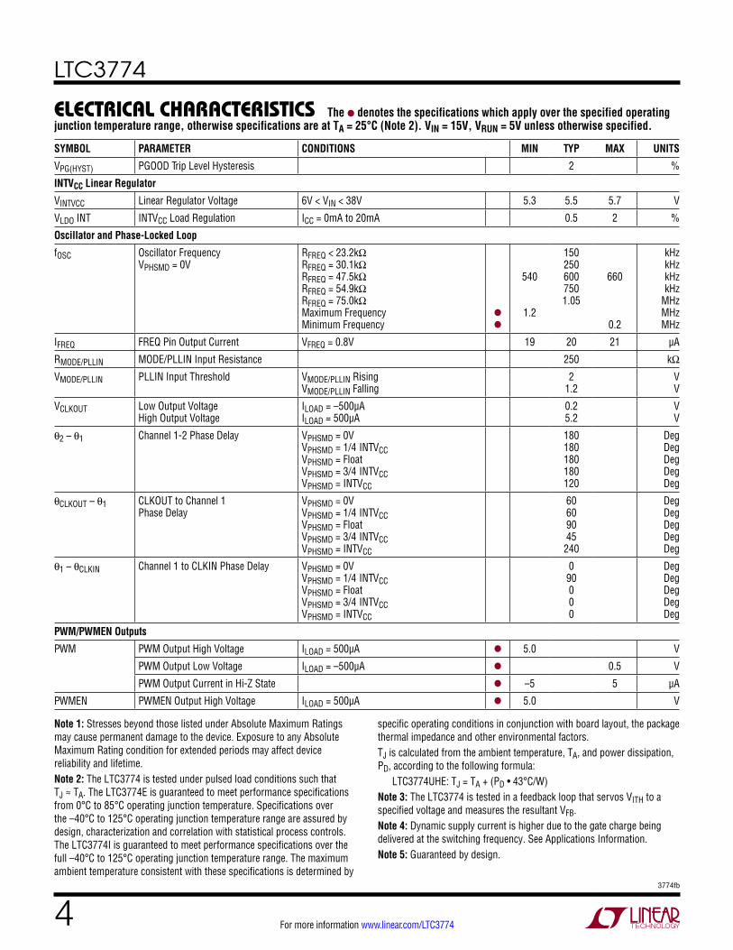
elecTrical characTerisTics The l denotes the specifications which apply over the specified operating junction temperature range, otherwise specifications are at TA = 25°C (Note 2). VIN = 15V, VRUN = 5V unless otherwise specified.
SYMBOL PARAMETER CONDITIONS MIN TYP MAX UNITS
Main Control Loop/Whole System
VIN Input Voltage Range 4.5 38 V
VOUT Output Voltage Range l 0.6 3.5 V
VOSNS+ Regulated Feedback Voltage ITH = 1.2V (Note 3) l 595.5 600 604.5 mV
IOSNS+ Feedback Current –30 –100 nA
VREFLNREG Reference Voltage Line Regulation VIN = 4.5V to 38V 0.002 0.01 %/V
VLOADREG Output Voltage Load Regulation ∆ITH = 1.2V to 0.7V ∆ITH = 1.2V to 1.6V
l
l
0.01 0.01
0.1 0.1
% %
gm Transconductance Amplifier gm ITH = 1.2V, Sink/Source 5µA 2 mmho
f0dB DA Unity-Gain Crossover Frequency (Note 5) 4 MHz
VOVL Feedback Overvoltage Lockout Measured at VOSNS+ l 5 7.5 10 %
IQ Input DC Supply Current Normal Mode Shutdown
(Note 4) VRUN = 0V
9
40
60
mA µA
DFMAX Maximum Duty Factor In Dropout 96 98 %
UVLO Undervoltage Lockout VINTVCC Falling 3.5 3.75 4.0 V
UVLOHYS UVLO Hysteresis 500 mV
ISNSA+ Sense Pin Bias Currents VSNSA
+ = 3.3V ±0.5 ±2 µA
ISNSD+ Sense Pin Bias Currents VSNSD
+ = 3.3V 30 nA
ISNS– Sense Pin Bias Currents VSNS
– = 3.3V 10 µA
AVT_SNS Total Sense Signal Gain to Current Comparator
5 V/V
ITEMP DCR Tempco Compensation Current VITEMP = 0.5V l 27 30 33 µA
ITK/SS Soft-Start Charge Current VTK/SS = 0V l 1 1.25 1.5 µA
tSS(INTERNAL) Internal Soft-Start Time VTK/SS = 5V 600 µs
VHIZB HIZB Pin On Threshold VHIZB Rising 2.2 V
VHIZB_HYS HIZB Pin On Hysteresis 600 mV
VRUN RUN Pin On Threshold VRUN Rising l 1.1 1.22 1.34 V
VRUN_HYS RUN Pin On Hysteresis 80 mV
IRUN RUN Pin Pull-Up Current RUN < On Threshold RUN > On Threshold
RUN < 1.1V RUN > 1.34V
1 5
µA µA
VSENSE(MAX) Maximum Current Sense Threshold ITH = 2V, VSNS– = 3.3V ILIM = 0V ILIM = 1/4 INTVCC ILIM = Float ILIM = 3/4 INTVCC ILIM = INTVCC
l
l
l
l
l
9.25 14 19 24
28.25
10.25
15 20 25
29.75
11.25
16 21 26
31.25
mV mV mV mV mV
Power Good
VPGOOD(ON) PGOOD Pull-Down Resistance 90 200 Ω
IPGOOD(OFF) PGOOD Leakage Current VPGOOD = 5V –2 2 µA
tPGOOD VPGOOD High to Low Delay 45 µs
VPGOOD PGOOD Trip Level VOSNS+ with Respect to Set Output Voltage VOSNS+ Ramping Up VOSNS+ Ramping Down
5
–5
7.5
–7.5
10
–10
% %
LTC3774
43774fb
For more information www.linear.com/LTC3774
elecTrical characTerisTics The l denotes the specifications which apply over the specified operating junction temperature range, otherwise specifications are at TA = 25°C (Note 2). VIN = 15V, VRUN = 5V unless otherwise specified.
SYMBOL PARAMETER CONDITIONS MIN TYP MAX UNITS
VPG(HYST) PGOOD Trip Level Hysteresis 2 %
INTVCC Linear Regulator
VINTVCC Linear Regulator Voltage 6V < VIN < 38V 5.3 5.5 5.7 V
VLDO INT INTVCC Load Regulation ICC = 0mA to 20mA 0.5 2 %
Oscillator and Phase-Locked Loop
fOSC Oscillator Frequency VPHSMD = 0V
RFREQ < 23.2kΩ RFREQ = 30.1kΩ RFREQ = 47.5kΩ RFREQ = 54.9kΩ RFREQ = 75.0kΩ Maximum Frequency Minimum Frequency
l
l
540
1.2
150 250 600 750 1.05
660
0.2
kHz kHz kHz kHz
MHz MHz MHz
IFREQ FREQ Pin Output Current VFREQ = 0.8V 19 20 21 µA
RMODE/PLLIN MODE/PLLIN Input Resistance 250 kΩ
VMODE/PLLIN PLLIN Input Threshold VMODE/PLLIN Rising VMODE/PLLIN Falling
2 1.2
V V
VCLKOUT Low Output Voltage High Output Voltage
ILOAD = –500µA ILOAD = 500µA
0.2 5.2
V V
θ2 – θ1 Channel 1-2 Phase Delay VPHSMD = 0V VPHSMD = 1/4 INTVCC VPHSMD = Float VPHSMD = 3/4 INTVCC VPHSMD = INTVCC
180 180 180 180 120
Deg Deg Deg Deg Deg
θCLKOUT – θ1 CLKOUT to Channel 1 Phase Delay
VPHSMD = 0V VPHSMD = 1/4 INTVCC VPHSMD = Float VPHSMD = 3/4 INTVCC VPHSMD = INTVCC
60 60 90 45
240
Deg Deg Deg Deg Deg
θ1 – θCLKIN Channel 1 to CLKIN Phase Delay VPHSMD = 0V VPHSMD = 1/4 INTVCC VPHSMD = Float VPHSMD = 3/4 INTVCC VPHSMD = INTVCC
0 90 0 0 0
Deg Deg Deg Deg Deg
PWM/PWMEN Outputs
PWM PWM Output High Voltage ILOAD = 500µA l 5.0 V
PWM Output Low Voltage ILOAD = –500µA l 0.5 V
PWM Output Current in Hi-Z State l –5 5 µA
PWMEN PWMEN Output High Voltage ILOAD = 500µA l 5.0 V
Note 1: Stresses beyond those listed under Absolute Maximum Ratings may cause permanent damage to the device. Exposure to any Absolute Maximum Rating condition for extended periods may affect device reliability and lifetime.Note 2: The LTC3774 is tested under pulsed load conditions such that TJ ≈ TA. The LTC3774E is guaranteed to meet performance specifications from 0°C to 85°C operating junction temperature. Specifications over the –40°C to 125°C operating junction temperature range are assured by design, characterization and correlation with statistical process controls. The LTC3774I is guaranteed to meet performance specifications over the full –40°C to 125°C operating junction temperature range. The maximum ambient temperature consistent with these specifications is determined by
specific operating conditions in conjunction with board layout, the package thermal impedance and other environmental factors.TJ is calculated from the ambient temperature, TA, and power dissipation, PD, according to the following formula: LTC3774UHE: TJ = TA + (PD • 43°C/W)Note 3: The LTC3774 is tested in a feedback loop that servos VITH to a specified voltage and measures the resultant VFB.Note 4: Dynamic supply current is higher due to the gate charge being delivered at the switching frequency. See Applications Information.Note 5: Guaranteed by design.

LTC3774
53774fb
For more information www.linear.com/LTC3774
Typical perForMance characTerisTics
Input Quiescent Current vs Input Voltage
Shutdown Current vs Input Voltage INTVCC Line Regulation
Oscillator Frequency vs Input Voltage
Maximum Current Sense Threshold vs Common Mode Voltage
Maximum Current Sense Threshold vs Feedback Voltage (Current Foldback)
Current Sense Threshold vs ITH Voltage
COMMON MODE VOLTAGE (V)0
MAX
IMUM
CUR
RENT
SEN
SE T
HRES
HOLD
(mV)
20
25
30
1.5 2 2.5 3
3774 G01
15
10
0.5 1 3.5
5
0
35
INTVCC3/4 INTVCC1/2 INTVCC
1/4 INTVCC0
FEEDBACK VOLTAGE (V)0
MAX
IMUM
CUR
RENT
SEN
SE T
HRES
HOLD
(mV)
20
25
30
0.2 0.3 0.4 0.5
3774 G02
15
10
0.1 0.6
5
0
35
ILIM = 0
ILIM = 1/4 INTVCC
ILIM = 1/2 INTVCC
ILIM = 3/4 INTVCC
ILIM = INTVCC
V(ITH) (V)0
CURR
ENT
SENS
E TH
RESH
OLD
(mV)
20
25
30
0.75 1 1.51.25 1.75
3774 G03
15
10
5
0
0.25 0.5 2
–5
–10
35ILIM = 0ILIM = 1/4 INTVCCILIM = 1/2 INTVCCILIM = 3/4 INTVCCILIM = INTVCC
INPUT VOLTAGE (V)0
QUIE
SCEN
T CU
RREN
T (m
A)
15 20 3025 35
3774 G04
10
8
6
4
5 10 40
2
0
12
INPUT VOLTAGE (V)0
SHUT
DOW
N CU
RREN
T (µ
A)
15 20 3025 35
3774 G05
50
40
30
20
5 10 40
10
0
60
INPUT VOLTAGE (V)0
INTV
CC V
OLTA
GE (V
)
15 20 3025 35
3774 G06
5
4
3
2
5 10 40
1
0
6
INPUT VOLTAGE (V)0
FREQ
UENC
Y (k
Hz)
15 20 3025 35
3774 G07
1000
800
600
400
5 10 40
200
0
1200
23.2kΩ
47.5kΩ
75kΩ
Load Step (Continuous Conduction Mode)
50µs/DIV3774 G08
VOUT = 1.5V50mV/DIV
AC-COUPLED
ILOAD5A-DIV
15A TO 30A
VIN = 12V

LTC3774
63774fb
For more information www.linear.com/LTC3774
Typical perForMance characTerisTics
Power LossTK/SS Pull-Up Current vs Temperature RUN Threshold vs Temperature
Regulated Feedback Voltage vs Temperature
Oscillator Frequency vs Temperature
Undervoltage Lockout Threshold (INTVCC) vs Temperature
Efficiency Power Loss Efficiency
ILOAD (A)0.01
EFFI
CIEN
CY (%
)
10
3774 G09
90
80
60
40
0.1 1 100
20
10
70
50
30
0
100
BURST MODEPULSE-SKIPPINGCCM
VIN = 7VVOUT = 1.5V
ILOAD (A)0.01
POW
ER L
OSS
(W)
10
3774 G10
4.5
4.0
3.0
2.0
0.1 1 100
1.0
0.5
3.5
2.5
1.5
0
5.0
BURST MODEPULSE-SKIPPINGCCM
VIN = 7VVOUT = 1.5V
ILOAD (A)0.01
EFFI
CIEN
CY (%
)
10
3774 G11
90
80
60
40
0.1 1 100
20
10
70
50
30
0
100VIN = 12VVOUT = 1.5V
BURST MODEPULSE-SKIPPINGCCM
ILOAD (A)0.01
POW
ER L
OSS
(W)
10
3774 G12
4.5
4.0
3.0
2.0
0.1 1 100
1.0
0.5
3.5
2.5
1.5
0
5.0
BURST MODEPULSE-SKIPPINGCCM
VIN = 12VVOUT = 1.5V
TEMPERATURE (°C)–50
I TK/
SS (µ
A)
25
3774 G13
1.4
–25 0 50 12575 100 150
1.2
1.1
1.3
1
1.5
TEMPERATURE (°C)–50
RUN
THRE
SHOL
D (V
)
25
3774 G14
1.3
–25 0 50 12575 100 150
1.1
1.0
1.2
0.9
1.4
ON
OFF
TEMPERATURE (°C)–50
REGU
LATE
D FE
EDBA
CK V
OLTA
GE (m
V)
25
3774 G15
603.0
–25 0 50 12575 100 150
600.0
598.5
597.0
601.5
595.5
604.5
TEMPERATURE (°C)–50
FREQ
UENC
Y (k
Hz)
25
3774 G16
625
–25 0 50 12575 100 150
575
550
675
650
525
600
500
700
TEMPERATURE (°C)–50
3.0
UVLO
THR
ESHO
LD (V
)
3.2
3.6
3.8
4.0
5.0
4.4
0 50 75
3774 G17
3.4
4.6
4.8
4.2
–25 25 100 125 150
RISE
FALL

LTC3774
73774fb
For more information www.linear.com/LTC3774
Typical perForMance characTerisTics
Prebiased Output at 0.5V
Quiescent Current vs Temperature Shutdown Current vs Temperature
FREQ Pin Source Current vs Temperature
TEMPERATURE (°C)–50
QUIE
SCEN
T CU
RREN
T (m
A)
25
3774 G18
9.75
–25 0 50 12575 100 150
9.25
9.50
9.00
8.50
8.25
8.75
8.00
10.00
TEMPERATURE (°C)–50
SHUT
DOW
N CU
RREN
T (µ
A)
25
3774 G19
55
–25 0 50 12575 100 150
45
50
40
30
25
35
20
60
TEMPERATURE (°C)–50
FREQ
PIN
CUR
RENT
(µA)
25
3774 G20
–25 0 50 12575 100 150
21.0
20.5
19.5
19.0
20.0
18.5
21.5
50ms/DIV3774 G08
VOUT500mV/DIV
TRACK/SS500mV/DIV

LTC3774
83774fb
For more information www.linear.com/LTC3774
pin FuncTionsPGOOD1, PGOOD2 (Pin 15, Pin 14): Power Good Indica-tor Outputs. Open drain outputs that pull to ground when output voltage is not in regulation.
SNSA1+, SNSA2+ (Pin 16, Pin 13): AC Current Sense Comparator (+) Inputs. This input senses the signal from the output inductor’s DCR with a filter bandwidth of five times larger than the inductor’s L/DCR value.
SNS1–, SNS2– (Pin 17, Pin 12): Negative current Sense Inputs. The negative input of the current comparator is normally connected to the output.
SNSD1+, SNSD2+ (Pin 18, Pin 11): DC Current Sense Comparator (+) Inputs. This input senses the signal from the output inductor’s DCR with a filter bandwidth equal to the inductor’s L/DCR value.
RUN1, RUN2 (Pin 20, Pin 9): Run Control Inputs. A volt-age above 1.22V turns on the IC. There is a 1µA pull-up current on this pin. Once the RUN pin rises above the 1.22V threshold the pull-up increases to 5µA.
PMW1, PWM2 (Pin 21, Pin 8): (Top) Gate Signal Outputs. This signal goes to the PWM or top gate input of the ex-ternal gate driver or integrated driver MOSFET or Power Block. This is a three-state compatible output.
PWMEN1, PWMEN2 (Pin 22, Pin 7): Enable pins for non-three-state compatible drivers. This pin has an internal open-drain pull-up to INTVCC. An external resistor to GND is required. This pin is low when the corresponding PWM pin is high impedance.
HIZB1, HIZB2 (Pin 23, Pin 6): Phase Shedding Input Pins. When this pin is low, the corresponding PWM pin goes high impedance and PWMEN goes low. Tie to INTVCC or VIN to disable this function.
TK/SS1, TK/SS2 (Pin 24, Pin 5): Output Voltage Tracking and Soft-Start Inputs. The voltage ramp rate at this pin sets the voltage ramp rate of the output. A capacitor to ground accomplishes soft-start. This pin has a 1.25µA pull-up current.
VOSNS1+, VOSNS2
+ (Pin 25, Pin 4): Remote Sense Differ-ential Amplifier Non-inverting Inputs. Connect to Feedback divider center tap with the divider across the output load. The remote sense differential amplifier’s output is internally connected to the error amplifier inverting input.
VOSNS1–, VOSNS2
– (Pin 26, Pin 3): Remote Sense Differ-ential Amplifier Inverting inputs. Connect to sense ground at the output load.
ITH1, ITH2 (Pin 27, Pin 2): Current Control Thresholds and Error Amplifier Compensation Points. The current comparator’s threshold increases with the ITH control voltage.
ITEMP1, ITEMP2 (Pin 28, Pin 1): Input of the temperature sensing comparators. Connect this pin to an external NTC resistor placed near the inductors. Floating this pin disables the DCR temperature compensation function.
ILIM1, ILIM2 (Pin 29, Pin 36): Current Comparator Sense Voltage Limit Selection pins.
PHSMD (Pin 30): Phase Mode Pin. This pin selects CH1-CH2 and CH1-CLKOUT phase relationships.
FREQ (Pin 31): Frequency Set/Select Pin. A resistor between this pin and GND sets the switching frequency. This pin sources 20uA.
MODE/PLLIN (Pin 32): Dual Function Pin. Tying this pin to GND, INTVCC or floating it enables forced continuous mode, pulse-skipping mode or Burst Mode operation re-spectively. Applying a clock signal to this pin causes the internal PLL to synchronize the internal oscillator to the clock signal and forces forced continuous mode. The PLL compensation network is integrated on to the IC.
CLKOUT (Pin 33): Clock Output Pin. This pin is used to synchronize other LTC3774s.
INTVCC (Pin 34): Internal 5.5V Regulator Output. The con-trol circuits are powered from this voltage. Decouple this pin to GND with a minimum of 4.7µF low ESR tantalum or ceramic capacitor. This pin is intended to be used as a reference only. Please do not bias other applications off this voltage!
VIN (Pin 35): Main Input Supply. Decouple this pin to GND with a capacitor (0.1µF to 1µF)
GND (Pins 19, 10, Exposed Pad Pin 37): Ground. All small-signal components and compensation components should be connected here. The exposed pad must be soldered to the PCB ground for electrical connection and rated thermal performance.

LTC3774
93774fb
For more information www.linear.com/LTC3774
FuncTional block DiagraM
– + –+ +
SLEEP
INTVCC
0.55V
NOTE: FUNCTIONAL BLOCK DIAGRAM SHOWS 1 CHANNEL ONLY. THE 2 CHANNELS ARE IDENTICAL.
– +
– +
0.5V
SS – +
1.22V
RUN 1.25µAVIN
EA
ITH RCCC1 CSSRUN TK/SS
0.6VREF
SR Q
PHSMD
5.5VREG
ACTIVE CLAMP
OSC
MODE/SYNCDETECT
SLOPE COMPENSATION
UVLO
1R
ITHB
1µA/5µA
FREQ
CLKOUT
MODE/PLLIN ITEMP
0.6V
BURST EN
ILIM
–
+ –
+ICMP IREV
F
–
+
–
+
OV
UV
–
+DIFFAMP
–
+AMP
0.555V
PGOOD
SNS–
SNSA+
PWM
INTVCC
VOSNS–
VOSNS+
SNSD+
3774 BD
GND
0.645V
20k 20k
OV
RUN
ON
FCNT
PLL-SYNC
TEMPSNS
VIN
SNS–
1/2
PWMEN
SWITCHLOGIC
HIZB
INTVCC
LTC3774
103774fb
For more information www.linear.com/LTC3774
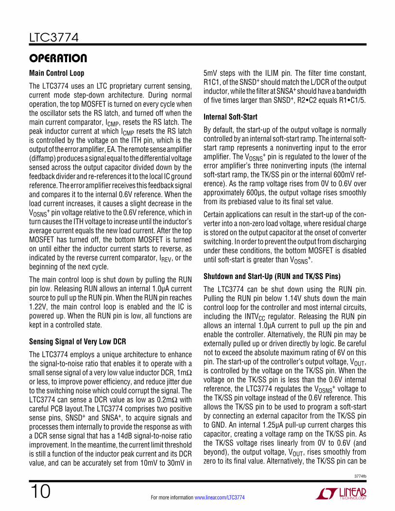
operaTionMain Control Loop
The LTC3774 uses an LTC proprietary current sensing, current mode step-down architecture. During normal operation, the top MOSFET is turned on every cycle when the oscillator sets the RS latch, and turned off when the main current comparator, ICMP , resets the RS latch. The peak inductor current at which ICMP resets the RS latch is controlled by the voltage on the ITH pin, which is the output of the error amplifier, EA. The remote sense amplifier (diffamp) produces a signal equal to the differential voltage sensed across the output capacitor divided down by the feedback divider and re-references it to the local IC ground reference. The error amplifier receives this feedback signal and compares it to the internal 0.6V reference. When the load current increases, it causes a slight decrease in the VOSNS
+ pin voltage relative to the 0.6V reference, which in turn causes the ITH voltage to increase until the inductor’s average current equals the new load current. After the top MOSFET has turned off, the bottom MOSFET is turned on until either the inductor current starts to reverse, as indicated by the reverse current comparator, IREV , or the beginning of the next cycle.
The main control loop is shut down by pulling the RUN pin low. Releasing RUN allows an internal 1.0µA current source to pull up the RUN pin. When the RUN pin reaches 1.22V, the main control loop is enabled and the IC is powered up. When the RUN pin is low, all functions are kept in a controlled state.
Sensing Signal of Very Low DCR
The LTC3774 employs a unique architecture to enhance the signal-to-noise ratio that enables it to operate with a small sense signal of a very low value inductor DCR, 1mΩ or less, to improve power efficiency, and reduce jitter due to the switching noise which could corrupt the signal. The LTC3774 can sense a DCR value as low as 0.2mΩ with careful PCB layout.The LTC3774 comprises two positive sense pins, SNSD+ and SNSA+, to acquire signals and processes them internally to provide the response as with a DCR sense signal that has a 14dB signal-to-noise ratio improvement. In the meantime, the current limit threshold is still a function of the inductor peak current and its DCR value, and can be accurately set from 10mV to 30mV in
5mV steps with the ILIM pin. The filter time constant, R1C1, of the SNSD+ should match the L/DCR of the output inductor, while the filter at SNSA+ should have a bandwidth of five times larger than SNSD+, R2•C2 equals R1•C1/5.
Internal Soft-Start
By default, the start-up of the output voltage is normally controlled by an internal soft-start ramp. The internal soft-start ramp represents a noninverting input to the error amplifier. The VOSNS
+ pin is regulated to the lower of the error amplifier’s three noninverting inputs (the internal soft-start ramp, the TK/SS pin or the internal 600mV ref-erence). As the ramp voltage rises from 0V to 0.6V over approximately 600µs, the output voltage rises smoothly from its prebiased value to its final set value.
Certain applications can result in the start-up of the con-verter into a non-zero load voltage, where residual charge is stored on the output capacitor at the onset of converter switching. In order to prevent the output from discharging under these conditions, the bottom MOSFET is disabled until soft-start is greater than VOSNS
+.
Shutdown and Start-Up (RUN and TK/SS Pins)
The LTC3774 can be shut down using the RUN pin. Pulling the RUN pin below 1.14V shuts down the main control loop for the controller and most internal circuits, including the INTVCC regulator. Releasing the RUN pin allows an internal 1.0µA current to pull up the pin and enable the controller. Alternatively, the RUN pin may be externally pulled up or driven directly by logic. Be careful not to exceed the absolute maximum rating of 6V on this pin. The start-up of the controller’s output voltage, VOUT , is controlled by the voltage on the TK/SS pin. When the voltage on the TK/SS pin is less than the 0.6V internal reference, the LTC3774 regulates the VOSNS
+ voltage to the TK/SS pin voltage instead of the 0.6V reference. This allows the TK/SS pin to be used to program a soft-start by connecting an external capacitor from the TK/SS pin to GND. An internal 1.25µA pull-up current charges this capacitor, creating a voltage ramp on the TK/SS pin. As the TK/SS voltage rises linearly from 0V to 0.6V (and beyond), the output voltage, VOUT , rises smoothly from zero to its final value. Alternatively, the TK/SS pin can be
LTC3774
113774fb
For more information www.linear.com/LTC3774
operaTionused to cause the start-up of VOUT to track that of another supply. Typically, this requires connecting to the TK/SS pin an external resistor divider from the other supply to ground (see the Applications Information section). When the RUN pin is pulled low to disable the controller, or when INTVCC drops below its undervoltage lockout threshold of 3.75V, the TK/SS pin is pulled low by an internal MOSFET. When in undervoltage lockout, the controller is disabled and the external MOSFETs are held off.
Light Load Current Operation (Burst Mode Operation, Pulse-Skipping or Continuous Conduction)
The LTC3774 can be enabled to enter high efficiency Burst Mode operation, constant-frequency pulse-skipping mode or forced continuous conduction mode. To select forced continuous operation, tie the MODE pin to GND. To select pulse-skipping mode of operation, tie the MODE/PLLIN pin to INTVCC. To select Burst Mode operation, float the MODE/PLLIN pin. When the controller is enabled for Burst Mode operation, the peak current in the inductor is set to approximately one-third of the maximum sense voltage even though the voltage on the ITH pin indicates a lower value. If the average inductor current is higher than the load current, the error amplifier, EA, will decrease the voltage on the ITH pin. When the ITH voltage drops below 0.5V, the internal sleep signal goes high (enabling “sleep” mode) and both external MOSFETs are turned off.
In sleep mode, the load current is supplied by the output capacitor. As the output voltage decreases, the EA’s output begins to rise. When the output voltage drops enough, the sleep signal goes low, and the controller resumes normal operation by turning on the top external MOSFET on the next cycle of the internal oscillator. When the controller is enabled for Burst Mode operation, the inductor current is not allowed to reverse. The reverse current comparator (IREV) turns off the bottom external MOSFET just before the inductor current reaches zero, preventing it from re-versing and going negative. Thus, the controller operates in discontinuous operation.
In forced continuous operation, the inductor current is allowed to reverse at light loads or under large transient conditions. The peak inductor current is determined by the voltage on the ITH pin, just as in normal operation. In
this mode, the efficiency at light loads is lower than in Burst Mode operation. However, continuous mode has the advantages of lower output ripple and less interference with audio circuitry.
When the MODE/PLLIN pin is connected to INTVCC, the LTC3774 operates in PWM pulse skipping mode at light loads. At very light loads, the current comparator, ICMP , may remain tripped for several cycles and force the external top MOSFET to stay off for the same number of cycles (i.e., skipping pulses). The inductor current is not allowed to reverse (discontinuous operation). This mode, like forced continuous operation, exhibits low output ripple as well as low audio noise and reduced RF interference as compared to Burst Mode operation. It provides higher low current efficiency than forced continuous mode, but not nearly as high as Burst Mode operation.
Frequency Selection and Phase-Locked Loop (FREQ and MODE/PLLIN Pins)
The selection of switching frequency is a trade-off between efficiency and component size. Low frequency opera-tion increases efficiency by reducing MOSFET switching losses, but requires larger inductance and/or capacitance to maintain low output ripple voltage.
If the MODE/PLLIN pin is not being driven by an external clock source, the FREQ pin can be used to program the controller’s operating frequency from 200kHz to 1.2MHz. There is a precision 20µA current flowing out of the FREQ pin so that the user can program the controller’s switching frequency with a single resistor to GND. A curve is provided later in the Applications Information section showing the relationship between the voltage on the FREQ pin and switching frequency.
A phase-locked loop (PLL) is available on the LTC3774 to synchronize the internal oscillator to an external clock source that is connected to the MODE/PLLIN pin. The PLL loop filter network is integrated inside the LTC3774. The phase-locked loop is capable of locking any frequency within the range of 200kHz to 1.2MHz. The frequency setting resistor should always be present to set the controller’s initial switching frequency before locking to the external clock. The controller operates in forced continuous mode when it is synchronized.

LTC3774
123774fb
For more information www.linear.com/LTC3774
LTC3774
3774 F01a
MODE/PLLIN
PHSMD
+240CLKOUT
LTC3774
0,120 240,60
MODE/PLLIN
PHSMD
CLKOUT
INTVCC
LTC3774
3774 F01b
MODE/PLLIN
PHSMD
+90CLKOUT
LTC3774
0,180 90,270
MODE/PLLIN
PHSMD
CLKOUT
LTC3774
MODE/PLLIN
PHSMD
+60CLKOUT
LTC3774
0,180 60,240
MODE/PLLIN
PHSMD
CLKOUT
3774 F01c
+60
LTC3774
120,300
MODE/PLLIN
PHSMD
CLKOUT
LTC3774
3774 F01d
MODE/PLLIN
PHSMD
+90CLKOUT
LTC3774
135,315
LTC3774
MODE/PLLIN
PHSMD3/4 INTVCC
+45CLKOUT
90,270
LTC3774
MODE/PLLIN
PHSMD
+90CLKOUT
0,180 225,45
MODE/PLLIN
PHSMD
CLKOUT
operaTion
Figure 1a. 3-Phase Operation Figure 1b. 4-Phase Operation
Figure 1c. 6-Phase Operation
Figure 1d. 8-Phase Operation
Figure 1e. 12-Phase Operation
LTC3774
MODE/PLLIN
PHSMD
+60CLKOUT
LTC3774
0,180 60,240
MODE/PLLIN
PHSMD
CLKOUT+60
LTC3774
120,300
MODE/PLLIN
PHSMD
CLKOUT
LTC3774
MODE/PLLIN
PHSMD1/4 INTVCC
+60CLKOUT
LTC3774
150,330 210,30
MODE/PLLIN
PHSMD
CLKOUT
3774 F01e
+60
LTC3774
270,90
MODE/PLLIN
PHSMD
CLKOUT

LTC3774
133774fb
For more information www.linear.com/LTC3774
operaTionMultiphase Operation
For output loads that demand high current, multiple LTC3774s can be daisychained to run out of phase to provide more output current without increasing input and output voltage ripple. The MODE/PLLIN pin allows the LTC3774 to synchronize to the CLKOUT signal of another LTC3774. The CLKOUT signal can be connected to the MODE/PLLIN pin of the following LTC3774 stage to line up both the frequency and the phase of the entire system. Tying the PHSMD pin to INTVCC, GND or floating it generates a phase difference (between CH1 and CLKOUT) of 240°, 60° or 90° respec-tively, and a phase difference (between CH1 and CH2) of 120°, 180° or 180°. Tying PHSMD to 1/4 or 3/4 of INTVCC generates a phase difference of 60° and 45° between CH1 and CLKOUT. Figure 1 shows the PHSMD connections necessary for 3-, 4-, 6-, 8- or 12-phase operation. A total of 12 phases can be daisychained to run simultaneously out of phase with respect to each other.
Sensing the Output Voltage with a Differential Amplifier
The LTC3774 includes a low offset, high input impedance, unity-gain, high bandwidth differential amplifier for ap-plications that require true remote sensing. Sensing the load across the load capacitors directly benefits regulation in high current, low voltage applications, where board interconnection losses can be a significant portion of the total error budget. Connect VOSNS
+ to the center tap of the feedback divider across the output load, and VOSNS
– to the load ground. See Figure 2.
The LTC3774 differential amplifier is configured for unity gain, meaning that the difference between VOSNS
+ and VOSNS
– is translated to its output, relative to GND. The differential amplifier’s output is internally connected to the error amplifier inverting input.
Care should be taken to route the VOSNS+ and VOSNS
– PCB traces parallel to each other all the way to the remote sens-ing points on the board. In addition, avoid routing these sensitive traces near any high speed switching nodes in the circuit. Ideally, the VOSNS
+ and VOSNS– traces should
be shielded by a low impedance ground plane to maintain signal integrity.
Figure 2. Differential Amplifier Connection
LTC3774
FEED
BACK
DIV
IDER
VOSNS+
CF1RD1
COUT1COUT2
VOUT 10Ω
RD2VOSNS
–
3774 F02
10Ω
–
+DIFFAMP

LTC3774
143774fb
For more information www.linear.com/LTC3774
operaTionPower Good (PGOOD Pin)
The PGOOD pin is connected to the open drain of an inter-nal N-channel MOSFET. The MOSFET turns on and pulls the PGOOD pin low when the VOSNS
+ pin voltage is not within ±7.5% of the 0.6V reference voltage. The PGOOD pin is also pulled low when the RUN pin is below 1.14V or when the LTC3774 is in the soft-start or tracking up phase. When the VOSNS
+ pin voltage is within the ±7.5% regulation window, the MOSFET is turned off and the pin is allowed to be pulled up by an external resistor to a source of up to 6V. The PGOOD pin will flag power good immediately when the VOSNS
+ pin is within the regulation window. However, there is an internal 45µs power-bad mask when the VOSNS
+ goes out of the window.
Output Overvoltage Protection
An overvoltage comparator, OV, guards against transient overshoots (>7.5%) as well as other more serious condi-tions that may overvoltage the output. In such cases, the top MOSFET is turned off and the bottom MOSFET is turned on until the overvoltage condition is cleared.
Undervoltage Lockout
The LTC3774 has two functions that help protect the controller in case of undervoltage conditions. A precision UVLO comparator constantly monitors the INTVCC voltage to ensure that an adequate gate-drive voltage is present. It locks out the switching action when INTVCC is below 3.75V. To prevent oscillation when there is a disturbance on the INTVCC, the UVLO comparator has 500mV of preci-sion hysteresis.
Another way to detect an undervoltage condition is to monitor the VIN supply. Because the RUN pin has a preci-sion turn-on reference of 1.22V, one can use a resistor divider to VIN to turn on the IC when VIN is high enough. An extra 4µA of current flows out of the RUN pin once the RUN pin voltage passes 1.22V. The RUN comparator itself has about 80mV of hysteresis. One can program additional hysteresis for the RUN comparator by adjusting the values of the resistive divider. For accurate VIN undervoltage detection, VIN needs to be higher than 4.75V. Always set the VIN undervoltage detection threshold higher than the power stage UVLO threshold so that the LTC3774 is enabled after the power stage is.

LTC3774
153774fb
For more information www.linear.com/LTC3774
applicaTions inForMaTionThe Typical Application on the first page of this data sheet is a basic LTC3774 application circuit. The LTC3774 is designed and optimized for use with a very low DCR value by utilizing a novel approach to reduce the noise sensitivity of the sensing signal by a factor of 14dB. DCR sensing is becoming popular because it saves expensive current sensing resistors and is more power efficient, especially in high current applications. However, as the DCR value drops below 1mΩ, the signal-to-noise ratio is low and current sensing is difficult. LTC3774 uses an LTC proprietary technique to solve this issue. In general, external component selection is driven by the load require-ment, and begins with the DCR and inductor value. Next, power MOSFETs are selected. Finally, input and output capacitors are selected.
Current Limit Programming
The ILIM pin is a 5-level logic input which sets the maxi-mum current limit of the controller. When ILIM is either grounded, floated or tied to INTVCC, the typical value for the maximum current sense threshold will be 10mV, 20mV or 30mV, respectively. Setting ILIM to one-fourth INTVCC and three-fourths INTVCC for maximum current sense thresholds of 15mV and 25mV. Setting ILIM using a resistor divider off of INTVCC will allow the maximum current sense threshold setting to not change when the 5.5V LDO is in dropout at start-up. Please note that the ILIM pin has an internal 500k pull-down to GND and a 500k pull-up to INTVCC.
Which setting should be used? For the best current limit accuracy, use the highest setting that is applicable to the output requirements.
SNSD+, SNSA+ and SNS– Pins
The SNSA+ and SNS– pins are the inputs to the current comparators, while the SNSD+ pin is the input of an internal amplifier. The operating input voltage range is 0V to 3.5V for all three sense pins. All the positive sense pins that are connected to the current comparator or the amplifier are high impedance with input bias currents of less than 1µA, but there is also a resistance of about 300k from the SNS– pin to ground. The SNS– should be connected directly to VOUT. The SNSD+ pin connects to the filter that has a R1•C1 time constant matched to L/DCR of the inductor. The SNSA+ pin is connected to the second filter with the time constant one-fifth that of R1•C1. Care must be taken not to float these pins during normal operation. Filter components, especially capacitors, must be placed close to the LTC3774, and the sense lines should run close together to a Kelvin con-nection underneath the current sense element (Figure 3). Because the LTC3774 is designed to be used with a very low DCR value to sense inductor current, without proper care, the parasitic resistance, capacitance and inductance will degrade the current sense signal integrity, making the programmed current limit unpredictable. As shown in Figure 4, resistors R1 and R2 are placed close to the output inductor and capacitors C1 and C2 are close to the IC pins to prevent noise coupling to the sense signal.
Figure 3. Sense Lines Placement with Inductor DCR
COUT
TO SENSE FILTER,NEXT TO THE CONTROLLER
INDUCTOR3774 F03

LTC3774
163774fb
For more information www.linear.com/LTC3774
applicaTions inForMaTion
The LTC3774 could also be used like any typical current mode controller by disabling the SNSD+ pin, shorting it to ground. An RSENSE resistor or a RC filter can be used to sense the output inductor signal and connects to the SNSA+ pin. If the RC filter is used, its time constant, R • C, is equaled to L/DCR of the output inductor. In these applications, the current limit, VSENSE (MAX), will be five times larger for the specified ILIM, and the operating voltage range of SNSA+ and SNS– is from 0V to 5.25V.
Inductor DCR Sensing
The LTC3774 is specifically designed for high load current applications requiring the highest possible efficiency; it is capable of sensing the signal of an inductor DCR in the sub milliohm range (Figure 4). The DCR is the DC winding resistance of the inductor’s copper, which is often less than 1mΩ for high current inductors. In high current and low output voltage applications, a conduction loss of a high DCR or a sense resistor will cause a significant reduction in power efficiency. For a specific output requirement, chose the inductor with the DCR that satisfies the maxi-
mum desirable sense voltage, and uses the relationship of the sense pin filters to output inductor characteristics as depicted below.
DCR =VSENSE(MAX)
IMAX + ∆IL2
L/DCR = R1• C1 = 5 • R2 • C2
where:
VSENSE(MAX): Maximum sense voltage for a given ILIM threshold
IMAX: Maximum load current
∆IL: Inductor ripple current
L, DCR: Output inductor characteristics
R1 •C1: Filter time constant of the SNSD+ pin
R2 •C2: Filter time constant of the SNSA+ pin
Figure 4. Inductor DCR Current Sensing
VIN VIN
PWM
ITEMP
RNTC100k
INDUCTOR
DCRL
SNSD+
SNSA+
SNS–
GND
LTC3774VOUT
3774 F04
R1
C1
C2
PLACE C1, C2 NEXT TO ICPLACE R1, R2 NEXT TO INDUCTORR1C1 = 5 • R2C2
RS20k
RITEMP
RP43.2k
R2
LTC4449
5V
VLOGIC
VCC
IN
BOOST
TG
TS
BG

LTC3774
173774fb
For more information www.linear.com/LTC3774
applicaTions inForMaTionTo ensure that the load current will be delivered over the full operating temperature range, the temperature coefficient of DCR resistance, approximately 0.4%/°C, should be taken into account. The LTC3774 features a DCR temperature compensation circuit that uses an NTC temperature sensing resistor for this purpose. See the Inductor DCR Sensing Temperature Compensation section for details.
Typically, C1 and C2 are selected in the range of 0.047µF to 0.47µF. If C1 and C2 are chosen to be 220nF, and an inductor of 330nH with 0.32mΩ DCR is selected, R1 and R2 will be 4.7k and 942Ω respectively. The bias current at SNSD+ and SNSA+ is about 30nA and 500nA respectively, and it causes some small error to the sense signal.
There will be some power loss in R1 and R2 that relates to the duty cycle, and will be the most in continuous mode at the maximum input voltage:
PLOSS R( ) =
VIN(MAX) – VOUT( ) • VOUT
R
Ensure that R1 and R2 have a power rating higher than this value. However, DCR sensing eliminates the conduction loss of a sense resistor; it will provide a better efficiency at heavy loads. To maintain a good signal-to-noise ratio for the current sense signal, using a minimum ∆VSENSE of 2mV for duty cycles less than 40% is desirable. The actual ripple voltage will be determined by the following equation:
∆VSENSE = VOUT
VIN•
VIN – VOUTR1• C1• fOSC
Inductor DCR Sensing Temperature Compensation and the ITEMP Pin
Inductor DCR current sensing provides a lossless method of sensing the instantaneous current. Therefore, it can provide higher efficiency for applications of high output
currents. However, the DCR of the inductor, which is the small amount of DC winding resistance of the copper, typically has a positive temperature coefficient. As the temperature of the inductor rises, its DCR value increases. The current limit of the controller is therefore reduced.
The LTC3774 offers a method to counter this inaccuracy by allowing the user to place an NTC temperature sensing resistor near the inductor to actively correct this error. The ITEMP pin, when left floating, is at a voltage around 5V and DCR temperature compensation is disabled. The ITEMP pin has a constant 30µA precision current flowing out the pin. By connecting an NTC resistor from the ITEMP pin to SGND, the maximum current sense threshold can be varied over temperature according the following equation:
VSENSEMAX(ADJ) = VSENSE(MAX) •
2–VITEMP
2.81.5
where:
VSENSEMAX(ADJ) is the maximum adjusted current sense threshold.
VSENSE(MAX) is the maximum current sense threshold specified in the Electrical Characteristics table. It is typi-cally 30mV, 25mV, 20mV, 15mV or 10mV depending on the setting ILIM pins.
VITEMP is the voltage of the ITEMP pin.
The valid voltage range for DCR temperature compensation on the ITEMP pin is 1.4V to 0.6V, with 1.4V or above being no DCR temperature correction and 0.6V the maximum correction. However, if the duty cycle of the controller is less than 25%, the ITEMP range is extended from 1.4V to 0V.
The NTC resistor has a negative temperature coefficient, meaning its value decreases as temperature rises. The VITEMP voltage, therefore, decreases as temperature

LTC3774
183774fb
For more information www.linear.com/LTC3774
applicaTions inForMaTionincreases and in turn, the VSENSEMAX(ADJ) will increase to compensate the DCR temperature coefficient. The NTC resistor, however, is nonlinear and the user can linear-ize its value by building a resistor network with regular resistors. Consult the NTC manufacturer’s data sheets for detailed information.
Another use for the ITEMP pins, in addition to NTC com-pensated DCR sensing, is adjusting VSENSE(MAX) to values between the nominal values of 10mV, 15mV, 20mV, 25mV and 30mV for a more precise current limit. This is done by applying a voltage less than 1.4V to the ITEMP pin. VSENSE(MAX) will be varied per the previous equation and the same duty cycle limitations will apply. The current limit can be adjusted using this method either with a sense resistor or DCR sensing.
NTC Compensated DCR Sensing
For DCR sensing applications where a more accurate current limit is required, a network consisting of an NTC thermistor placed from the ITEMP pin to ground will provide correction of the current limit over temperature. Figure 4 shows this network. Resistors RS and RP will linearize the impedance the ITEMP pin sees. To implement NTC compensated DCR sensing, design the DCR sense filter network per the same procedure mentioned in the previous selection, except calculate the divider components using the room temperature value of the DCR.
1. Set the ITEMP pin resistance to 46.7k at 25°C. With 30µA flowing out of the ITEMP pin, the voltage on the ITEMP pin will be 1.4V at room temperature. Current limit correction will occur for inductor temperatures greater than 25°C.
2. Calculate the ITEMP pin resistance and the maximum inductor temperature which is typically 100°C. Use the equations:
RITEMP100C = VITEMP100C30µA
VITEMP100C = 1.4V – 4.2IMAX •DCR(MAX)•R2 / R1+R2( ) • 100°C– 25°C( ) •0.4 /100
VSENSE(MAX)
Calculate the values for RP and RS. A simple method is to graph the following RS versus RP equations with RS on the y-axis and RP on the x-axis.
RS = RITEMP25C – RNTC25C || RP
RS = RITEMP100C – RNTC100C || RP
Next, find the value of RP that satisfies both equations which will be the point where the curves intersect. Once RP is known, solve for RS.
The resistance of the NTC thermistor can be obtained from the vendor’s data sheet either in the form of graphs, tabulated data or formulas. The approximate value for the NTC thermistor for a given temperature can be calculated from the following equation:
R = RO •exp B •
1T + 273
–1
TO + 273
where:
R = resistance at temperature T, which is in degrees C
RO = resistance at temperature TO, typically 25°C
B = B-constant of the thermistor.
Figure 5 shows a typical resistance curve for a 100k thermistor and the ITEMP pin network over temperature.
Starting values for the NTC compensation network are listed below:
• NTC RO = 100k
• RS = 20k
• RP = 50k
But, the final values should be calculated using the above equations and checked at 25°C and 100°C.

LTC3774
193774fb
For more information www.linear.com/LTC3774
After determining the components for the temperature compensation network, check the results by plotting IMAX versus inductor temperature using the following equations:
IMAX =VSENSEMAX(ADJ) – ∆VSENSE / 2
DCR(MAX) at 25°C • 1+ TL(MAX) – 25°C( ) •0.4 /100( )where:
VSENSEMAX(ADJ) = VSENSE(MAX) •2.0V –
VITEMP2.8
1.5VITEMP = 30µA • RS +RP ||RNTC( )
Use typical values for VSENSE(MAX).
The resulting current limit should be greater than or equal to IMAX for inductor temperatures between 25°C and 100°C.
These are typical values for the NTC compensation network:
• NTC RO = 100k, B-constant = 3000 to 4000
• RS ≈ 20k
• RP ≈ 50k
Generating the IMAX versus inductor temperature curve plot first using the above values as a starting point and then adjusting the RS and RP values as necessary is another
applicaTions inForMaTionapproach. Figure 6 shows a typical curve of IMAX versus inductor temperature.
The same thermistor network can be used to correct for temperatures less than 25°C. But make sure VITEMP is greater than 0.6V for duty cycles of 25% or more, oth-erwise temperature correction may not occur at elevated ambients. For the most accurate temperature detection, place the thermistors next to the inductor as shown in Figure 7. Take care to keep the ITEMP pin away from the switch nodes.
INDUCTOR TEMPERATURE (°C)
10
RESI
STAN
CE (k
Ω)
100
1000
10000
–40 20 40 60 10080 1201
–20 0
3774 F05
THERMISTOR RESISTANCERO = 100kTO = 25°CB = 4334 FOR 25°C/100°C
RITEMPRS = 20k
RP = 43.2k100k NTC
Figure 5. Resistance Versus Temperature for the ITEMP Pin Network and the 100k NTC
INDUCTOR TEMPERATURE (°C)–40
I MAX
(A)
15
20
25
20 60 120
3774 F06
10
5
0–20 0 40 80 100
CORRECTEDIMAX
NOMINALIMAX
UNCORRECTEDIMAXRS = 20k
RP = 43.2kNTC THERMISTOR: RO = 100k TO = 25°C B = 4334
VOUT RNTC
L1
SW13774 F07
Figure 6. Worst-Case IMAX Versus Inductor Temperature Curve with and without NTC Temperature Compensation
Figure 7. Thermistor Location. Place Thermistor Next to Inductor for Accurate Sensing of the Inductor Temperature, But Keep the ITEMP Pin Away from the Switch Nodes and Gate Drive Traces

LTC3774
203774fb
For more information www.linear.com/LTC3774
applicaTions inForMaTionPre-Biased Output Start-Up
There may be situations that require the power supply to start up with a pre-bias on the output capacitors. In this case, it is desirable to start up without discharging that output pre-bias. The LTC3774 can safely power up into a pre-biased output without discharging it.
The LTC3774 accomplishes this by disabling both the top and bottom MOSFETs until the TK/SS pin voltage and the internal soft-start voltage are above the VOSNS
+ pin volt-age. When VOSNS
+ is higher than TK/SS or the internal soft-start voltage, the error amp output is railed low. The control loop would like to turn the bottom MOSFET on, which would discharge the output. Disabling both top and bottom MOSFETs prevents the pre-biased output voltage from being discharged. When TK/SS and the internal soft-start both cross 500mV or VOSNS
+, whichever is lower, both top and bottom MOSFETs are enabled. If the pre-bias is higher than the OV threshold, the bottom gate is turned on immediately to pull the output back into the regulation window.
Overcurrent Fault Recovery
When the output of the power supply is loaded beyond its preset current limit, the regulated output voltage will col-lapse depending on the load. The output may be shorted to ground through a very low impedance path or it may be a resistive short, in which case the output will collapse partially, until the load current equals the preset current limit. The controller will continue to source current into the short. The amount of current sourced depends on the ILIM pin setting and the VOSNS
+ voltage as shown in the Current Foldback graph in the Typical Performance Characteristics section.
Upon removal of the short, the output soft starts using the internal soft-start, thus reducing output overshoot. In the absence of this feature, the output capacitors would have been charged at current limit, and in applications with minimal output capacitance this may have resulted in output overshoot. Current limit foldback is not disabled during an overcurrent recovery. The load must step below the folded back current limit threshold in order to restart from a hard short.
Phase Shedding/n+1 Redundancy (HIZB Pin)
Unlike the RUN pins, the HIZB pins cause the PWM to enter its high impedance state while not pulling down on ITH or TK/SS. This allows two possibilities: First, one can shed a phase based on load requirements via the HIZB pin. This im-proves low current efficiency in a single output multiphase case by reducing switching losses. Second, for applications that require n+1 redundancy, it is now easy to disconnect a channel with damaged MOSFETs or drivers. When com-bined with a Hot Swap™ controller, such as the LTC4226, the HIZB pin could be connected to the gate of the Hot Swap switch. When a damaged MOSFET triggers the Hot Swap controller, it also disables the corresponding chan-nel’s power stage, disconnecting it. Since ITH and TK/SS are unaffected, it does not affect the rest of the system. The propagation delay from HIZB falling to high impedance on PWM is <200ns.
Inductor Value Calculation
Given the desired input and output voltages, the inductor value and operating frequency, fOSC, directly determine the inductor’s peak-to-peak ripple current:
IRIPPLE = VOUT
VIN
VIN – VOUTfOSC •L
Lower ripple current reduces core losses in the inductor, ESR losses in the output capacitors, and output voltage ripple. Thus, highest efficiency operation is obtained at low frequency with a small ripple current. Achieving this, however, requires a large inductor.
A reasonable starting point is to choose a ripple current that is about 40% of IOUT(MAX). Note that the largest ripple current occurs at the highest input voltage. To guarantee that ripple current does not exceed a specified maximum, the inductor should be chosen according to:
L ≥ VIN – VOUT
fOSC • IRIPPLE•
VOUTVIN

LTC3774
213774fb
For more information www.linear.com/LTC3774
Inductor Core Selection
Once the inductance value is determined, the type of in-ductor must be selected. Core loss is independent of core size for a fixed inductor value, but it is very dependent on inductance selected. As inductance increases, core losses go down. Unfortunately, increased inductance requires more turns of wire and therefore copper losses will increase.
Ferrite designs have very low core loss and are preferred at high switching frequencies, so design goals can con-centrate on copper loss and preventing saturation. Ferrite core material saturates “hard,” which means that induc-tance collapses abruptly when the peak design current is exceeded. This results in an abrupt increase in inductor ripple current and consequent output voltage ripple. Do not allow the core to saturate!
PWM and PWMEN Pins
The PWM pins are three-state compatible outputs, de-signed to drive MOSFET drivers, DrMOSs, etc which do not represent a heavy capacitive load. An external resistor divider may be used to set the voltage to mid-rail while in the high impedance state.
The PWMEN outputs have an open-drain pull-up to INTVCC and require an appropriate external pull-down resistor. This pin is intended to drive the enable pins of the MOS-FET drivers that do not have three-state compatible PWM inputs. PWMEN is low only when PWM is high impedance, and high at any other PWM state.
Power MOSFET and Schottky Diode (Optional) Selection
At least two external power MOSFETs need to be selected: One N-channel MOSFET for the top (main) switch and one or more N-channel MOSFET(s) for the bottom (synchro-nous) switch. The number, type and on-resistance of all MOSFETs selected take into account the voltage step-down ratio as well as the actual position (main or synchronous) in which the MOSFET will be used. A much smaller and much lower input capacitance MOSFET should be used for the top MOSFET in applications that have an output
applicaTions inForMaTionvoltage that is less than one-third of the input voltage. In applications where VIN >> VOUT , the top MOSFETs’ on-resistance is normally less important for overall efficiency than its input capacitance at operating frequencies above 300kHz. MOSFET manufacturers have designed special purpose devices that provide reasonably low on-resistance with significantly reduced input capacitance for the main switch application in switching regulators.
The peak-to-peak MOSFET gate drive levels are set by the internal regulator voltage, VINTVCC, requiring the use of logic-level threshold MOSFETs in most applications. Pay close attention to the BVDSS specification for the MOSFETs as well; many of the logic-level MOSFETs are limited to 30V or less. Selection criteria for the power MOSFETs include the on-resistance, RDS(ON), input capacitance, input voltage and maximum output current. MOSFET input capacitance is a combination of several components but can be taken from the typical gate charge curve included on most data sheets (Figure 8). The curve is generated by forcing a constant input current into the gate of a common source, current source loaded stage and then plotting the gate voltage versus time.
Figure 8. Gate Charge Characteristic
+–
VDS
VIN
3774 F08
VGS
MILLER EFFECT
QIN
a b
CMILLER = (QB – QA)/VDS
VGSV
+
–
The initial slope is the effect of the gate-to-source and the gate-to-drain capacitance. The flat portion of the curve is the result of the Miller multiplication effect of the drain-to-gate capacitance as the drain drops the voltage across the current source load. The upper sloping line is due to the drain-to-gate accumulation capacitance and the gate-to-source capacitance. The Miller charge (the increase in coulombs on the horizontal axis from a to b while the curve is flat) is specified for a given VDS drain voltage, but can be adjusted for different VDS voltages by

LTC3774
223774fb
For more information www.linear.com/LTC3774
applicaTions inForMaTionmultiplying the ratio of the application VDS to the curve specified VDS values. A way to estimate the CMILLER term is to take the change in gate charge from points a and b on a manufacturer’s data sheet and divide by the stated VDS voltage specified. CMILLER is the most important se-lection criteria for determining the transition loss term in the top MOSFET but is not directly specified on MOSFET data sheets. CRSS and COS are specified sometimes but definitions of these parameters are not included. When the controller is operating in continuous mode the duty cycles for the top and bottom MOSFETs are given by:
Main SwitchDuty Cycle = VOUTVIN
Synchronous SwitchDuty Cycle = VIN – VOUTVIN
The power dissipation for the main and synchronous MOSFETs at maximum output current are given by:
PMAIN = VOUTVIN
IMAX( )21+ δ( )RDS(ON) +
VIN( )2 IMAX
2
RDR( ) CMILLER( ) •
1VINTVCC – VTH(MIN)
+ 1VTH(MIN)
• f
PSYNC = VIN – VOUTVIN
IMAX( )21+ δ( )RDS(ON)
where δ is the temperature dependency of RDS(ON), RDR is the effective top driver resistance (approximately 2Ω at VGS = VMILLER), VIN is the drain potential and the change in drain potential in the particular application. VTH(MIN) is the data sheet specified typical gate threshold voltage specified in the power MOSFET data sheet at the specified drain current. CMILLER is the calculated capacitance using the gate charge curve from the MOSFET data sheet and the technique described above.
Both MOSFETs have I2R losses while the topside N-channel equation includes an additional term for transition losses, which peak at the highest input voltage. For VIN < 20V, the high current efficiency generally improves with larger
MOSFETs, while for VIN > 20V, the transition losses rapidly increase to the point that the use of a higher RDS(ON) device with lower CMILLER actually provides higher efficiency. The synchronous MOSFET losses are greatest at high input voltage when the top switch duty factor is low or during a short-circuit when the synchronous switch is on close to 100% of the period.
The term (1 + δ ) is generally given for a MOSFET in the form of a normalized RDS(ON) vs temperature curve, but δ = 0.005/°C can be used as an approximation for low voltage MOSFETs.
An optional Schottky diode across the synchronous MOSFET conducts during the dead time between the con-duction of the two large power MOSFETs. This prevents the body diode of the bottom MOSFET from turning on, storing charge during the dead time and requiring a reverse-recovery period which could cost as much as several percent in effi-ciency. A 2A to 8A Schottky is generally a good compromise for both regions of operation due to the relatively small average current. Larger diodes result in additional transition loss due to their larger junction capacitance.
MOSFET Driver Selection
Gate driver ICs, DrMOSs and power blocks with an interface compatible with the LTC3774's three-state PWM outputs or the LTC3774's PWM/PWMEN outputs can be used. Always enable the power stage first, before the LTC3774 is enabled.
CIN and COUT Selection
In continuous mode, the source current of the top MOSFET is a square wave of duty cycle (VOUT)/(VIN). To prevent large voltage transients, a low ESR capacitor sized for the maximum RMS current of one channel must be used. The maximum RMS capacitor current is given by:
CIN Required IRMS ≈ IMAX
VINVOUT( ) VIN – VOUT( )
1/2
This formula has a maximum at VIN = 2VOUT, where IRMS = IOUT/2. This simple worst-case condition is commonly used for design because even significant deviations do not offer much relief. Note that capacitor manufacturers’ ripple current ratings are often based on only 2000 hours of life.

LTC3774
233774fb
For more information www.linear.com/LTC3774
This makes it advisable to further derate the capacitor, or to choose a capacitor rated at a higher temperature than required. Several capacitors may be paralleled to meet size or height requirements in the design. Due to the high operating frequency of the LTC3774, ceramic capacitors can also be used for CIN. Always consult the manufacturer if there is any question.
Ceramic capacitors are becoming very popular for small designs but several cautions should be observed. X7R, X5R and Y5V are examples of a few of the ceramic materials used as the dielectric layer, and these different dielectrics have very different effect on the capacitance value due to the voltage and temperature conditions applied. Physically, if the capacitance value changes due to applied voltage change, there is a concomitant piezo effect which results in radiating sound! A load that draws varying current at an audible rate may cause an attendant varying input volt-age on a ceramic capacitor, resulting in an audible signal. A secondary issue relates to the energy flowing back into a ceramic capacitor whose capacitance value is being reduced by the increasing charge. The voltage can increase at a considerably higher rate than the constant current being supplied because the capacitance value is decreasing as the voltage is increasing! Nevertheless, ceramic capacitors, when properly selected and used, can provide the lowest overall loss due to their extremely low ESR.
A small (0.1µF to 1µF) bypass capacitor, CIN, between the chip VIN pin and ground, placed close to the LTC3774, is also suggested. A 2.2Ω to 10Ω resistor placed between CIN and VIN pin provides further isolation.
The selection of COUT is driven by the required effective series resistance (ESR). Typically once the ESR require-ment is satisfied the capacitance is adequate for filtering. The steady-state output ripple (∆VOUT) is determined by:
∆VOUT ≈ ∆IRIPPLE ESR + 1
8fCOUT
where f = operating frequency, COUT = output capacitance and ∆IRIPPLE = ripple current in the inductor. The output ripple is highest at maximum input voltage since ∆IRIPPLE increases with input voltage. The output ripple will be less
than 50mV at maximum VIN with ∆IRIPPLE = 0.4IOUT(MAX) assuming:
COUT required ESR < N • RSENSE
and
COUT > 1
8f( ) RSENSE( )The emergence of very low ESR capacitors in small, surface mount packages makes very small physical implementa-tions possible. The ability to externally compensate the switching regulator loop using the ITH pin allows a much wider selection of output capacitor types. The impedance characteristic of each capacitor type is significantly differ-ent than an ideal capacitor and therefore requires accurate modeling or bench evaluation during design. Manufacturers such as Nichicon, Nippon Chemi-Con and Sanyo should be considered for high performance through-hole capacitors. The OS-CON semiconductor dielectric capacitors available from Sanyo and the Panasonic SP surface mount types have a good (ESR)(size) product.
Once the ESR requirement for COUT has been met, the RMS current rating generally far exceeds the IRIPPLE(P-P) require-ment. Ceramic capacitors from AVX, Taiyo Yuden, Murata and TDK offer high capacitance value and very low ESR, especially applicable for low output voltage applications.
In surface mount applications, multiple capacitors may have to be paralleled to meet the ESR or RMS current handling requirements of the application. Aluminum electrolytic and dry tantalum capacitors are both available in surface mount configurations. New special polymer surface mount capacitors offer very low ESR also but have much lower capacitive density per unit volume. In the case of tantalum, it is critical that the capacitors are surge tested for use in switching power supplies. Several excellent choices are the AVX TPS, AVX TPSV, the KEMET T510 series of surface mount tantalums or the Panasonic SP series of surface mount special polymer capacitors available in case heights ranging from 2mm to 4mm. Other capacitor types include Sanyo POSCAP, Sanyo OS-CON, Nichicon PL series and Sprague 595D series. Consult the manufacturers for other specific recommendations.
applicaTions inForMaTion

LTC3774
243774fb
For more information www.linear.com/LTC3774
applicaTions inForMaTionDifferential Amplifier
The LTC3774 has true remote voltage sense capability. The sense connections should be returned from the load, back to the differential amplifier’s inputs through a common, tightly coupled pair of PC traces. The differential amplifier rejects common mode signals capacitively or inductively radiated into the feedback PC traces as well as ground loop disturbances. The LTC3774 diffamp has high input impedance on VOSNS
+ pin. The output of the diffamp con-nects to the inverting input of the error amplifier internally.
Setting Output Voltage
The LTC3774 output voltage is set by an external feed-back resistive divider carefully placed across the output, as shown in Figure 2. The regulated output voltage is determined by:
VOUT = 0.6V • 1+ RD1
RD2
To improve the frequency response, a feedforward ca-pacitor, CF1 , may be used. Great care should be taken to route the VOSNS
+ line away from noise sources, such as the inductor or the SW line.
To minimize the effect of the voltage drop caused by high current flowing through board conductance; connect VOSNS– and VOSNS+ sense lines close to the ground and the load output respectively.
External Soft-Start and Tracking
The LTC3774 has the ability to either soft-start by itself or track the output of another channel or external supply. When the controller is configured to soft-start by itself, a capacitor may be connected to its TK/SS pin or the internal soft-start may be used. The controller is in the shutdown state if its RUN pin voltage is below 1.22V and its TK/SS pin is actively pulled to ground in this shutdown state. If the RUN pin voltage is above 1.22V, the controller powers up. A soft-start current of 1.25µA then starts to charge the TK/SS soft-start capacitor. Note that soft-start or tracking is achieved not by limiting the maximum output current of
the controller but by controlling the output ramp voltage according to the ramp rate on the TK/SS pin. The soft-start or tracking range is defined to be the voltage range from 0V to 0.6V on the TK/SS pin. The total soft-start time can be calculated as:
tSOFTSTART = 0.6 •
CSS1.25µA
Regardless of the mode selected by the MODE/PLLIN pin, the controller always starts in discontinuous mode up to TK/SS = 0.5V. Between TK/SS = 0.5V and 0.565V, it will operate in forced continuous mode and revert to the selected mode once TK/SS > 0.565V. The output ripple is minimized during the 65mV forced continuous mode window, ensuring a clean PGOOD signal. When the chan-nel is configured to track another supply, the feedback voltage of the other supply is duplicated by a resistor divider and applied to the TK/SS pin. Therefore, the volt-age ramp rate on this pin is determined by the ramp rate of the other supply’s voltage. It is only possible to track another supply that is slower than the internal soft-start ramp. Note that the small soft-start capacitor charging current is always flowing, producing a small offset error. To minimize this error, select the tracking resistive divider value to be small enough to make this error negligible. In order to track down another channel or supply after the soft-start phase expires, the LTC3774 is forced into continuous mode of operation as soon as VOSNS
+ is below the power good lower threshold regardless of the setting on the MODE/PLLIN pin. However, the LTC3774 should always be set in forced continuous mode tracking down when there is no load. After TK/SS drops below 0.1V, the controller operates in discontinuous mode.
The LTC3774 allows the user to program how its output ramps up and down by means of the TK/SS pin. Through these pins, the output can be set up to either coincidentally or ratiometrically track another supply’s output, as shown in Figure 9. In the following discussions, VOUT2 refers to the LTC3774’s channel 2 as a slave and VOUT1 refers to channel 1 as a master. To implement the coincident track-ing in Figure 9a, connect an additional resistive divider to VOUT1 and connect its mid-point to the TK/SS pin of the

LTC3774
253774fb
For more information www.linear.com/LTC3774
Figure 9. Two Different Modes of Output Voltage Tracking
Figure 10. Setup and Coincident and Ratiometric Tracking
TIME
(9a) Coincident Tracking
VOUT1
VOUT2
OUTP
UT V
OLTA
GE
VOUT1
VOUT2
TIME 3774 F09
(9b) Ratiometric Tracking
OUTP
UT V
OLTA
GE
R3 R1
R4 R2
R3VOUT2
R4
(10a) Coincident Tracking Setup
TOVOSNS1+PIN
TOTK/SS2
PIN
TOVOSNS2+
PIN
VOUT1R1
R2
R3VOUT2
R4
3774 F10
(10b) Ratiometric Tracking Setup
TOVOSNS1+PIN
TOTK/SS2
PIN
TOVOSNS2+
PIN
VOUT1
applicaTions inForMaTionslave controller. The ratio of this divider should be the same as that of the slave controller’s feedback divider shown in Figure 10a. In this tracking mode, VOUT1 must be set higher than VOUT2. To implement the ratiometric tracking in Figure 9b, the ratio of the VOUT2 divider should be exactly the same as the master controller’s feedback divider shown in Figure 10b . By selecting different resis-tors, the LTC3774 can achieve different modes of tracking including the two in Figure 9.
So which mode should be programmed? While either mode in Figure 9 satisfies most practical applications, some trade-offs exist. The ratiometric mode saves a pair of resistors, but the coincident mode offers better output regulation. Under ratiometric tracking, when the master controller’s output experiences dynamic excursion (under load transient, for example), the slave controller output will be affected as well. For better output regulation, use the coincident tracking mode instead of ratiometric.

LTC3774
263774fb
For more information www.linear.com/LTC3774
applicaTions inForMaTionINTVCC (LDO)
The LTC3774 features a true PMOS LDO that supplies power to INTVCC from the VIN supply. INTVCC powers the LTC3774’s internal circuitry. The LDO regulates the voltage at the INTVCC pin to 5.5V when VIN is greater than 6V. The LDO can supply a peak current of 20mA and must be bypassed to ground with a minimum of 4.7µF ceramic capacitor or low ESR electrolytic capacitor. No matter what type of bulk capacitor is used, an additional 0.1µF ceramic capacitor placed directly adjacent to the INTVCC and GND pins is highly recommended.
For applications where the main input power is 5V, tie the VIN and INTVCC pins together and tie the combined pins to the 5V input with a 1Ω or 2.2Ω resistor as shown in Figure 11 to minimize the voltage drop caused by the gate charge current. This will override the INTVCC linear regulator and will prevent INTVCC from dropping too low due to the dropout voltage.
on-time tON(MIN) of the LTC3774 (≈90ns with power stage), the input voltage and inductor value:
∆IL(SC) = tON(MIN) •
VINL
The resulting short-circuit current is:
ISC =
1/ 3VSENSE(MAX)
RSENSE− 1
2∆IL(SC)
After a short, or while starting, make sure that the load current takes the folded-back current limit into account.
Phase-Locked Loop and Frequency Synchronization
The LTC3774 has a phase-locked loop (PLL) comprised of an internal voltage-controlled oscillator (VCO) and a phase detector. This allows the turn-on of the top MOSFET to be locked to the rising edge of an external clock signal applied to the MODE/PLLIN pin. The phase detector is an edge sensitive digital type that provides zero degrees phase shift between the external and internal oscillators. This type of phase detector does not exhibit false lock to harmonics of the external clock.
The output of the phase detector is a pair of complemen-tary current sources that charge or discharge the internal filter network. There is a precision 20µA current flowing out of the FREQ pin. This allows the user to use a single resistor to GND to set the switching frequency when no external clock is applied to the MODE/PLLIN pin. The internal switch between the FREQ pin and the integrated PLL filter network is on, allowing the filter network to be pre-charged at the same voltage as of the FREQ pin. The relationship between the voltage on the FREQ pin and operating frequency is shown in Figure 12 and specified in the Electrical Characteristics table. If an external clock is detected on the MODE/PLLIN pin, the internal switch mentioned above turns off and isolates the influence of the FREQ pin. Note that the LTC3774 can only be synchronized to an external clock whose frequency is within range of the LTC3774’s internal VCO. A simplified block diagram is shown in Figure 13.
Figure 11. Setup for a 5V Input
RVIN1Ω
CIN
3774 F11
5VCINTVCC4.7µF
+INTVCC
LTC3774
VIN
Fault Conditions: Current Limit and Current Foldback
The LTC3774 includes current foldback to help limit load current when the output is shorted to ground. If the output falls below 50% of its nominal output level, then the maximum sense voltage is progressively lowered from its maximum programmed value to one-third of the maximum value. Foldback current limiting is not disabled during soft-start or tracking up. Under short-circuit condi-tions with very low duty cycles, the LTC3774 will begin cycle skipping in order to limit the short-circuit current. In this situation the bottom MOSFET will be dissipating most of the power but less than in normal operation. The short circuit ripple current is determined by the minimum

LTC3774
273774fb
For more information www.linear.com/LTC3774
Figure 12. Relationship Between Oscillator Frequency and Voltage at the FREQ Pin
Figure 13. Phase-Locked Loop Block Diagram
VFREQ (V)0.4
FREQ
UENC
Y (k
Hz)
900
1100
1300
1.0 1.4
3774 F12
700
500
0.6 0.8 1.2 1.6 1.8
300
100
DIGITALPHASE/
FREQUENCYDETECTOR
VCO
2.4V 5.5V
20µARSET
3774 F13
FREQ
SYNCEXTERNAL
OSCILLATOR
MODE/PLLIN
applicaTions inForMaTion
If the external clock frequency is greater than the inter-nal oscillator’s frequency, fOSC, then current is sourced continuously from the phase detector output, pulling up the filter network. When the external clock frequency is less than fOSC, current is sunk continuously, pulling down the filter network. If the external and internal frequencies are the same but exhibit a phase difference, the current sources turn on for an amount of time corresponding to the phase difference. The voltage on the filter network is adjusted until the phase and frequency of the internal and
external oscillators are identical. At the stable operating point, the phase detector output is high impedance and the filter capacitor CLP holds the voltage.
Typically, the external clock (on the MODE/PLLIN pin) input high threshold is 1.6V, while the input low threshold is 1V.
Using the CLKOUT and PHSMD Pins in Multiphase Applications
The LTC3774 features CLKOUT and PHSMD pins that allow multiple LTC3774 ICs to be daisy chained together in multiphase applications. The clock output signal on the CLKOUT pin can be used to synchronize additional ICs in a 3-, 4-, 6-, 8- or 12-phase power supply solution feeding a single high current output, or even several outputs from the same input supply.
The PHSMD pin is used to adjust the phase relationship between channel 1 and channel 2, as well as the phase relationship between channel 1 and CLKOUT. The phases are calculated relative to zero degrees, defined as the rising edge of PWM1. Refer to the Applications Information section for more details on how to create multiphase applications.
Minimum On-Time Considerations
Minimum on-time, tON(MIN), is the smallest time duration that the LTC3774 is capable of turning on the top MOSFET. It is determined by internal timing delays, power stage timing delays and the gate charge required to turn on the top MOSFET. Low duty cycle applications may approach this minimum on-time limit and care should be taken to ensure that:
tON(MIN) < VOUT
VIN f( )
If the duty cycle falls below what can be accommodated by the minimum on-time, the controller will begin to skip cycles. The output voltage will continue to be regulated, but the voltage ripple and current ripple will increase.

LTC3774
283774fb
For more information www.linear.com/LTC3774
The minimum on-time for the LTC3774 is approximately 90ns, with good PCB layout, minimum 30% inductor current ripple and at least 2mV ripple on the current sense signal. The minimum on-time can be affected by PCB switching noise in the voltage and current loop. As the peak sense voltage decreases the minimum on-time gradually increases This is of particular concern in forced continuous applications with low ripple current at light loads. If the duty cycle drops below the minimum on-time limit in this situation, a significant amount of cycle skipping can occur with correspondingly larger current and voltage ripple.
Efficiency Considerations
The percent efficiency of a switching regulator is equal to the output power divided by the input power times 100%. It is often useful to analyze individual losses to determine what is limiting the efficiency and which change would produce the most improvement. Percent efficiency can be expressed as:
%Efficiency = 100% – (L1 + L2 + L3 + ...)
where L1, L2, etc. are the individual losses as a percent-age of input power.
Although all dissipative elements in the circuit produce losses, four main sources usually account for most of the losses in LTC3774 circuits: 1) IC VIN current, 2) MOSFET driver current, 3) I2R losses, 4) topside MOSFET transi-tion losses.
1. The VIN current is the DC supply current given in the Electrical Characteristics table. VIN current typically results in a small (<0.1%) loss.
2. The MOSFET driver current results from switching the gate capacitance of the power MOSFETs. Each time a MOSFET gate is switched from low to high to low again, a packet of charge dQ moves from the driver supply to ground. The resulting dQ/dt is a current out of the driver supply that is typically much larger than the control circuit current. In continuous mode, IGATECHG = f(QT + QB), where QT and QB are the gate charges of the topside and bottom side MOSFETs.
applicaTions inForMaTion3. I2R losses are predicted from the DC resistances of the
fuse (if used), MOSFET, inductor and current sense re-sistor. In continuous mode, the average output current flows through L and RSENSE, but is chopped between the topside MOSFET and the synchronous MOSFET. If the two MOSFETs have approximately the same RDS(ON), then the resistance of one MOSFET can simply be summed with the resistances of L and RSENSE to obtain I2R losses. For example, if each RDS(ON) = 10mΩ, RL = 10mΩ, RSENSE = 5mΩ, then the total resistance is 25mΩ. This results in losses ranging from 2% to 8% as the output current increases from 3A to 15A for a 5V output, or a 3% to 12% loss for a 3.3V output.
Efficiency varies as the inverse square of VOUT for the same external components and output power level. The combined effects of increasingly lower output voltages and higher currents required by high performance digital systems is not doubling but quadrupling the importance of loss terms in the switching regulator system!
4. Transition losses apply only to the topside MOSFET(s), and become significant only when operating at high input voltages (typically 15V or greater). Transition losses can be estimated from:
Transition Loss = (1.7) VIN2 • IO(MAX) • CRSS • f
Other hidden losses such as copper trace and internal battery resistances can account for an additional 5% to 10% efficiency degradation in portable systems. It is very important to include these system level losses during the design phase. The internal battery and fuse resistance losses can be minimized by making sure that CIN has adequate charge storage and very low ESR at the switching frequency. A 25W supply will typically require a minimum of 20µF to 40µF of capacitance having a maximum of 20mΩ to 50mΩ of ESR. Other losses including Schottky conduction losses during dead time and inductor core losses generally account for less than 2% total additional loss.

LTC3774
293774fb
For more information www.linear.com/LTC3774
applicaTions inForMaTionChecking Transient Response
The regulator loop response can be checked by looking at the load current transient response. Switching regulators take several cycles to respond to a step in DC (resistive) load current. When a load step occurs, VOUT shifts by an amount equal to ∆ILOAD • ESR, where ESR is the effective series resistance of COUT . ∆ILOAD also begins to charge or discharge COUT generating the feedback error signal that forces the regulator to adapt to the current change and return VOUT to its steady-state value. During this recovery time VOUT can be monitored for excessive overshoot or ringing, which would indicate a stability problem. The availability of the ITH pin not only allows optimization of control loop behavior but also provides a DC-coupled and AC-filtered closed-loop response test point. The DC step, rise time and settling at this test point truly reflects the closed-loop response. Assuming a predominantly second order system, phase margin and/or damping factor can be estimated using the percentage of overshoot seen at this pin. The bandwidth can also be estimated by examining the rise time at the pin. The ITH external components shown in the Typical Application circuit will provide an adequate starting point for most applications. The ITH series RC-CC filter sets the dominant pole-zero loop compensation. The values can be modified slightly (from 0.5 to 2 times their suggested values) to optimize transient response once the final PC layout is done and the particular output capacitor type and value have been determined. The output capacitors need to be selected because the various types and values determine the loop gain and phase. An output current pulse of 20% to 80% of full-load current having a rise time of 1µs to 10µs will produce output voltage and ITH pin waveforms that will give a sense of the overall loop stability without breaking the feedback loop. Placing a power MOSFET directly across the output capacitor and driving the gate with an appropriate signal generator is a practical way to produce a realistic load step condition. The initial output voltage step resulting from the step change
in output current may not be within the bandwidth of the feedback loop, so this signal cannot be used to determine phase margin. This is why it is better to look at the ITH pin signal which is in the feedback loop and is the filtered and compensated control loop response. The gain of the loop will be increased by increasing RC and the bandwidth of the loop will be increased by decreasing CC. If RC is increased by the same factor that CC is decreased, the zero frequency will be kept the same, thereby keeping the phase shift the same in the most critical frequency range of the feedback loop. The output voltage settling behavior is related to the stability of the closed-loop system and will demonstrate the actual overall supply performance. A second, more severe transient is caused by switching in loads with large (>1µF) supply bypass capacitors. The discharged bypass capacitors are effectively put in parallel with COUT , causing a rapid drop in VOUT . No regulator can alter its delivery of current quickly enough to prevent this sudden step change in output voltage if the load switch resistance is low and it is driven quickly. If the ratio of CLOAD to COUT is greater than 1:50, the switch rise time should be controlled so that the load rise time is limited to approximately 25 • CLOAD. Thus a 10µF capacitor would require a 250µs rise time, limiting the charging current to about 200mA.
PC Board Layout Checklist
When laying out the printed circuit board, the following checklist should be used to ensure proper operation of the IC. These items are also illustrated graphically in the layout diagram of Figure 14. Check the following in the PC layout:
1. The INTVCC decoupling capacitor should be placed immediately adjacent to the IC between the INTVCC pin and GND plane. A 1µF ceramic capacitor of the X7R or X5R type is small enough to fit very close to the IC. An additional 4.7µF to 10µF of ceramic, tantalum or other very low ESR capacitance is recommended in order to keep the internal IC supply quiet.

LTC3774
303774fb
For more information www.linear.com/LTC3774
2. Place the feedback divider between the + and – terminals of COUT. Route VOSNS
+ and VOSNS– with minimum PC
trace spacing from the IC to the feedback divider.
3. Are the SNSA+, SNSD+ and SNS– printed circuit traces routed together with minimum PC trace spacing? The filter capacitors between SNSA+, SNSD+ and SNS– should be as close as possible to the pins of the IC.
4. Do the (+) plates of CIN connect to the drain of the topside MOSFET as closely as possible? This capacitor provides the pulsed current to the MOSFET.
5. Keep the switching nodes away from sensitive small-signal nodes (SNSD+, SNSA+, SNS–, VOSNS
+, VOSNS–).
Ideally the PWM and switch nodes printed circuit traces should be routed away and separated from the IC and especially the quiet side of the IC. Separate the high dv/dt traces from sensitive small-signal nodes with ground traces or ground planes.
6. Use a low impedance source such as a logic gate to drive the MODE/PLLIN pin and keep the lead as short as possible.
7. The 47pF to 330pF ceramic capacitor between the ITH pin and signal ground should be placed as close as possible to the IC. Figure 14 illustrates all branch cur-rents in a switching regulator. It becomes very clear after studying the current waveforms why it is critical to keep the high switching current paths to a small physical size. High electric and magnetic fields will radiate from these loops just as radio stations transmit signals. The output capacitor ground should return to the negative terminal of the input capacitor and not share a com-mon ground path with any switched current paths. The left half of the circuit gives rise to the noise generated by a switching regulator. The ground terminations of the synchronous MOSFET and Schottky diode should return to the bottom plate(s) of the input capacitor(s) with a short isolated PC trace since very high switched currents are present. External OPTI-LOOP® compensa-tion allows overcompensation for PC layouts which are not optimized but this is not the recommended design procedure.
applicaTions inForMaTion
Figure 14. Branch Current Waveforms
+RIN
VIN VOUT
CIN
+COUTD1
SW2
SW1
L1
RSENSE
RL
3774 F14
BOLD LINES INDICATE HIGH, SWITCHING CURRENTS. KEEP LINES TO A MINIMUM LENGTH

LTC3774
313774fb
For more information www.linear.com/LTC3774
8. Are the signal and power grounds kept separate? The IC ground pin and the ground return of CINTVCC must return to the combined COUT (–) terminals. The VOSNS
+ and ITH traces should be as short as possible. The path formed by the top N-channel MOSFET, Schottky diode and the CIN capacitor should have short leads and PC trace lengths. The output capacitor (–) terminals should be connected as close as possible to the (–) terminals of the input capacitor by placing the capacitors next to each other and away from the Schottky loop described above.
9. Use a modified “star ground” technique: a low imped-ance, large copper area central grounding point on the same side of the PC board as the input and output capacitors with tie-ins for the bottom of the INTVCC decoupling capacitor, the bottom of the voltage feedback resistive divider and the GND pin of the IC.
Design Example
As a design example of the front page circuit for a two-channel high current regulator, assume VIN = 12V(nominal), VIN = 20V(maximum), VOUT = 1.5V, IMAX = 60A, and f = 400kHz (see front page schematic).
The regulated output voltage is determined by:
VOUT = 0.6V • 1+ RB
RA
Using a 10k 1% resistor from the VFB node to ground, the top feedback resistor is 15k.
The frequency is set by biasing the FREQ pin to 0.75V (see Figure 12).
The inductance value is based on a 35% maximum ripple current assumption (10.5A per phase). The highest value of ripple current occurs at the maximum input voltage:
L = VOUT
f • ∆IL(MAX)1− VOUT
VIN(MAX)
This design will require 0.33µH. The Würth 744301033, 0.32µH inductor is chosen. At the nominal input voltage (12V), the ripple current will be:
∆IL(NOM) = VOUT
f • L1− VOUT
VIN(NOM)
It will have 10A (33%) ripple. The peak inductor current will be the maximum DC value plus one-half the ripple current, or 35A per phase.
The minimum on-time occurs at the maximum VIN, and should not be less than 100ns (includes margin):
tON(MIN) = VOUT
VIN(MAX)f= 1.5V
20V(400kHz)= 187ns
DCR sensing is used in this circuit. If C1 and C2 are chosen to be 220nF, based on the chosen 0.33µH inductor with 0.32mΩ DCR, R1 and R2 can be calculated as:
R1= LDCR •C1
= 4.69k
R2 = LDCR •C2 • 5
= 937Ω
Choose R1 = 4.64k and R2 = 931Ω.
applicaTions inForMaTion

LTC3774
323774fb
For more information www.linear.com/LTC3774
The maximum DCR of the inductor is 0.34mΩ. The VSENSE(MAX) is calculated as:
VSENSE(MAX) = IPEAK • DCRMAX = 12mV
The current limit is chosen to be 15mV. If temperature variation is considered, please refer to Inductor DCR Sensing Temperature Compensation with NTC Thermistor.
The power dissipation on the topside MOSFET can be easily estimated. Choosing an Infineon BSC050NE2LS MOSFET results in: RDS(ON) = 7.1mΩ (max), VMILLER = 2.8V, CMILLER ≅ 108pF. At maximum input voltage with TJ (estimated) = 75°C:
PMAIN = 1.5V20V
30A( )2 1+(0.005)(75°C – 25°C)[ ] •
0.0071Ω( ) + 20V( )2 30A2
2Ω( ) 108pF( ) •
15.5V – 2.8V
+ 12.8V
400kHz( )
= 599mW + 377mW= 976mW / phase
For a 0.32mΩ DCR, a short-circuit to ground will result in a folded back current of:
ISC =
1/ 3( )15mV0.00032Ω
– 12
90ns(20V)0.33µH
= 12.9A / phase
An Infineon BSC010NE2LS, RDS(ON) = 1.1mΩ, is chosen for the bottom FET. The resulting power loss is:
PSYNC = 20V – 1.5V20V
30A( )2 •
1+ 0.005( ) • 75°C – 25°C( ) • 0.0011Ω
PSYNC = 1.14W/phase
CIN is chosen for an equivalent RMS current rating of at least 13.7A. COUT is chosen with an equivalent ESR of 4.5mΩ for low output ripple. The output ripple in continu-ous mode will be highest at the maximum input voltage. The output voltage ripple due to ESR is approximately:
VORIPPLE = RESR (∆IL) = 0.0045Ω • 10A = 45mVP-P
Further reductions in output voltage ripple can be made by placing a 100µF ceramic capacitor across COUT.
applicaTions inForMaTion

LTC3774
333774fb
For more information www.linear.com/LTC3774
Typical applicaTions
3774
TA0
2
ILIM
1PH
SMD
FREQ
MOD
E/PL
LIN
CLKO
UTIN
TVCC
V IN
ILIM
2
ITEMP2ITH2VOSNS2–VOSNS2+TK/SS2HIZB2PWMEN2PWM2RUN2GND
ITEMP1ITH1
VOSNS1–VOSNS1+
TK/SS1HIZB1
PWMEN1PWM1RUN1GND SN
SD1+
SNS1
–SN
SA1+
PGOO
D1PG
OOD2
SNSA
2+SN
S2–
SNSD
2+
LTC3
774
37.4
k
10k
R S1
20k
R NTC
110
0kR P
143
.2k
R S2
20k
R NTC
210
0kR P
243
.2k
1µF
2.2Ω
30.1
k
4.7µ
F10k
V IN
RUN2
RUN1
INTV
CC
220p
F
0.01
µF
22pF
15k
1.5n
F
180µ
F
10k
10k
100k
100k
10k
220p
F1.
5nF
V IN
V IN
0.22
µF
0.22
µF
0.22
µF
0.22
µF
V IN
PHAS
EV S
WH
CGND
PGND
SMOD
DISB
VCIN
VDRV
22µF
2.2µ
F
1Ω
2.2µ
F
5V B
IAS
22µF
10k
V IN
7V T
O 14
V
INTV
CC
INTV
CC
0.22
µFL1
0.33
µH
10k
10k
4.64
k93
1Ω
C OUT
110
0µF
2×
C OUT
233
0µF
3×
1.5V
/30A
V OUT
1
1.2V
/30A
V OUT
2
V IN
PHAS
EV S
WH
CGND
PGND
SMOD
DISB
VCIN
VDRV22
µF
2.2µ
F
1Ω
2.2µ
F
22µF
0.22
µFL2
0.33
µH
10k
10k
4.64
k93
1Ω
22pF
10k
10k
C OUT
310
0µF
2×
0.01
µF
L1, L
2: W
ÜRTH
744
3010
33C O
UT1,
3: M
URAT
A GR
M31
CR60
J107
ME3
9LC O
UT2,
4: S
ANYO
2R5
TPE3
30M
9
5V B
IAS
V IN
+
FDM
F682
0A
FDM
F682
0A
PWM
BOOT
PWM
BOOT
+
C OUT
433
0µF
3×
+
Dual
1.5
V/30
A an
d 1.
2V/3
0A L
TC37
74 C
onve
rter w
ith D
RMOS
and
DCR
Tem
pera
ture
Coe
ffici
ent C
ompe
nsat
ion

LTC3774
343774fb
For more information www.linear.com/LTC3774
Typical applicaTions
3774
TA0
3
ILIM
1PH
SMD
FREQ
MOD
E/PL
LIN
CLKO
UTIN
TVCC
V IN
ILIM
2
ITEMP2ITH2VOSNS2–VOSNS2+TK/SS2HIZB2PWMEN2PWM2RUN2GND
ITEMP1ITH1
VOSNS1–VOSNS1+
TK/SS1HIZB1
PWMEN1PWM1RUN1
GND SNSD
1+SN
S1–
SNSA
1+PG
OOD1
PGOO
D2SN
SA2+
SNS2
–SN
SD2+
LTC3
774
37.4
k
3.01
k
1µF
2.2Ω
4.7µ
F
V IN
RUN1
INTV
CC
330p
F
0.01
µF
22pF
10k
3.3n
F
180µ
F
10k
10k
10k
10k
V IN
V IN
0.22
µF
0.22
µF
0.22
µF
0.22
µF
V IN
PHAS
EV S
WH
CGND
PGND
SMOD
DISB
VCIN
VDRV
22µF
2.2µ
F
1Ω
2.2µ
F
5V B
IAS
22µF
10k
V IN
7V T
O 14
V
INTV
CC
INTV
CC
0.22
µFL1
0.33
µH
10k
10k
4.64
k93
1Ω
C OUT
110
0µF
4×
1.2V
/60A
V OUT
V IN
PHAS
EV S
WH
CGND
PGND
SMOD
DISB
VCIN
VDRV22
µF
2.2µ
F
1Ω
2.2µ
F
22µF
0.22
µFL2
0.33
µH
10k
10k
4.64
k93
1Ω
C OUT
233
0µF
6×
5V B
IAS
V IN
PWM
BOOT
FDM
F682
0A
FDM
F682
0APW
MBO
OT
+
L1, L
2: W
ÜRTH
744
3010
33C O
UT1:
MUR
ATA
GRM
31CR
60J1
07M
E39L
C OUT
2: S
ANYO
2R5
TPE3
30M
9
2-Ph
ase
1.2V
/60A
LTC
3774
Con
verte
r with
DRM
OS

LTC3774
353774fb
For more information www.linear.com/LTC3774
Typical applicaTions2-
Phas
e 1.
2V/6
0A L
TC37
74 C
onve
rter w
ith D
iscr
ete
Driv
ers
with
MOS
FETs
3774
TA0
4
ILIM
1PH
SMD
FREQ
MOD
E/PL
LIN
CLKO
UTIN
TVCC
V IN
ILIM
2
ITEMP2ITH2VOSNS2–VOSNS2+TK/SS2HIZB2PWMEN2PWM2RUN2GND
ITEMP1ITH1
VOSNS1–VOSNS1+
TK/SS1HIZB1
PWMEN1PWM1RUN1
GND SNSD
1+SN
S1–
SNSA
1+PG
OOD1
PGOO
D2SN
SA2+
SNS2
–SN
SD2+
LTC3
774
37.4
k
3.01
k
1µF
2.2Ω
4.7µ
F
V IN
RUN
INTV
CC
330p
F
0.01
µF22pF
10k
3.3n
F
180µ
F
10k
10k
100k
100k
V IN
V IN
0.22
µF
4.7n
F
1µF
0.22
µF
0.22
µF
0.22
nF
0.22
µF
IN V LOG
IC
V CC
BOOS
T
GND BG TS TG
10k
INTV
CCV C
C
V IN
7V T
O 14
V
V IN
INTV
CC
L10.
33µH
LTC4
449
4.64
k93
1Ω
C OUT
14× C O
UT2
330µ
F6×
1.2V
/60A
V OUT
4.64
k93
1Ω
22nF
×2
BSC0
50NE
2LS
BSC0
10NE
2LS
4.7n
F
1µF
0.22
nF
IN V LOG
IC
V CC
BOOS
T
GND BG TS TG
V CC
22nF
×2
BSC0
50NE
2LS
BSC0
10NE
2LS
L20.
33µH
2.2Ω
2.2Ω
LTC4
449
L1, L
2: W
ÜRTH
744
3010
33C O
UT1:
MUR
ATA
GRM
31CR
60J1
07M
E39L
C OUT
2: S
ANYO
2R5
TPE3
30M
9
+
+

LTC3774
363774fb
For more information www.linear.com/LTC3774
package DescripTion
UHE Package36-Lead Plastic QFN (5mm × 6mm)
(Reference LTC DWG # 05-08-1876 Rev Ø)
Please refer to http://www.linear.com/designtools/packaging/ for the most recent package drawings.
5.00 ±0.10
NOTE:1. DRAWING IS NOT A JEDEC PACKAGE OUTLINE2. DRAWING NOT TO SCALE3. ALL DIMENSIONS ARE IN MILLIMETERS
PIN 1TOP MARK(SEE NOTE 6)
1
1020
28
1119
3629
BOTTOM VIEW—EXPOSED PAD
4.50 REF6.00 ±0.10
R = 0.125TYP
0.25 ±0.05
4.60 ±0.10
3.60±0.10
(UHE36) QFN 0410 REV Ø
0.50 BSC
4.60 ±0.05
3.60 ±0.05
0.75 ±0.05
0.00 – 0.050.200 REF
RECOMMENDED SOLDER PAD LAYOUTAPPLY SOLDER MASK TO AREAS THAT ARE NOT SOLDERED
3.50 REF
0.40 ±0.10
0.70 ±0.05
0.50 BSC4.50 REF
3.50 REF
4.10 ±0.05
5.50 ±0.05
5.10 ±0.056.50 ±0.05
0.25 ±0.05
PACKAGEOUTLINE
4. DIMENSIONS OF EXPOSED PAD ON BOTTOM OF PACKAGE DO NOT INCLUDE MOLD FLASH. MOLD FLASH, IF PRESENT, SHALL NOT EXCEED 0.20mm ON ANY SIDE5. EXPOSED PAD SHALL BE SOLDER PLATED6. SHADED AREA IS ONLY A REFERENCE FOR PIN 1 LOCATION ON THE TOP AND BOTTOM OF PACKAGE
PIN 1 NOTCHR = 0.30 TYP OR 0.35 × 45°
CHAMFER
R = 0.10TYP

LTC3774
373774fb
For more information www.linear.com/LTC3774
Information furnished by Linear Technology Corporation is believed to be accurate and reliable. However, no responsibility is assumed for its use. Linear Technology Corporation makes no representa-tion that the interconnection of its circuits as described herein will not infringe on existing patent rights.
revision hisToryREV DATE DESCRIPTION PAGE NUMBER
A 01/14 Replaced Undervoltage Lockout curveRevised Inductor DCR Sensing Temp Comp and NTC Compensated DCR Sensing sections
617, 18
B 07/15 Minor typographical changesChanged INTVCC pin description
3, 4, 6, 98
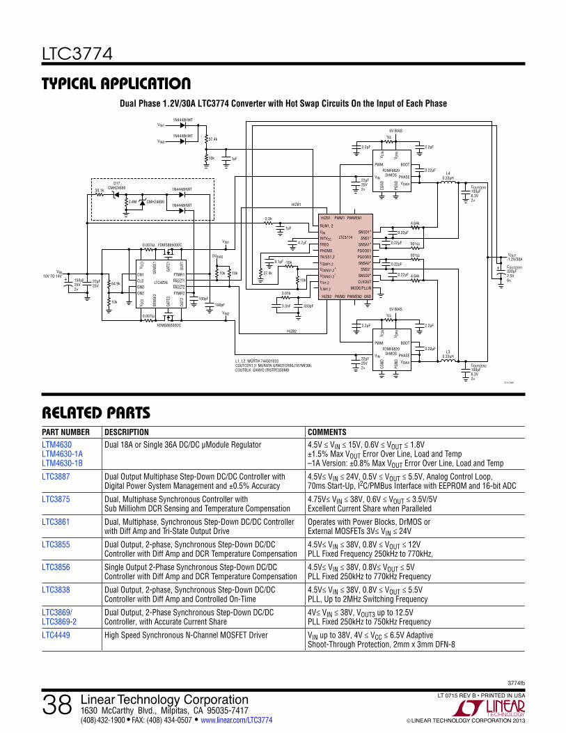
LTC3774
383774fb
For more information www.linear.com/LTC3774 LINEAR TECHNOLOGY CORPORATION 2013
LT 0715 REV B • PRINTED IN USALinear Technology Corporation1630 McCarthy Blvd., Milpitas, CA 95035-7417(408) 432-1900 FAX: (408) 434-0507 www.linear.com/LTC3774
Typical applicaTion
relaTeD parTs
Dual Phase 1.2V/30A LTC3774 Converter with Hot Swap Circuits On the Input of Each Phase
3774 TA05
RUN1, 2
VIN
INTVCC
FREQ
PHSMD
TK/SS1,2
ITEMP1,2
VOSNS1,2+
VOSNS1,2–
ITH1,2
ILIM1,2
ON1
CLS
GND
ON2
FTMR1
FAULT1
FAULT2
FTMR2
SNSD1+
SNS1–
SNSA1+
PGOOD1
PGOOD2
SNSA2+
SNS2–
SNSD2+
CLKOUT
MODE/PLLIN
LTC3774
LTC422664.9k
10k
0.007Ω FDMS86500DC
D17CMHZ4690
0.007Ω
FDMS86500DC
PWM2HIZB2 PWMEN2
PWM1HIZB1
HIZB1
HIZB2
1µF
PWMEN1
GND
4.7µF
10k
0.1µF
37.4k
330pF
L1, L2: WÜRTH 744301033COUTCER1,2: MURATA GRM31CR60J107ME39LCOUTBLK: SANYO 2R5TPE330M9
3.01k
2.2k
3.3nF
10k
V CC2
SENS
E2
GATE
2
OUT2
V CC1
SENS
E1
GATE
1
OUT1
10k 10k
100pF
22µF25V
VIN10V TO 14V
150µF25V2×
5VBIAS
VIN1
VIN2
+
30.1k
100pF
2.4M CMHZ46901N4448HWT
1N4448HWT
PWM
VIN
BOOT
PHASE
VSWH
FDMF6820DrMOS
5V BIAS
1Ω
CGND
PGND
V CIN
V DRV
0.22µFL4
0.33µH
2.2µF
22µF25V2×
2.2µF
0.22µF
0.22µF
0.22µF
0.22µF
931Ω
4.64k
931Ω
4.64k
PWM
VIN
BOOT
PHASE
VSWH
FDMF6820DrMOS
5V BIAS
1Ω
CGND
PGND
V CIN
V DRV
0.22µF
2.2µF
22µF25V2×
2.2µF
COUTCER1100µF6.3V2×
COUTCER1330µF2.5V6×
VOUT1.2V/30A
L30.33µH
COUTCER2100µF6.3V2×
+
1N4448HWT
1N4448HWT
1µF10k
VIN1
VIN237.4k
PART NUMBER DESCRIPTION COMMENTSLTM4630 LTM4630-1A LTM4630-1B
Dual 18A or Single 36A DC/DC μModule Regulator 4.5V ≤ VIN ≤ 15V, 0.6V ≤ VOUT ≤ 1.8V ±1.5% Max VOUT Error Over Line, Load and Temp –1A Version: ±0.8% Max VOUT Error Over Line, Load and Temp
LTC3887 Dual Output Multiphase Step-Down DC/DC Controller with Digital Power System Management and ±0.5% Accuracy
4.5V≤ VIN ≤ 24V, 0.5V ≤ VOUT ≤ 5.5V, Analog Control Loop, 70ms Start-Up, I2C/PMBus Interface with EEPROM and 16-bit ADC
LTC3875 Dual, Multiphase Synchronous Controller with Sub Milliohm DCR Sensing and Temperature Compensation
4.75V≤ VIN ≤ 38V, 0.6V ≤ VOUT ≤ 3.5V/5V Excellent Current Share when Paralleled
LTC3861 Dual, Multiphase, Synchronous Step-Down DC/DC Controller with Diff Amp and Tri-State Output Drive
Operates with Power Blocks, DrMOS or External MOSFETs 3V≤ VIN ≤ 24V
LTC3855 Dual Output, 2-phase, Synchronous Step-Down DC/DC Controller with Diff Amp and DCR Temperature Compensation
4.5V≤ VIN ≤ 38V, 0.8V ≤ VOUT ≤ 12V PLL Fixed Frequency 250kHz to 770kHz,
LTC3856 Single Output 2-Phase Synchronous Step-Down DC/DC Controller with Diff Amp and DCR Temperature Compensation
4.5V≤ VIN ≤ 38V, 0.8V≤ VOUT ≤ 5V PLL Fixed 250kHz to 770kHz Frequency
LTC3838 Dual Output, 2-phase, Synchronous Step-Down DC/DC Controller with Diff Amp and Controlled On-Time
4.5V≤ VIN ≤ 38V, 0.8V ≤ VOUT ≤ 5.5V PLL, Up to 2MHz Switching Frequency
LTC3869/ LTC3869-2
Dual Output, 2-Phase Synchronous Step-Down DC/DC Controller, with Accurate Current Share
4V≤ VIN ≤ 38V, VOUT3 up to 12.5V PLL Fixed 250kHz to 750kHz Frequency
LTC4449 High Speed Synchronous N-Channel MOSFET Driver VIN up to 38V, 4V ≤ VCC ≤ 6.5V Adaptive Shoot-Through Protection, 2mm x 3mm DFN-8