Embed Size (px)
Citation preview
LTC4013
14013fa
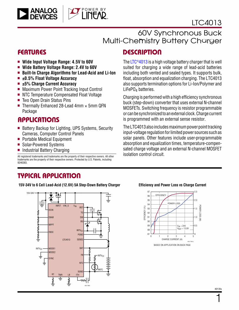
TYPICAL APPLICATION
FEATURES DESCRIPTION
60V Synchronous Buck Multi-Chemistry Battery Charger
The LTC®4013 is a high voltage battery charger that is well suited for charging a wide range of lead-acid batteries including both vented and sealed types. It supports bulk, float, absorption and equalization charging. The LTC4013 also supports termination options for Li-Ion/Polymer and LiFePO4 batteries.
Charging is performed with a high efficiency synchronous buck (step-down) converter that uses external N-channel MOSFETs. Switching frequency is resistor programmable or can be synchronized to an external clock. Charge current is programmed with an external sense resistor.
The LTC4013 also includes maximum power point tracking input-voltage regulation for limited power sources such as solar panels. Other features include user-programmable absorption and equalization times, temperature-compen-sated charge voltage and an external N-channel MOSFET isolation control circuit.
15V-34V to 6 Cell Lead-Acid (12.6V) 5A Step-Down Battery Charger Efficiency and Power Loss vs Charge Current
APPLICATIONS
n Wide Input Voltage Range: 4.5V to 60V n Wide Battery Voltage Range: 2.4V to 60V n Built-In Charge Algorithms for Lead-Acid and Li-Ion n ±0.5% Float Voltage Accuracy n ±5% Charge Current Accuracy n Maximum Power Point Tracking Input Control n NTC Temperature Compensated Float Voltage n Two Open Drain Status Pins n Thermally Enhanced 28-Lead 4mm × 5mm QFN
Package
n Battery Backup for Lighting, UPS Systems, Security Cameras, Computer Control Panels
n Portable Medical Equipment n Solar-Powered Systems n Industrial Battery Charging
All registered trademarks and trademarks are the property of their respective owners. All other trademarks are the property of their respective owners. Protected by U.S. Patents, including 9246383.
INTVCC
INTVCC
15V-34V
DCIN
ENAB
INTVCC
SYNC
SGND
SENSE
BAT
ITHRT
PGND
FB
TG
SW
BST
BG
VIN
FBOC
MPPT
INFET
LB
NTC
MODE1
MODE2
VIN_S
TMR
LTC4013
RNTC
4013 TA01
VIN = 24VVBAT = 13.8V
EFFICIENCY
POWER LOSS
CHARGE CURRENT (A)
BASED ON APPLICATION ON BACK PAGE
0 1 2 3 4 587
88
89
90
91
92
93
94
95
96
97
0
0.5
1.0
1.5
2.0
2.5
EFFI
CIEN
CY (%
)
POWER LOSS (W
)
4013 TA01a
LTC4013
24013fa
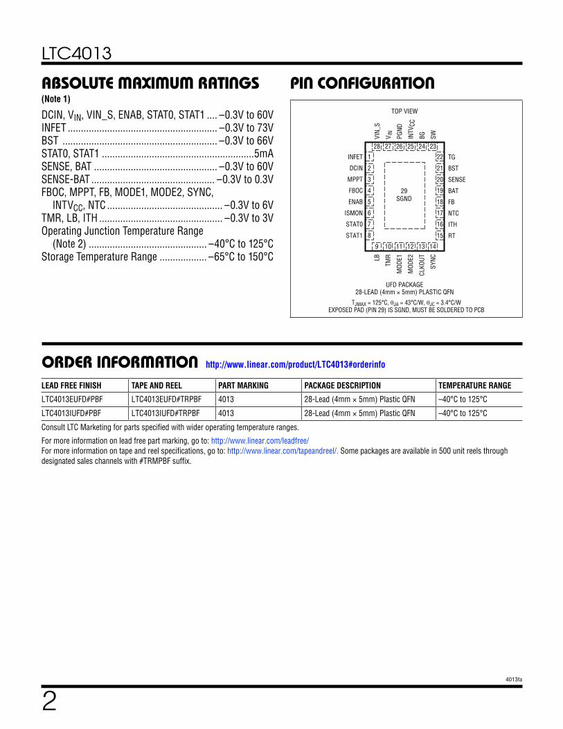
PIN CONFIGURATIONABSOLUTE MAXIMUM RATINGS
DCIN, VIN, VIN_S, ENAB, STAT0, STAT1 .... –0.3V to 60VINFET ......................................................... –0.3V to 73VBST ........................................................... –0.3V to 66VSTAT0, STAT1 ..........................................................5mASENSE, BAT ............................................... –0.3V to 60VSENSE-BAT ............................................... –0.3V to 0.3VFBOC, MPPT, FB, MODE1, MODE2, SYNC,
INTVCC, NTC ............................................ –0.3V to 6VTMR, LB, ITH ............................................... –0.3V to 3VOperating Junction Temperature Range
(Note 2) ............................................. –40°C to 125°CStorage Temperature Range .................. –65°C to 150°C
(Note 1)
9 10
TOP VIEW
UFD PACKAGE28-LEAD (4mm × 5mm) PLASTIC QFN
11 12 13
28 27 26 25 24
14
23
6
5
4
3
2
1INFET
DCIN
MPPT
FBOC
ENAB
ISMON
STAT0
STAT1
TG
BST
SENSE
BAT
FB
NTC
ITH
RT
VIN_
S
V IN
PGND
INTV
CCBG SW
LB
TMR
MOD
E1
MOD
E2
CLKO
UT
SYNC
7
17
18
19
20
21
22
16
8 15
29SGND
TJMAX = 125°C, θJA = 43°C/W, θJC = 3.4°C/W
EXPOSED PAD (PIN 29) IS SGND, MUST BE SOLDERED TO PCB
ORDER INFORMATIONLEAD FREE FINISH TAPE AND REEL PART MARKING PACKAGE DESCRIPTION TEMPERATURE RANGE
LTC4013EUFD#PBF LTC4013EUFD#TRPBF 4013 28-Lead (4mm × 5mm) Plastic QFN –40°C to 125°C
LTC4013IUFD#PBF LTC4013IUFD#TRPBF 4013 28-Lead (4mm × 5mm) Plastic QFN –40°C to 125°C
Consult LTC Marketing for parts specified with wider operating temperature ranges.
For more information on lead free part marking, go to: http://www.linear.com/leadfree/ For more information on tape and reel specifications, go to: http://www.linear.com/tapeandreel/. Some packages are available in 500 unit reels through designated sales channels with #TRMPBF suffix.
http://www.linear.com/product/LTC4013#orderinfo
LTC4013
34013fa
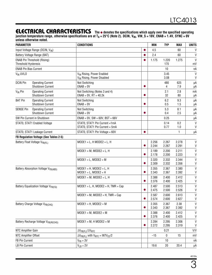
ELECTRICAL CHARACTERISTICS
PARAMETER CONDITIONS MIN TYP MAX UNITS
Input Voltage Range (DCIN, VIN) l 4.5 60 V
Battery Voltage Range (BAT) l 2.4 60 V
ENAB Pin Threshold (Rising) Threshold Hysteresis
l 1.175 1.220 170
1.275 V mV
ENAB Pin Bias Current 10 nA
VIN UVLO VIN Rising, Power Enabled VIN Rising, Power Disabled
3.45 3.08
V V
DCIN Pin Operating Current Shutdown Current
Not Switching ENAB = 0V
l
480 4
625 7.9
µA µA
VIN Pin Operating Current Shutdown Current
Not Switching (Notes 3 and 4) ENAB = 0V, RT = 40.2k
l
2.1 32
2.8 80
mA µA
BAT Pin Operating Current Shutdown Current
Not Switching ENAB = 0V
l
6.2 0.5
9.3 1.5
µA µA
SENSE Pin Operating Current Shutdown Current
Not Switching ENAB = 0V
l
5.3 0.4
8.1 2.5
µA µA
SW Pin Current in Shutdown ENAB = 0V, SW = 60V, BST = 66V 0.25 µA
STAT0, STAT1 Enabled Voltage STAT0, STAT1 Pin Current =1mA STAT0, STAT1 Pin Current = 5mA
0.14 0.77
0.2 1.0
V V
STAT0, STAT1 Leakage Current STAT0, STAT1 Pin Voltage = 60V l 1 µA
FB Regulation Voltage (See Tables 2-5)
Battery Float Voltage VFB(FL) MODE1 = L, H MODE2 = L, H
l
2.256 2.244
2.267 2.267
2.278 2.291
V V
MODE1 = M, MODE2 = L, H
l
2.189 2.178
2.200 2.200
2.211 2.223
V V
MODE1 = L, MODE2 = M
l
2.320 2.309
2.332 2.332
2.344 2.356
V V
Battery Absorption Voltage VFB(ABS) MODE1 = H, MODE2 = L, H MODE1 = L, MODE2 = H
l
2.355 2.343
2.367 2.367
2.380 2.392
V V
MODE1 = M, MODE2 = L, H
l
2.388 2.376
2.400 2.400
2.412 2.425
V V
Battery Equalization Voltage VFB(EQ) MODE1 = L, H, MODE2 = H, TMR = Cap
l
2.487 2.475
2.500 2.500
2.513 2.526
V V
MODE1 = M, MODE2 = H, TMR = Cap
l
2.587 2.574
2.600 2.600
2.613 2.627
V V
Battery Charge Voltage VFB(CHG) MODE1 = H, MODE2 = M
l
2.355 2.343
2.367 2.367
2.38 2.392
V V
MODE1 = M, MODE2 = M
l
2.388 2.376
2.400 2.400
2.412 2.425
V V
Battery Recharge Voltage VFB(RECHG) MODE1 = M, H MODE2 = M
l
2.284 2.272
2.295 2.295
2.306 2.319
V V
NTC Amplifier Gain ∆VFB(FL)/∆VNTC 0.21 V/V
NTC Amplifier Offset ∆VFB(FL) with VNTC = INTVCC/2 –15 0 15 mV
FB Pin Current VFB = 3V 10 nA
LB Pin Current VLB = 2V 19.6 20 20.4 μA
The l denotes the specifications which apply over the specified operating junction temperature range, otherwise specifications are at TA = 25°C (Note 2). DCIN, VIN, VIN_S = 18V, ENAB = 1.4V, SYNC = 0V unless otherwise noted.
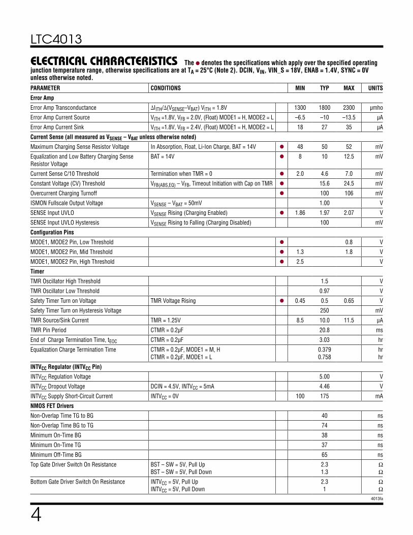
LTC4013
44013fa
PARAMETER CONDITIONS MIN TYP MAX UNITS
Error Amp
Error Amp Transconductance ∆IITH/∆(VSENSE–VBAT) VITH = 1.8V 1300 1800 2300 µmho
Error Amp Current Source VITH =1.8V, VFB = 2.0V, (Float) MODE1 = H, MODE2 = L –6.5 –10 –13.5 µA
Error Amp Current Sink VITH =1.8V, VFB = 2.4V, (Float) MODE1 = H, MODE2 = L 18 27 35 µA
Current Sense (all measured as VSENSE – VBAT unless otherwise noted)
Maximum Charging Sense Resistor Voltage In Absorption, Float, Li-Ion Charge, BAT = 14V l 48 50 52 mV
Equalization and Low Battery Charging Sense Resistor Voltage
BAT = 14V l 8 10 12.5 mV
Current Sense C/10 Threshold Termination when TMR = 0 l 2.0 4.6 7.0 mV
Constant Voltage (CV) Threshold VFB(ABS,EQ) – VFB, Timeout Initiation with Cap on TMR l 15.6 24.5 mV
Overcurrent Charging Turnoff l 100 106 mV
ISMON Fullscale Output Voltage VSENSE – VBAT = 50mV 1.00 V
SENSE Input UVLO VSENSE Rising (Charging Enabled) l 1.86 1.97 2.07 V
SENSE Input UVLO Hysteresis VSENSE Rising to Falling (Charging Disabled) 100 mV
Configuration Pins
MODE1, MODE2 Pin, Low Threshold l 0.8 V
MODE1, MODE2 Pin, Mid Threshold l 1.3 1.8 V
MODE1, MODE2 Pin, High Threshold l 2.5 V
Timer
TMR Oscillator High Threshold 1.5 V
TMR Oscillator Low Threshold 0.97 V
Safety Timer Turn on Voltage TMR Voltage Rising l 0.45 0.5 0.65 V
Safety Timer Turn on Hysteresis Voltage 250 mV
TMR Source/Sink Current TMR = 1.25V 8.5 10.0 11.5 μA
TMR Pin Period CTMR = 0.2µF 20.8 ms
End of Charge Termination Time, tEOC CTMR = 0.2µF 3.03 hr
Equalization Charge Termination Time CTMR = 0.2µF, MODE1 = M, H CTMR = 0.2µF, MODE1 = L
0.379 0.758
hr hr
INTVCC Regulator (INTVCC Pin)
INTVCC Regulation Voltage 5.00 V
INTVCC Dropout Voltage DCIN = 4.5V, INTVCC = 5mA 4.46 V
INTVCC Supply Short-Circuit Current INTVCC = 0V 100 175 mA
NMOS FET Drivers
Non-Overlap Time TG to BG 40 ns
Non-Overlap Time BG to TG 74 ns
Minimum On-Time BG 38 ns
Minimum On-Time TG 37 ns
Minimum Off-Time BG 65 ns
Top Gate Driver Switch On Resistance BST – SW = 5V, Pull Up BST – SW = 5V, Pull Down
2.3 1.3
Ω Ω
Bottom Gate Driver Switch On Resistance INTVCC = 5V, Pull Up INTVCC = 5V, Pull Down
2.3 1
Ω Ω
ELECTRICAL CHARACTERISTICS The l denotes the specifications which apply over the specified operating junction temperature range, otherwise specifications are at TA = 25°C (Note 2). DCIN, VIN, VIN_S = 18V, ENAB = 1.4V, SYNC = 0V unless otherwise noted.
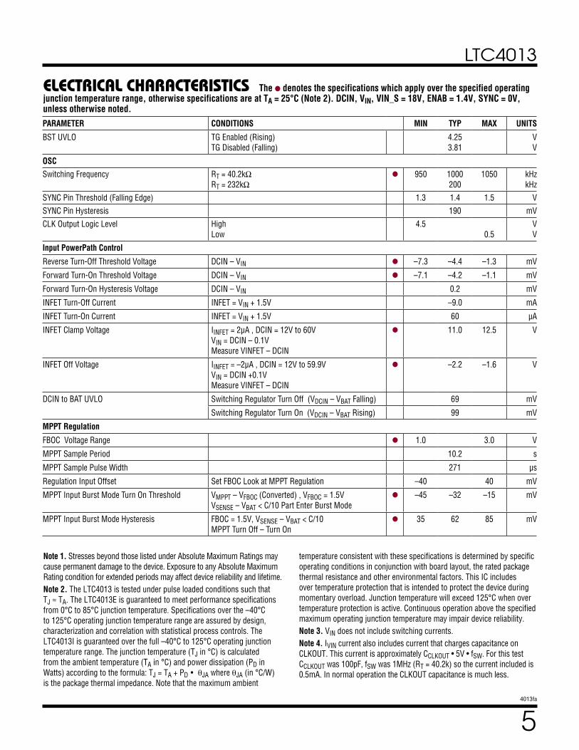
LTC4013
54013fa
ELECTRICAL CHARACTERISTICS The l denotes the specifications which apply over the specified operating junction temperature range, otherwise specifications are at TA = 25°C (Note 2). DCIN, VIN, VIN_S = 18V, ENAB = 1.4V, SYNC = 0V, unless otherwise noted.PARAMETER CONDITIONS MIN TYP MAX UNITS
BST UVLO TG Enabled (Rising) TG Disabled (Falling)
4.25 3.81
V V
OSCSwitching Frequency RT = 40.2kΩ
RT = 232kΩl 950 1000
2001050 kHz
kHzSYNC Pin Threshold (Falling Edge) 1.3 1.4 1.5 VSYNC Pin Hysteresis 190 mVCLK Output Logic Level High
Low4.5
0.5V V
Input PowerPath Control
Reverse Turn-Off Threshold Voltage DCIN – VIN l –7.3 –4.4 –1.3 mV
Forward Turn-On Threshold Voltage DCIN – VIN l –7.1 –4.2 –1.1 mV
Forward Turn-On Hysteresis Voltage DCIN – VIN 0.2 mV
INFET Turn-Off Current INFET = VIN + 1.5V –9.0 mA
INFET Turn-On Current INFET = VIN + 1.5V 60 µA
INFET Clamp Voltage IINFET = 2μA , DCIN = 12V to 60V VIN = DCIN – 0.1V Measure VINFET – DCIN
l 11.0 12.5 V
INFET Off Voltage IINFET = –2μA , DCIN = 12V to 59.9V VIN = DCIN +0.1V Measure VINFET – DCIN
l –2.2 –1.6 V
DCIN to BAT UVLO Switching Regulator Turn Off (VDCIN – VBAT Falling) 69 mV
Switching Regulator Turn On (VDCIN – VBAT Rising) 99 mV
MPPT Regulation
FBOC Voltage Range l 1.0 3.0 V
MPPT Sample Period 10.2 s
MPPT Sample Pulse Width 271 µs
Regulation Input Offset Set FBOC Look at MPPT Regulation –40 40 mV
MPPT Input Burst Mode Turn On Threshold VMPPT – VFBOC (Converted) , VFBOC = 1.5V VSENSE – VBAT < C/10 Part Enter Burst Mode
l –45 –32 –15 mV
MPPT Input Burst Mode Hysteresis FBOC = 1.5V, VSENSE – VBAT < C/10 MPPT Turn Off – Turn On
l 35 62 85 mV
Note 1. Stresses beyond those listed under Absolute Maximum Ratings may cause permanent damage to the device. Exposure to any Absolute Maximum Rating condition for extended periods may affect device reliability and lifetime. Note 2. The LTC4013 is tested under pulse loaded conditions such that TJ ≈ TA. The LTC4013E is guaranteed to meet performance specifications from 0°C to 85°C junction temperature. Specifications over the –40°C to 125°C operating junction temperature range are assured by design, characterization and correlation with statistical process controls. The LTC4013I is guaranteed over the full –40°C to 125°C operating junction temperature range. The junction temperature (TJ in °C) is calculated from the ambient temperature (TA in °C) and power dissipation (PD in Watts) according to the formula: TJ = TA + PD • θJA where θJA (in °C/W) is the package thermal impedance. Note that the maximum ambient
temperature consistent with these specifications is determined by specific operating conditions in conjunction with board layout, the rated package thermal resistance and other environmental factors. This IC includes over temperature protection that is intended to protect the device during momentary overload. Junction temperature will exceed 125°C when over temperature protection is active. Continuous operation above the specified maximum operating junction temperature may impair device reliability.Note 3. VIN does not include switching currents. Note 4. IVIN current also includes current that charges capacitance on CLKOUT. This current is approximately CCLKOUT • 5V • fSW. For this test CCLKOUT was 100pF, fSW was 1MHz (RT = 40.2k) so the current included is 0.5mA. In normal operation the CLKOUT capacitance is much less.
LTC4013
64013fa
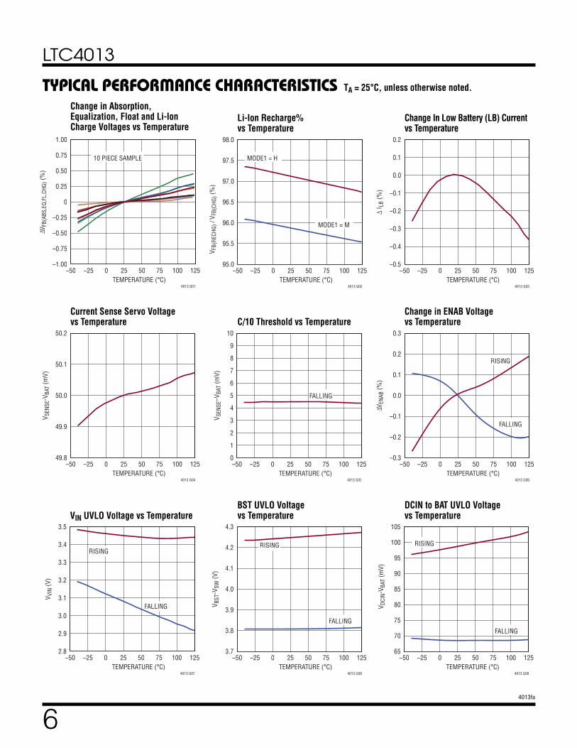
TYPICAL PERFORMANCE CHARACTERISTICS
Current Sense Servo Voltage vs Temperature C/10 Threshold vs Temperature
Change in ENAB Voltage vs Temperature
VIN UVLO Voltage vs TemperatureBST UVLO Voltage vs Temperature
DCIN to BAT UVLO Voltage vs Temperature
Change in Absorption, Equalization, Float and Li-Ion Charge Voltages vs Temperature
Li-Ion Recharge% vs Temperature
Change In Low Battery (LB) Current vs Temperature
TA = 25°C, unless otherwise noted.
10 PIECE SAMPLE
TEMPERATURE (°C)–50 –25 0 25 50 75 100 125
–1.00
–0.75
–0.50
–0.25
0
0.25
0.50
0.75
1.00
∆VFB
(ABS
,EQ,
FL,C
HG) (
%)
4013 G01
MODE1 = H
MODE1 = M
TEMPERATURE (°C)–50 –25 0 25 50 75 100 125
95.0
95.5
96.0
96.5
97.0
97.5
98.0
V FB(
CHG)
(%)
V FB(
RECH
G) /
4013 G02TEMPERATURE (°C)
–50 –25 0 25 50 75 100 125–0.5
–0.4
–0.3
–0.2
–0.1
0.0
0.1
0.2
∆ I L
B (%
)
4013 G03
TEMPERATURE (°C)–50 –25 0 25 50 75 100 125
49.8
49.9
50.0
50.1
50.2
V SEN
SE-V
BAT
(mV)
4013 G04
FALLING
TEMPERATURE (°C)–50 –25 0 25 50 75 100 125
0
1
2
3
4
5
6
7
8
9
10
V SEN
SE–V
BAT
(mV)
4013 G05
RISING
FALLING
TEMPERATURE (°C)–50 –25 0 25 50 75 100 125
–0.3
–0.2
–0.1
0.0
0.1
0.2
0.3
∆VEN
AB (%
)
4013 G06
RISING
FALLING
TEMPERATURE (°C)–50 –25 0 25 50 75 100 125
2.8
2.9
3.0
3.1
3.2
3.3
3.4
3.5
V VIN
(V)
4013 G07
RISING
FALLING
TEMPERATURE (°C)–50 –25 0 25 50 75 100 125
3.7
3.8
3.9
4.0
4.1
4.2
4.3
V BST
-VSW
(V)
4013 G08
RISING
FALLING
TEMPERATURE (°C)–50 –25 0 25 50 75 100 125
65
70
75
80
85
90
95
100
105
V DCI
N-V B
AT (m
V)
4013 G09
LTC4013
74013fa
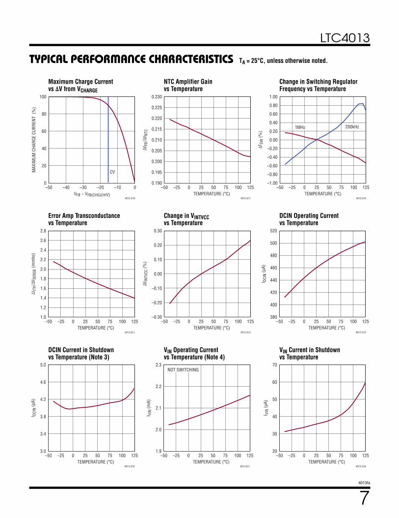
TYPICAL PERFORMANCE CHARACTERISTICS
Maximum Charge Current vs ΔV from VCHARGE
Error Amp Transconductance vs Temperature
DCIN Current in Shutdown vs Temperature (Note 3)
NTC Amplifier Gain vs Temperature
Change in VINTVCC vs Temperature
VIN Operating Current vs Temperature (Note 4)
Change in Switching Regulator Frequency vs Temperature
DCIN Operating Current vs Temperature
VIN Current in Shutdown vs Temperature
TA = 25°C, unless otherwise noted.
CV
VFB – VFB(CHG)(mV)
–50 –40 –30 –20 –10 00
20
40
60
80
100
MAX
IMUM
CHA
RGE
CURR
ENT
(%)
4013 G10TEMPERATURE (°C)
–50 –25 0 25 50 75 100 1250.190
0.195
0.200
0.205
0.210
0.215
0.220
0.225
0.230
∆VFB
/∆V N
TC
4013 G11
1MHz 200kHz
TEMPERATURE (°C)–50 –25 0 25 50 75 100 125
–1.00
–0.80
–0.60
–0.40
–0.20
0.00
0.20
0.40
0.60
0.80
1.00
∆FSW
(%)
4013 G12
TEMPERATURE (°C)–50 –25 0 25 50 75 100 125
1.0
1.2
1.4
1.6
1.8
2.0
2.2
2.4
2.6
2.8
∆IIT
H/∆V
SENS
E (m
mho
)
4013 G13TEMPERATURE (°C)
–50 –25 0 25 50 75 100 125–0.30
–0.20
–0.10
0.00
0.10
0.20
0.30
∆VIN
TVCC
(%)
4013 G14TEMPERATURE (°C)
–50 –25 0 25 50 75 100 125380
400
420
440
460
480
500
520
I DCI
N (µ
A)
4013 G15
TEMPERATURE (°C)–50 –25 0 25 50 75 100 125
3.0
3.4
3.8
4.2
4.6
5.0
I DCI
N (µ
A)
4013 G16
NOT SWITCHING
TEMPERATURE (°C)–50 –25 0 25 50 75 100 125
1.9
2.0
2.1
2.2
2.3
I VIN
(mA)
4013 G17TEMPERATURE (°C)
–50 –25 0 25 50 75 100 12520
30
40
50
60
70
I VIN
(µA)
4013 G18
LTC4013
84013fa
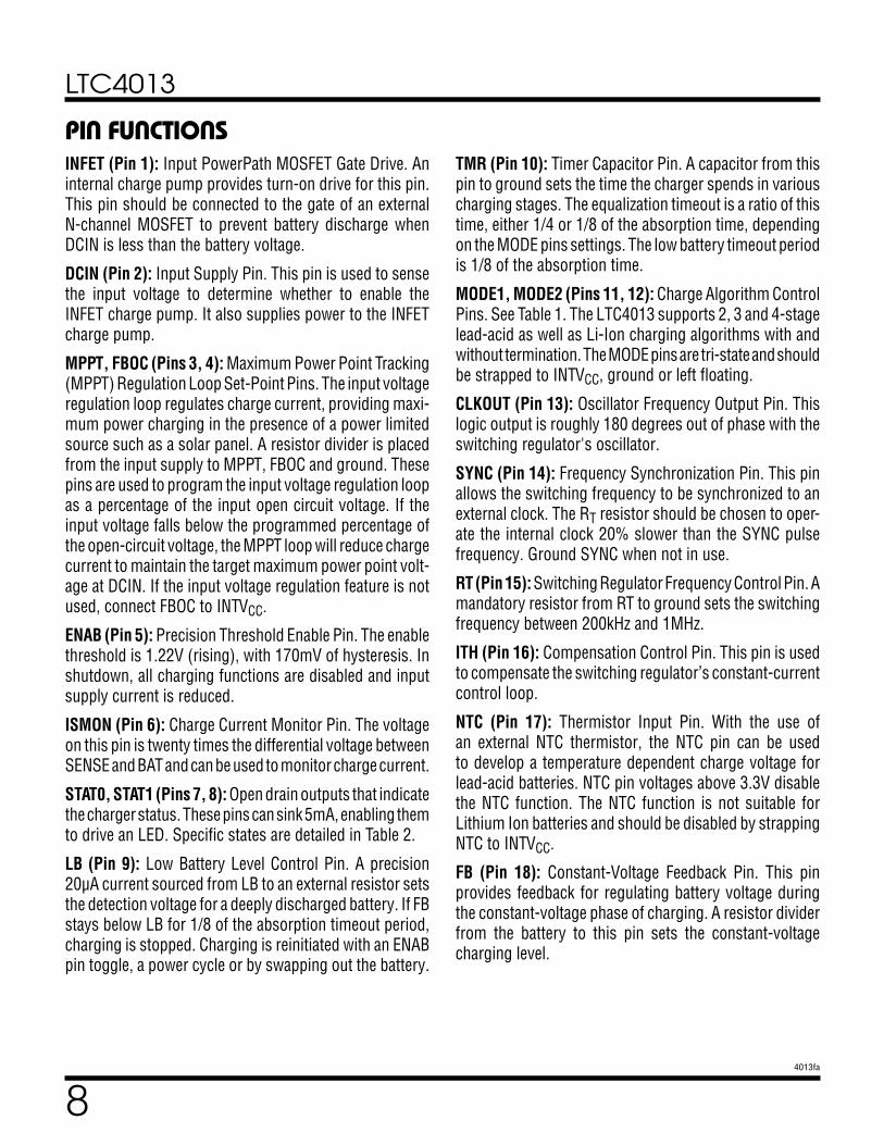
PIN FUNCTIONSINFET (Pin 1): Input PowerPath MOSFET Gate Drive. An internal charge pump provides turn-on drive for this pin. This pin should be connected to the gate of an external N-channel MOSFET to prevent battery discharge when DCIN is less than the battery voltage.
DCIN (Pin 2): Input Supply Pin. This pin is used to sense the input voltage to determine whether to enable the INFET charge pump. It also supplies power to the INFET charge pump.
MPPT, FBOC (Pins 3, 4): Maximum Power Point Tracking (MPPT) Regulation Loop Set-Point Pins. The input voltage regulation loop regulates charge current, providing maxi-mum power charging in the presence of a power limited source such as a solar panel. A resistor divider is placed from the input supply to MPPT, FBOC and ground. These pins are used to program the input voltage regulation loop as a percentage of the input open circuit voltage. If the input voltage falls below the programmed percentage of the open-circuit voltage, the MPPT loop will reduce charge current to maintain the target maximum power point volt-age at DCIN. If the input voltage regulation feature is not used, connect FBOC to INTVCC.
ENAB (Pin 5): Precision Threshold Enable Pin. The enable threshold is 1.22V (rising), with 170mV of hysteresis. In shutdown, all charging functions are disabled and input supply current is reduced.
ISMON (Pin 6): Charge Current Monitor Pin. The voltage on this pin is twenty times the differential voltage between SENSE and BAT and can be used to monitor charge current.
STAT0, STAT1 (Pins 7, 8): Open drain outputs that indicate the charger status. These pins can sink 5mA, enabling them to drive an LED. Specific states are detailed in Table 2.
LB (Pin 9): Low Battery Level Control Pin. A precision 20µA current sourced from LB to an external resistor sets the detection voltage for a deeply discharged battery. If FB stays below LB for 1/8 of the absorption timeout period, charging is stopped. Charging is reinitiated with an ENAB pin toggle, a power cycle or by swapping out the battery.
TMR (Pin 10): Timer Capacitor Pin. A capacitor from this pin to ground sets the time the charger spends in various charging stages. The equalization timeout is a ratio of this time, either 1/4 or 1/8 of the absorption time, depending on the MODE pins settings. The low battery timeout period is 1/8 of the absorption time.
MODE1, MODE2 (Pins 11, 12): Charge Algorithm Control Pins. See Table 1. The LTC4013 supports 2, 3 and 4-stage lead-acid as well as Li-Ion charging algorithms with and without termination. The MODE pins are tri-state and should be strapped to INTVCC, ground or left floating.
CLKOUT (Pin 13): Oscillator Frequency Output Pin. This logic output is roughly 180 degrees out of phase with the switching regulator's oscillator.
SYNC (Pin 14): Frequency Synchronization Pin. This pin allows the switching frequency to be synchronized to an external clock. The RT resistor should be chosen to oper-ate the internal clock 20% slower than the SYNC pulse frequency. Ground SYNC when not in use.
RT (Pin 15): Switching Regulator Frequency Control Pin. A mandatory resistor from RT to ground sets the switching frequency between 200kHz and 1MHz.
ITH (Pin 16): Compensation Control Pin. This pin is used to compensate the switching regulator’s constant-current control loop.
NTC (Pin 17): Thermistor Input Pin. With the use of an external NTC thermistor, the NTC pin can be used to develop a temperature dependent charge voltage for lead-acid batteries. NTC pin voltages above 3.3V disable the NTC function. The NTC function is not suitable for Lithium Ion batteries and should be disabled by strapping NTC to INTVCC.
FB (Pin 18): Constant-Voltage Feedback Pin. This pin provides feedback for regulating battery voltage during the constant-voltage phase of charging. A resistor divider from the battery to this pin sets the constant-voltage charging level.
LTC4013
94013fa
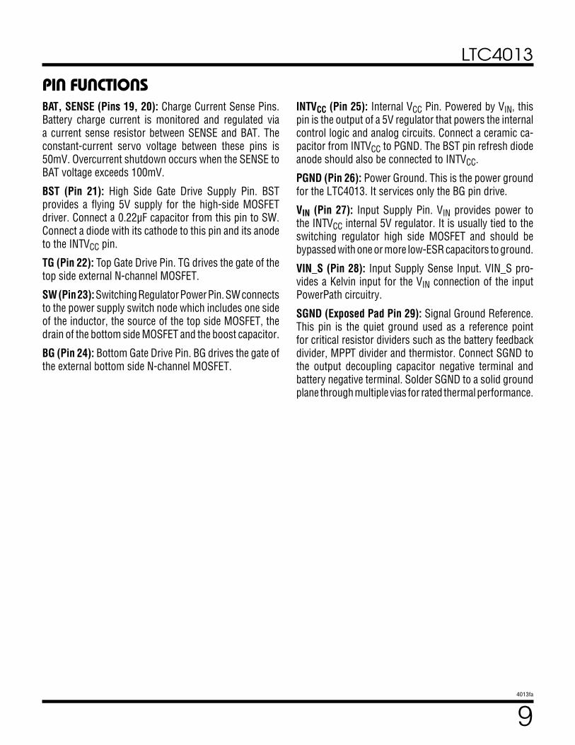
PIN FUNCTIONSBAT, SENSE (Pins 19, 20): Charge Current Sense Pins. Battery charge current is monitored and regulated via a current sense resistor between SENSE and BAT. The constant-current servo voltage between these pins is 50mV. Overcurrent shutdown occurs when the SENSE to BAT voltage exceeds 100mV.
BST (Pin 21): High Side Gate Drive Supply Pin. BST provides a flying 5V supply for the high-side MOSFET driver. Connect a 0.22µF capacitor from this pin to SW. Connect a diode with its cathode to this pin and its anode to the INTVCC pin.
TG (Pin 22): Top Gate Drive Pin. TG drives the gate of the top side external N-channel MOSFET.
SW (Pin 23): Switching Regulator Power Pin. SW connects to the power supply switch node which includes one side of the inductor, the source of the top side MOSFET, the drain of the bottom side MOSFET and the boost capacitor.
BG (Pin 24): Bottom Gate Drive Pin. BG drives the gate of the external bottom side N-channel MOSFET.
INTVCC (Pin 25): Internal VCC Pin. Powered by VIN, this pin is the output of a 5V regulator that powers the internal control logic and analog circuits. Connect a ceramic ca-pacitor from INTVCC to PGND. The BST pin refresh diode anode should also be connected to INTVCC.
PGND (Pin 26): Power Ground. This is the power ground for the LTC4013. It services only the BG pin drive.
VIN (Pin 27): Input Supply Pin. VIN provides power to the INTVCC internal 5V regulator. It is usually tied to the switching regulator high side MOSFET and should be bypassed with one or more low-ESR capacitors to ground.
VIN_S (Pin 28): Input Supply Sense Input. VIN_S pro-vides a Kelvin input for the VIN connection of the input PowerPath circuitry.
SGND (Exposed Pad Pin 29): Signal Ground Reference. This pin is the quiet ground used as a reference point for critical resistor dividers such as the battery feedback divider, MPPT divider and thermistor. Connect SGND to the output decoupling capacitor negative terminal and battery negative terminal. Solder SGND to a solid ground plane through multiple vias for rated thermal performance.
LTC4013
104013fa
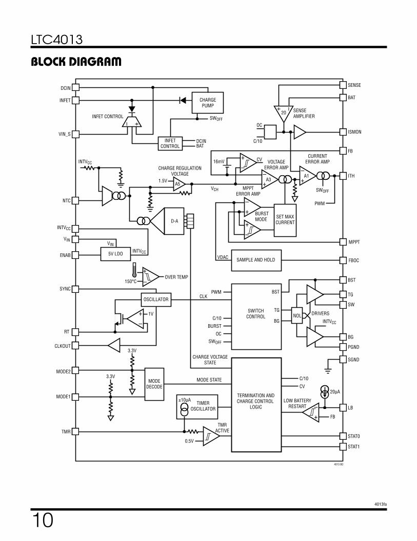
BLOCK DIAGRAM
– +
DCINSENSE
ISMON
FB
ITH
MPPT
ENAB
SYNC
RT
NTC
CHARGE REGULATIONVOLTAGE
1.5V
MODE2
MODEDECODE
TMRACTIVE
CLKOUT
1V
FBOC
D-A
BST
TG
BG
SGND
PGND
STAT0
LB
±10µA
MODE STATE
STAT1
4013 BD
SW
CURRENTERROR AMP
SENSE AMPLIFIER
BATINFET
INFET CONTROL SWOFF
SWOFF
SWOFF
OC
C/10
C/10
CV
CLK
CHARGE VOLTAGESTATE
BURST
BST
TG
BG
PWM
DCIN
OC
C/10BAT
VIN_S
VINVIN
TIMEROSCILLATOR
–+
–+
INTVCC
INTVCC
INTVCC
INTVCC
MODE1
TMR
INFETCONTROL
CHARGEPUMP
LOW BATTERYRESTART
DRIVERS
FB
0.5V
20µA
–+
3.3V
3.3V
–+
OVER TEMP150°C
A5
5V LDO
OSCILLATOR
20
16mV
VCH
PWM
BURST MODE
MPPTERROR AMP
VDAC
SET MAXCURRENT
CV–+
–+
VOLTAGEERROR AMP–+
A3
–+
–+
A1
SAMPLE AND HOLD
SWITCHCONTROL
TERMINATION ANDCHARGE CONTROL
LOGIC
NOL
LTC4013
114013fa
OPERATIONOVERVIEW
The LTC4013 is a high-voltage multi-chemistry battery charger with specific focus on lead-acid batteries. It incorporates a step-down (buck) DC/DC synchronous switching controller using external N-channel MOSFETS for high efficiency. It accommodates a wide range of bat-tery voltages from 2.4V to 60V and is optimized for high current charging applications.
Selectable charger profiles are:
2-stage charging: constant-current (bulk) to constant-voltage with and without timer termination.
3-stage lead-acid charging: bulk, absorption and float with low battery restart and either charge-current (C/10) or safety-timer absorption to float transition control.
4-stage lead-acid charging: bulk, absorption, equaliza-tion, and float with low battery restart and safety-timer equalization cutoff and safety-timer absorption to float transition control.
Li-Ion constant-current to constant-voltage charging with either charge-current (C/10) or safety-timer charge termination.
DC/DC OPERATION
(See Block Diagram)
The LTC4013 uses a fixed-frequency, average current mode DC/DC converter to regulate charge current. When the battery reaches the charge voltage, current is reduced by a voltage regulation loop.
Battery current is sensed via a resistor placed between SENSE and BAT. The amplified signal is compared to a voltage that represents the maximum allowable charge current and regulates the average current by controlling the duty cycle of the output switches. The current con-trol loop servos the differential voltage between SENSE and BAT to 50mV making ICHGMAX = 50mV/RSENSE. A frequency-compensation pin (ITH) is used to control the constant-current feedback loop stability.
At startup, the maximum current is ramped over approxi-mately 1.6ms to provide soft start. There is an additional burst mode feature used for maximum power point transfer to facilitate low solar panel current operation.
When the battery voltage reaches the programmed charge voltage, error amplifier A3 adjusts the charge current to servo the battery voltage to the programmed level and can reduce the current to zero.
The charge voltage is determined by amplifier A5 and the charge algorithm selected. The voltage can follow a continuous function of temperature controlled by an am-plifier connected to the NTC pin. A resistor divider with a thermistor sets the temperature coefficient of the voltage.
The switching regulator's oscillator frequency is set by a resistor from the RT pin to ground. The clock frequency can optionally be synchronized to an external oscillator by using the SYNC pin.
The step-down (buck) switching regulator uses external low RDS(ON) MOSFETs for both high and low side switches to deliver high charge current. When the current level falls below ICHGMAX/10 the bottom MOSFET is disabled and switching operation is discontinuous with only the bottom side MOSFET body diode used for low side conduction. This diode emulation mode ensures the battery is not discharged by continuous conduction.
Supply voltage for the top gate drive is generated by a boost circuit that uses an external diode and boost capacitor charged from INTVCC. If BST - SW is below 3.8V (e.g. at startup), the bottom side MOSFET is enabled to refresh the BST capacitor.
Solar Panel Maximum Power Point Tracking
If the MPPT function is enabled (FBOC pin voltage < 3V), the LTC4013 employs an MPPT circuit that compares a stored open-circuit input voltage measurement against the instantaneous DCIN voltage while charging. The LTC4013 then uses an input voltage sense amplifier to reduce the charge current if the DCIN voltage falls below the user
LTC4013
124013fa
defined percentage of the open-circuit voltage. With this algorithm the LTC4013 optimizes power transfer for a variety of different input sources.
When MPPT is enabled, the LTC4013 periodically measures the open-circuit input voltage. About once every 10.2s the LTC4013 pauses charging, samples the input voltage as measured through a resistor divider at the FBOC pin, and reproduces this value internally with a digital-to-analog converter (DAC). When charging resumes, the DAC volt-age, VDAC, is compared against the MPPT pin voltage that is programmed with a resistor divider. If the MPPT voltage falls below VDAC, charge current is reduced to regulate the input voltage at that level. This regulation loop maintains the input voltage at or above a user defined level that corresponds to the peak power available from the applied source. Regular input sampling is useful, for instance, to provide first order temperature compensation of a solar panel.
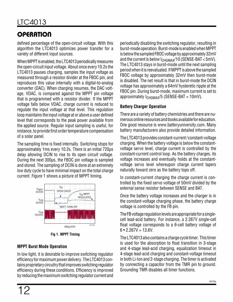
The sampling time is fixed internally. Switching stops for approximately 1ms every 10.2s. There is an initial 720µs delay allowing DCIN to rise to its open circuit voltage. During the next 300µs, the FBOC pin voltage is sampled and stored. The sampling of DCIN is done at an extremely low duty cycle to have minimal impact on the total charge current. Figure 1 shows a picture of MPPT timing.
OPERATIONperiodically disabling the switching regulator, resulting in burst-mode operation. Burst-mode is enabled when MPPT is below the sampled FBOC voltage by approximately 32mV and the current is below ICHGMAX/10 (SENSE-BAT < 5mV). The LTC4013 stays in burst-mode until the next sampling period when it is reevaluated. If MPPT is above the sampled FBOC voltage by approximately 32mV then burst-mode is disabled. The net result is that in burst-mode the DCIN voltage has approximately a 64mV hysteretic ripple at the FBOC pin. During burst-mode, maximum current is set to approximately ICHGMAX/5 (SENSE-BAT = 10mV).
Battery Charger Operation
There are a variety of battery chemistries and there are nu-merous online resources and books available for education. One good resource is www.batteryuniversity.com. Many battery manufacturers also provide detailed information.
The LTC4013 provides constant-current / constant-voltage charging. When the battery voltage is below the constant-voltage servo level, charge current is controlled by the constant-current control loop. As the battery charges, its voltage increases and eventually holds at the constant-voltage servo level whereupon charge current tapers naturally toward zero as the battery tops off.
In constant-current charging the charge current is con-trolled by the fixed servo voltage of 50mV divided by the external sense resistor between SENSE and BAT.
Once the battery voltage increases and the charger is in the constant-voltage charging phase, the battery charge voltage is controlled by the FB pin.
The FB voltage regulation levels are appropriate for a single-cell lead-acid battery. For instance, a 2.267V single-cell float voltage corresponds to a 6-cell battery voltage of 6 • 2.267V = 13.6V.
The LTC4013 also contains a charge cycle timer. This timer is used for the absorption to float transition in 3-stage and 4-stage lead-acid charging, equalization timeout in 4-stage lead-acid charging and constant-voltage timeout in both Li-Ion and 2-stage charging. The timer is activated by connecting a capacitor from the TMR pin to ground. Grounding TMR disables all timer functions.
Fig 1. MPPT Timing
VIN
OPEN CIRUIT
INFET TURN OFF
VIN MPPTREGULATED
400µs/DIV
VSW10V/DIV
VINFET5V/DIV
VVIN5V/DIV
4013 F01
MPPT Burst Mode Operation
In low light, it is desirable to improve switching regulator efficiency for maximum power delivery. The LTC4013 con-tains proprietary circuitry that improves switching regulator efficiency during these conditions. Efficiency is improved by reducing the maximum switching regulator current and
LTC4013
134013fa
OPERATIONbattery fault is indicated by STAT0 turning off and STAT1 turning on.
There are two voltage settings available for 2-stage charg-ing as noted in Table 1.
2-stage charging for a lead-acid battery has the disad-vantage of not fully charging the battery, resulting in diminished capacity over time due to increased deposits on the electrodes.
3-Stage Charging
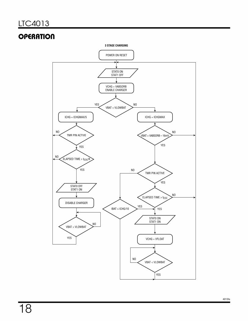
A more complete lead-acid battery charging method is 3-stage charging utilizing an absorption phase which increases the amount of stored charge in the battery. Because the absorption voltage is above the electro-chemical float level, the time that the battery stays in this condition should be limited either by a timer (the safest method) or waiting for the charge current to diminish. Minor gassing of water from the battery can occur from charging the battery above the float voltage, so choosing an appropriate absorption voltage is important for best battery life. Always consult the battery manufacturer for their recommendations.
3-stage charging is initiated on input power-up whereupon the battery charges with constant-current at ICHGMAX toward VFB(ABS). The STAT0 pin pulls low immediately indicating that charging has begun. As the battery voltage approaches VFB(ABS), charge current naturally tapers to zero. When the charge current drops to ICHGMAX/10, STAT1 also pulls low and the charge voltage setting changes to the VFB(FL) voltage. At this lower level, the constant-voltage control loop will "capture" and hold the battery voltage as it slowly drops from VFB(ABS) down to VFB(FL).
Alternately, the transition from absorption charging to float charging can be controlled with the timer by placing a capacitor on the TMR pin. When the battery voltage reaches constant-voltage in the absorption phase, the timer begins. At the end of the accumulated timer period in constant-voltage mode at VFB(ABS), the charge voltage changes to the VFB(FL) voltage and will remain there. Again, STAT1 turns on, indicating the transition from the VFB(ABS) charging level to the VFB(FL) charging level.
The LB pin provides a user adjustable low battery voltage setting that sets the re-start level in 2-stage, 3-stage and 4-stage charging and the low battery fault level in Li-Ion charging. The LB pin produces a precision 20µA current which results in a precision voltage when a resistor is placed from LB to ground. The LB pin is compared internally to the FB pin for low battery determination.
Four possible charging algorithms can be selected by pin strapping or manipulating the MODE0 and MODE1 pins (see Table 1). These pins should be tied either low (GND), high (INTVCC) or mid (floating). The charge algorithms are described below.
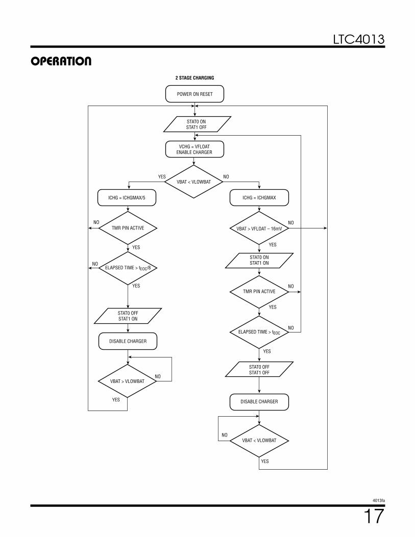
2-Stage Charging
2-stage charging is useful for batteries with no absorption preconditioning. Charging is initiated on input power-up whereupon the battery charges with constant-current at ICHGMAX toward VFB(FL). The STAT0 pin pulls low im-mediately indicating that charging has begun. Once the battery terminals approach VFB(FL), the constant-voltage control loop takes over holding the battery voltage steady as the charge current naturally tapers to zero. Once the constant-voltage loop takes control, the STAT1 pin also pulls low indicating the change from constant-current to constant-voltage charging.
If a capacitor is used on the TMR pin, the charge cycle terminates after an accumulated period of tEOC in constant-voltage mode at which time STAT0 and STAT1 will indicate termination by switching off. Alternately, if the TMR pin is grounded, 2-stage charging will charge forever at VFB(FL) with no termination.
Charging is re-initiated from termination if the FB-referred battery voltage drops below the LB threshold voltage as set by the LB pin, or if the LTC4013 is powered off and back on by cycling the ENAB pin or input power.
Defective battery protection is enabled if the timer capaci-tor is used. Whenever the FB-referred battery voltage is below the LB threshold, charge current is automatically reduced to ICHGMAX/5. If a defective battery remains below the low battery threshold longer than 1/8 of the timer period (tEOC/8) the charge cycle terminates. A defective
LTC4013
144013fa
OPERATIONIf a load subsequently pulls the FB-referred battery voltage below the LB pin, or if the LTC4013 is powered off and back on by cycling the ENAB pin or input power, a new 3-stage charge cycle is initiated with a new absorption phase.
Defective battery protection is enabled if the timer capaci-tor is used. Whenever the FB-referred battery voltage is below the LB threshold, charge current is automatically reduced to ICHGMAX/5. If a defective battery remains below the low battery threshold longer than 1/8 of the timer period (tEOC/8) the charge cycle terminates. A defective battery fault is indicated by STAT0 turning off and STAT1 turning on.
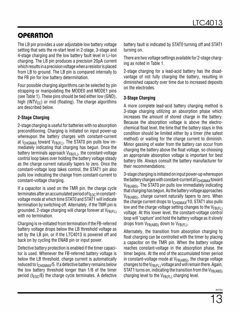
There are different options for absorption and float voltages. Table 1 details the MODE pins settings and FB voltages. Figure 2 shows an example of a 3-stage charge cycle.
ICHGMAXVABSORPTION
VFLOATCURRENT
VOLTAGE
4013 F02
1 2 3
BULK ABSORPTION FLOAT
Figure 2. 3-Stage Charge Cycle
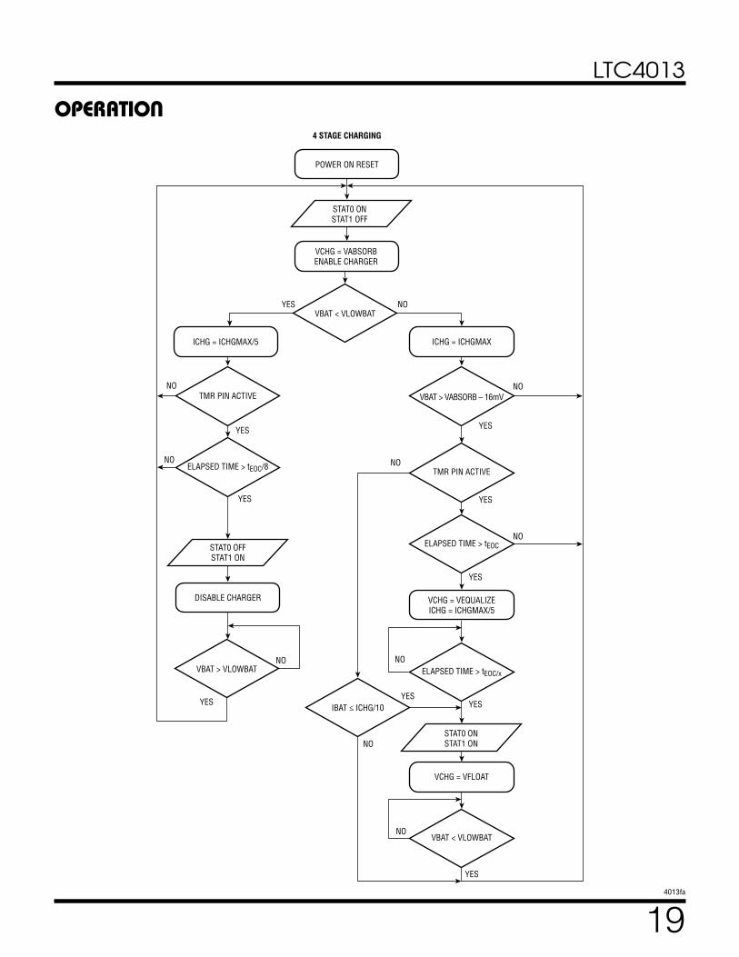
4-Stage Charging
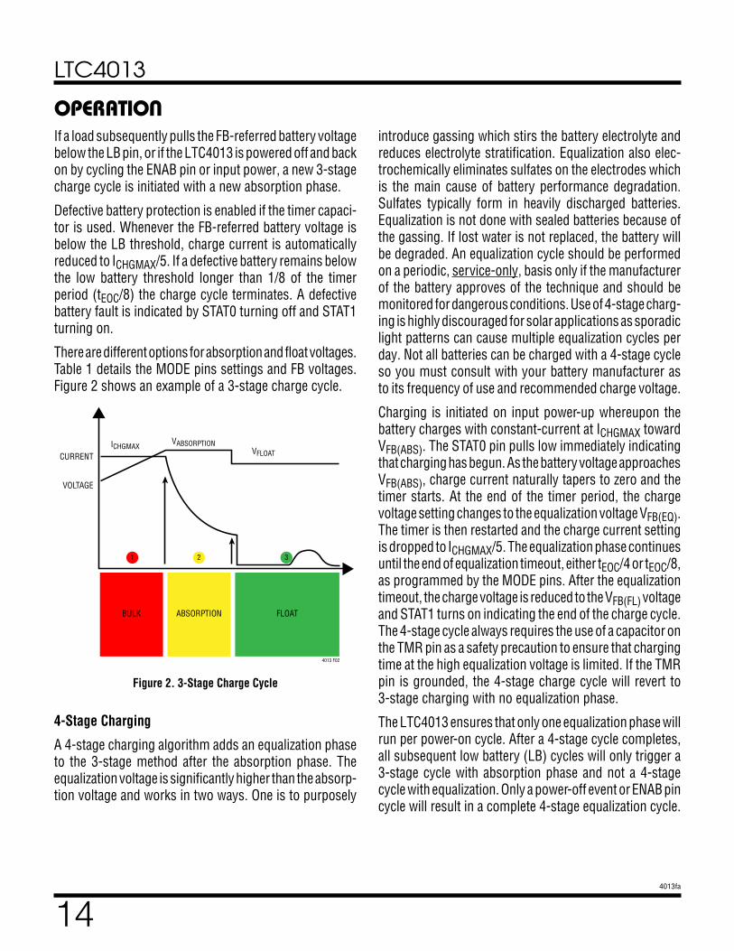
A 4-stage charging algorithm adds an equalization phase to the 3-stage method after the absorption phase. The equalization voltage is significantly higher than the absorp-tion voltage and works in two ways. One is to purposely
introduce gassing which stirs the battery electrolyte and reduces electrolyte stratification. Equalization also elec-trochemically eliminates sulfates on the electrodes which is the main cause of battery performance degradation. Sulfates typically form in heavily discharged batteries. Equalization is not done with sealed batteries because of the gassing. If lost water is not replaced, the battery will be degraded. An equalization cycle should be performed on a periodic, service-only, basis only if the manufacturer of the battery approves of the technique and should be monitored for dangerous conditions. Use of 4-stage charg-ing is highly discouraged for solar applications as sporadic light patterns can cause multiple equalization cycles per day. Not all batteries can be charged with a 4-stage cycle so you must consult with your battery manufacturer as to its frequency of use and recommended charge voltage.
Charging is initiated on input power-up whereupon the battery charges with constant-current at ICHGMAX toward VFB(ABS). The STAT0 pin pulls low immediately indicating that charging has begun. As the battery voltage approaches VFB(ABS), charge current naturally tapers to zero and the timer starts. At the end of the timer period, the charge voltage setting changes to the equalization voltage VFB(EQ). The timer is then restarted and the charge current setting is dropped to ICHGMAX/5. The equalization phase continues until the end of equalization timeout, either tEOC/4 or tEOC/8, as programmed by the MODE pins. After the equalization timeout, the charge voltage is reduced to the VFB(FL) voltage and STAT1 turns on indicating the end of the charge cycle. The 4-stage cycle always requires the use of a capacitor on the TMR pin as a safety precaution to ensure that charging time at the high equalization voltage is limited. If the TMR pin is grounded, the 4-stage charge cycle will revert to 3-stage charging with no equalization phase.
The LTC4013 ensures that only one equalization phase will run per power-on cycle. After a 4-stage cycle completes, all subsequent low battery (LB) cycles will only trigger a 3-stage cycle with absorption phase and not a 4-stage cycle with equalization. Only a power-off event or ENAB pin cycle will result in a complete 4-stage equalization cycle.
LTC4013
154013fa
OPERATION
ICHGMAXVABSORPTION
VEQUALIZATION
VFLOATCURRENT
VOLTAGE
4013 F02
1 2 3 4
BULK ABSORPTION FLOAT
EQUA
LIZA
TION
Figure 3. 4-Stage Charge Cycle
Defective battery protection is enabled if the timer capaci-tor is used. Whenever the FB-referred battery voltage is below the LB threshold, charge current is automatically reduced to ICHGMAX/5. If a defective battery remains below the low battery threshold longer than 1/8 of the timer period (tEOC/8) the charge cycle terminates. A defective battery fault is indicated by STAT0 turning off and STAT1 turning on.
Figure 3 shows an example of a 4-stage charge cycle.
Once the timer expires (tEOC), charging is terminated. Al-ternately, if the TMR pin is grounded, the timer is disabled and charging terminates when the charge current drops to 1/10 of ICHGMAX (C/10). Termination is indicated by STAT0 and STAT1 turning off.
The LTC4013 will begin charging again if the FB-referred battery voltage falls below the LiIon recharge level VFB(RECHG). The recharge voltage is either 97.0% or 95.6% of VFB(CHG) depending on the MODE pins. To avoid frequent recharge events due to voltage sag on LiFePO4 batteries, the wider difference is recommended.
Defective battery protection is enabled if the timer capaci-tor is used. Whenever the FB-referred battery voltage is below the LB threshold, charge current is automatically reduced to ICHGMAX/5. If a defective battery remains below the low battery threshold longer than 1/8 of the timer period (tEOC/8) the charge cycle terminates. A defective battery fault is indicated by STAT0 turning off and STAT1 turning on.
Mode Pins and Battery Charge Voltages
The LTC4013 provides several different options for setting the VFB(FL), VFB(ABS) and VFB(EQ) voltages. In normal mode, single-cell absorption is approximately 100mV above float (600mV for 6 cells), equalization is then approximately 133mV above absorption (800mV for 6 cells). Another option uses a wider voltage spread where single-cell ab-sorption voltage is 200mV above float (1.2V for 6 cells) and equalization is 200mV above absorption (1.2V for 6 cells). Absolute voltages are adjusted through the FB resistor divider to gain these voltages up proportionately. It is important to consult your battery manufacturer for their suggestion on charging voltages. There is no industry consensus and it depends heavily on the type of battery and anticipated usage.
Table 1 shows the MODE0/1 pin settings to select the charge algorithm and the range of charge voltage set-tings for the normal and wide spread voltage modes and Table 2 shows the STAT0/1 indicator pin values in various charging states.
Li-Ion Charging
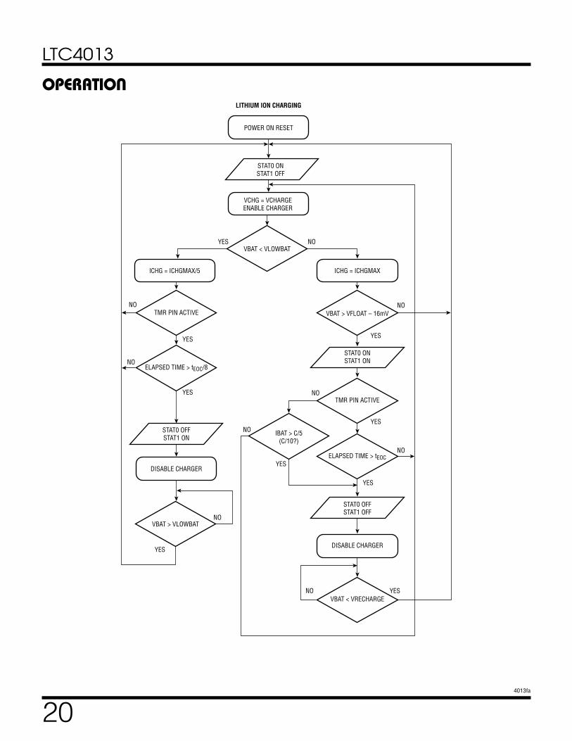
The LTC4013 can also charge Li-Ion batteries including Li-Polymer and LiFePO4.
Charging is initiated on input power-up whereupon the battery charges with constant-current at ICHGMAX toward VFB(CHG). The STAT0 pin pulls low immediately indicating that charging has begun. As the battery voltage approaches VFB(CHG), charge current naturally tapers to zero. The STAT1 pin also turns on indicating constant-voltage operation. There are two options for Li-Ion charge termination. If a capacitor is included on the TMR pin, the timer starts when the battery reaches the constant-voltage regulation point.
LTC4013
164013fa
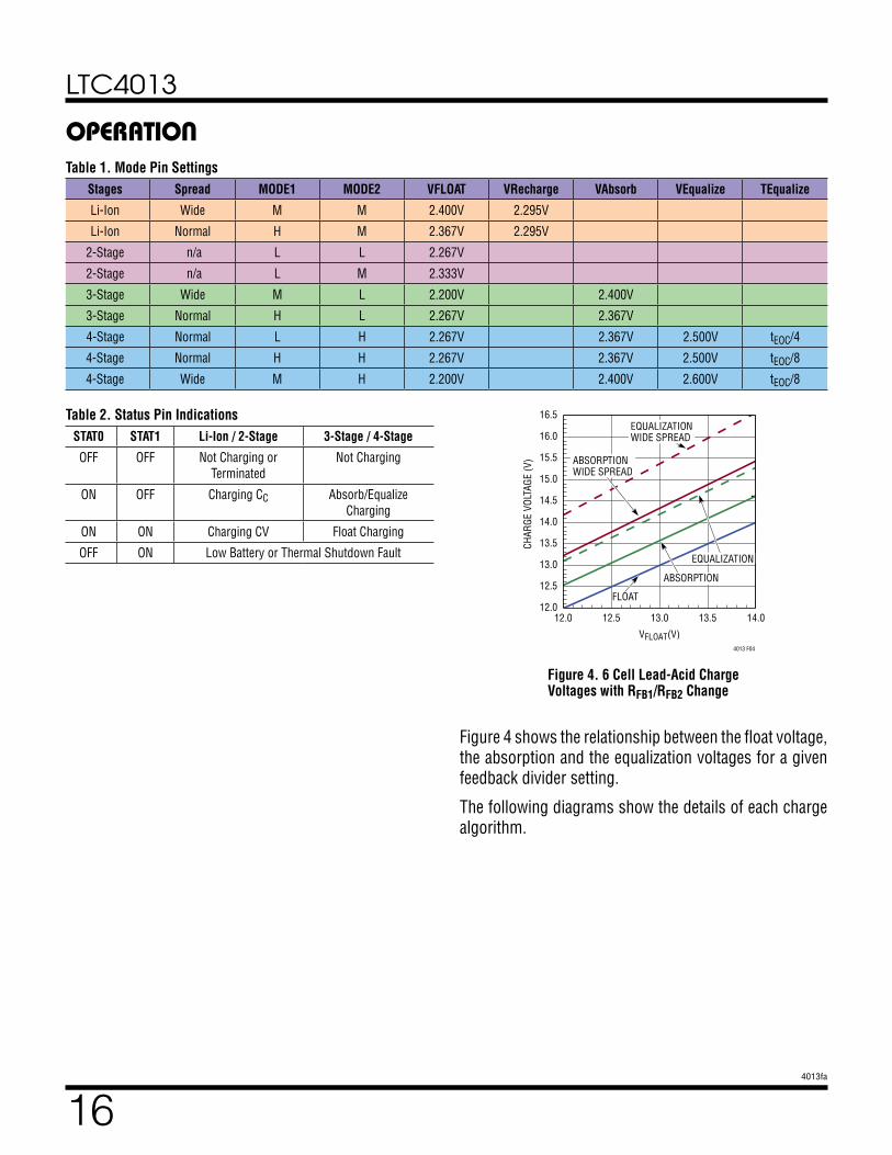
Figure 4 shows the relationship between the float voltage, the absorption and the equalization voltages for a given feedback divider setting.
The following diagrams show the details of each charge algorithm.
OPERATION
Table 2. Status Pin IndicationsSTAT0 STAT1 Li-Ion / 2-Stage 3-Stage / 4-Stage
OFF OFF Not Charging or Terminated
Not Charging
ON OFF Charging CC Absorb/Equalize Charging
ON ON Charging CV Float Charging
OFF ON Low Battery or Thermal Shutdown Fault
Table 1. Mode Pin SettingsStages Spread MODE1 MODE2 VFLOAT VRecharge VAbsorb VEqualize TEqualize
Li-Ion Wide M M 2.400V 2.295V
Li-Ion Normal H M 2.367V 2.295V
2-Stage n/a L L 2.267V
2-Stage n/a L M 2.333V
3-Stage Wide M L 2.200V 2.400V
3-Stage Normal H L 2.267V 2.367V
4-Stage Normal L H 2.267V 2.367V 2.500V tEOC/4
4-Stage Normal H H 2.267V 2.367V 2.500V tEOC/8
4-Stage Wide M H 2.200V 2.400V 2.600V tEOC/8
Figure 4. 6 Cell Lead-Acid Charge Voltages with RFB1/RFB2 Change
12.0 12.5 13.0 13.5 14.0
FLOAT V (V)
12.0
12.5
13.0
13.5
14.0
14.5
15.0
15.5
16.0
16.5
CHAR
GE V
OLTA
GE (V
)
4013 F04
FLOAT
ABSORPTION
EQUALIZATION
ABSORPTIONWIDE SPREADABSORPTIONWIDE SPREADABSORPTIONWIDE SPREADABSORPTIONWIDE SPREAD
EQUALIZATIONWIDE SPREADEQUALIZATIONWIDE SPREADEQUALIZATIONWIDE SPREADEQUALIZATIONWIDE SPREAD
LTC4013
174013fa
OPERATION
POWER ON RESET
VCHG = VFLOATENABLE CHARGER
VBAT < VLOWBAT
STAT0 ONSTAT1 OFF
DISABLE CHARGER
ICHG = ICHGMAX/5 ICHG = ICHGMAX
DISABLE CHARGER
STAT0 OFFSTAT1 ON
STAT0 ONSTAT1 ON
STAT0 OFFSTAT1 OFF
2 STAGE CHARGING
VBAT > VLOWBAT
TMR PIN ACTIVE
TMR PIN ACTIVE
ELAPSED TIME > tEOC
VBAT < VLOWBAT
VBAT > VFLOAT – 16mV
ELAPSED TIME > tEOC/8
YES
YES
YES
YES
YES
YES
YES
YES
NO
NO
NO
NO
NO
NO
NO
NO
LTC4013
184013fa
POWER ON RESET
VCHG = VABSORBENABLE CHARGER
VBAT < VLOWBAT
STAT0 ONSTAT1 OFF
DISABLE CHARGER
ICHG = ICHGMAX/5 ICHG = ICHGMAX
VCHG = VFLOAT
STAT0 OFFSTAT1 ON
STAT0 ONSTAT1 ON
3 STAGE CHARGING
VBAT > VLOWBAT
TMR PIN ACTIVE
TMR PIN ACTIVE
IBAT ≤ ICHG/10
ELAPSED TIME > tEOC
VBAT < VLOWBAT
VBAT > VABSORB – 16mV
ELAPSED TIME > tEOC/8
YES
YES
YES
YES
YESYES
YES
YES
YES
NO
NO
NO
NO
NO
NO
NO
NO
OPERATION
LTC4013
194013fa
POWER ON RESET
VCHG = VABSORBENABLE CHARGER
VBAT < VLOWBAT
STAT0 ONSTAT1 OFF
DISABLE CHARGER
ICHG = ICHGMAX/5 ICHG = ICHGMAX
VCHG = VEQUALIZEICHG = ICHGMAX/5
VCHG = VFLOAT
STAT0 OFFSTAT1 ON
STAT0 ONSTAT1 ON
4 STAGE CHARGING
VBAT > VLOWBAT
TMR PIN ACTIVE
TMR PIN ACTIVE
IBAT ≤ ICHG/10
ELAPSED TIME > tEOC
ELAPSED TIME > tEOC/x
VBAT < VLOWBAT
VBAT > VABSORB – 16mV
ELAPSED TIME > tEOC/8
YES
YES
YES
YES
YES
YESYES
YES
YES
YES
NO
NO
NO
NO
NO
NO
NO
NO
NO
NO
OPERATION
LTC4013
204013fa
OPERATION
POWER ON RESET
VCHG = VCHARGEENABLE CHARGER
VBAT < VLOWBAT
STAT0 ONSTAT1 OFF
DISABLE CHARGER
ICHG = ICHGMAX/5 ICHG = ICHGMAX
DISABLE CHARGER
STAT0 OFFSTAT1 ON
STAT0 ONSTAT1 ON
STAT0 OFFSTAT1 OFF
LITHIUM ION CHARGING
VBAT > VLOWBAT
TMR PIN ACTIVE
TMR PIN ACTIVE
ELAPSED TIME > tEOC
VBAT < VRECHARGE
VBAT > VFLOAT – 16mV
IBAT > C/5(C/10?)
ELAPSED TIME > tEOC/8
YES
YES
YES
YES
YES
YES
YES
YES
YES
NO
NO
NO
NO
NO
NO
NO
NO
NO
LTC4013
214013fa
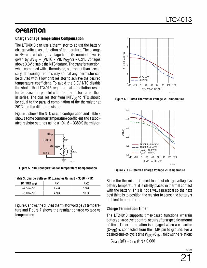
Charge Voltage Temperature Compensation
The LTC4013 can use a thermistor to adjust the battery charge voltage as a function of temperature. The change in FB-referred charge voltage from its nominal level is given by ∆VFB = (VNTC - VINTVCC/2) • 0.21. Voltages above 3.3V disable the NTC feature. The transfer function, when combined with a thermistor, is stronger than neces-sary. It is configured this way so that any thermistor can be diluted with a low drift resistor to achieve the desired temperature coefficient. To avoid the 3.3V NTC disable threshold, the LTC4013 requires that the dilution resis-tor be placed in parallel with the thermistor rather than in series. The bias resistor from INTVCC to NTC should be equal to the parallel combination of the thermistor at 25°C and the dilution resistor.
Figure 5 shows the NTC circuit configuration and Table 3 shows some common temperature coefficient and associ-ated resistor settings using a 10k, ß = 3380K thermistor.
OPERATION
Since the thermistor is used to adjust charge voltage vs battery temperature, it is ideally placed in thermal contact with the battery. This is not always practical so the next best thing is to position the resistor to sense the battery's ambient temperature.
Charge Termination Timer
The LTC4013 supports timer-based functions wherein battery charge cycle control occurs after a specific amount of time. Timer termination is engaged when a capacitor (CTMR) is connected from the TMR pin to ground. For a desired end-of-cycle time (tEOC) CTMR follows the relation:
CTMR (µF) = tEOC (Hr) • 0.066
Figure 5. NTC Configuration for Temperature Compensation
Figure 6. Diluted Thermistor Voltage vs Temperature
Figure 7. FB-Referred Charge Voltage vs Temperature
RN1
RNTC
RN2
4013 F05
LTC4013
NTC
INTVCC
SGND
Figure 6 shows the diluted thermistor voltage vs tempera-ture and Figure 7 shows the resultant charge voltage vs temperature.
−40 −20 0 20 40 60 80 100 120
TEMPERATURE (°C)
0
1
2
3
4
5
NTC
VOLT
AGE
(V)
4013 F06
−5mV/°C−2.5mV/°C
−40 −20 0 20 40 60 80 100 120
TEMPERATURE (°C)
1.6
1.8
2.0
2.2
2.4
2.6
VCH
(V)
4013 F07
FLOAT −5mV/°CFLOAT −2.5mV/°CABSORB −5mV/°CABSORB −2.5mV/°C
Table 3. Charge Voltage TC Examples Using ß = 3380 RNTCTC (WRT VFB) RN1 RN2
–2.5mV/°C 2.49k 3.32k
–5.0mV/°C 4.99k 10.0k
LTC4013
224013fa
OPERATIONTable 4. RT Resistor ValueSwitching Frequency RT (Ω)
1MHz 40.2k
750kHz 54.9k
500kHz 86.6k
300kHz 150k
200kHz 232k
The absorption and Li-Ion termination timer cycles start when the charger transitions from constant-current to constant-voltage charging. Equalization timing starts im-mediately upon transition to the equalization charge state and low battery timing commences when FB falls below LB.
Low Battery (LB) Pin
The LB pin is used to program the low battery level and is compared internally to the FB pin voltage. The LB pin sources a very precise 20µA current so the threshold volt-age can be programmed simply by placing a resistor from LB to ground. For instance, 100k to ground sets the LB pin to 2.0V. In 2-stage and Li-Ion charging a transition below the LB threshold triggers a new charge cycle if terminated. In 3-stage and 4-stage a transition below the LB threshold returns the charger to the absorption charging phase. In all four modes, Li-Ion, 2-stage, 3-stage and 4-stage, and with a timer capacitor present, the low battery fault timer starts and the charge current is reduced to C/5. All four modes terminate charging if the low-battery timer expires.
A commonly used low-battery voltage for a 6 cell battery is 10.4V which represents the voltage with one of 6 cells shorted. This LB voltage is set with an 86.6k resistor for 1.73V/cell, or 10.4V/6 with a 6-to-1 FB divider.
Output Current Monitoring
Charge current can be determined by observing the voltage at the ISMON pin. ISMON follows the expression:
ISMON = 20 • (VSENSE - VBAT).
Programming Switching Frequency
The LTC4013 has an operational switching frequency range between 200kHz and 1MHz which is programmed with an external resistor from the RT pin to ground. Table 4 shows resistor values and their corresponding switching frequencies. An approximate formula is:
RT(kΩ)= 40.2fSW
1.088 (MHz)
Switching Frequency Synchronization
The internal oscillator may also be synchronized to an external clock through the SYNC pin. The signal applied to the SYNC pin must have a logic low below 1.3V and a logic high above 1.7V. The input sync frequency must be 20% higher than the frequency that would otherwise be determined by the resistor at the RT pin. Input sig-nals outside of these specified parameters cause erratic switching behavior and subharmonic oscillations. When synchronizing to an external clock, be aware that there is a fixed delay from the input clock edge to the edge of the signal at the SW pin. Ground the SYNC pin if synchroniza-tion to an external clock is not required.
INFET Behavior
The LTC4013 controls an input N-Channel MOSFET via an on-chip charge pump on INFET. The MOSFET provides a blocking path to prevent battery discharge when the input voltage is below the battery voltage. It also disconnects the input supply from the charger to measure the input voltage with no load for Maximum Power Point Tracking (MPPT).
Undervoltage Lockouts
The INFET charge pump and switching regulator are enabled when all four UVLO comparators are satisfied and the ENAB pin is above its precision enable threshold. Specifically, VIN must be above its absolute threshold of 3.45V, DCIN must be greater than BAT by at least 99mV and must also be within 4mV of VIN. A fourth UVLO requires that the battery voltage at SENSE be above its UVLO level of approximately 1.97V.
LTC4013
234013fa
OPERATIONIf the conditions above are not met then INFET is turned off and sinks current pulling INFET to approximately 2.2V below the lower voltage of DCIN or VIN. If the input voltage is more than the gate breakdown of the external transistor, a TVS diode is required to prevent the disable current or pin leakage from pulling INFET all the way to ground. For MPPT applications requiring two transistors at INFET, a conventional diode will suffice as it will pull down the common source node safely.
Thermal Shutdown
The LTC4013 has thermal shutdown that disables charging at approximately 160°C. When the LTC4013 has cooled to 150°C, charging resumes. Thermal shutdown protects the device from excessive gate drive power and excess internal LDO power dissipation but does not necessarily prevent excess power dissipation in the external MOSFETS or other external components.
LTC4013
244013fa
Setting Charge Current
Charge current, ICHGMAX, is determined by the current sense resistor between SENSE and BAT. The servo voltage is 50mV making the charge current 50mV/RSENSE. For a 10A charge current RSENSE should be 5mΩ. Accuracy requires the use of 4-terminal sense resistors or care-ful attention to ensure a Kelvin connection to the sense resistor. Figure 18 shows two examples. Size the resistor for power dissipation with PRSENSE = ICHGMAX • 50mV. For example, the 10A sense resistor needs to be at least ½Watt. Susumu, Panasonic and Vishay offer a wide variety of accurate sense resistors.
Inductor Selection
Size the inductor so that the peak-to-peak ripple current is approximately 30% of the maximum charging current. This is a reasonable trade-off between inductor size and ripple. Inductance can be computed with the following equation:
L = VIN • VBAT – VBAT
2
0.3• fSW •ICHGMAX • VIN where VBAT is the battery voltage, VIN is the input voltage, ICHGMAX is the maximum charge current and fSW is the switching frequency. Choose the saturation current for the inductor to be at least 20% higher than the maximum charge current.
To protect against faults, there is an overcurrent compara-tor which terminates switching when the voltage between the SENSE and BAT pins exceeds 100mV. When tripped, switching is stopped for a minimum of 4 switch cycles.
Switching Regulator MOSFET Selection
Key parameters for MOSFET selection are: total gate charge (QG), on-resistance (RDS(ON)), gate to drain charge (QGD), gate-to-source charge (QGS), gate resistance (RG), breakdown voltage (maximum VGS and VDS) and drain current (maximum ID). The following guidelines provide information to make the selection process easier. Table 5 lists some recommended manufacturers.
APPLICATIONS INFORMATIONThe rated drain current for both MOSFETs must be greater than the maximum inductor current. Peak inductor current is approximately:
ILMAX = ICHGMAX +
VIN • VBAT – VBAT2
2• fSW •L • VIN
The rated drain current is temperature dependent, and most data sheets include a table or graph of rated drain current versus temperature.
The rated VDS must be higher than the maximum input voltage (including transients) for both MOSFETs.
The LTC4013 will drive the gates of the switching MOS-FETs with about 5V (INTVCC) with respect to their sources. However, during start-up and recovery conditions, the gate drive signals may be as low as 3V. Therefore, to ensure that the LTC4013 operates properly, use logic level thresh-old MOSFETs with a VT of about 2V or less. For a robust design, ensure that the rated maximum VGS is at least 7V.
Power loss in the switching MOSFETs is related to the on-resistance, RDS(ON); gate resistance, RG; gate-to-drain charge, QGD and gate-to-source charge, QGS. Power lost to the on-resistance is an ohmic loss, I²RDS(ON), and usually dominates for input voltages less than 15V. Power lost while charging the gate capacitance typically dominates for voltages greater than 15V. When operating at higher input voltages, efficiency is optimized by selecting a high side MOSFET with higher RDS(ON) and lower QG. The total power loss in the high side MOSFET is approximated by the sum of ohmic losses and transition losses:
PHIGH_LOSS =
VBATVIN
•IL2•RDS(ON) •ρT +
VIN •IL5V
•(QGD+QGS)•(2•RG+RPU+RPD)• fSW
ρT is a dimensionless temperature dependent factor in the MOSFET's on-resistance. Using 70°C as the maximum ambient operating temperature, ρT is roughly equal to 1.3. RPD and RPU are the LTC4013 high side gate driver output impedances: 2.3Ω and 1.3Ω, respectively.
LTC4013
254013fa
APPLICATIONS INFORMATIONFor the low side MOSFET the power loss is approximated by:
PLOW _LOSS = 1– VBATVIN
⎛
⎝⎜
⎞
⎠⎟•IL
2•RDS(ON) •ρT +
VIN •IL5V
• QGD+QGS( ) •(2•RG+RPU+RPD)• fSW
+Vf •2• fSW •IL• tnol
Where Vf is the voltage drop of the lower MOSFET bulk diode, typically 0.7V, and tnol is the non-overlap time, approximately 50ns. The last term in this expression represents the loss due to the body diode that is active during the non-overlap time.
In addition to the above requirements, it is desirable for the bottom MOSFET to have lower gate-drain capacitance as it minimizes coupling to BGATE when the SW pin rises. This coupling may momentarily turn on the bottom side MOSFET creating shoot-through that, at best, reduces efficiency and at worst can destroy the MOSFET.
While it is possible to get high and low side MOSFETs bonded in a common package, excessive power dissipation may require two separate packages or even that multiple high or low side MOSFETS be used at the high-power levels. Using multiple packages spreads the heat over a larger PCB area improving overall board temperature and efficiency.
At lower VIN, the top side MOSFET is on longer and low RDS(ON) helps lower dissipation but at higher input voltage the transient losses increase and can dominate. For the bottom side MOSFET the opposite is true. Optimization for best efficiency suggests different top and bottom MOSFETs.
A good approach to MOSFET sizing is to select the high side MOSFET first, then the low side MOSFET. The trade-off between RDS(ON), QG, and QGS for the high side MOSFET is evident in the following example of charging a 6 cell lead-acid battery from a 30V source at 20A. VBAT is equal to 14V, fSW = 200kHz.
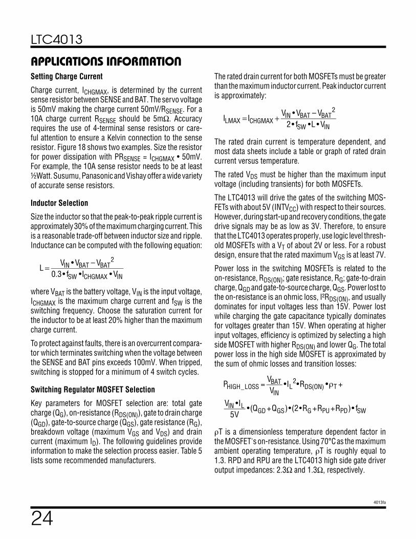
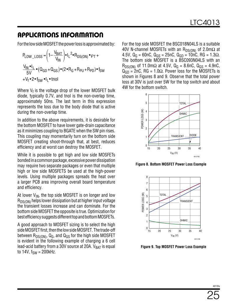
For the top side MOSFET the BSC018N04LS is a suitable 40V N-channel MOSFETs with an RDS(ON) of 2.0mΩ at 4.5V, QG = 60nC, QGS = 25nC, QGD = 10nC, RG = 1.3Ω. The bottom side MOSFET is a BSC093N04LS with an RDS(ON) of 11.0mΩ at 4.5V, QG = 8.6nC, QGS = 4.9nC, QGD = 2nC, RG = 1.0Ω. Power loss for the MOSFETs is shown in Figures 8 and 9. Observe that the total power loss at 30V is just over 5W for the top switch and about 4W for the bottom switch.
Figure 8. Bottom MOSFET Power Loss Example
Figure 9. Top MOSFET Power Loss Example
15 20 25 30 35 40
VIN (V)
0
1
2
3
4
5
6
POW
ER L
OSS
(W)
4013 F08
TOTAL
TRANSIENT
OHMIC
DiodeDiodeDiodeDIODE
15 20 25 30 35 40
VIN (V)
0
1
2
3
4
5
6
7
8
POW
ER L
OSS
(W)
4013 F09
TOTAL
TRANSIENT
OHMIC
LTC4013
264013fa
APPLICATIONS INFORMATION
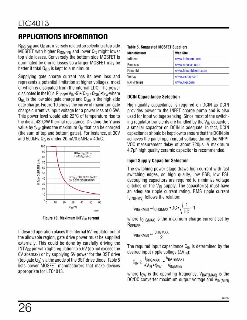
Figure 10. Maximum INTVCC current
RDS(ON) and QG are inversely related so selecting a top side MOSFET with higher RDS(ON) and lower QG might lower top side losses. Conversely the bottom side MOSFET is dominated by ohmic losses so a larger MOSFET may be better if total QGD is kept to a minimum.
Supplying gate charge current has its own loss and represents a potential limitation at higher voltages, most of which is dissipated from the internal LDO. The power dissipated in the IC is: PLDO=(VIN-5)•(QGL+QGH)•fSW where QGL is the low side gate charge and QGH is the high side gate charge. Figure 10 shows the curve of maximum gate charge current vs input voltage for a power loss of 0.5W. This power level would add 22°C of temperature rise to the die at 43°C/W thermal resistance. Dividing the Y axis value by fSW gives the maximum QG that can be charged (the sum of top and bottom gates). For instance, at 30V and 500kHz QG is under 20mA/0.5MHz = 40nC.
DCIN Capacitance Selection
High quality capacitance is required on DCIN as DCIN provides power to the INFET charge pump and is also used for input voltage sensing. Since most of the switch-ing regulator transients are handled by the VIN capacitor, a smaller capacitor on DCIN is adequate. In fact, DCIN capacitance should be kept low to ensure that the DCIN pin achieves the panel open circuit voltage during the MPPT VOC measurement delay of about 720μs. A maximum 4.7µF high quality ceramic capacitor is recommended.
Input Supply Capacitor Selection
The switching power stage draws high current with fast switching edges, so high quality, low ESR, low ESL decoupling capacitors are required to minimize voltage glitches on the VIN supply. The capacitor(s) must have an adequate ripple current rating. RMS ripple current IVIN(RMS) follows the relation:
IVIN(RMS) ≈ ICHGMAX •DC• 1
DC–1
where ICHGMAX is the maximum charge current set by RSENSE.
IVIN(RMS) ≈ICHGMAX
2
The required input capacitance CIN is determined by the desired input ripple voltage (∆VIN):
CIN ≥ ICHGMAXΔVIN • fSW
•VBAT(MAX)
VIN(MIN)
where fSW is the operating frequency, VBAT(MAX) is the DC/DC converter maximum output voltage and VIN(MIN)
If desired operation places the internal 5V regulator out of the allowable region, gate drive power must be supplied externally. This could be done by carefully driving the INTVCC pin with tight regulation to 5.5V (do not exceed the 6V absmax) or by supplying 5V power for the BST drive (top gate QG) via the anode of the BST drive diode. Table 5 lists power MOSFET manufacturers that make devices appropriate for LTC4013.
Table 5. Suggested MOSFET SuppliersManufacturer Web Site
Infineon www.infineon.com
Renesas www.renesas.com
Fairchild www.fairchildsemi.com
Vishay www.vishay.com
NXP/Philips www.nxp.com
0 10 20 30 40 50 60
VIN (V)
0
10
20
30
40
50
60
70
80
90
100
INTV
CC C
URRE
NT (m
A)
4013 F10
TOTAL G Q (nC) = sw I(mA)/f (MHz)
INTVCC CURRENT BASEDON 0.5W DISSIPATION
LTC4013
274013fa
APPLICATIONS INFORMATIONis the minimum input operating voltage. Keeping ∆VIN below 100mV is a good starting point. As an example, let ICHGMAX = 10A, ∆VIN = 0.1V, fSW = 500k, VBAT(MAX) = 15V, VIN(MIN) = 18V then CIN is greater than 167µF.
Meeting these requirements at higher voltages may require multiple capacitors and possibly a mixture of capacitor types. Because of the fast switching edges it is important that the total decoupling capacitance have low ESR and ESL to avoid sharp voltage spikes. The best practice is to use several low-ESR ceramic capacitors as part of the capacitance, with higher density capacitors utilized for bulk requirements. X7R capacitors tend to maintain their capacitance over a wide range of operating voltages and temperatures. Minimize the loop created by the input ca-pacitor, the high side MOSFET and the low side MOSFET to reduce radiation components. See Linear Technology application notes AN139 and AN144 for more information on EMI.
Battery Capacitor Selection
The output of the charger is the battery which represents a large effective capacitance. Because the battery often has significant wiring connecting it to the charger, additional decoupling output capacitors at the charger are needed. The BAT node is also used for voltage sensing so better performance is obtained with lower voltage ripple at the BAT and FB pins. The BAT capacitor needs to have low ESR to reduce output ripple. To achieve the lowest possible ESR, use several low-ESR ceramic capacitors in parallel. Lower output voltage applications may benefit from the use of high density POSCAP capacitors which are easily destroyed when exposed to over-voltage conditions. To prevent this, select POSCAP capacitors that have a voltage rating that is at least 20% higher than the regulated voltage.
The ripple current on these capacitors is the same as the inductor ripple. Since, in general, inductor selection is chosen to have ripple current equal to or below 30% of ICHGMAX, an adequate ripple current rating for the BAT capacitor(s) is 0.4 • ICHGMAX. The capacitors also need to be surge rated to the maximum output current.
Sizing for output ripple voltage is similar to input decou-pling:
CBAT ≥0.4•ICHGMAXΔVBAT • fSW
For example, if ICHGMAX = 10A, ∆VBAT = 0.1V, fSW = 500k then choose CBAT greater than 80µF.
INTVCC LDO Output, and BST Supply
INTVCC provides power to the LTC4103 but also provides charge to the gate drives. The boosted supply pin allows the use of an N-channel top MOSFET switch for increased conversion efficiency and lower cost. The BST capacitor is connected from SW to BST with a low leakage 1A Schottky diode connected from INTVCC to BST. The diode must be rated for a reverse voltage greater than the input supply voltage maximum.
CBST is sized to hold the BST rail reasonably constant when delivering gate charge to the MOSFET. A good rule of thumb is:
CBST >50 • QGHVGS
=10 •QGH
where QGH is the top side MOSFET QG at 5V.
For example, if the top gate charge is 20nC charged to INTVCC at 5V, then keep the CBST capacitance larger than 0.2µF.
CBST is charged during the bottom switch on time. The LTC4013 maintains a minimum top gate off time to provide this charge. If the LTC4013 is in discontinuous mode with the bottom switch off and the boost voltage drops, the bottom side switch is enabled to provide BST capacitor charging.
Since BST capacitor charge current is drawn from the INTVCC capacitor, CBST needs to be sized to have minimal drop during recharge. A good starting point for high-current MOSFETs with high gate charge is to set CINTVCC larger than 4.7µF. Connect it as close as possible to the exposed pad underneath the package. Because of the fast high-current edges, use a low-ESR ceramic capacitor with ESR typically lower than 20mΩ. For driving MOSFETs with gate charge larger than 44nC, size INTVCC with 0.5µF/nC of total gate charge (top plus bottom MOSFETs).
LTC4013
284013fa
Figure 11. ENAB Resistor Divider
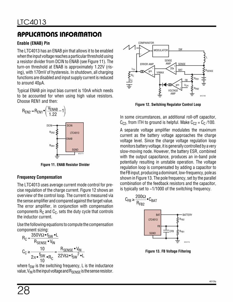
Figure 12. Switching Regulator Control Loop
Figure 13. FB Voltage Filtering
APPLICATIONS INFORMATIONEnable (ENAB) Pin
The LTC4013 has an ENAB pin that allows it to be enabled when the input voltage reaches a particular threshold using a resistor divider from DCIN to ENAB (see Figure 11). The turn-on threshold at ENAB is approximately 1.22V (ris-ing), with 170mV of hysteresis. In shutdown, all charging functions are disabled and input supply current is reduced to around 40μA.
Typical ENAB pin input bias current is 10nA which needs to be accounted for when using high value resistors. Choose REN1 and then:
REN2 =REN1• VENAB1.22
–1⎛
⎝⎜
⎞
⎠⎟
Frequency Compensation
The LTC4013 uses average current mode control for pre-cise regulation of the charge current. Figure 12 shows an overview of the control loop. The current is measured via the sense amplifier and compared against the target value. The error amplifier, in conjunction with compensation components RC and CC, sets the duty cycle that controls the inductor current.
Use the following equations to compute the compensation component sizing:
RC =350VΩ • fSW •L
RSENSE • VIN
CC ≥10
2π • fSW10
•RC
=RSENSE • VIN
22VΩ • fSW2 •L
where fSW is the switching frequency, L is the inductance value, VIN is the input voltage and RSENSE is the sense resistor.
In some circumstances, an additional roll-off capacitor, CC2, from ITH to ground is helpful. Make CC2 = CC /100.
A separate voltage amplifier modulates the maximum current as the battery voltage approaches the charge voltage level. Since the charge voltage regulation loop monitors battery voltage, it is generally controlled by a very slow-moving node. However, the battery ESR, combined with the output capacitance, produces an in-band pole potentially resulting in unstable operation. The voltage regulation loop is compensated by adding a capacitor to the FB input, producing a dominant, low-frequency, pole as shown in Figure 13. The pole frequency, set by the parallel combination of the feedback resistors and the capacitor, is typically set to ~1/1000 of the switching frequency.
CFB ≥
200ΩRFB2
•CBAT
DCIN
REN1
REN2 LTC4013
ENAB
DCIN
SGND4013 F11
VIMAX
VCH
ITH
SENSE
BAT
SW
FB
RSENSE–
+gm
CC
+
–20x
+
–
COMPARATOR
+
–gm
RC
L
RFB1
RFB2
MODULATOR
ERROR AMPSENSEAMP
VOLTAGEAMP
4013 F09
BATTERY
4013 F13
RFB2
RFB1CFB
LTC4013
FB
BAT
SGND
LTC4013
294013fa
Figure 14. Resistor Divider for MPPT
APPLICATIONS INFORMATIONMaximum Power Point Tracking (MPPT)
MPPT is used to regulate the input voltage to maximize power transfer from a power limited source. The first step is to determine the maximum power voltage. For a solar panel, this can be determined from the data sheet. A resistor divider between the input source and the FBOC and MPPT pins is used to program the LTC4013 to regu-late the input source at its maximum power voltage. The FBOC pin is used to sample the input source open circuit voltage when charging is paused while the MPPT pin is used to regulate the maximum power voltage when the charger is running. The MPPT resistor divider should be configured as shown in Figure 14.
the ratio of the DCIN voltage at regulation and open circuit as KR gives:
VDCIN(MP)
VDCIN(OC)=
RMP1RMP1+RMP2
=KR
This equation can be written to solve for RMP2 as a func-tion of RMP1 and the DCIN ratio KR:
RMP2 =RMP1• 1KR
–1⎛
⎝⎜
⎞
⎠⎟
Substituting that for RMP2 in the equation for KF and solving for RMP3:
RMP3 =RMP1• 1KF
– 1KR
⎛
⎝⎜
⎞
⎠⎟
The design procedure is:
1. Choose RMP1 such that VFBOC = 1.0V to 3.0V. Current in the resistor string of 5μA to 50μA is recommended.
2. Calculate RMP2 based on RMP1 and the ratio, KR, between the maximum power voltage and the open circuit voltage.
3. Calculate RMP3 based on RMP1, and the KR and KF ratios.
As an example, consider a solar panel with an open circuit voltage VDCIN(OC) = 24V and a maximum power voltage VDCIN(MP) = 17V. Choose VFBOC = 1.5V. Then calculate:
KF =1.5V24V
=0.0625
KR =17V24V
=0.708
RMP1=1.5V30µA
=50k (Choose 30µA inDivider)
RMP2 =50k • 10.708
–1⎛
⎝⎜
⎞
⎠⎟=20.6k
RMP3 =50k • 10.0625
– 10.708
⎛
⎝⎜
⎞
⎠⎟=729k
As another example, consider charging a battery from a source with an open-circuit voltage of 30V and a source impedance of 5Ω. This resistive supply has a short circuit
DCIN
RMP2
RMP1
RMP3LTC4013
MPPT
DCIN
SGND
FBOC
4013 F13
Choose the attenuation ratio of FBOC to DCIN (KF) so VFBOC is between 1.0V and 3.0V when the input voltage is at its highest (i.e. open circuit, VDCIN(OC)). The attenu-ation ratio of MPPT to DCIN is set so that VMPPT equals the chosen VFBOC when DCIN is at the maximum power voltage, VDCIN(MP). The following equations define those conditions:
VFBOCVDCIN(OC)
= RMP1RMP1+ RMP2 + RMP3
=KF
VMPPTVDCIN(MP)
= RMP1+RMP2RMP1 + RMP2 + RMP3
When the MPPT loop is in regulation, the MPPT voltage equals the FBOC voltage as measured during the open circuit interval. Reworking the above equations to define
LTC4013
304013fa
APPLICATIONS INFORMATIONcurrent of 6A, and the peak available power of 45W occurs with a load of 3A at 50% of VOC. MPPT settings would have VDCIN(OC) = 30V, VFBOC = 1.5V,
KF =VFBOC
VDCIN(OC)=
1.5V30V
=0.05
KR =VDCIN(MP)
VDCIN(OC)=
15V30V
=0.5
Again with 30µA in RMP1, RMP1 = 50k then
RMP2 = 50k •1
0.5–1⎛
⎝⎜⎞⎠⎟ = 50k and
RMP3 = 50k •1
0.05–
10.5
⎛⎝⎜
⎞⎠⎟ = 900k
If the MPPT function is not needed, it can be disabled by tying FBOC to INTVCC.
Additional MPPT Considerations
MPPT operation requires the use of back-to-back MOSFETs for the input PowerPath to allow open circuit DCIN voltage measurement. When using back-to-back MOSFETs the sources are tied together, drains on the outside. A single MOSFET cannot be used because the body diode clamps DCIN to VIN when the input MOSFET is off, resulting in incorrect measurement of the DCIN open circuit voltage.
Because MPPT operation involves large changes in input voltage, ensure that the programmed maximum power voltage is greater than both 4.5V and is at least 100mV above the battery voltage.
A lead capacitor, CMPPT, from DCIN to MPPT can com-pensate the input voltage regulation loop during MPPT operation.
Battery Stacks
Batteries are often stacked serially to increase voltage and reduce current. The LTC4013 charges voltage stacks of up to 60V. However, when stacking cells or a battery of cells, cell/battery balancing should be employed. Omitting cell balancing can quickly result in a degenerate scenario of rapidly diverging cell voltages with possible cell failure over several charge-discharge cycles.
Plugging in a Battery
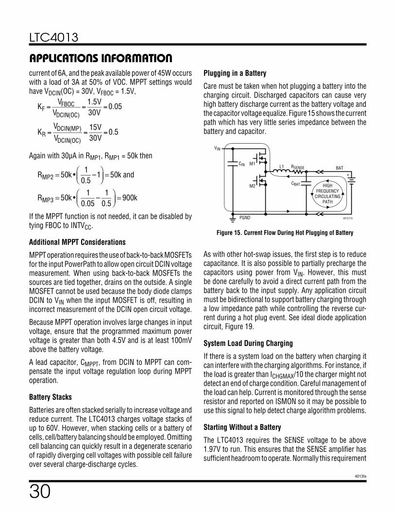
Care must be taken when hot plugging a battery into the charging circuit. Discharged capacitors can cause very high battery discharge current as the battery voltage and the capacitor voltage equalize. Figure 15 shows the current path which has very little series impedance between the battery and capacitor.
VIN
CIN L1 RSENSE
M2
PGND 4013 F15
CBAT
BAT+
M1
HIGHFREQUENCY
CIRCULATINGPATH
Figure 15. Current Flow During Hot Plugging of Battery
As with other hot-swap issues, the first step is to reduce capacitance. It is also possible to partially precharge the capacitors using power from VIN. However, this must be done carefully to avoid a direct current path from the battery back to the input supply. Any application circuit must be bidirectional to support battery charging through a low impedance path while controlling the reverse cur-rent during a hot plug event. See ideal diode application circuit, Figure 19.
System Load During Charging
If there is a system load on the battery when charging it can interfere with the charging algorithms. For instance, if the load is greater than ICHGMAX/10 the charger might not detect an end of charge condition. Careful management of the load can help. Current is monitored through the sense resistor and reported on ISMON so it may be possible to use this signal to help detect charge algorithm problems.
Starting Without a Battery
The LTC4013 requires the SENSE voltage to be above 1.97V to run. This ensures that the SENSE amplifier has sufficient headroom to operate. Normally this requirement
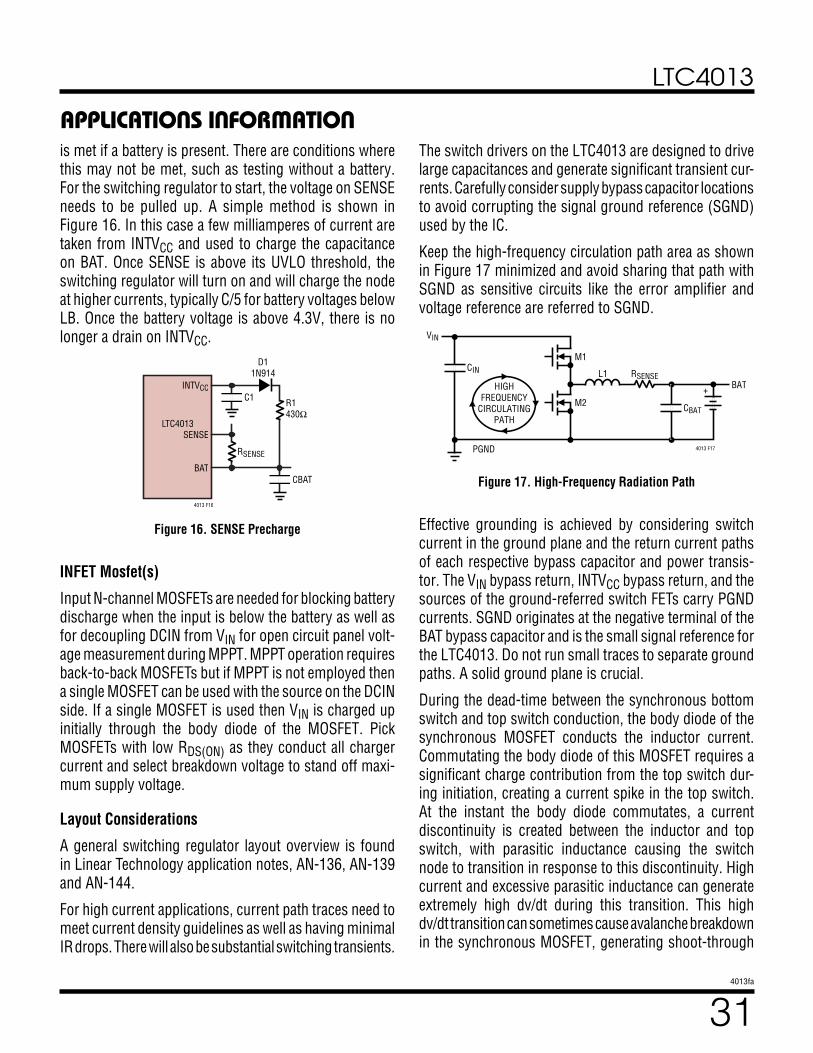
LTC4013
314013fa
APPLICATIONS INFORMATIONis met if a battery is present. There are conditions where this may not be met, such as testing without a battery. For the switching regulator to start, the voltage on SENSE needs to be pulled up. A simple method is shown in Figure 16. In this case a few milliamperes of current are taken from INTVCC and used to charge the capacitance on BAT. Once SENSE is above its UVLO threshold, the switching regulator will turn on and will charge the node at higher currents, typically C/5 for battery voltages below LB. Once the battery voltage is above 4.3V, there is no longer a drain on INTVCC.
The switch drivers on the LTC4013 are designed to drive large capacitances and generate significant transient cur-rents. Carefully consider supply bypass capacitor locations to avoid corrupting the signal ground reference (SGND) used by the IC.
Keep the high-frequency circulation path area as shown in Figure 17 minimized and avoid sharing that path with SGND as sensitive circuits like the error amplifier and voltage reference are referred to SGND.
R1430Ω
CBAT
C1
RSENSE
D11N914
LTC4013SENSE
INTVCC
BAT
4013 F16
Figure 16. SENSE Precharge
INFET Mosfet(s)
Input N-channel MOSFETs are needed for blocking battery discharge when the input is below the battery as well as for decoupling DCIN from VIN for open circuit panel volt-age measurement during MPPT. MPPT operation requires back-to-back MOSFETs but if MPPT is not employed then a single MOSFET can be used with the source on the DCIN side. If a single MOSFET is used then VIN is charged up initially through the body diode of the MOSFET. Pick MOSFETs with low RDS(ON) as they conduct all charger current and select breakdown voltage to stand off maxi-mum supply voltage.
Layout Considerations
A general switching regulator layout overview is found in Linear Technology application notes, AN-136, AN-139 and AN-144.
For high current applications, current path traces need to meet current density guidelines as well as having minimal IR drops. There will also be substantial switching transients.
VIN
CIN L1 RSENSE
M2
4013 F17
CBAT
BAT+
M1
HIGHFREQUENCY
CIRCULATINGPATH
PGND
Figure 17. High-Frequency Radiation Path
Effective grounding is achieved by considering switch current in the ground plane and the return current paths of each respective bypass capacitor and power transis-tor. The VIN bypass return, INTVCC bypass return, and the sources of the ground-referred switch FETs carry PGND currents. SGND originates at the negative terminal of the BAT bypass capacitor and is the small signal reference for the LTC4013. Do not run small traces to separate ground paths. A solid ground plane is crucial.
During the dead-time between the synchronous bottom switch and top switch conduction, the body diode of the synchronous MOSFET conducts the inductor current. Commutating the body diode of this MOSFET requires a significant charge contribution from the top switch dur-ing initiation, creating a current spike in the top switch. At the instant the body diode commutates, a current discontinuity is created between the inductor and top switch, with parasitic inductance causing the switch node to transition in response to this discontinuity. High current and excessive parasitic inductance can generate extremely high dv/dt during this transition. This high dv/dt transition can sometimes cause avalanche breakdown in the synchronous MOSFET, generating shoot-through
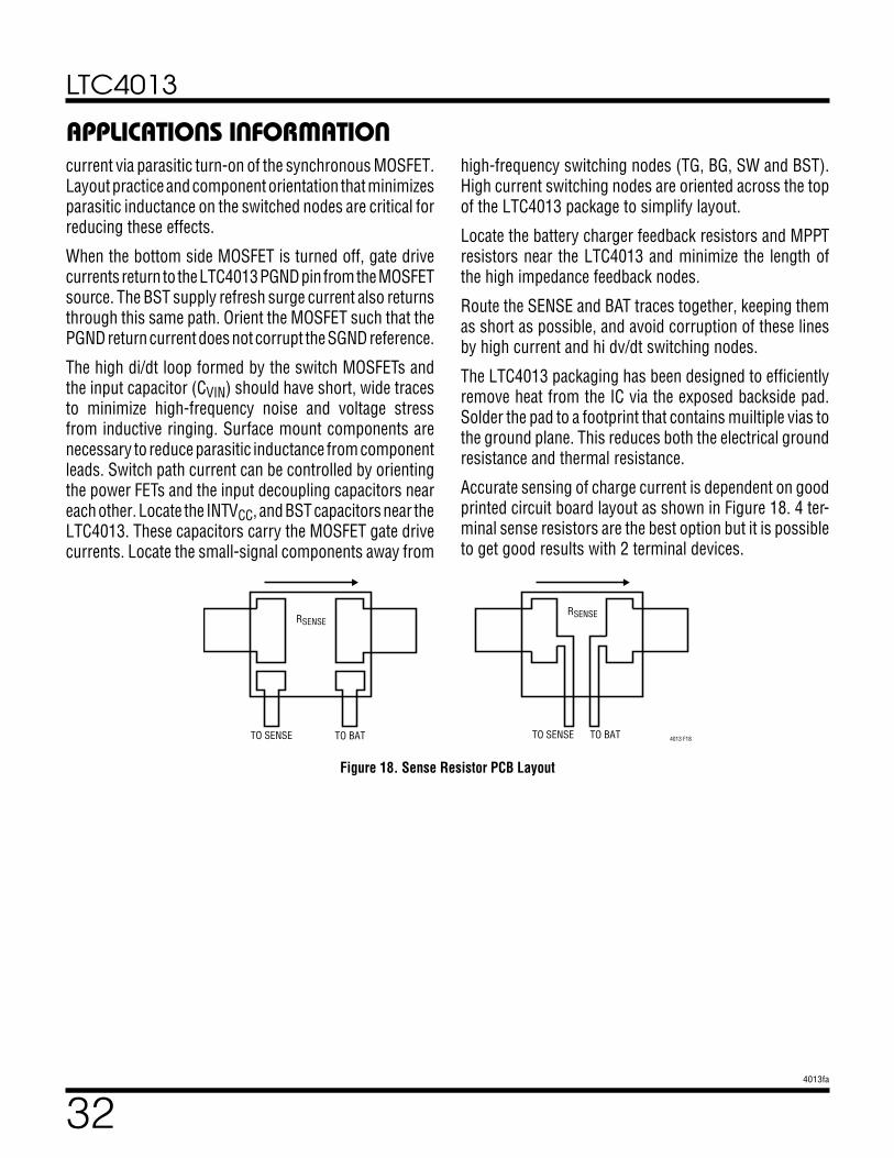
LTC4013
324013fa
APPLICATIONS INFORMATIONcurrent via parasitic turn-on of the synchronous MOSFET. Layout practice and component orientation that minimizes parasitic inductance on the switched nodes are critical for reducing these effects.
When the bottom side MOSFET is turned off, gate drive currents return to the LTC4013 PGND pin from the MOSFET source. The BST supply refresh surge current also returns through this same path. Orient the MOSFET such that the PGND return current does not corrupt the SGND reference.
The high di/dt loop formed by the switch MOSFETs and the input capacitor (CVIN) should have short, wide traces to minimize high-frequency noise and voltage stress from inductive ringing. Surface mount components are necessary to reduce parasitic inductance from component leads. Switch path current can be controlled by orienting the power FETs and the input decoupling capacitors near each other. Locate the INTVCC, and BST capacitors near the LTC4013. These capacitors carry the MOSFET gate drive currents. Locate the small-signal components away from
high-frequency switching nodes (TG, BG, SW and BST). High current switching nodes are oriented across the top of the LTC4013 package to simplify layout.
Locate the battery charger feedback resistors and MPPT resistors near the LTC4013 and minimize the length of the high impedance feedback nodes.
Route the SENSE and BAT traces together, keeping them as short as possible, and avoid corruption of these lines by high current and hi dv/dt switching nodes.
The LTC4013 packaging has been designed to efficiently remove heat from the IC via the exposed backside pad. Solder the pad to a footprint that contains muiltiple vias to the ground plane. This reduces both the electrical ground resistance and thermal resistance.
Accurate sensing of charge current is dependent on good printed circuit board layout as shown in Figure 18. 4 ter-minal sense resistors are the best option but it is possible to get good results with 2 terminal devices.
RSENSE
TO SENSE TO BAT 4013 F18
RSENSE
TO SENSE TO BAT
Figure 18. Sense Resistor PCB Layout
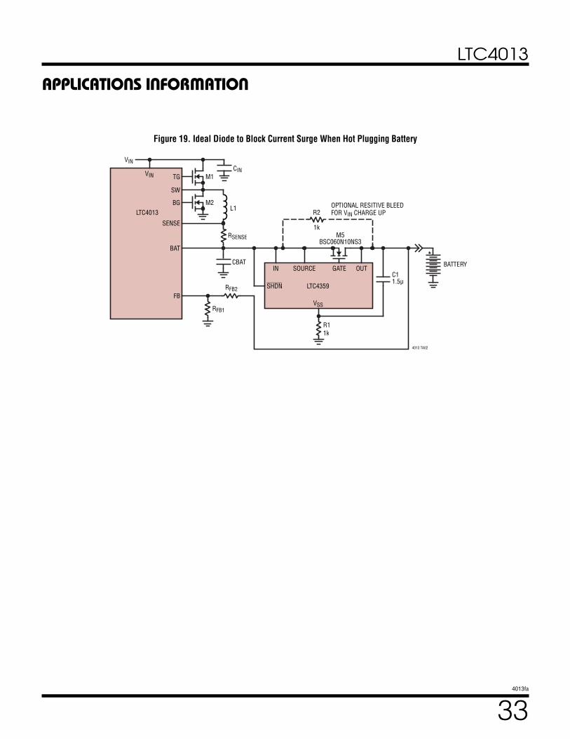
LTC4013
334013fa
APPLICATIONS INFORMATION
Figure 19. Ideal Diode to Block Current Surge When Hot Plugging Battery
VIN
M5BSC060N10NS3
C11.5µ
R11k
R2
1k
OUTGATESOURCEIN
SHDN
VSS
LTC4359
L1
CBAT
RSENSE
RFB1
RFB2
BATTERY
4013 TA02
M1
M2
CIN
BAT
SENSE
BG
SW
TGVIN
FB
LTC4013OPTIONAL RESITIVE BLEED FOR VIN CHARGE UP
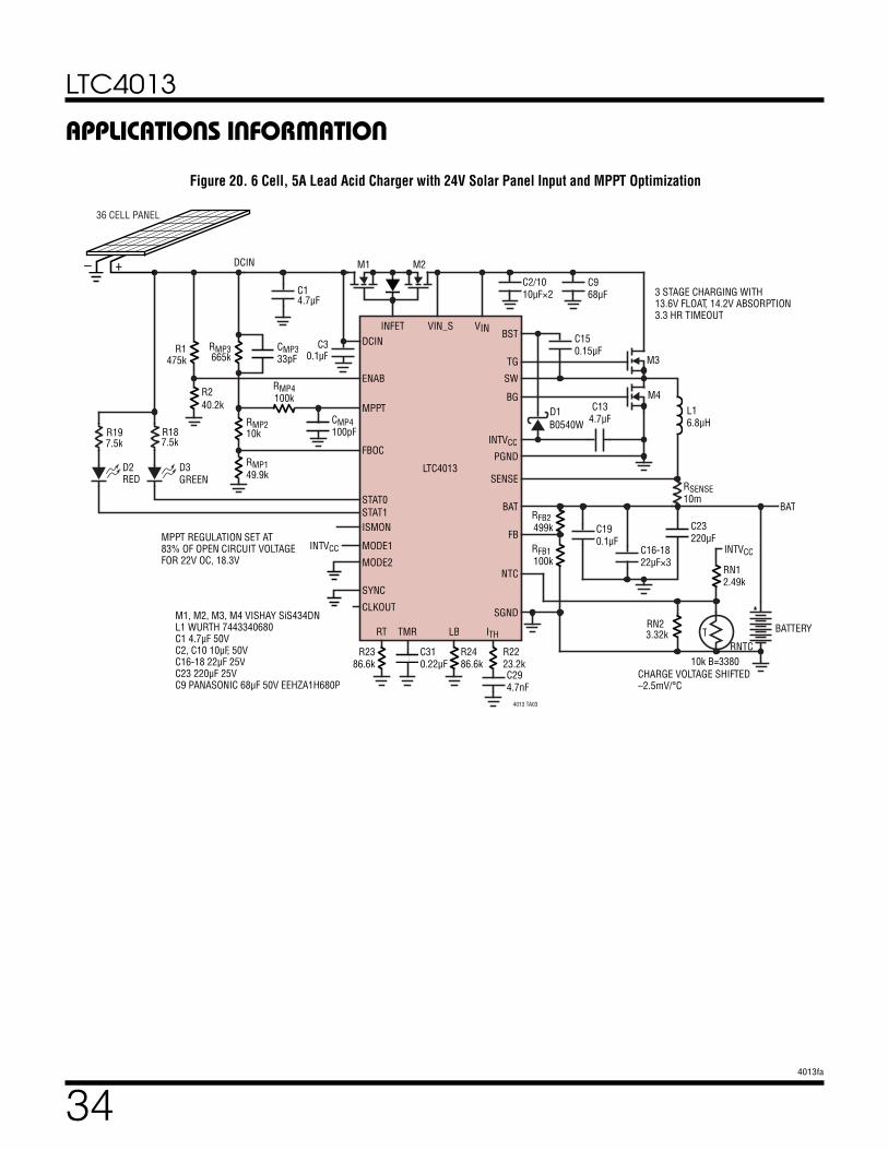
LTC4013
344013fa
APPLICATIONS INFORMATION
Figure 20. 6 Cell, 5A Lead Acid Charger with 24V Solar Panel Input and MPPT Optimization
INTVCC
BAT
BATTERY
DCIN
INTVCC
D1B0540W
DCIN
ENAB
INTVCC
SYNC
SGND
SENSE
BAT
ITHRT
CLKOUT
PGND
FB
TG
SW
BST
BG
VIN
FBOC
MPPT
INFET
LB
NTC
MODE1
MODE2
VIN_S
STAT1STAT0
TMR
ISMON
LTC4013
4013 TA03
M1 M2
M3
M4
C14.7µF
C294.7nF
R2223.2k
R2486.6k
R2386.6k
C310.22µF
RSENSE10m
RFB2499k
RFB1100k
C16-1822µF×3
C23220µF
C190.1µF
C134.7µF
L16.8µH
R187.5k
D3GREEN
R197.5k
D2RED
R1475k
R240.2k
C30.1µF
CMP4100pF
C150.15µF
C968µF
C2/1010µF×2
RMP2
CMP333pF
10k
RMP4100k
RMP149.9k
RMP3665k
10k B=3380RNTC
T
RN12.49k
RN23.32k
M1, M2, M3, M4 VISHAY SiS434DNL1 WURTH 7443340680C1 4.7µF 50V C2, C10 10µF, 50VC16-18 22µF 25VC23 220µF 25VC9 PANASONIC 68µF 50V EEHZA1H680P
3 STAGE CHARGING WITH 13.6V FLOAT, 14.2V ABSORPTION3.3 HR TIMEOUT
MPPT REGULATION SET AT 83% OF OPEN CIRCUIT VOLTAGEFOR 22V OC, 18.3V
CHARGE VOLTAGE SHIFTED–2.5mV/°C
+–
36 CELL PANEL
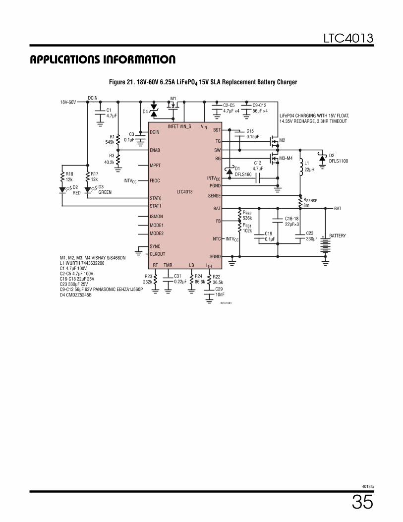
LTC4013
354013fa
APPLICATIONS INFORMATION
Figure 21. 18V-60V 6.25A LiFePO4 15V SLA Replacement Battery Charger
18V-60V
INTVCC
INTVCC
BAT
DCIN
D1DFLS160
DCIN
ENAB
INTVCC
SYNC
SGND
SENSE
BAT
ITHRT
CLKOUT
PGND
FB
TG
SW
BST
BG
VIN
FBOC
MPPT
INFET
LB
NTC
MODE1
MODE2
VIN_S
STAT1
STAT0
TMR
ISMON
LTC4013
BATTERY
4013 TA04
M1
M2
D2DFLS1100M3-M4
C14.7µF
C2910nF
R2236.5k
R2486.6k
R23232k
C310.22µF
RSENSE8m
RFB2536kRFB1102k
C16-1822µF×3
C23330µF
C190.1µF
C134.7µF
L122µH
R1712k
D3GREEN
R1812k
D2RED
R1549k
R340.2k
C30.1µF
C150.15µF
C9-C1256µF ×4
C2-C54.7µF ×4
M1, M2, M3, M4 VISHAY SiS468DNL1 WURTH 7443632200C1 4.7µF 100V C2-C5 4.7µF, 100VC16-C18 22µF 25VC23 330µF 25VC9-C12 56µF 63V PANASONIC EEHZA1J560PD4 CMDZZ5245B
LiFeP04 CHARGING WITH 15V FLOAT,14.35V RECHARGE, 3.3HR TIMEOUT
D4
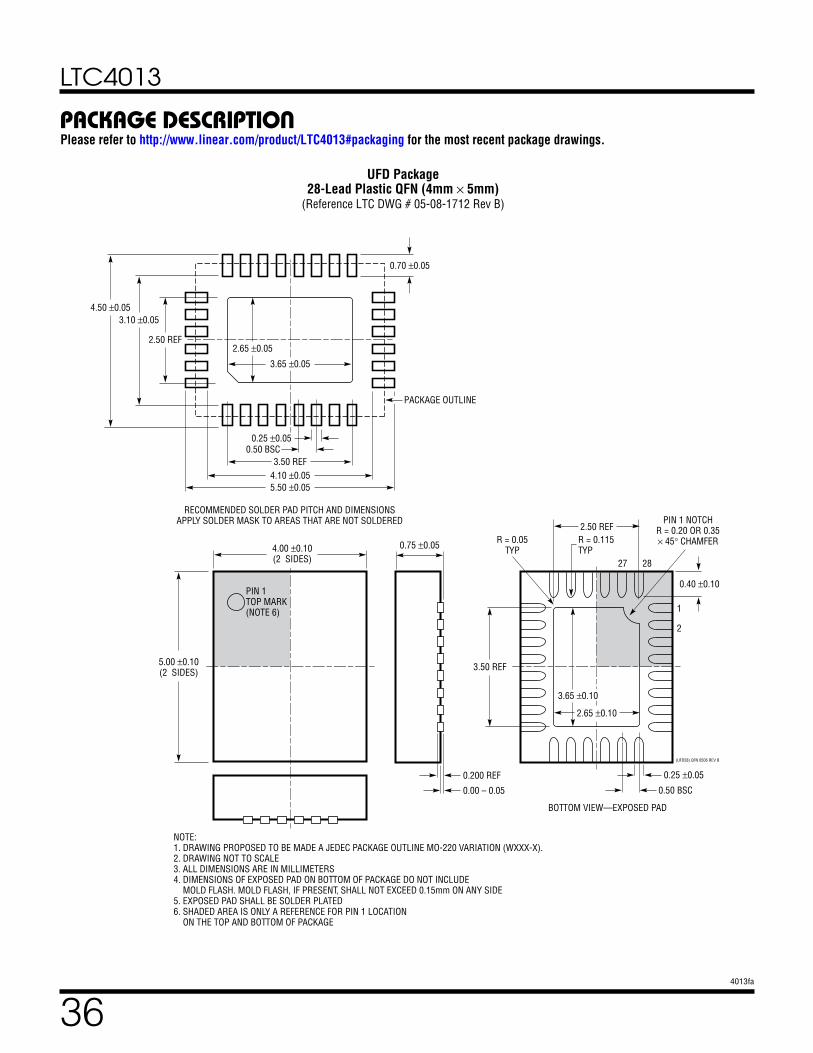
LTC4013
364013fa
PACKAGE DESCRIPTIONPlease refer to http://www.linear.com/product/LTC4013#packaging for the most recent package drawings.
4.00 ±0.10(2 SIDES)
2.50 REF
5.00 ±0.10(2 SIDES)
NOTE:1. DRAWING PROPOSED TO BE MADE A JEDEC PACKAGE OUTLINE MO-220 VARIATION (WXXX-X).2. DRAWING NOT TO SCALE3. ALL DIMENSIONS ARE IN MILLIMETERS4. DIMENSIONS OF EXPOSED PAD ON BOTTOM OF PACKAGE DO NOT INCLUDE MOLD FLASH. MOLD FLASH, IF PRESENT, SHALL NOT EXCEED 0.15mm ON ANY SIDE5. EXPOSED PAD SHALL BE SOLDER PLATED6. SHADED AREA IS ONLY A REFERENCE FOR PIN 1 LOCATION ON THE TOP AND BOTTOM OF PACKAGE
PIN 1TOP MARK(NOTE 6)
0.40 ±0.10
27 28
1
2
BOTTOM VIEW—EXPOSED PAD
3.50 REF
0.75 ±0.05 R = 0.115TYP
R = 0.05TYP
PIN 1 NOTCHR = 0.20 OR 0.35× 45° CHAMFER
0.25 ±0.05
0.50 BSC
0.200 REF
0.00 – 0.05
(UFD28) QFN 0506 REV B
RECOMMENDED SOLDER PAD PITCH AND DIMENSIONSAPPLY SOLDER MASK TO AREAS THAT ARE NOT SOLDERED
0.70 ±0.05
0.25 ±0.050.50 BSC
2.50 REF
3.50 REF4.10 ±0.055.50 ±0.05
2.65 ±0.05
3.10 ±0.054.50 ±0.05
PACKAGE OUTLINE
2.65 ±0.10
3.65 ±0.10
3.65 ±0.05
UFD Package28-Lead Plastic QFN (4mm × 5mm)
(Reference LTC DWG # 05-08-1712 Rev B)
LTC4013
374013fa
Information furnished by Linear Technology Corporation is believed to be accurate and reliable. However, no responsibility is assumed for its use. Linear Technology Corporation makes no representa-tion that the interconnection of its circuits as described herein will not infringe on existing patent rights.
REVISION HISTORYREV DATE DESCRIPTION PAGE NUMBER
A 02/18 Added min value to Battery Voltage Range (BAT) spec
Segregated Charger State Diagram by Mode
Clarified Device Operation
3
17-20
1-38
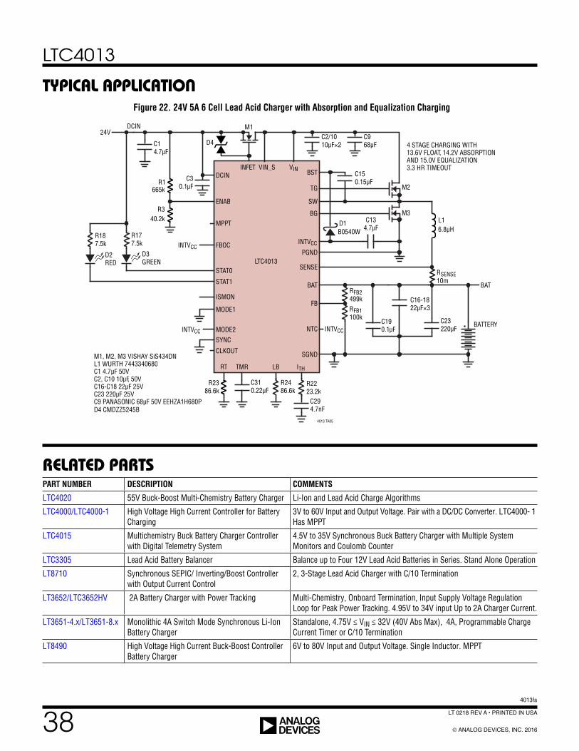
LTC4013
384013fa
ANALOG DEVICES, INC. 2016
LT 0218 REV A • PRINTED IN USA
RELATED PARTS
TYPICAL APPLICATION
PART NUMBER DESCRIPTION COMMENTS
LTC4020 55V Buck-Boost Multi-Chemistry Battery Charger Li-Ion and Lead Acid Charge Algorithms
LTC4000/LTC4000-1 High Voltage High Current Controller for Battery Charging
3V to 60V Input and Output Voltage. Pair with a DC/DC Converter. LTC4000- 1 Has MPPT
LTC4015 Multichemistry Buck Battery Charger Controller with Digital Telemetry System
4.5V to 35V Synchronous Buck Battery Charger with Multiple System Monitors and Coulomb Counter
LTC3305 Lead Acid Battery Balancer Balance up to Four 12V Lead Acid Batteries in Series. Stand Alone Operation
LT8710 Synchronous SEPIC/ Inverting/Boost Controller with Output Current Control
2, 3-Stage Lead Acid Charger with C/10 Termination
LT3652/LTC3652HV 2A Battery Charger with Power Tracking Multi-Chemistry, Onboard Termination, Input Supply Voltage Regulation Loop for Peak Power Tracking. 4.95V to 34V input Up to 2A Charger Current.
LT3651-4.x/LT3651-8.x Monolithic 4A Switch Mode Synchronous Li-Ion Battery Charger
Standalone, 4.75V ≤ VIN ≤ 32V (40V Abs Max), 4A, Programmable Charge Current Timer or C/10 Termination
LT8490 High Voltage High Current Buck-Boost Controller Battery Charger
6V to 80V Input and Output Voltage. Single Inductor. MPPT
Figure 22. 24V 5A 6 Cell Lead Acid Charger with Absorption and Equalization Charging
INTVCC
24V
INTVCC
INTVCC
BAT
DCIN
D1B0540W
DCIN
ENAB
INTVCC
SYNC
SGND
SENSE
BAT
ITHRT
CLKOUT
PGND
FB
TG
SW
BST
BG
VIN
FBOC
MPPT
INFET
LB
NTC
MODE1
MODE2
VIN_S
STAT1
STAT0
TMR
ISMON
LTC4013
BATTERY
4013 TA05
M1
M2
M3
C14.7µF
C294.7nF
R2223.2k
R2486.6k
R2386.6k
C310.22µF
RSENSE10m
RFB2499kRFB1100k
C16-1822µF×3
C23220µF
C190.1µF
C134.7µF
L16.8µH
R177.5k
D3GREEN
R187.5k
D2RED
R1665k
R340.2k
C30.1µF
C150.15µF
C968µF
C2/1010µF×2
M1, M2, M3 VISHAY SiS434DNL1 WURTH 7443340680C1 4.7µF 50V C2, C10 10µF, 50VC16-C18 22µF 25VC23 220µF 25VC9 PANASONIC 68µF 50V EEHZA1H680PD4 CMDZZ5245B
4 STAGE CHARGING WITH 13.6V FLOAT, 14.2V ABSORPTIONAND 15.0V EQUALIZATION3.3 HR TIMEOUT
D4


![STANDOX MAZDA 2010 [Kompatibilitätsmodus] · MAZDA MODELS / MODELLE 01 VIN / TYPENSCHILD VIN PLATE LOCATION PREMACY VIN PLATE MAZDA PAINTCODE = 18G VIN PLATE MAZDA PAINTCODE = 2X](https://img.pdfslide.net/doc/110x75/5e8fcc3177ae5012020ddb18/standox-mazda-2010-kompatibilittsmodus-mazda-models-modelle-01-vin-typenschild.jpg)