Embed Size (px)
Citation preview
LTC4155
14155fd
For more information www.linear.com/LTC4155
Typical applicaTion
FeaTures DescripTion
Dual-Input Power Manager/3.5A Li-Ion Battery Charger with
I2C Control and USB OTG
The LTC®4155 is a 15 watt I2C controlled power manager with PowerPath™ instant-on operation, high efficiency switching battery charging and USB compatibility. The LTC4155 seamlessly manages power distribution from two 5V sources, such as a USB port and a wall adapter, to a single-cell rechargeable Lithium-Ion/Polymer battery and a system load.
The LTC4155’s switching battery charger automatically limits its input current for USB compatibility, or may draw up to 3A from a high power wall adapter. The high efficiency step-down switching charger is designed to provide maximum power to the application and reduced heat in high power density applications.
I2C adjustability of input current, charge current, battery float voltage, charge termination, and many other param-eters allows maximum flexibility. I2C status reporting of key system and charge parameters facilitates intelligent control decisions. USB On-The-Go support provides 5V power back to the USB port without any additional com-ponents. A dual-input, priority multiplexing, overvoltage protection circuit guards the LTC4155 from high voltage damage on the VBUS pin.
The LTC4155 is available in the low profile (0.75mm) 28-lead 4mm × 5mm QFN surface mount package.
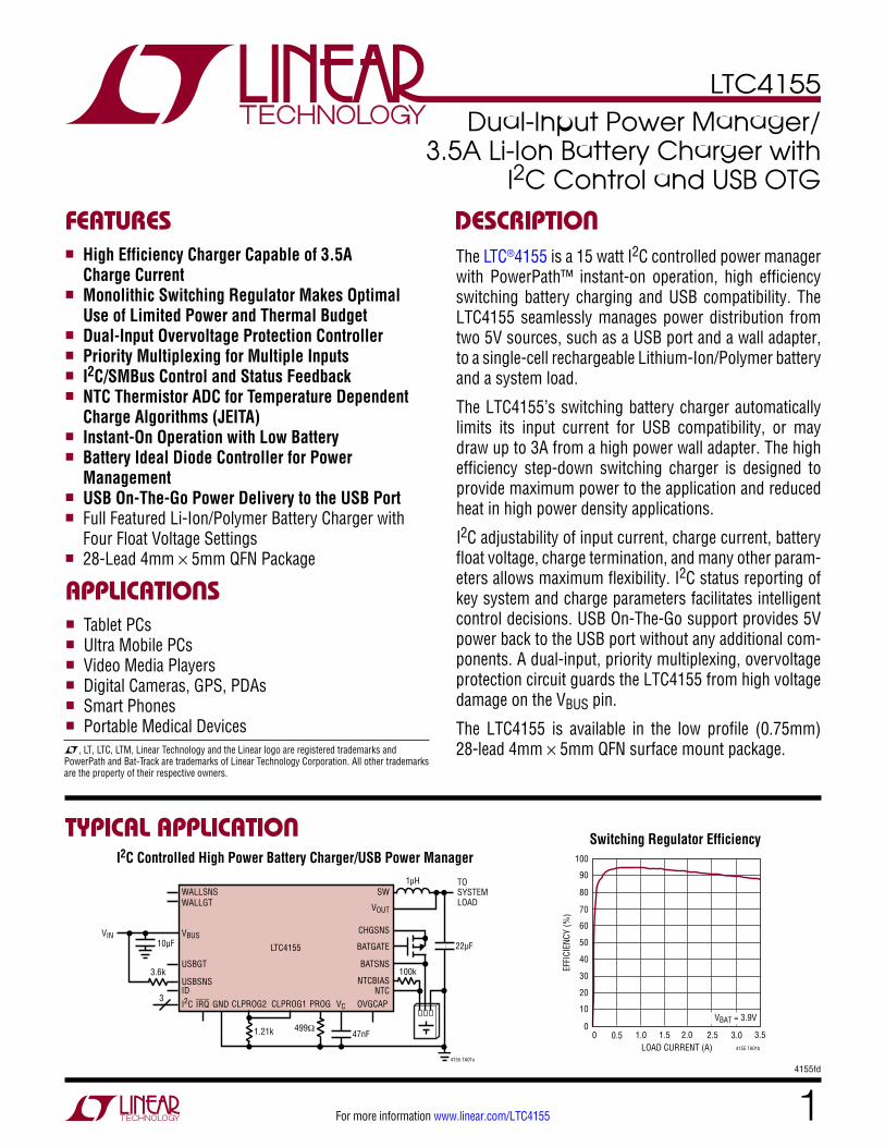
I2C Controlled High Power Battery Charger/USB Power Manager
applicaTions
n High Efficiency Charger Capable of 3.5A Charge Current
n Monolithic Switching Regulator Makes Optimal Use of Limited Power and Thermal Budget
n Dual-Input Overvoltage Protection Controllern Priority Multiplexing for Multiple Inputsn I2C/SMBus Control and Status Feedbackn NTC Thermistor ADC for Temperature Dependent
Charge Algorithms (JEITA)n Instant-On Operation with Low Batteryn Battery Ideal Diode Controller for Power
Managementn USB On-The-Go Power Delivery to the USB Portn Full Featured Li-Ion/Polymer Battery Charger with
Four Float Voltage Settingsn 28-Lead 4mm × 5mm QFN Package
n Tablet PCsn Ultra Mobile PCsn Video Media Playersn Digital Cameras, GPS, PDAsn Smart Phonesn Portable Medical DevicesL, LT, LTC, LTM, Linear Technology and the Linear logo are registered trademarks and PowerPath and Bat-Track are trademarks of Linear Technology Corporation. All other trademarks are the property of their respective owners.
VBUSVIN
CLPROG1CLPROG2 PROG VC OVGCAPIRQI2C GND3
3.6k 100k
ID
USBGT
CHGSNS
USBSNS
1.21k 499Ω47nF
10µF 22µF
NTC
BATSNS
BATGATE
NTCBIAS
WALLGT
LTC4155
WALLSNS
VOUT
SWTOSYSTEMLOAD
1µH
4155 TA01a
LOAD CURRENT (A)0
0
EFFI
CIEN
CY (%
)
10
30
40
50
100
70
1.0 2.0 2.54155 TA01b
20
80
90
60
0.5 1.5 3.0 3.5
VBAT = 3.9V
Switching Regulator Efficiency
LTC4155
24155fd
For more information www.linear.com/LTC4155
Table oF conTenTs Features ............................................................................................................................ 1Applications ....................................................................................................................... 1Typical Application ............................................................................................................... 1Description......................................................................................................................... 1Absolute Maximum Ratings ..................................................................................................... 3Order Information ................................................................................................................. 3Pin Configuration ................................................................................................................. 3Electrical Characteristics ........................................................................................................ 4Typical Performance Characteristics .......................................................................................... 9Pin Functions .....................................................................................................................12Block Diagram ....................................................................................................................15Timing Diagrams ................................................................................................................16Operation..........................................................................................................................17
I2C ........................................................................................................................................................................ 17Applications Information .......................................................................................................40Typical Applications .............................................................................................................47Package Description ............................................................................................................51Typical Application ..............................................................................................................52Related Parts .....................................................................................................................52
LTC4155
34155fd
For more information www.linear.com/LTC4155
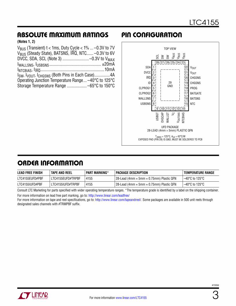
pin conFiguraTionabsoluTe MaxiMuM raTings
VBUS (Transient) t < 1ms, Duty Cycle < 1% ... –0.3V to 7VVBUS (Steady State), BATSNS, IRQ, NTC ...... –0.3V to 6VDVCC, SDA, SCL (Note 3) ........................–0.3V to VMAXIWALLSNS, IUSBSNS ............................................... ±20mAINTCBIAS, IIRQ ..........................................................10mAISW, IVOUT, ICHGSNS (Both Pins in Each Case) ..............4AOperating Junction Temperature Range ... –40°C to 125°CStorage Temperature Range .................. –65°C to 150°C
(Notes 1, 2)
9 10
TOP VIEW
29GND
UFD PACKAGE28-LEAD (4mm × 5mm) PLASTIC QFN
11 12 13
28 27 26 25 24
14
23
6
5
4
3
2
1SDA
DVCC
IRQ
ID
CLPROG1
CLPROG2
WALLSNS
USBSNS
VOUT
VOUT
CHGSNS
CHGSNS
PROG
BATGATE
BATSNS
NTC
SCL
SW SW V BUS
V BUS
V BUS
USBG
T
OVGC
AP
WAL
LGT V C
V OUT
SNS
NTCB
IAS
7
17
18
19
20
21
22
16
8 15
TJMAX = 125°C, θJA = 43°C/W
EXPOSED PAD (PIN 29) IS GND, MUST BE SOLDERED TO PCB
orDer inForMaTionLEAD FREE FINISH TAPE AND REEL PART MARKING* PACKAGE DESCRIPTION TEMPERATURE RANGE
LTC4155EUFD#PBF LTC4155EUFD#TRPBF 4155 28-Lead (4mm × 5mm × 0.75mm) Plastic QFN –40°C to 125°C
LTC4155IUFD#PBF LTC4155IUFD#TRPBF 4155 28-Lead (4mm × 5mm × 0.75mm) Plastic QFN –40°C to 125°C
Consult LTC Marketing for parts specified with wider operating temperature ranges. *The temperature grade is identified by a label on the shipping container.For more information on lead free part marking, go to: http://www.linear.com/leadfree/ For more information on tape and reel specifications, go to: http://www.linear.com/tapeandreel/. Some packages are available in 500 unit reels through designated sales channels with #TRMPBF suffix.
LTC4155
44155fd
For more information www.linear.com/LTC4155
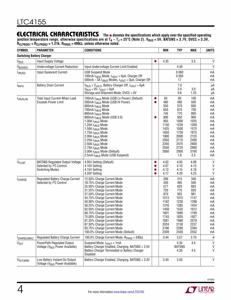
The l denotes the specifications which apply over the specified operating junction temperature range, otherwise specifications are at TA ≈ TJ = 25°C (Note 2). VBUS = 5V, BATSNS = 3.7V, DVCC = 3.3V, RCLPROG1 = RCLPROG2 = 1.21k, RPROG = 499Ω, unless otherwise noted.
elecTrical characTerisTics
SYMBOL PARAMETER CONDITIONS MIN TYP MAX UNITS
Switching Battery Charger
VBUS Input Supply Voltage l 4.35 5.5 V
VBUSREG Undervoltage Current Reduction Input Undervoltage Current Limit Enabled 4.30 V
IVBUSQ Input Quiescent Current USB Suspend Mode 100mA IVBUS Mode, IVOUT = 0µA, Charger Off 500mA – 3A IVBUS Modes, IVOUT = 0µA, Charger Off
0.060 0.560
17
mA mA mA
IBATQ Battery Drain Current VBUS > VUVLO, Battery Charger Off, IVOUT = 0µA VBUS = 0V, IVOUT = 0µA Storage and Shipment Mode, DVCC = 0V
7.0 2.0 0.6
3.0
1.25
µA µA µA
IVBUSLIM Total Input Current When Load Exceeds Power Limit
100mA IVBUS Mode (USB Lo Power) (Default) 500mA IVBUS Mode (USB Hi Power) 600mA IVBUS Mode 700mA IVBUS Mode 800mA IVBUS Mode 900mA IVBUS Mode (USB 3.0) 1.00A IVBUS Mode 1.25A IVBUS Mode 1.50A IVBUS Mode 1.75A IVBUS Mode 2.00A IVBUS Mode 2.25A IVBUS Mode 2.50A IVBUS Mode 2.75A IVBUS Mode 3.00A IVBUS Mode (Default) 2.5mA IVBUS Mode (USB Suspend)
l
l
l
65 460 550 650 745 800 950
1150 1425 1650 1900 2050 2350 2550 2800
80 480 570 670 770 850
1000 1230 1500 1750 2000 2175 2475 2725 2950 1.8
100 500 600 700 800 900
1025 1300 1575 1875 2125 2300 2600 2900 3100 2.5
mA mA mA mA mA mA mA mA mA mA mA mA mA mA mA mA
VFLOAT BATSNS Regulated Output Voltage Selected by I2C Control. Switching Modes
4.05V Setting (Default) 4.10V Setting 4.15V Setting 4.20V Setting
l
l
l
l
4.02 4.07 4.12 4.17
4.05 4.10 4.15 4.20
4.08 4.13 4.18 4.23
V V V V
ICHARGE Regulated Battery Charge Current Selected by I2C Control
12.50% Charge Current Mode 18.75% Charge Current Mode 25.00% Charge Current Mode 31.25% Charge Current Mode 37.50% Charge Current Mode 43.75% Charge Current Mode 50.00% Charge Current Mode 56.25% Charge Current Mode 62.50% Charge Current Mode 68.75% Charge Current Mode 75.00% Charge Current Mode 81.25% Charge Current Mode 87.50% Charge Current Mode 93.75% Charge Current Mode 100.0% Charge Current Mode (Default)
290 430 577 720 870
1013 1162 1316 1458 1601 1743 1881 2024 2166 2309
315 465 620 770 925
1075 1230 1385 1535 1685 1835 1980 2130 2280 2430
340 500 663 820 981
1137 1298 1454 1612 1769 1927 2079 2237 2394 2552
mA mA mA mA mA mA mA mA mA mA mA mA mA mA mA
ICHARGE(MAX) Regulated Battery Charge Current 100.0% Charge Current Mode, RPROG = 340Ω 3.44 3.57 3.70 A
VOUT PowerPath Regulated Output Voltage (VBUS Power Available)
Suspend Mode, IVOUT = 1mA Battery Charger Enabled, Charging, BATSNS ≥ 3.5V Battery Charger Terminated or Battery Charger Disabled
4.35 BATSNS
4.35
4.5
4.5
V V V
VOUT(MIN) Low Battery Instant-On Output Voltage (VBUS Power Available)
Battery Charger Enabled, Charging, BATSNS ≤ 3.3V 3.40 3.50 V
LTC4155
54155fd
For more information www.linear.com/LTC4155
elecTrical characTerisTics The l denotes the specifications which apply over the specified operating junction temperature range, otherwise specifications are at TA ≈ TJ = 25°C (Note 2). VBUS = 5V, BATSNS = 3.7V, DVCC = 3.3V, RCLPROG1 = RCLPROG2 = 1.21k, RPROG = 499Ω, unless otherwise noted.
SYMBOL PARAMETER CONDITIONS MIN TYP MAX UNITS
IVOUT VOUT Current Available Before Loading Battery
2.5mA IVBUS Mode (USB Suspend) 100mA IVBUS Mode, BAT = 3.3V 500mA IVBUS Mode, BAT = 3.3V 600mA IVBUS Mode, BAT = 3.3V 700mA IVBUS Mode, BAT = 3.3V 800mA IVBUS Mode, BAT = 3.3V 900mA IVBUS Mode, BAT = 3.3V 1.00A IVBUS Mode, BAT = 3.3V 1.25A IVBUS Mode, BAT = 3.3V 1.50A IVBUS Mode, BAT = 3.3V 1.75A IVBUS Mode, BAT = 3.3V 2.00A IVBUS Mode, BAT = 3.3V 2.25A IVBUS Mode, BAT = 3.3V 2.50A IVBUS Mode, BAT = 3.3V 2.75A IVBUS Mode, BAT = 3.3V 3.00A IVBUS Mode, BAT = 3.3V
1 1.3 76
673 810 944
1093 1200 1397 1728 2072 2411 2700 2846 3154 3408 3657
mA mA mA mA mA mA mA mA mA mA mA mA mA mA mA mA
VPROG PROG Pin Servo Voltage 12.50% Charge Current Mode 18.75% Charge Current Mode 25.00% Charge Current Mode 31.25% Charge Current Mode 37.50% Charge Current Mode 43.75% Charge Current Mode 50.00% Charge Current Mode 56.25% Charge Current Mode 62.50% Charge Current Mode 68.75% Charge Current Mode 75.00% Charge Current Mode 81.25% Charge Current Mode 87.50% Charge Current Mode 93.75% Charge Current Mode 100.0% Charge Current Mode (Default)
150 225 300 375 450 525 600 675 750 825 900 975
1050 1125 1200
mV mV mV mV mV mV mV mV mV mV mV mV mV mV mV
VRECHRG Recharge Battery Threshold Voltage
Threshold Voltage Relative to VFLOAT 96.6 97.6 98.4 %
tTERMINATE Safety Timer Termination Period Selected by I2C Control. Timer Starts When BATSNS ≥ VFLOAT
1-Hour Mode 2-Hour Mode 4-Hour Mode (Default) 8-Hour Mode
0.95 1.90 3.81 7.63
1.06 2.12 4.24 8.48
1.17 2.33 4.66 9.32
Hours Hours Hours Hours
VLOWBAT Threshold Voltage Rising Threshold Hysteresis
2.65 2.8 130
2.95 V mV
tBADBAT Bad Battery Termination Time BATSNS < (VLOWBAT – ΔVLOWBAT) 0.47 0.53 0.59 Hours
VC/x Full Capacity Charge Indication PROG Voltage Selected by I2C Control
C/10 Mode (ICHARGE = 10%FS) (Default) C/5 Mode (ICHARGE = 20%FS) C/20 Mode (ICHARGE = 5%FS) C/50 Mode (ICHARGE = 2%FS)
110 230 15 50
120 240 24 60
130 250 33 70
mV mV mV mV
hPROG Ratio of ICHGSNS to PROG Pin Current
1000 mA/mA
hCLPROG1 (Note 4)
Ratio of Measured VBUS Current to CLPROG1 Sense Current
CLPROG1 IVBUS Mode 990 mA/mA
LTC4155
64155fd
For more information www.linear.com/LTC4155
elecTrical characTerisTics The l denotes the specifications which apply over the specified operating junction temperature range, otherwise specifications are at TA ≈ TJ = 25°C (Note 2). VBUS = 5V, BATSNS = 3.7V, DVCC = 3.3V, RCLPROG1 = RCLPROG2 = 1.21k, RPROG = 499Ω, unless otherwise noted.
SYMBOL PARAMETER CONDITIONS MIN TYP MAX UNITS
hCLPROG2 (Note 4)
Ratio of Measured VBUS Current to CLPROG2 Sense Current
2.5mA IVBUS Mode (USB Suspend) 100mA IVBUS Mode 500mA IVBUS Mode 600mA IVBUS Mode 700mA IVBUS Mode 800mA IVBUS Mode 900mA IVBUS Mode 1.00A IVBUS Mode 1.25A IVBUS Mode 1.50A IVBUS Mode 1.75A IVBUS Mode 2.00A IVBUS Mode 2.25A IVBUS Mode 2.50A IVBUS Mode 2.75A IVBUS Mode 3.00A IVBUS Mode
19 79
466 557 657 758 839 990
1222 1494 1746 1999 2175 2477 2730 2956
mA/mA mA/mA mA/mA mA/mA mA/mA mA/mA mA/mA mA/mA mA/mA mA/mA mA/mA mA/mA mA/mA mA/mA mA/mA mA/mA
VCLPROG1 CLPROG1 Servo Voltage in Current Limit
CLPROG1 IVBUS Mode 1.2 V
VCLPROG2 CLPROG2 Servo Voltage in Current Limit
2.5mA IVBUS Mode (USB Suspend) 100mA – 3A IVBUS Modes
103 1.2
mV V
fOSC Switching Frequency 2.05 2.25 2.50 MHz
RPMOS High Side Switch On Resistance 0.090 Ω
RNMOS Low Side Switch On Resistance 0.080 Ω
RCHG Battery Charger Current Sense Resistance
0.040 Ω
IPEAK Peak Inductor Current Clamp 500mA – 3A IVBUS Modes 6.7 A
Step-Up Mode PowerPath Switching Regulator (USB On-The-Go)
VBUS Output Voltage 0mA ≤ IVBUS ≤ 500mA 4.75 5.25 V
VOUT Input Voltage 2.9 V
IVBUSOTG Output Current Limit 1.4 A
IVOUTOTGQ VOUT Quiescent Current IVBUS = 0mA 1.96 mA
VCLPROG2 Output Current Limit Servo Voltage 1.2 V
VBATSNSUVLO VBATSNS Undervoltage Lockout VBATSNS Falling Hysteresis
2.65 2.8 130
2.95 V mV
tSCFAULT Short-Circuit Fault Delay VBUS < 4V 7.2 ms
Overvoltage Protection, Priority Multiplexer and Undervoltage Lockout; USB Input Connected to USBSNS Through 3.6k Resistor; WALL Input Connected to WALLSNS Through 3.6k Resistor
VUVLO USB Input, Wall Input Undervoltage Lockout
Rising Threshold Falling Threshold Hysteresis
4.05 3.90
100
4.45 4.25
V V
mV
VDUVLO USB Input, Wall Input to BATSNS Differential Undervoltage Lockout
Rising Threshold Falling Threshold Hysteresis
100 50
70
425 375
mV mV mV
VOVLO USB Input, Wall Input Overvoltage Protection Threshold
Rising Threshold 5.75 6.0 6.3 V
VUSBGTACTV USBGT Output Voltage Active USBSNS < VUSBOVLO 2 • VUSBSNS V
VWALLGTACTV WALLGT Output Voltage Active WALLSNS < VWALLOVLO 2 • VWALLSNS V
VUSBGTPROT USBGT Output Voltage Protected USBSNS > VUSBOVLO 0 V
LTC4155
74155fd
For more information www.linear.com/LTC4155
elecTrical characTerisTics The l denotes the specifications which apply over the specified operating junction temperature range, otherwise specifications are at TA ≈ TJ = 25°C (Note 2). VBUS = 5V, BATSNS = 3.7V, DVCC = 3.3V, RCLPROG1 = RCLPROG2 = 1.21k, RPROG = 499Ω, unless otherwise noted.
SYMBOL PARAMETER CONDITIONS MIN TYP MAX UNITS
VWALLGTPROT WALLGT Output Voltage Protected WALLSNS > VWALLOVLO 0 V
VUSBGTLOAD, VWALLGTLOAD
USBGT, WALLGT Voltage Under Load
5V Through 3.6k into WALLSNS, USBSNS, IUSBGT, IWALLGT = 1µA
8.4 8.9 V
IUSBSNSQ USBSNS Quiescent Current VUSBSNS = 5V, VUSBSNS > VWALLSNS VUSBSNS = 5V, VWALLSNS > VUSBSNS
27 54
µA µA
IWALLSNSQ WALLSNS Quiescent Current VWALLSNS = 5V, VWALLSNS > VUSBSNS VWALLSNS = 5V, VUSBSNS > VWALLSNS
27 54
µA µA
tRISE OVGCAP Time to Reach Regulation COVGCAP = 1nF 1.2 ms
IRQ Pin Characteristics
IIRQ IRQ Pin Leakage Current VIRQ = 5V 1 µA
VIRQ IRQ Pin Output Low Voltage IIRQ = 5mA 75 100 mV
ID Pin Characteristics
IID ID Pin Pull-Up Current VID = 0V 35 55 85 μA
VID_OTG ID Pin Threshold Voltage ID Pin Falling Hysteresis
0.5 0.86 0.2
0.95 V V
Overtemperature Battery Conditioner
IBATOVERTEMP Overtemp Battery Discharge Current
Only When Enabled via I2C Control 125 mA
VBATOVERTEMP Overtemp Battery Voltage Target Only When Enabled via I2C Control 3.85 V
Thermistor Measurement System
kOFFSET VNTC / VNTCBIAS A/D Lower Range End
VNTC / VNTCBIAS Ratio Below Which Only 0x00 Is Returned
0.113 V/V
kHIGH VNTC / VNTCBIAS A/D Upper Range End
VNTC / VNTCBIAS Ratio Above Which Only 0x7F Is Returned
0.895 V/V
kSPAN A/D Span Coefficient (Decimal Format)
6.091 6.162 6.191 mV/V/LSB
dTOO_COLD NTCVAL at NTC_TOO_COLD (Decimal Format)
Warning Threshold Reset Threshold
102 98
102 98
102 98
Count Count
dTOO_WARM NTCVAL at NTC_TOO_WARM (Decimal Format)
Warning Threshold Reset Threshold
41 45
41 45
41 45
Count Count
dHOT_FAULT NTCVAL at HOT_FAULT (Decimal Format)
Fault Threshold Reset Threshold
19 23
19 23
19 23
Count Count
INTC NTC Leakage Current –100 100 nA
Ideal Diode
VFWD Forward Voltage Detection Input Power Available, Battery Charger Off 15 mV
I2C Port
DVCC I2C Logic Reference Level (Note 3) 1.7 VMAX V
IDVCCQ DVCC Current SCL/SDA = 0kHz 0.25 µA
VDVCC_UVLO DVCC UVLO 1.0 V
ADDRESS I2C Address 0001_001[R/W]b
VIH,SDA,SCL Input High Threshold 70 % DVCC
VIL,SDA,SCL Input Low Threshold 30 % DVCC
IIH,SDA,SCL Input Leakage High SDA, SCL = DVCC –1 1 µA
LTC4155
84155fd
For more information www.linear.com/LTC4155
elecTrical characTerisTics The l denotes the specifications which apply over the specified operating junction temperature range, otherwise specifications are at TA ≈ TJ = 25°C (Note 2). VBUS = 5V, BATSNS = 3.7V, DVCC = 3.3V, RCLPROG1 = RCLPROG2 = 1.21k, RPROG = 499Ω, unless otherwise noted.
SYMBOL PARAMETER CONDITIONS MIN TYP MAX UNITS
IIL,SDA,SCL Input Leakage Low SDA, SCL = 0V –1 1 µA
VOL Digital Output Low (SDA) ISDA = 3mA 0.4 V
fSCL Clock Operating Frequency 400 kHz
tBUF Bus Free Time Between STOP and START Condition
1.3 µs
tHD_SDA Hold Time After (Repeated) START Condition
0.6 µs
tSU_SDA Repeated START Condition Set-Up Time
0.6 µs
tSU_STO STOP Condition Time 0.6 µs
tHD_DAT(OUT) Data Hold Time 0 900 ns
tHD_DAT(IN) Input Data Hold Time 0 ns
tSU_DAT Data Set-Up Time 100 ns
tLOW Clock LOW Period 1.3 µs
tHIGH Clock HIGH Period 0.6 µs
tf Clock Data Fall Time 20 300 ns
tr Clock Data Rise Time 20 300 ns
tSP Spike Suppression Time 50 ns
Note 1: Stresses beyond those listed under Absolute Maximum Ratings may cause permanent damage to the device. Exposure to any Absolute Maximum Rating condition for extended periods may affect device reliability and lifetime.Note 2: The LTC4155E is tested under pulsed load conditions such that TJ ≈ TA. The LTC4155E is guaranteed to meet performance specifications from 0°C to 85°C junction temperature. Specifications over the –40°C to 125°C operating junction temperature range are assured by design, characterization and correlation with statistical process controls. The LTC4155I is guaranteed over the full –40°C to 125°C operating junction temperature range. The junction temperature (TJ, in °C) is
calculated from the ambient temperature (TA, in °C) and power dissipation (PD, in watts) according to the formula: TJ = TA + (PD • θJA), where the package thermal impedance θJA = 43°C/W)Note that the maximum ambient temperature consistent with these specifications is determined by specific operating conditions in conjunction with board layout, the rated package thermal resistance and other environmental factors.Note 3. VMAX is the maximum of VBUS or BATSNSNote 4. Total input current is IVBUSQ + VCLPROG/RCLPROG • (hCLPROG + 1).
LTC4155
94155fd
For more information www.linear.com/LTC4155
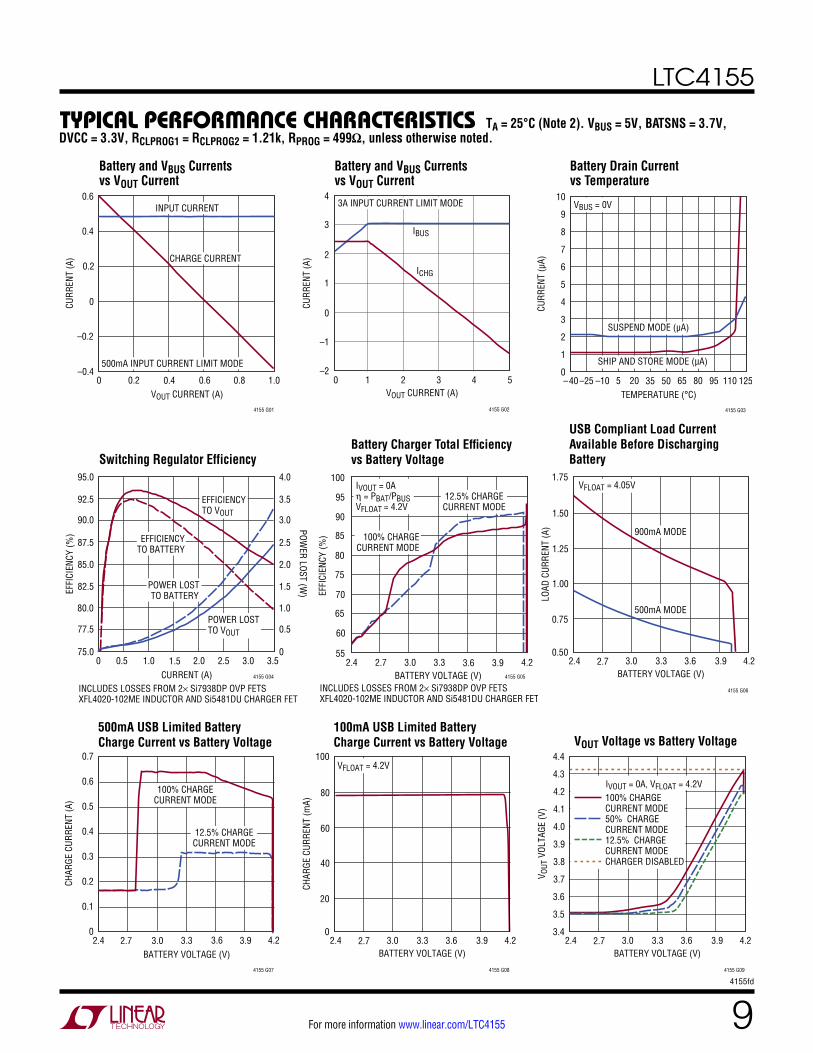
Typical perForMance characTerisTics
Switching Regulator EfficiencyBattery Charger Total Efficiency vs Battery Voltage
Battery and VBUS Currents vs VOUT Current
Battery and VBUS Currents vs VOUT Current
Battery Drain Current vs Temperature
VOUT CURRENT (A)0
CURR
ENT
(A)
0.2
0.4
0.6
0.8
4155 G01
0
–0.2
–0.40.2 0.4 0.6 1.0
INPUT CURRENT
CHARGE CURRENT
500mA INPUT CURRENT LIMIT MODE
VOUT CURRENT (A)0
–2
CURR
ENT
(A)
–1
0
1
2
3
4
IBUS
ICHG
1 2 3 4
4155 G02
5
3A INPUT CURRENT LIMIT MODE
CURRENT (A)
EFFI
CIEN
CY (%
)
POWER LOST (W
)92.5
1.54155 G04
85.0
80.0
0.50 1.0 2.0
INCLUDES LOSSES FROM 2× Si7938DP OVP FETSXFL4020-102ME INDUCTOR AND Si5481DU CHARGER FET
77.5
75.0
95.0
90.0
87.5
82.5
3.5
2.0
1.0
0.5
0
4.0
3.0
2.5
1.5
2.5 3.0 3.5
EFFICIENCYTO VOUT
EFFICIENCYTO BATTERY
POWER LOST TO BATTERY
POWER LOST TO VOUT
BATTERY VOLTAGE (V)2.4
0.50
LOAD
CUR
RENT
(A)
0.75
1.00
1.25
1.50
1.75
2.7 3.0 3.3 3.6
4155 G06
3.9 4.2
500mA MODE
900mA MODE
VFLOAT = 4.05V
USB Compliant Load Current Available Before Discharging Battery
500mA USB Limited Battery Charge Current vs Battery Voltage
100mA USB Limited Battery Charge Current vs Battery Voltage VOUT Voltage vs Battery Voltage
BATTERY VOLTAGE (V)2.4
0.7
0.6
0.5
0.4
0.3
0.2
0.1
03.3 3.9
4155 G07
2.7 3.0 3.6 4.2
CHAR
GE C
URRE
NT (A
)
12.5% CHARGECURRENT MODE
100% CHARGECURRENT MODE
TEMPERATURE (°C)–25
CURR
ENT
(µA)
6
8
10
95
4155 G03
4
2
5
7
9
3
1
05 35 65–10–40 11020 50 80 125
SUSPEND MODE (µA)
SHIP AND STORE MODE (µA)
VBUS = 0V
BATTERY VOLTAGE (V)2.4
55
EFFI
CIEN
CY (%
)
60
70
75
80
3.6
100
4155 G05
65
3.02.7 3.93.3 4.2
85
90
95 12.5% CHARGECURRENT MODE
100% CHARGECURRENT MODE
IVOUT = 0Aη = PBAT/PBUSVFLOAT = 4.2V
INCLUDES LOSSES FROM 2× Si7938DP OVP FETSXFL4020-102ME INDUCTOR AND Si5481DU CHARGER FET
BATTERY VOLTAGE (V)2.4
0
CHAR
GE C
URRE
NT (m
A)
20
40
60
80
100
2.7 3.0 3.3 3.6
4155 G08
3.9 4.2
VFLOAT = 4.2V
BATTERY VOLTAGE (V)2.4
3.4
V OUT
VOL
TAGE
(V)
3.6
3.5
3.8
3.7
4.0
3.9
4.2
4.1
4.4
4.3
2.7 3.0 3.3 3.6
4155 G09
3.9 4.2
IVOUT = 0A, VFLOAT = 4.2V100% CHARGE CURRENT MODE50% CHARGE CURRENT MODE12.5% CHARGE CURRENT MODECHARGER DISABLED
TA = 25°C (Note 2). VBUS = 5V, BATSNS = 3.7V, DVCC = 3.3V, RCLPROG1 = RCLPROG2 = 1.21k, RPROG = 499Ω, unless otherwise noted.
LTC4155
104155fd
For more information www.linear.com/LTC4155
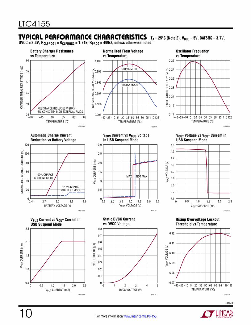
Typical perForMance characTerisTics
Oscillator Frequency vs Temperature
Automatic Charge Current Reduction vs Battery Voltage
VBUS Current vs VBUS Voltage in USB Suspend Mode
VOUT Voltage vs VOUT Current in USB Suspend Mode
VBUS Current vs VOUT Current in USB Suspend Mode
Battery Charger Resistance vs Temperature
Normalized Float Voltage vs Temperature
TA = 25°C (Note 2). VBUS = 5V, BATSNS = 3.7V, DVCC = 3.3V, RCLPROG1 = RCLPROG2 = 1.21k, RPROG = 499Ω, unless otherwise noted.
TEMPERATURE (°C)–40
CHAR
GER
TOTA
L RE
SIST
ANCE
(mΩ
)
50
55
60
60
4613 G10
45
40
35–15 10 35 85
RESISTANCE INCLUDES VISHAYSILICONIX Si5481DU EXTERNAL PMOS
BATTERY VOLTAGE (V)2.4
0
NORM
ALIZ
ED C
HARG
E CU
RREN
T (%
)
20
40
60
80
100
120
2.7 3.0 3.3 3.6
4155 G13
100% CHARGECURRENT MODE
12.5% CHARGECURRENT MODE
VBUS VOLTAGE (V)2.5
0
V BUS
CUR
RENT
(mA)
0.5
1.0
1.5
2.0
3.0
3.0 3.5 4.0 4.5
4155 G14
5.0 5.5
2.5
MAX NOT MAX
VOUT CURRENT (mA)0
V OUT
VOL
TAGE
(V)
3.9
4.0
4.1
1.5 2.5
4155 G15
3.8
3.7
3.60.5 1.0 2.0
4.2
4.3
4.4
VOUT CURRENT (mA)0
V BUS
CUR
RENT
(mA)
1.5
2.0
2.0
4155 G16
1.0
0.50.5 1.0 1.5 2.5
2.5
Static DVCC Current vs DVCC Voltage
Rising Overvoltage Lockout Threshold vs Temperature
TEMPERATURE (°C)–40
0.995
NORM
ALIZ
ED F
LOAT
VOL
TAGE
(V)
0.996
0.998
0.999
1.000
–10 20 35 125
4155 G11
0.997
–25 5 50 65 95 11080
500mA MODE
100mA MODE
TEMPERATURE (°C)
2.17
OSCI
LLAT
OR F
REQU
ENCY
(MHz
)
2.21
2.25
2.29
2.19
2.23
2.27
–10 20 50 80
4155 G12
125110–25–40 5 35 65 95
DVCC VOLTAGE (V)0
DVC
C CU
RREN
T (µ
A)
0.3
0.4
0.5
3 5
4155 G17
0.2
0.1
01 2 4
0.6
0.7
0.8
TEMPERATURE (°C)
6.07
V BUS
VOL
TAGE
(V)
6.09
6.11
6.08
6.10
6.12
–10 20 50 80
4155 G18
125110–25–40 5 35 65 95
LTC4155
114155fd
For more information www.linear.com/LTC4155
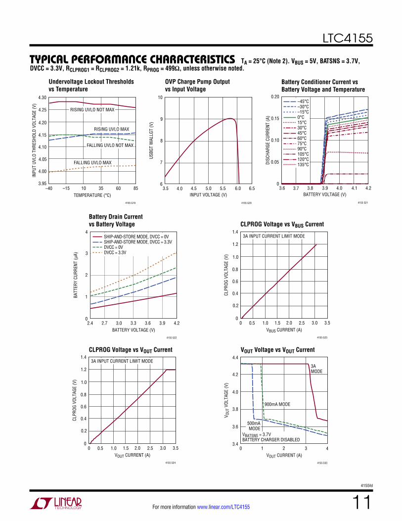
Typical perForMance characTerisTics TA = 25°C (Note 2). VBUS = 5V, BATSNS = 3.7V, DVCC = 3.3V, RCLPROG1 = RCLPROG2 = 1.21k, RPROG = 499Ω, unless otherwise noted.
OVP Charge Pump Output vs Input Voltage
Undervoltage Lockout Thresholds vs Temperature
Battery Conditioner Current vs Battery Voltage and Temperature
Battery Drain Current vs Battery Voltage
TEMPERATURE (°C)–40
4.20
4.25
4.30
60
4155 G19
4.15
4.10
–15 10 35 85
4.05
4.00
3.95
INPU
T UV
LO T
HRES
HOLD
VOL
TAGE
(V)
RISING UVLO MAX
FALLING UVLO MAX
RISING UVLO NOT MAX
FALLING UVLO NOT MAX
INPUT VOLTAGE (V)3.5
6
USBG
T W
ALLG
T (V
)
7
8
9
10
4.0 4.5 5.0 5.5
4155 G20
6.0 6.5BATTERY VOLTAGE (V)
3.60
DISC
HARG
E CU
RREN
T (A
)
0.05
0.10
0.15
0.20
3.7 3.8 3.9 4.0
4155 G21
4.1 4.2
–45°C–30°C–15°C0°C15°C30°C45°C60°C75°C90°C105°C120°C135°C
BATTERY VOLTAGE (V)2.4
BATT
ERY
CURR
ENT
(µA)
2
3
3.6
4155 G22
1
02.7 3.0 3.3 4.23.9
4SHIP-AND-STORE MODE, DVCC = 0VSHIP-AND-STORE MODE, DVCC = 3.3VDVCC = 0VDVCC = 3.3V
CLPROG Voltage vs VBUS Current
CLPROG Voltage vs VOUT Current VOUT Voltage vs VOUT Current
VBUS CURRENT (A)0
0.8
1.0
1.4
1.5 2.5
4155 G23
0.6
0.4
0.5 1.0 2.0 3.0 3.5
0.2
0
1.2
CLPR
OG V
OLTA
GE (V
)
3A INPUT CURRENT LIMIT MODE
VOUT CURRENT (A)0
0.8
1.0
1.4
1.5 2.5
4155 G24
0.6
0.4
0.5 1.0 2.0 3.0 3.5
0.2
0
1.2
CLPR
OG V
OLTA
GE (V
)
3A INPUT CURRENT LIMIT MODE
VOUT CURRENT (A)0
V OUT
VOL
TAGE
(V)
3.8
4.0
4
4155 G33
3.6
3.41 2 3
4.4
3AMODE
4.2
500mAMODE
VBATSNS = 3.7VBATTERY CHARGER DISABLED
900mA MODE
LTC4155
124155fd
For more information www.linear.com/LTC4155
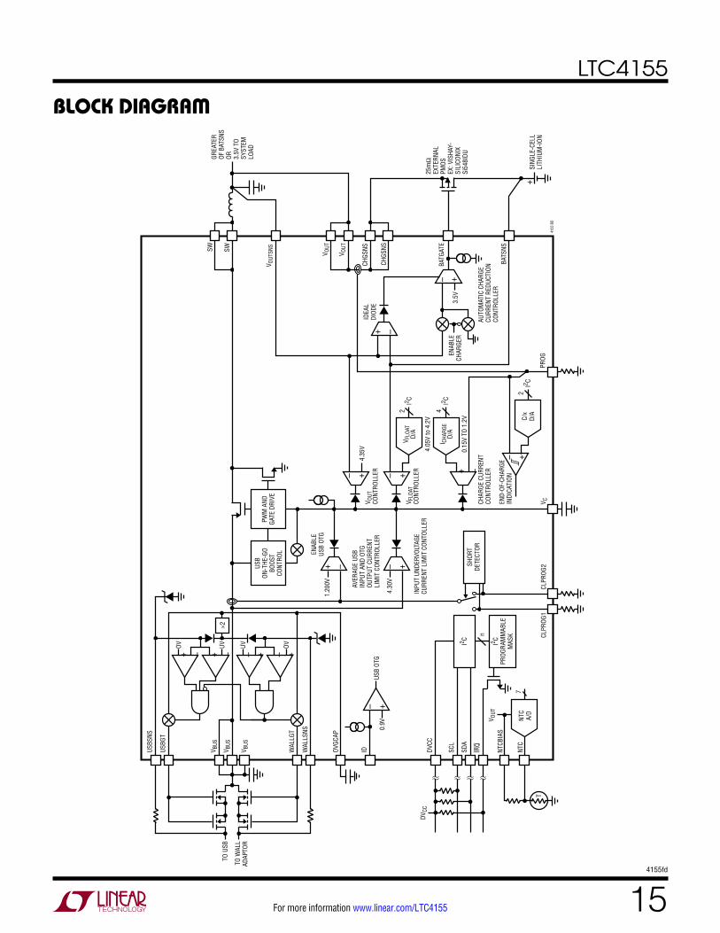
pin FuncTionsSDA (Pin 1): Data Input/Output for the I2C Serial Port. The I2C input levels are scaled with respect to DVCC for I2C compliance.
DVCC (Pin 2): Logic Supply for the I2C Serial Port. DVCC sets the reference level of the SDA and SCL pins for I2C compliance. It should be connected to the same power supply used to power the I2C pull-up resistors.
IRQ (Pin 3): Open-Drain Interrupt Output. The IRQ pin can be used to generate an interrupt due to a variety of maskable status change events within the LTC4155.
ID (Pin 4): USB A-Device Detection Pin. When wired to a mini- or micro-USB connector, the ID pin detects when the “A” side of a mini or micro-USB cable is connected to the product. If the ID pin is pulled down, and the LOCKOUT_ID_PIN bit is not set in the I2C port, the switch-ing PowerPath operates in reverse providing USB power to the VBUS pin from the battery. USB On-The-Go power can only be delivered from the USB multiplexer path.
CLPROG1 (Pin 5): Primary VBUS Current Limit Program-ming Pin. A resistor from CLPROG1 to ground determines the upper limit of the current drawn from the VBUS pin when CLPROG1 is selected. A precise measure of VBUS current, hCLPROG1
–1, is sent to the CLPROG1 pin. The switching regulator increases power delivery until CLPROG1 reaches 1.2V. Therefore, the current drawn from VBUS will be limited to an amount given by the 1.2V reference voltage, hCLPROG1 and RCLPROG1.
Typically CLPROG1 is used to override the USB compliant input current control pin, CLPROG2, in applications where USB compliance is not a requirement. This would be use-ful for applications that use a dedicated wall adapter and would rather not be limited to the 500mW start-up value required by USB specifications. If USB compliance is a requirement at start-up, CLPROG1 should be connected to CLPROG2 and a single resistor should be used. See the CLPROG2 pin description.
In USB noncompliant designs, the user is encouraged to use an RCLPROG1 value that best suits their application for start-up current limit. See the Operation section for more details.
CLPROG2 (Pin 6): Secondary VBUS Current Limit Pro-gram Pin. CLPROG2 controls the VBUS current limit when either selected via I2C command or when CLPROG1 and CLPROG2 are shorted together. When selected, a resistor from CLPROG2 to ground determines the upper limit of the current drawn from the VBUS pin. Like CLPROG1, a precise fraction of VBUS current, hCLPROG2
–1, is sent to the CLPROG2 pin. The switching regulator increases power delivery until CLPROG2 reaches 1.2V. Therefore, the cur-rent drawn from VBUS will be limited to an amount given by the 1.2V reference voltage, hCLPROG2 and RCLPROG2.
There are a multitude of ratios for hCLPROG2 available by I2C control, three of which correspond to the 100mA, 500mA and 900mA USB specifications. CLPROG2 is also used to regulate maximum input current in the USB suspend mode and maximum output current in USB On-The-Go mode.
If CLPROG1 and CLPROG2 are shorted together at the onset of available input power, the LTC4155 selects CLPROG2 in the 100mA USB mode to limit input current. This ensures USB compliance if so desired. For USB compliance in all modes, the user is encouraged to make RCLPROG2 equal to the value declared in the Electrical Characteristics.
WALLSNS (Pin 7): Highest Priority Multiplexer Input and Overvoltage Protection Sense Input. WALLSNS should be connected through a 3.6k resistor to a high priority input power connector and one drain of two source-connected N-channel MOSFET pass transistors. When voltage is detected on WALLSNS, it draws a small amount of current to power a charge pump which then provides gate drive to WALLGT to energize the external transistors. If the input voltage exceeds VOVLO, WALLGT will be pulled to GND to disable the pass transistors and protect the LTC4155 from high voltage.
USBSNS (Pin 8): Lowest Priority Multiplexer Input and Overvoltage Protection Sense Input. USBSNS should be connected through a 3.6k resistor to a low priority input power connector and one drain of two source-connected N-channel MOSFET pass transistors. When voltage is detected on USBSNS, and no voltage is detected on WALLSNS, USBSNS draws a small amount of current to power a charge pump which then provides gate drive to
LTC4155
134155fd
For more information www.linear.com/LTC4155
pin FuncTionsUSBGT to energize the external transistors. If the input voltage exceeds VOVLO, USBGT will be pulled to GND to disable the pass transistors and protect the LTC4155 from high voltage.
Power detected on WALLSNS is prioritized over USBSNS. If power is detected on both WALLSNS and USBSNS, by default, only WALLGT will receive drive for its pass tran-sistors. See the Operations section for further information about programmable priority.
USBGT (Pin 9): Overvoltage Protection and Priority Mul-tiplexer Gate Output. Connect USBGT to the gate pins of two source-connected external N-channel MOSFET pass transistors. One drain of the transistors should be con-nected to VBUS and the other drain should be connected to a low priority DC input connector. In the absence of an overvoltage condition, this pin is driven from an internal charge pump capable of creating sufficient overdrive to fully enhance the pass transistors. If an overvoltage condition is detected, USBGT is brought rapidly to GND to prevent damage to the LTC4155. USBGT works in conjunction with USBSNS to provide this protection. USBGT also works in conjunction with WALLSNS to determine power source prioritization. See the Operation section.
OVGCAP (Pin 10): Overvoltage Protection Capacitor Output. A 0.1µF capacitor should be connected from OVGCAP to GND. OVGCAP is used to store charge so that it can be rapidly moved to WALLGT or USBGT. This feature provides faster power switchover when multiple inputs are supported by the end product.
WALLGT (Pin 11): Overvoltage Protection and Priority Multiplexer Gate Output. Connect WALLGT to the gate pins of two source-connected external N-channel MOSFET pass transistors. One drain of the transistors should be connected to VBUS and the other drain should be connected to a high priority input connector. In the absence of an overvoltage condition, this pin is driven from an internal charge pump capable of creating sufficient gate drive to fully enhance the pass transistors. If an overvoltage condition is detected, WALLGT is brought rapidly to GND to prevent damage to the LTC4155. WALLGT works in conjunction with WALLSNS to provide this protection. WALLGT also works in conjunction with USBSNS to determine power source prioritization. See the Operation section.
VC (Pin 12): Compensation Pin. A 0.047μF ceramic ca-pacitor on this pin compensates the switching regulator control loops.
VOUTSNS (Pin 13): Output Voltage Sense Input. Connecting VOUTSNS directly to the VOUT bypass capacitor ensures that VOUT regulates at the correct level.
NTCBIAS (Pin 14): NTC Thermistor Bias Output. Connect a bias resistor between NTCBIAS and NTC, and a thermistor between NTC and GND. The value of the bias resistor should usually be equal to the nominal value of the thermistor.
NTC (Pin 15): Input to the Negative Temperature Coefficient Thermistor Monitoring Circuit. The NTC pin connects to a negative temperature coefficient thermistor, which is typically copackaged with the battery, to determine if the battery is too warm or too cold to charge or if the battery is dangerously hot. If the battery’s temperature is out of range, charging is paused until the battery temperature re-enters the valid range. A low drift bias resistor is required from NTCBIAS to NTC and a thermistor is required from NTC to ground. The thermistor’s temperature reading is continually digitized by an analog to digital converter and may be read back at any time via the I2C port.
BATSNS (Pin 16): Battery Voltage Sense Input. For proper operation, this pin must always be connected to the battery. For fastest charging, connect BATSNS physically close to the Lithium-Ion cell’s positive terminal. Depending upon available power and load, a Li-Ion battery connected to the BATSNS pin will either be charged from VOUT or will deliver system power to VOUT via the required external P-channel MOSFET transistor.
BATGATE (Pin 17): Battery Charger and Ideal Diode Am-plifier Control Output. This pin controls the gate of an external P-channel MOSFET transistor used to charge the Lithium-Ion cell and to provide power to VOUT when the system load exceeds available input power. The source of the P-channel MOSFET should be connected to CHGSNS and the drain should be connected to BATSNS and the battery.
LTC4155
144155fd
For more information www.linear.com/LTC4155
pin FuncTionsPROG (Pin 18): Charge Current Program and Monitor Pin. A resistor from PROG to GND programs the maximum battery charge rate. The LTC4155 features I2C programmability enabling software selection of fifteen charge currents that are inversely proportional to a single user-supplied programming resistor.
CHGSNS (Pins 19, 20): Battery Charger Current Sense Pin. An internal current sense resistor between VOUT and CHGSNS monitors battery charge current. CHGSNS should be connected to the source of an external P-channel MOSFET transistor.
VOUT (Pins 21, 22): Output Voltage of the Switching PowerPath Controller and Input Voltage of the Battery Charging System. The majority of the portable product should be powered from VOUT. The LTC4155 will partition the available power between the external load on VOUT and the battery charger. Priority is given to the external load and any extra power is used to charge the battery. An ideal diode control function from BATSNS to VOUT ensures that VOUT is powered even if the load exceeds the allotted power from VBUS or if the VBUS power source is removed. VOUT should be bypassed with a low impedance multilayer ceramic capacitor of at least 22µF.
VBUS (Pins 23, 24, 25): Input Voltage for the PowerPath Step-Down Switching Regulator and Output Voltage for the USB On-The-Go Step-Up Switching Regulator. VBUS may be connected to the USB port of a computer or a DC output wall adapter or to one or both optional overvolt-age protection/multiplexer compound transistors. VBUS should be bypassed with a low impedance multilayer ceramic capacitor.
SW (Pins 26, 27): Switching Regulator Power Transmis-sion Pin. The SW pin delivers power from VBUS to VOUT via the step-down switching regulator and from VOUT to VBUS via the step-up switching regulator. A 1μH inductor should be connected from SW to VOUT. See the Applica-tions Information section for a discussion of current rating.
SCL (Pin 28): Clock Input for the I2C Serial Port. The I2C input levels are scaled with respect to DVCC for I2C compliance.
GND (Exposed Pad Pin 29): Exposed pad must be soldered to the PCB to provide a low electrical and thermal imped-ance connection to the printed circuit board’s ground. A continuous ground plane on the second layer of a multilayer printed circuit board is strongly recommended.
LTC4155
154155fd
For more information www.linear.com/LTC4155
block DiagraM
+ – + –
+–
1.20
0V
NTC
CL
PROG
1
CLPR
OG2
PROG
NTCB
IAS
7
T
USBG
T
USBS
NS
×2
4155
BD
SING
LE-C
ELL
LITH
IUM
-ION
25m
Ω
EXTE
RNAL
PM
OSEX
: VIS
HAY-
SILI
CONI
XSi
548I
DU
AVER
AGE
USB
INPU
T AN
D OT
GOU
TPUT
CUR
RENT
LIM
IT C
ONTR
OLLE
R
INPU
T UN
DERV
OLTA
GE
CURR
ENT
LIM
IT C
ONTO
LLER
IDEA
LDI
ODE
ENAB
LECH
ARGE
R
GREA
TER
OF B
ATSN
S OR 3.
5V T
O SY
STEM
LOAD
AUTO
MAT
IC C
HARG
ECU
RREN
T RE
DUCT
ION
CONT
ROLL
ER
OV UV
+–
0.9V
+–
I2 CPR
OGRA
MM
ABLE
MAS
K
I2 C
+
TO W
ALL
ADAP
TOR
TO U
SB
+– +–
ENAB
LEUS
B OT
G
UV OV
V BUS
V BUS
V BUS
WAL
LSNS
WAL
LGT
OVGC
AP
ID
CHGS
NS
CHGS
NS
BATG
ATE
3.5V
BATS
NS
V OUT
V OUT
SNS
V OUT
DVCC
SCL
V OUT
SD
A
IRQ
+ –
USB
OTG
SHOR
TDE
TECT
OR
+ –USB
ON-T
HE-G
OBO
OST
CONT
ROL
PWM
AND
GATE
DRI
VE
V C
4.30
V
+–
+–V O
UTCO
NTRO
LLER
4.35
V
+–
V FLO
ATCO
NTRO
LLER + –
CHAR
GE C
URRE
NTCO
NTRO
LLER
END-
OF-C
HARG
EIN
DICA
TION
SW
SW
DVCC
n
NTC
A/D
I2 C2
V FLO
ATD/
A
4.05
V to
4.2
V
I2 C2
C/x
D/A
I2 C4
I CHA
RGE
D/A
0.15
V TO
1.2
V

LTC4155
164155fd
For more information www.linear.com/LTC4155
TiMing DiagraMs
ACK
1 2 3
WRITE ADDRESS R/W
4 5 6 7 8 9 1 2 3 4 5 6 7 8 9 1 2 3 4 5 6 7 8 9
0 0 0 1 0 0 1 0
0 0 0 1 0 0 1 0 A7 A6 A5 A4 A3 A2 A1 A0 B7 B6 B5 B4 B3 B2 B1 B0
ACK
STOPSTART
SDA
SCL
ACK
SUB ADDRESS INPUT DATA BYTE
OPTIONAL
4155 TD01
I2C Write Protocol
I2C Read Protocol
Timing Diagram
ACK
1 2 3
READ ADDRESS R/W
4 5 6 7 8 9 1 2 3 4 5 6 7 8 9
0 0 0 1 0 0 1 1
0 0 0 1 0 0 1 1 A7 A6 A5 A4 A3 A2 A1 A0
START
SDA
SCL
NACK
OUTPUT DATA BYTE
4155 TD02
tSU, DAT
tHD, STA
tHD, DAT
SDA
SCL
tSU, STAtHD, STA tSU, STO
4155 TD03
tBUFtLOW
tHIGH
STARTCONDITION
(S)
REPEATED STARTCONDITION
(Sr)
STOPCONDITION
(P)
STARTCONDITION
(S)
tr tf
tSP
LTC4155
174155fd
For more information www.linear.com/LTC4155
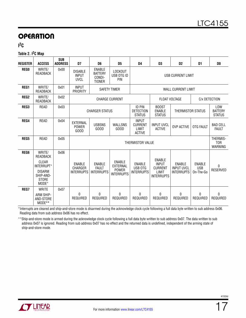
Table 2. I2C Map
REGISTER ACCESSSUB
ADDRESS D7 D6 D5 D4 D3 D2 D1 D0
REG0 WRITE/READBACK
0x00 DISABLE INPUT UVCL
ENABLE BATTERY CONDI-TIONER
LOCKOUT USB OTG ID
PINUSB CURRENT LIMIT
REG1 WRITE/READBACK
0x01 INPUT PRIORITY SAFETY TIMER WALL CURRENT LIMIT
REG2 WRITE/READBACK
0x02 CHARGE CURRENT FLOAT VOLTAGE C/x DETECTION
REG3 READ 0x03CHARGER STATUS
ID PIN DETECTION
STATUS
BOOST ENABLE STATUS
THERMISTOR STATUSLOW
BATTERY STATUS
REG4 READ 0x04 EXTERNAL POWER GOOD
USBSNS GOOD
WALLSNS GOOD
INPUT CURRENT
LIMIT ACTIVE
INPUT UVCL ACTIVE OVP ACTIVE OTG FAULT BAD CELL
FAULT
REG5 READ 0x05THERMISTOR VALUE
THERMIS-TOR
WARNING
REG6 WRITE/READBACK
CLEAR INTERRUPT*
DISARM SHIP-AND-
STORE MODE*
0x06
ENABLE CHARGER
INTERRUPTS
ENABLE FAULT
INTERRUPTS
ENABLE EXTERNAL
POWER INTERRUPTS
ENABLE USB OTG
INTERRUPTS
ENABLE INPUT
CURRENT LIMIT
INTERRUPTS
ENABLE INPUT UVCL INTERRUPTS
ENABLE USB
On-The-Go
0 RESERVED
REG7 WRITEARM SHIP-AND-STORE
MODE**
0x070
REQUIRED0
REQUIRED0
REQUIRED0
REQUIRED0
REQUIRED0
REQUIRED0
REQUIRED0
REQUIRED
*Interrupts are cleared and ship-and-store mode is disarmed during the acknowledge clock cycle following a full data byte written to sub address 0x06. Reading data from sub address 0x06 has no effect.
**Ship-and-store mode is armed during the acknowledge clock cycle following a full data byte written to sub address 0x07. The data written to sub address 0x07 is ignored. Reading from sub address 0x07 has no effect and the returned data is undefined, independent of the arming state of ship-and-store mode.
operaTionI2C
LTC4155
184155fd
For more information www.linear.com/LTC4155
operaTionIntroduction
The LTC4155 is an advanced I2C controlled power man-ager and Li-Ion/Polymer battery charger designed to efficiently transfer up to 15W from a variety of sources while minimizing power dissipation and easing thermal budgeting constraints. By decoupling VOUT and the battery, the innovative instant-on PowerPath architecture ensures that the application is powered immediately after external voltage is applied, even with a completely dead battery, by prioritizing power to the application.
Since VOUT and the battery are decoupled, the LTC4155 includes an ideal diode controller. The ideal diode from the battery to VOUT guarantees that ample power is always available to VOUT even if there is insufficient or absent power at VBUS.
The LTC4155 includes a monolithic step-down switch-ing battery charger for USB support, wall adapters and other 5V sources. By incorporating a unique input current measurement and control system, the switching charger interfaces seamlessly to wall adapters and USB ports without requiring application software to monitor and adjust system loads. Because power is conserved, the LTC4155 allows the load current on VOUT to exceed the current drawn by the USB port or wall adapter, making maximum use of the allowable power for battery charging without exceeding the USB or wall adapter power delivery specifications. A wide range of input current settings as well as battery charge current settings are available for selection by I2C.
Using only one inductor, the switching PowerPath can operate in reverse, boosting the battery voltage to provide 5V power at its input pin for USB On-The-Go applications. In the USB-OTG mode, the switching regulator supports USB high power loads up to 500mA. Protection circuits ensure that the current is limited and ultimately the channel is shut down if a fault is detected on the USB connector.
To support USB low power mode, the LTC4155 can deliver power to the external load and charge the battery through a linear regulator while limiting input current to less than 100mA.
The LTC4155 also features a combination overvoltage protection circuit /priority multiplexer which prevents
damage to its input caused by accidental application of high voltage and selects one of two high power input connectors based on priority.
A thermistor measurement subsystem periodically monitors and reports the battery’s thermistor value via the onboard I2C port. The same circuit then reports when dangerous battery temperatures are reached and can autonomously pause charging and optionally enable a bat-tery safety conditioner. Refer to Overtemperature Battery Conditioner in the Operation section for further details.
To minimize battery drain when a device is connected to a suspended USB port, an LDO from VBUS to VOUT provides the allowable USB suspend current to the application.
An interrupt subsystem can be enabled to alert the host microprocessor of various status change events so that system parameters can be varied as needed by system software. Several status change event categories are maskable for maximum flexibility.
To eliminate battery drain between manufacture and sale, a ship-and-store feature reduces the already low battery standby current to nearly zero and optionally disconnects power from downstream circuitry.
An input undervoltage amplifier optionally prevents the input voltage from decreasing below 4.3V when a resistive cable or current limited supply is providing input power to the LTC4155.
Finally, the LTC4155 has considerable adjustability built in so that power levels and status information can be controlled and monitored via the simple 2-wire I2C port.
Input Current-Limited Step-Down Switching Charger
Power delivery from VBUS to VOUT is controlled by a 2.25MHz constant-frequency step-down switching regu-lator. The switching regulator reduces output power in response to one of six regulation loops, including battery voltage, battery charge current, output voltage, input cur-rent, input undervoltage, and external PMOS charger FET power dissipation. For USB low power (100mA) and USB suspend (2.5mA) modes, the switching regulator is dis-abled and power is transmitted through a linear regulator.
LTC4155
194155fd
For more information www.linear.com/LTC4155
Battery Float Voltage Regulation
When the battery charger is enabled, the switching regula-tor will reduce its output power to prevent VBATSNS from exceeding the programmed battery float voltage, VFLOAT. The float voltage may be selected from among four pos-sible choices via the I2C interface using bits VFLOAT[1:0]. Refer to Table 12.
Battery Charge Current Regulation and Low Cell Trickle Charge
The switching regulator will also reduce its output power to limit battery charge current, ICHARGE, to a programmed maximum value. The battery charge current is programmed using both a resistor, RPROG, between PROG and ground to set default maximum charge current plus I2C adjust-ability to optionally reduce programmed charge current. The battery charge current loop mirrors a precise fraction of the battery charge current, IBAT, to the PROG pin, then reduces switching regulator output power to limit the resultant voltage, VPROG, to one of fifteen possible servo reference voltages.
The following expression may be used to determine the battery charge current at any time by sampling the PROG pin voltage.
IBAT = VPROG
RPROG• 1000
This expression may also be used to calculate the required value of RPROG for any desired charge current. The resis-tor value required to program default maximum charge current may be found by substituting VPROG = 1.200 and solving for RPROG. The other fourteen settings are I2C selectable using ICHARGE[3:0] and reduce the charge current in 6.25% steps. The resulting limits may be found by substituting RPROG and the relevant VPROG servo volt-age from Table 11.
The maximum charge current should be set based on the cell size and maximum charge rate without regard to input current setting or input power source.
The LTC4155 monitors the voltage across the external PMOS transistor and automatically reduces the cur-rent regulation servo voltage at VPROG to limit power
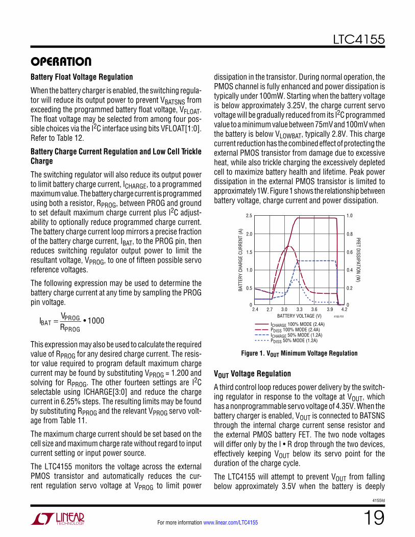
dissipation in the transistor. During normal operation, the PMOS channel is fully enhanced and power dissipation is typically under 100mW. Starting when the battery voltage is below approximately 3.25V, the charge current servo voltage will be gradually reduced from its I2C programmed value to a minimum value between 75mV and 100mV when the battery is below VLOWBAT, typically 2.8V. This charge current reduction has the combined effect of protecting the external PMOS transistor from damage due to excessive heat, while also trickle charging the excessively depleted cell to maximize battery health and lifetime. Peak power dissipation in the external PMOS transistor is limited to approximately 1W. Figure 1 shows the relationship between battery voltage, charge current and power dissipation.
operaTion
Figure 1. VOUT Minimum Voltage Regulation
VOUT Voltage Regulation
A third control loop reduces power delivery by the switch-ing regulator in response to the voltage at VOUT, which has a nonprogrammable servo voltage of 4.35V. When the battery charger is enabled, VOUT is connected to BATSNS through the internal charge current sense resistor and the external PMOS battery FET. The two node voltages will differ only by the I • R drop through the two devices, effectively keeping VOUT below its servo point for the duration of the charge cycle.
The LTC4155 will attempt to prevent VOUT from falling below approximately 3.5V when the battery is deeply
BATTERY VOLTAGE (V)2.4
0
BATT
ERY
CHAR
GE C
URRE
NT (A
)
PFET DISSIPATION (W)
0.5
1.0
1.5
2.0
2.5
0
0.2
0.4
0.6
0.8
1.0
2.7 3.0 3.3 3.64155 F01
3.9 4.2
ICHARGE 100% MODE (2.4A)PDISS 100% MODE (2.4A)ICHARGE 50% MODE (1.2A)PDISS 50% MODE (1.2A)
LTC4155
204155fd
For more information www.linear.com/LTC4155
discharged. This feature allows instant-on operation when the low state of charge would otherwise prevent operation of the system. If the system load plus battery charger load exceeds the available input power, battery charge current will be sacrificed to prioritize the system load and maintain the switching regulator output voltage while continuing to observe the input current limit. If the system load alone exceeds the power available from the input, the output voltage must fall to deliver the additional current, with supplemental current eventually being sup-plied by the battery.
Input Current Regulation
To meet the maximum load specification of the available supply (USB/wall adapter), the switching regulator contains a measurement and control system which ensures that the average input current is below the level programmed at the CLPROG1 or CLPROG2 pin and the I2C port. Con-necting a single 1% tolerance resistor of the recommended value to both the CLPROG1 and CLPROG2 pins guarantees compliance with the 2.5mA, 100mA, 500mA, and 900mA USB 2.0/3.0 current specifications, while also permitting other I2C selectable current limits up to 3A. The input current limit is independently selectable for each of the two inputs, with the USBILIM[4:0] and WALLILIM[4:0] bits in the I2C port. The USB input current limit setting resets to 100mA when power is removed from its respec-tive input. The WALL input current limit setting resets to 100mA when power is removed from both the USB and WALL inputs. Refer to Alternate Default Input Current Limit in the Operation section to program a non USB compli-ant default input current limit for use with wall adapters or other power sources. Refer to Table 8 for a complete listing of I2C programmable input current limit settings.
If the combined external load plus battery charge current is large enough to cause the switching power supply to reach the programmed input current limit, the battery charger will reduce its charge current by precisely the amount necessary to enable the external load to be satisfied. Even if the battery charge current is programmed to exceed the allowable input power, the specification for average input current will not be violated; the battery charger will reduce its current as needed. Furthermore, if the load at VOUT exceeds the programmed power level from VBUS, the
extra load current will be drawn from the battery via the ideal diode independent of whether the battery charger is enabled or disabled.
Input Undervoltage Current Limit
The LTC4155 can tolerate a resistive connection to the input power source by automatically reducing power transmission as the VBUS pin drops to 4.3V preventing a possible UVLO oscillation. The undervoltage current limit feature can be disabled by I2C using the DISABLE_INPUT_UVCL bit. Refer to Table 5.
USB On-The-Go 5V Boost Converter
The LTC4155 switching regulator can be operated in reverse to deliver power from the battery to VBUS while boosting the VBUS voltage to 5V. This mode can be used to implement features such as USB On-The-Go without any additional magnetics or other external components.
The step-up switching regulator may be enabled in one of two ways. The LTC4155 can optionally monitor the ID pin of a USB cable and autonomously start the step-up regulator when a host-side A/B connector is detected with a grounded ID pin. The switching regulator may also be enabled directly with the REQUEST_OTG I2C command. Note that the step-up regulator will not operate if input power is present on either the USB or WALL input, or if the battery voltage is below VLOWBAT, typically 2.8V. The I2C status bits OTG_ENABLED, LOWBAT and OTG_FAULT can be used to determine if the step-up converter is running. Refer to ID Pin Detection in the Operation section for more information about the autonomous step-up regulator start-up.
The step-up regulator only provides power to the USB input. It is not possible to provide power to the WALL input. The I2C PRIORITY setting has no effect on step-up regulator operation. Refer to Dual-Input Overvoltage Protection and Undervoltage Lockout in the Operation section for more information about multiple input operation.
The switching regulator is guaranteed to deliver 500mA to VBUS and will limit its output current to approximately 1.4A while allowing VBUS to fall when overloaded. If a short-circuit fault is detected, the channel will be shut down after approximately 8ms and the problem will be reported with the I2C status bit OTG_FAULT.
operaTion
LTC4155
214155fd
For more information www.linear.com/LTC4155
ID Pin Detection
For USB On-The-Go compatibility, the step-up switching regulator can optionally start autonomously when the grounded ID pin in the A side of an On-The-Go cable is detected.
The ID pin is monitored at all times. Its status is reported in the I2C bit ID_DETECT, reporting true when the ID pin is grounded. Optionally, any change in ID_PIN_DETECT may trigger an interrupt request to notify the system processor. Unless the I2C LOCKOUT_ID_PIN bit has been set, ID pin detection will also automatically start the step-up regulator. Note that LOCKOUT_ID_PIN locks out automatic start-up, but not monitoring of the ID pin. Also, the REQUEST_OTG command may be used to enable the step-up regulator, independent of the state of ID_PIN_DETECT and LOCKOUT_ID_PIN. Note that the regulator will not start if input power is already present on either input. The I2C status bits OTG_ENABLED and OTG_FAULT can be used to determine if the regulator is running.
The ID pin detection circuit will report a short on the ID pin for ID pin impedances lower than approximately 24k. The USB Battery Charging Specification Rev 1.1 added additional signaling to the ID pin, specifying other possible ID pin resistances of RID_A, RID_B and RID_C. These impedances are all larger than the 24k threshold and will typically not cause an ID pin short detection.
Dual-Input Overvoltage Protection and Undervoltage Lockout
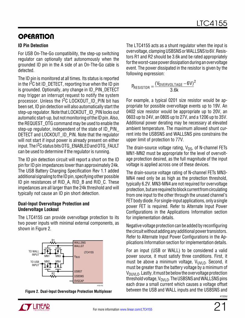
The LTC4155 can provide overvoltage protection to its two power inputs with minimal external components, as shown in Figure 2.
The LTC4155 acts as a shunt regulator when the input is overvoltage, clamping USBSNS or WALLSNS to 6V. Resis-tors R1 and R2 should be 3.6k and be rated appropriately for the worst-case power dissipation during an overvoltage event. The power dissipated in the resistor is given by the following expression:
PRESISTOR = (VOVERVOLTAGE − 6V)
3.6k
2
For example, a typical 0201 size resistor would be ap-propriate for possible overvoltage events up to 19V. An 0402 size resistor would be appropriate up to 20V, an 0603 up to 24V, an 0805 up to 27V, and a 1206 up to 35V. Additional power derating may be necessary at elevated ambient temperature. The maximum allowed shunt cur-rent into the USBSNS and WALLSNS pins constrains the upper limit of protection to 77V.
The drain-source voltage rating, VDS, of N-channel FETs MN1-MN2 must be appropriate for the level of overvolt-age protection desired, as the full magnitude of the input voltage is applied across one of these devices.
The drain-source voltage rating of N-channel FETs MN3-MN4 need only be as high as the protection threshold, typically 6.2V. MN3-MN4 are not required for overvoltage protection, but are required to block current from circulating from one input to the other through the unused channel’s FET body diode. For single-input applications, only a single power FET is required. Refer to Alternate Input Power Configurations in the Applications Information section for implementation details.
Negative voltage protection can be added by reconfiguring the circuit without adding any additional power transistors. Refer to Alternate Input Power Configurations in the Ap-plications Information section for implementation details.
For an input (USB or WALL) to be considered a valid power source, it must satisfy three conditions. First, it must be above a minimum voltage, VUVLO. Second, it must be greater than the battery voltage by a minimum of VDUVLO. Lastly, it must be below the overvoltage protection threshold voltage, VOVLO. The USBSNS and WALLSNS pins each draw a small current which causes a voltage offset between the USB and WALL inputs and the USBSNS and Figure 2. Dual-Input Overvoltage Protection Multiplexer
VBUS
TO USBINPUT
TO WALLINPUT
OVGCAP
USBGT
USBSNS
WALLGT
LTC4155
WALLSNS
4155 F02
MN1
R1
R2
MN3
MN2 MN4
operaTion
LTC4155
224155fd
For more information www.linear.com/LTC4155
WALLSNS pins. The voltage threshold values previously listed and specified in the Electrical Characteristics table are valid when each input is connected to its respective sense pin through a 3.6k resistor.
The status of the USB and WALL inputs is monitored continuously and reported by I2C, with the option of generating several interrupts. When all three conditions previously listed are true, the LTC4155 will report the input valid by asserting USBSNSGD or WALLSNSGD in the I2C port. Optionally, if external power interrupts are enabled, an interrupt request will be generated.
When power is applied simultaneously to both inputs, the LTC4155 will draw power from the WALL input by default. If the I2C PRIORITY bit is asserted, the LTC4155 will instead draw power from the USB input when both inputs are present. The USB On-The-Go step-up regulator delivers power only to the USB input, and the PRIOR-ITY bit is ignored in this mode. The input current limits USBILIM[4:0] and WALLILIM[4:0] also reset to 100mA default mode under different criteria. In all other respects, the two inputs are identical.
An optional capacitor may be placed between the OVGCAP pin and GND to minimize input current disruption when switching from one input to the other while operating at high power levels. The capacitor must be rated to withstand at least 13V and should be approximately ten times larger than the total gate capacitance of the series NMOS power transistors. Capacitance on this pin can also be used to slow the gate charging if the application requires controlled inrush current to any additional input capacitance on the VBUS pin. If fast switching between input or inrush control is not necessary, OVGCAP may be left unconnected.
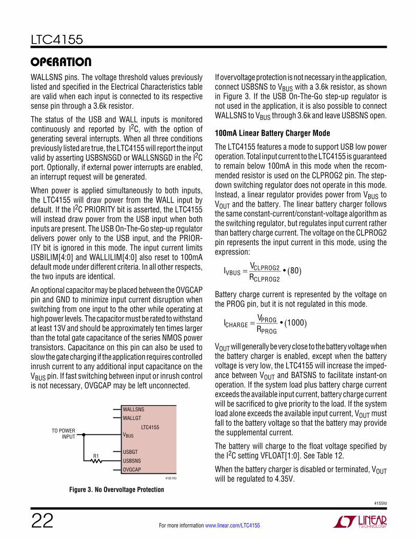
If overvoltage protection is not necessary in the application, connect USBSNS to VBUS with a 3.6k resistor, as shown in Figure 3. If the USB On-The-Go step-up regulator is not used in the application, it is also possible to connect WALLSNS to VBUS through 3.6k and leave USBSNS open.
100mA Linear Battery Charger Mode
The LTC4155 features a mode to support USB low power operation. Total input current to the LTC4155 is guaranteed to remain below 100mA in this mode when the recom-mended resistor is used on the CLPROG2 pin. The step-down switching regulator does not operate in this mode. Instead, a linear regulator provides power from VBUS to VOUT and the battery. The linear battery charger follows the same constant-current/constant-voltage algorithm as the switching regulator, but regulates input current rather than battery charge current. The voltage on the CLPROG2 pin represents the input current in this mode, using the expression:
IVBUS = VCLPROG2
RCLPROG2• 80( )
Battery charge current is represented by the voltage on the PROG pin, but it is not regulated in this mode.
ICHARGE = VPROG
RPROG• 1000( )
VOUT will generally be very close to the battery voltage when the battery charger is enabled, except when the battery voltage is very low, the LTC4155 will increase the imped-ance between VOUT and BATSNS to facilitate instant-on operation. If the system load plus battery charge current exceeds the available input current, battery charge current will be sacrificed to give priority to the load. If the system load alone exceeds the available input current, VOUT must fall to the battery voltage so that the battery may provide the supplemental current.
The battery will charge to the float voltage specified by the I2C setting VFLOAT[1:0]. See Table 12.
When the battery charger is disabled or terminated, VOUT will be regulated to 4.35V.
operaTion
VBUSTO POWER
INPUT
OVGCAP
USBGT
USBSNS
WALLGT
LTC4155
WALLSNS
4155 F03
R1
Figure 3. No Overvoltage Protection
LTC4155
234155fd
For more information www.linear.com/LTC4155
2.5mA Linear Suspend Mode
The LTC4155 can supply a small amount of current from VBUS to VOUT to power the system and reduce battery discharge when the product has access to a suspended USB port. When the system load current is less than the current available from the suspended USB port, the volt-age at VOUT will be regulated to 4.35V. If the system load current exceeds USB input current limit, the voltage at VOUT will fall to the battery voltage and any supplemental current above that available from the USB port will be supplied by the battery. CLPROG2 will servo to 103mV in current limit. Battery charging is disabled in suspend mode. Either the USB or WALL input may utilize this current limited suspend mode by programming the appropriate setting in the respective USBILIM or WALLILIM register.
Ideal Diode and Minimum VOUT Controller
The LTC4155 features an ideal diode controller to ensure that the system is provided with sufficient power even when input power is absent or insufficient. This requires an external PMOS transistor with its source connected to CHGSNS, gate to BATGATE, and drain to BATSNS. The controller modulates the gate voltage of the PMOS tran-sistor to allow current to flow from the battery to VOUT to power the system while blocking current in the opposite direction to prevent overcharging of the battery.
The ideal diode controller has several modes of operation. When input power is available and the battery is charging, the PMOS gate will generally be grounded to maximize conduction between the switching regulator and the battery for maximum efficiency. If the battery is deeply discharged, the LTC4155 will automatically increase the impedance between the switching regulator and the battery enough to prevent VOUT from falling below approximately 3.5V. Power to the system load is always prioritized over battery charge current. Increasing the impedance between VOUT and the battery does not necessarily affect the battery charge current, but it may do so for one of the following two reasons:
1. The charge current will be limited to prevent excessive power dissipation in the external PMOS as it becomes more resistive. Charge current reduction begins when the voltage across the PMOS reaches approximately 250mV, and can reduce the charge current as low as 8% full scale. Maximum power dissipation in the PMOS is limited to approximately 1W with RPROG = 499Ω.
2. When limited power is available to the switching regula-tor because either the programmed input current limit or input undervoltage current limit is active, charge current will automatically be reduced to prioritize power delivery to the system at VOUT. VOUT will be maintained at 3.5V as long as possible without exceed-ing the input power limitation. If the system load alone requires more power than is available from the input after charge current has been reduced to zero, VOUT must fall to the battery voltage as the battery begins providing supplemental power.
When input power is available, but the battery charger is disabled or charging has terminated, VOUT and the bat-tery are normally disconnected to prevent overcharging the battery. If the power required by the system should exceed the power available from the input, either because of input current limit or input undervoltage current limit, VOUT will fall to the battery voltage and any additional cur-rent required by the load will be supplied by the battery through the ideal diode.
When input power is unavailable, the ideal diode switches to a low power mode which maximizes conduction and power transmission efficiency between VOUT and the bat-tery by grounding the PMOS gate.
Finally, when ship-and-store mode is activated, the ideal diode is shut down and BATGATE is driven to the battery voltage to prevent conduction through the PMOS. Note that with a single FET, conduction to VOUT is still possible through the body connection diode. Refer to Low Power Ship-and-Store Mode in the Operation section for more information about this mode.
operaTion
LTC4155
244155fd
For more information www.linear.com/LTC4155
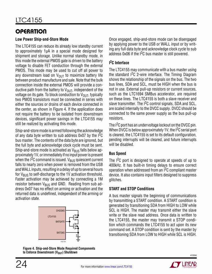
Figure 4. Ship-and-Store Mode Required Components to Enforce Downstream (VOUT) Shutdown
CHGSNS
BATSNS
BATGATE
LTC4155
4155 F04
+
Low Power Ship-and-Store Mode
The LTC4155 can reduce its already low standby current to approximately 1µA in a special mode designed for shipment and storage. Unlike normal standby mode, in this mode the external PMOS gate is driven to the battery voltage to disable FET conduction through the external PMOS. This mode may be used to cut off all power to any downstream load on VOUT to maximize battery life between product manufacture and sale. Note that the bulk connection inside the external PMOS will provide a con-ductive path from the battery to VOUT, independent of the voltage on its gate. To block conduction to VOUT, typically two PMOS transistors must be connected in series with either the sources or drains of each device connected in the center, as shown in Figure 4. If the application does not require the battery to be isolated from downstream devices, significant power savings in the LTC4155 may still be realized by activating this mode.
Ship-and-store mode is armed following the acknowledge of any data byte written to sub address 0x07 by the I2C bus master. The contents of the data byte are ignored, but the full byte and acknowledge clock cycle must be sent. Ship-and-store mode is activated as VBUS falls below ap-proximately 1V, or immediately if no input power is present when the I2C command is issued. VBUS quiescent current falls to nearly zero when power is removed from the USB and WALL inputs, resulting in a delay of up to several hours for VBUS to self-discharge to the 1V activation threshold. Faster activation may be achieved by connecting a 1M resistor between VBUS and GND. Reading from sub ad-dress 0x07 has no effect on arming or activation and the returned data is undefined, independent of the arming or activation state.
Once engaged, ship-and-store mode can be disengaged by applying power to the USB or WALL input or by writ-ing any full data byte and acknowledge clock cycle to sub address 0x06 if the I2C bus master is still powered.
I2C Interface
The LTC4155 may communicate with a bus master using the standard I2C 2-wire interface. The Timing Diagram shows the relationship of the signals on the bus. The two bus lines, SDA and SCL, must be HIGH when the bus is not in use. External pull-up resistors or current sources, such as the LTC1694 SMBus accelerator, are required on these lines. The LTC4155 is both a slave receiver and slave transmitter. The I2C control signals, SDA and SCL, are scaled internally to the DVCC supply. DVCC should be connected to the same power supply as the bus pull-up resistors.
The I2C port has an undervoltage lockout on the DVCC pin. When DVCC is below approximately 1V, the I2C serial port is cleared, the LTC4155 is set to its default configuration, pending interrupts will be cleared, and future interrupts will be disabled.
Bus Speed
The I2C port is designed to operate at speeds of up to 400kHz. It has built-in timing delays to ensure correct operation when addressed from an I2C compliant master device. It also contains input filters designed to suppress glitches.
START and STOP Conditions
A bus master signals the beginning of communications by transmitting a START condition. A START condition is generated by transitioning SDA from HIGH to LOW while SCL is HIGH. The master may transmit either the slave write or the slave read address. Once data is written to the LTC4155, the master may transmit a STOP condi-tion which commands the LTC4155 to act upon its new command set. A STOP condition is sent by the master by transitioning SDA from LOW to HIGH while SCL is HIGH.
operaTion
LTC4155
254155fd
For more information www.linear.com/LTC4155
Byte Format
Each frame sent to or received from the LTC4155 must be eight bits long, followed by an extra clock cycle for the acknowledge bit. The data should be sent to the LTC4155 most significant bit (MSB) first.
Master and Slave Transmitters and Receivers
Devices connected to an I2C bus may be classified as either master or slave. A typical bus is composed of one or more master devices and a number of slave devices. Some devices are capable of acting as either a master or a slave, but they may not change roles while a transaction is in progress.
The transmitter/receiver relationship is distinct from that of master and slave. The transmitter is responsible for control of the SDA line during the eight bit data portion of each frame. The receiver is responsible for control of SDA during the ninth and final acknowledge clock cycle of each frame.
All transactions are initiated by the master with a START or repeat START condition. The master controls the active (falling) edge of each clock pulse on SCL, regardless of its status as transmitter or receiver. The slave device never brings SCL LOW, but may extend the SCL LOW time to implement clock stretching if necessary. The LTC4155 does not clock stretch and will never hold SCL LOW under any circumstance.
The master device begins each I2C transaction as the transmitter and the slave device begins each transaction as the receiver. For bus write operations, the master acts as the transmitter and the slave acts as receiver for the duration of the transaction. For bus read operations, the master and slave exchange transmit/receive roles following the address frame for the remainder of the transaction.
Acknowledge
The acknowledge signal (ACK) is used for handshaking between the transmitter and receiver. When the LTC4155 is written to, it acknowledges its write address as well as the subsequent data bytes as a slave receiver. When it is read from, the LTC4155 acknowledges its read address
as a slave receiver. The LTC4155 then changes to a slave transmitter and the master receiver may optionally acknowl-edge receipt of the following data byte from the LTC4155.
The acknowledge related clock pulse is always generated by the bus master. The transmitter (master or slave) releases the SDA line (HIGH) during the acknowledge clock cycle. The receiver (slave or master) pulls down the SDA line during the acknowledge clock pulse so that it is a stable LOW during the HIGH period of this clock pulse.
When the LTC4155 is read from, it releases the SDA line after the eighth data bit so that the master may acknowl-edge receipt of the data. The I2C specification calls for a not acknowledge (NACK) by the master receiver following the last data byte during a read transaction. Upon receipt of the NACK, the slave transmitter is instructed to release control of the bus. Because the LTC4155 only transmits one byte of data under any circumstance, a master ac-knowledging or not acknowledging the data sent by the LTC4155 has no consequence. The LTC4155 will release the bus in either case.
Slave Address
The LTC4155 responds to a 7-bit address which has been factory programmed to 0b0001_001[R/W]. The LSB of the address byte, known as the read/write bit, should be 0 when writing data to the LTC4155, and 1 when reading data from it. Considering the address an 8-bit word, then the write address is 0x12, and the read address is 0x13. The LTC4155 will acknowledge both its read and write addresses.
Sub Addressed Access
The LTC4155 has four command registers for control input and three status registers for status reporting. They are accessed by the I2C port via a sub addressed pointer system where each sub address value points to one of the seven control or status registers within the LTC4155. The sub address pointer is always the first byte written immediately following the LTC4155 write address dur-ing bus write operations. The sub address pointer value persists after the bus write operation and will determine which data byte is returned by the LTC4155 during any
operaTion
LTC4155
264155fd
For more information www.linear.com/LTC4155
subsequent bus read operations. The sub address pointer register is equivalent to the command code byte within the SMBus write byte and read byte protocols explained in detail under the SMBus Protocol Compatibility section.
Bus Write Operation
The bus master initiates communication with the LTC4155 with a START condition and the LTC4155’s write address. If the address matches that of the LTC4155, the LTC4155 returns an acknowledge. The bus master should then deliver the sub address. The sub address value is transferred to a special pointer register within the LTC4155 upon the return of the sub address acknowledge bit by the LTC4155. If the master wishes to continue the write transaction, it may then deliver the data byte. The data byte is transferred to an internal pending data register at the location of the sub address pointer when the LTC4155 acknowledges the data byte. The LTC4155 is then ready to receive a new sub address, optionally repeating the [SUB ADDRESS][DATA] cycle indefinitely. After the write address, the odd position bytes always represent a sub address pointer assignment and the even position bytes always represent data to be stored at the location referenced by the sub address pointer. The master may terminate communication with the LTC4155 after any even or odd number of bytes with either a repeat START or a STOP condition. If a repeat START condition is initiated by the master, the LTC4155, or any other chip on the I2C bus, can then be addressed. The LTC4155 will remember, but not act on, the last input of valid data that it received at each sub address location. This cycle can also continue indefinitely. Once all chips on the bus have been addressed and sent valid data, a global STOP can be sent and the LTC4155 will immediately update all of its command registers with the most recent pending data that it had previously received. This delayed execution behavior is compliant with the PMBus group command protocol.
Bus Read Operation
The LTC4155 contains seven readable registers. Three are read only and contain status information. Four contain control information which may be both written and read back by the bus master.
Only one of the seven sub addressed data registers is ac-cessible during each bus read operation. The data returned by the LTC4155 is from the data register pointed to by the contents of the sub address pointer register. The pointer register contents are determined by the most recent previ-ous bus write operation.
In preparation for a bus read operation, it may be ad-vantageous for a bus master to prematurely terminate a write transaction with a STOP or repeat START condition after transmitting only an odd number of bytes. The last transmitted byte then represents a pointer to the register of interest for the subsequent bus read operation.
The bus master reads status data from the LTC4155 with a START or repeat START condition followed by the LTC4155 read address. If the read address matches that of the LTC4155, the LTC4155 returns an acknowledge. Following the acknowledgement of its read address, the LTC4155 returns one bit of status information for each of the next eight clock cycles from the register selected by the sub address pointer. Additional clock cycles from the master after the single data byte has been read will leave the SDA line high (0xFF transmitted). The LTC4155 will never acknowledge any bytes during a bus read operation with the exception of its read address.
To read the same register again, the transaction may be repeated starting with a START followed by the LTC4155 read address. It is not necessary to rewrite the sub address pointer register if the sub address has not changed. To read a different register, a write transaction must be initiated with a START or repeat START followed by the LTC4155 write address and sub address pointer byte before the read transaction may be repeated.
When the contents of the sub address pointer register point to a writeable command register, the data returned in a bus read operation is the pending command data at that location if it had been modified since the last STOP condition. After a STOP condition, all pending data is copied to the command registers for immediate effect. The contents of several writeable registers within the LTC4155 are modified upon removal of input power without an I2C transaction. USBILIM[4:0] and WALLILIM[4:0] default to either 100mA mode (0x00) or CLPROG1 mode (0x1F)
operaTion
LTC4155
274155fd
For more information www.linear.com/LTC4155
as explained in the Alternate Default Input Current Limit section of Operation. Thus, the contents of these registers may be different from the last value written by the bus master, and reading back the contents may be useful to determine the state of the system.
When the contents of the sub address pointer register point to a read-only status register, the data returned is a snapshot of the state of the LTC4155 at a particular instant in time. If no interrupt requests are pending, the status data is sampled when the LTC4155 acknowledges its read address, just before the LTC4155 begins data transmis-sion during a bus read operation. When an unmasked interrupt event takes place, the IRQ pin is driven low and data is latched in the three read-only status registers at that moment. Any subsequent read operation from any status registers will return this frozen data to facilitate determination of the cause of the interrupt request. After the bus master clears the LTC4155 interrupt request, the status latches are cleared. Bus read operations will then again return either a snapshot of the data at the read ad-dress acknowledge, or at the time of the next interrupt assertion, whichever comes first.
SMBus Protocol Compatibility
The SMBus specification is generally compatible with the I2C bus specification, but extends beyond I2C to define and standardize specific protocol formats for various types of transactions. The LTC4155 I2C interface is fully compatible with four of the protocols defined by the SMBus speci-fication. All control and status features of the LTC4155 can be accessed using the SMBus protocols, although if high bus utilization is a concern, certain operations can be accomplished more efficiently by I2C bus operations that do not adhere to any of the SMBus defined protocols.
SMBus Write Byte Protocol
1 7 1 1 8 1 8 1 1
S SLAVE ADDRESS
WR A COMMAND CODE
A DATA BYTE A P
The SMBus write byte protocol can be used to modify the contents of any single control register in the LTC4155. The transaction is initiated by the bus master with a START condition. The SMBus slave address corresponds to the
LTC4155 write address, which is 0x09 when interpreted as a 7-bit word (0b 000 1001), followed by WR (value 0b0). The LTC4155 will acknowledge its write address. The SMBus command code corresponds to the sub address pointer value and will be written to the sub address pointer register in the LTC4155. Only the register locations with write access (0x00 to 0x02, 0x06 to 0x07) are meaningful values for the sub address pointer when using this protocol. The LTC4155 will acknowledge the SMBus command code byte. The SMBus data byte corresponds to the command data to be written to the location pointed to by the sub address pointer register. The LTC4155 will acknowledge the SMBus data byte. The STOP condition at the end of the sequence will force an update to the command registers, causing the new command data to take immediate effect.
SMBus Read Byte Protocol
1 7 1 1 8 1 1 7 1 1 8 1 1
S SLAVE ADDRESS
WR A COMMAND CODE
A Sr SLAVE ADDRESS
RD A DATA BYTE
A P
The SMBus read byte protocol can be used to read the contents of any one of the seven control or status regis-ters with one bus transaction. The transaction is initiated by the bus master with a START condition. The SMBus slave address corresponds to the LTC4155 write address, which is 0x09 when interpreted as a 7-bit word (0b 000 1001), followed by WR (value 0b0). The LTC4155 will acknowledge its write address. The SMBus command code corresponds to the sub address pointer value and will be written to the sub address pointer register in the LTC4155. The LTC4155 will acknowledge the SMBus command code byte. The master then issues a repeat START condition, followed by the LTC4155 slave address (0x09) and RD (0b1). The LTC4155 will acknowledge its read address. At this time the bus master becomes a receiver while continuing to clock SCL. The LTC4155 becomes a slave transmitter and controls SDA to place data on the bus. Following the single data byte, the bus master has the option of transmitting either an ACK or a NACK bit. According to the I2C specification, a master must transmit a NACK at the end of a read transaction to instruct the slave to terminate data transmission. Because the LTC4155 terminates data transmission after one byte in all cases, whether the bus master transmits an ACK or
operaTion
LTC4155
284155fd
For more information www.linear.com/LTC4155
a NACK is irrelevant. Finally, a STOP condition returns the bus to the idle state.
SMBus Send Byte Protocol
1 7 1 1 8 1 1
S SLAVE ADDRESS WR A DATA BYTE A P
The SMBus send byte protocol can be used to modify the contents of the sub address pointer register without modifying the contents of any control registers. It has util-ity when preparing to later read status information from the LTC4155 using the SMBus receive byte protocol. The transaction is initiated by the bus master with a START condition. The SMBus slave address corresponds to the LTC4155 write address, which is 0x09 when interpreted as a 7-bit word (0b 000 1001) followed by WR (value 0b0). The LTC4155 will acknowledge its write address. The SMBus data byte corresponds to the sub address pointer value and will be written to the sub address pointer register in the LTC4155. Note that the data byte in this protocol is analogous to the command code in the write byte and read byte protocols. The LTC4155 will acknowledge the SMBus data byte. Finally, a STOP condition returns the bus to the idle state.
SMBus Receive Byte Protocol
1 7 1 1 8 1 1
S SLAVE ADDRESS RD A DATA BYTE A P
The SMBus receive byte protocol can be used to read the contents of the command or status register already selected by the sub address pointer register. This protocol is incapable of modifying the contents of the sub address pointer register, but may be useful to poll a single status register repeatedly with much less bus overhead than the other SMBus protocols. The sub address pointer register can be modified by any of the SMBus write byte, read byte or send byte protocols and the register contents will persist until they are modified again by one of these three protocols.
The receive byte transaction is initiated by the bus master with a START condition. The SMBus slave address corre-
sponds to the LTC4155 read address, which is 0x09 when interpreted as a 7-bit word (0b 000 1001), followed by RD (value 0b1). The LTC4155 will acknowledge its read address. At this time the bus master becomes a receiver while continuing to clock SCL. The LTC4155 becomes a slave transmitter and controls SDA to place data on the bus. Following the single data byte, the bus master has the option of transmitting either an ACK or a NACK bit. According to the I2C specification, a master must trans-mit a NACK at the end of a read transaction to instruct the slave to terminate data transmission. Because the LTC4155 terminates data transmission after one byte in all cases, whether the bus master transmits an ACK or a NACK is irrelevant. Finally, a STOP condition returns the bus to the idle state.
Programmable Interrupt Controller
The LTC4155 can optionally generate active LOW, level-triggered interrupt requests on the IRQ pin in response to a number of status change or fault events. The three available bytes of status information are also frozen at the time the interrupt is triggered to aid in determining the cause of a transient interrupt. The contents of the four writeable command registers are never frozen by interrupts. The interrupt trigger events are grouped into six individually maskable categories corresponding to battery charger status, faults, input power detection, USB On-The-Go, input current limit and input undervoltage cur-rent limit. The interrupt mask register (IMR) is located at sub address location 0x06, with the six most significant bits representing the mask programming. Refer to Table 3. Table 4 lists the status triggers for each interrupt category. Upon power-up, all interrupts default to disabled (masked). Each interrupt category may be enabled by writing a “1” to the appropriate position in the IMR. Any data written to sub address 0x06 also has the side effect of clearing the pending interrupt upon the acknowledge bit of the data (third) byte. Clearing the interrupt releases the IRQ pin and resumes status reporting of live data until the next interrupt. If no change to the interrupt mask is desired, the bus master must rewrite the previous data to sub address 0x06 to clear an interrupt request.
operaTion
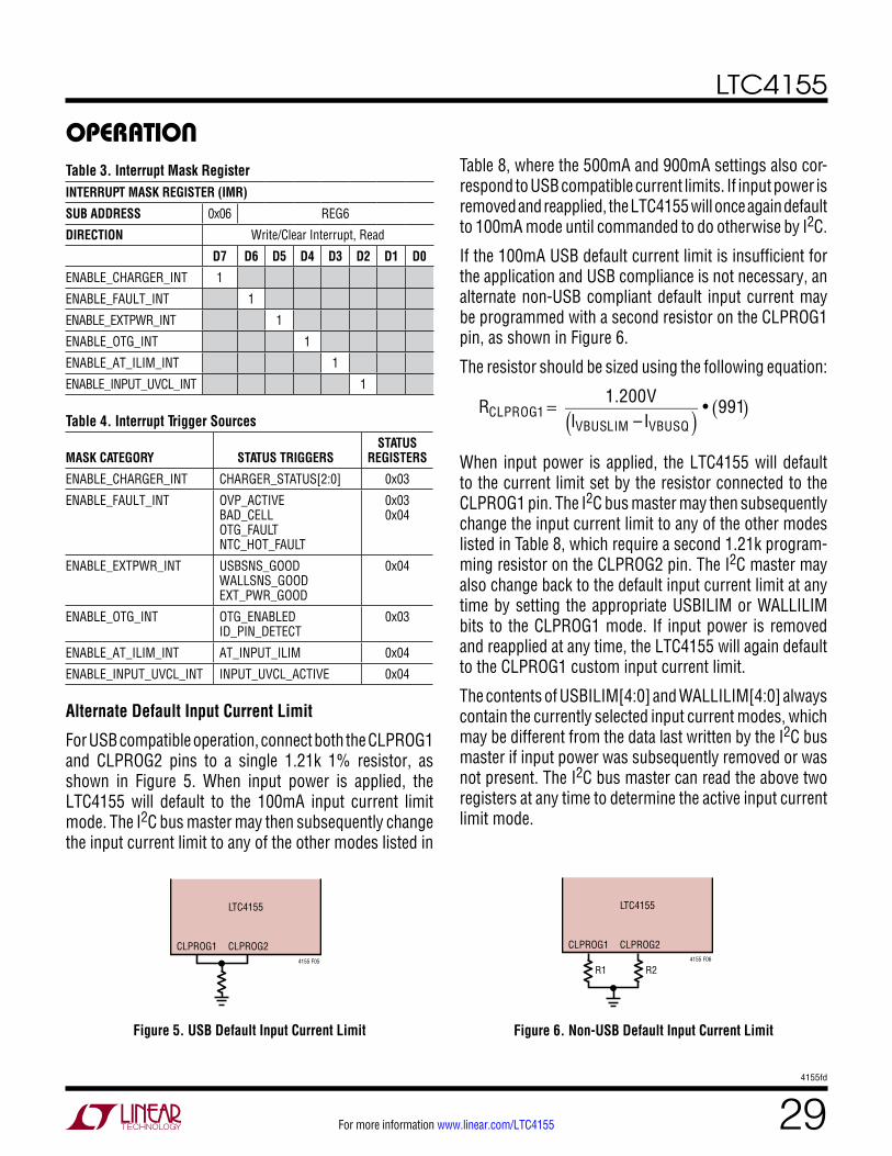
LTC4155
294155fd
For more information www.linear.com/LTC4155
Table 3. Interrupt Mask RegisterINTERRUPT MASK REGISTER (IMR)
SUB ADDRESS 0x06 REG6
DIRECTION Write/Clear Interrupt, Read
D7 D6 D5 D4 D3 D2 D1 D0
ENABLE_CHARGER_INT 1
ENABLE_FAULT_INT 1
ENABLE_EXTPWR_INT 1
ENABLE_OTG_INT 1
ENABLE_AT_ILIM_INT 1
ENABLE_INPUT_UVCL_INT 1
Table 4. Interrupt Trigger Sources
MASK CATEGORY STATUS TRIGGERSSTATUS
REGISTERS
ENABLE_CHARGER_INT CHARGER_STATUS[2:0] 0x03
ENABLE_FAULT_INT OVP_ACTIVE BAD_CELL OTG_FAULT NTC_HOT_FAULT
0x03 0x04
ENABLE_EXTPWR_INT USBSNS_GOOD WALLSNS_GOOD EXT_PWR_GOOD
0x04
ENABLE_OTG_INT OTG_ENABLED ID_PIN_DETECT
0x03
ENABLE_AT_ILIM_INT AT_INPUT_ILIM 0x04
ENABLE_INPUT_UVCL_INT INPUT_UVCL_ACTIVE 0x04
Alternate Default Input Current Limit
For USB compatible operation, connect both the CLPROG1 and CLPROG2 pins to a single 1.21k 1% resistor, as shown in Figure 5. When input power is applied, the LTC4155 will default to the 100mA input current limit mode. The I2C bus master may then subsequently change the input current limit to any of the other modes listed in
Table 8, where the 500mA and 900mA settings also cor-respond to USB compatible current limits. If input power is removed and reapplied, the LTC4155 will once again default to 100mA mode until commanded to do otherwise by I2C.
If the 100mA USB default current limit is insufficient for the application and USB compliance is not necessary, an alternate non-USB compliant default input current may be programmed with a second resistor on the CLPROG1 pin, as shown in Figure 6.
The resistor should be sized using the following equation:
RCLPROG1 = 1.200V
IVBUSLIM – IVBUSQ( ) • 991( )
When input power is applied, the LTC4155 will default to the current limit set by the resistor connected to the CLPROG1 pin. The I2C bus master may then subsequently change the input current limit to any of the other modes listed in Table 8, which require a second 1.21k program-ming resistor on the CLPROG2 pin. The I2C master may also change back to the default input current limit at any time by setting the appropriate USBILIM or WALLILIM bits to the CLPROG1 mode. If input power is removed and reapplied at any time, the LTC4155 will again default to the CLPROG1 custom input current limit.
The contents of USBILIM[4:0] and WALLILIM[4:0] always contain the currently selected input current modes, which may be different from the data last written by the I2C bus master if input power was subsequently removed or was not present. The I2C bus master can read the above two registers at any time to determine the active input current limit mode.
CLPROG2CLPROG1
LTC4155
4155 F05
Figure 5. USB Default Input Current Limit
operaTion
CLPROG2CLPROG1
R2R1
LTC4155
4155 F06
Figure 6. Non-USB Default Input Current Limit
LTC4155
304155fd
For more information www.linear.com/LTC4155
Battery Charger Operation
The LTC4155 contains a fully featured constant-current/constant-voltage Li-Ion/Li-Polymer battery charger with automatic recharge, bad cell detection, trickle charge, programmable safety timer, thermistor temperature qualified charging, programmable end-of-charge indica-tion, programmable float voltage, programmable charge current, detailed I2C status reporting, and programmable interrupt generation.
Precharge/Low Battery
When a battery charge cycle begins, the battery charger first determines if the battery is deeply discharged. If the battery voltage is below VTRKL, typically 2.8V, the LTC4155 will report the LOWBAT condition via I2C (see Table 18). If the low battery voltage persists for more than one-half hour, the battery charger automatically terminates and indicates via the I2C port that the battery was unrespon-sive. When the battery voltage is low, charge current is reduced, both to protect the battery and to prevent exces-sive power dissipation in the external PMOS transistor. Figure 1 shows the relationship between battery voltage and charge current reduction. When input power (USB or WALL) is unavailable, the I2C LOWBAT indication will always be true, independent of the actual state of charge of the battery and can be disregarded.
Constant-Current
When the battery voltage is above approximately 3.3V, the charger will attempt to deliver the programmed charge cur-rent in constant-current mode. Depending on available input power and external load conditions, the battery charger may or may not be able to charge at the full programmed rate. The external load will always be prioritized over the battery charge current. Likewise, the USB and WALL input current limit programming will always be observed and only additional power will be available to charge the bat-tery. When system loads are light, battery charge current will be maximized.
The upper limit of charge current is programmed by the combination of a resistor from PROG to ground and the PROG servo voltage value set in the I2C port. The maximum charge current will be given by the following expression:
ICHARGE = VPROG
RPROG• 1000
VPROG can be set by the I2C port and ranges from 150mV to 1.2V in 75mV steps. The default value of VPROG is 1.2V. VPROG is controlled by bits ICHARGE[3:0] located at sub address 0x02. See Table 11.
In either the constant-current or constant-voltage charging modes, the voltage at the PROG pin will be proportional to the actual charge current delivered to the battery. The charge current can be determined at any time by monitoring the PROG pin voltage and using the following relationship:
IBAT = VPROG
RPROG• 1000
Recall, however, that in some cases the actual battery charge current, IBAT, will be lower than the programmed current, ICHARGE, due to limited input power available and prioritization of the system load drawn from VOUT. RPROG should be set to match the capacity of the battery without regard to input power limitations.
Constant-Voltage
Once the battery terminal voltage reaches the preset float voltage, the battery charger will hold the voltage steady and the charge current will decrease naturally toward zero. Four voltage settings are available for final float voltage selection via the I2C port using bits VFLOAT[1:0] (Table 12). For applications that require as much run time as possible, the 4.200V setting can be selected. For appli-cations that seek to reduce battery aging or tolerate wider temperature extremes, the LTC4155 features alternate voltage settings as low as 4.050V.
operaTion
LTC4155
314155fd
For more information www.linear.com/LTC4155
Full Capacity Charge Indication (C/x)
Since the PROG pin always represents the actual charge current flowing, even in the constant-voltage phase of charging, the PROG pin voltage represents the battery’s state-of-charge during that phase. The LTC4155 has a full capacity charge indication comparator on the PROG pin which reports its results via the I2C port. Selection levels for the C/x comparator of 24mV, 60mV, 120mV and 240mV are available by I2C control bits CXSET[1:0] (Table 13). Recall that the PROG pin servo voltage can be programmed between 150mV to 1.2V. If the 1.2V servo setting represents the full-charge rate of the battery (1C), then the 120mV C/x setting would be equivalent to C/10. Likewise, the 240mV C/x setting would represent C/5, the 24mV setting C/50 and the 60mV C/20. C/x indication is masked unless the battery charger is in constant-voltage mode to prevent false indication caused by limited input power.
Charge Termination
The battery charge cycle is terminated either at the expira-tion of a built-in programmable termination safety timer, or optionally at the full capacity charge indication (C/x). When the voltage on the battery reaches the user-programmed float voltage, the safety timer is started and the C/x com-parator is enabled. After the safety timer expires, charging of the battery will discontinue and no more current will be delivered. The safety timer’s default expiration time of four hours may be altered from one to eight hours in four settings using the I2C bit TIMER[1:0] (Table 10). The eight hour timer termination setting will also terminate the charge cycle before the expiration of the eight hour timer when the battery charge current falls to the programmed full capacity (C/x) charge indication threshold.
Automatic Recharge
After the battery charger terminates, it will remain off, drawing only single microamperes of current from the battery. If the portable product remains in this state long enough, the battery will eventually self discharge. To en-sure that the battery is always topped off, a new charge cycle will automatically begin when the battery voltage falls below VRECHRG (typically 97.6% of the programmed VFLOAT). The termination safety timer will also reset back to zero. To prevent brief excursions below VRECHRG from resetting the safety timer, the battery voltage must be below VRECHRG for more than 2.5ms. A new charge cycle will also be initiated if input (USB or WALL) power is cycled or if the charger is momentarily disabled using the I2C port. The flow chart in Figure 7 represents the battery charger’s algorithm.
NTC Thermistor Monitor
The LTC4155 includes a 7-bit expanded scale analog to digital converter (ADC) to monitor the battery temperature using an external negative temperature coefficient (NTC) thermistor placed close to the battery pack. To use this feature, connect the thermistor, RNTC, between the NTC pin and ground, and a bias resistor, RBIAS, between NTCBIAS and NTC, as shown in Figure 8. RBIAS should be a 1% resistor with a value equal to the value of the chosen NTC thermistor at 25°C (r25).
The thermistor measurement result is available via I2C port status reporting, except when the ship-and-store feature has been activated. When not in ship-and-store mode, the thermistor is automatically measured approximately every 2.4 seconds. The thermistor measurement result avail-able to the I2C port is updated at the end of each sample period. The low duty cycle of thermistor bias reduces
operaTion
LTC4155
324155fd
For more information www.linear.com/LTC4155
operaTion
Figure 7. Battery Charger Flow Chart
Figure 8. Standard Thermistor Network
CLEAR LOW BATTERYAND SAFETY TIMERS
NTC OUT-OF-RANGE
INDICATE NTC FAULT
CHARGE ATCONSTANT CURRENT
PAUSE SAFETY TIMER
PAUSE SAFETY TIMER
CHARGE ATFIXED VOLTAGE
RUN SAFETY TIMERRUN LOW BATTERY TIMER
POWER AVAILABLE
TIMER > 30 MINUTESSAFETY TIMER
EXPIRED
VBAT > 2.8V VBAT < VRECHRG
IBAT < C/x
NO
NO YES
YES
YES
YES
YES
YES
NO
NO
VBAT > VFLOAT – ε VBAT < 2.8V
2.8V < VBAT < VFLOAT – ε
NO
NONO
STOP CHARGING STOP CHARGING
INDICATE BATTERY FAULTVBAT RISING
THROUGH VRECHRG
BAT FALLINGTHROUGH VRECHRG
INDICATE CHARGINGSTOPPED INDICATE CONSTANT
VOLTAGE, I < C/x
4155 F07
NO
YES
YES
TIMER IN 8 HOUR -C/x MODE
NO
YES
VBAT
INDICATE CONSTANT CURRENT
INDICATE CONSTANTVOLTAGE, I > C/x
INDICATE LOW CELL VOLTAGE
TRICKLE CHARGE (8%)
RNTC
RBIAS
LTC4155
4155 F08
NTC
NTCBIAS
T
LTC4155
334155fd
For more information www.linear.com/LTC4155
thermistor current, and its associated battery drain by a factor of 2000 from its DC value. A typical network using a 10k thermistor causes 115nA of battery drain. A 100k thermistor would reduce this drain to 11.5nA.
To improve measurement resolution over the temperature range of interest, the full-scale range of the analog-to-digital converter is restricted to the range 0.113 to 0.895 NTCBIAS. The NTC ADC result can be interpreted as follows:
αT ≡ rT
r25= kSPAN •NTCVAL + kOFFSET
1− kSPAN •NTCVAL – kOFFSET
where NTCVAL is the decimal representation of the NTCVAL[6:0] status report in the range [0-127], ADC con-stant kSPAN = 0.006162, ADC constant kOFFSET = 0.1127, rT is the resistance of the thermistor at temperature T, and αT is the resistance ratio of the thermistor at the two temperatures T and 25°C.
Thermistor manufacturer data sheets will either provide a temperature lookup table relating αT to T, or will supply a curve fit parameter b which can be used with the follow-ing equations to determine the thermistor temperature:
T = b
ln (αΤ ) + bT0
T = b
ln kSPAN •NTCVAL + kOFFSET1− kSPAN •NTCVAL – kOFFSET
+ b
T0
where:
T = Temperature result expressed in Kelvin
T0 = Thermistor model nominal temperature, expressed in Kelvin. Typically 298.15K (25°C + 273.15°C)
b = Thermistor model material constant, expressed in Kelvin.
In addition to thermistor value reporting, the LTC4155 automatically pauses battery charging if the thermistor reading falls outside of limits corresponding to the range 0°C to 40°C for a Vishay curve 2 thermistor. The NTC_TOO_COLD and NTC_TOO_WARM conditions are encoded in the I2C status report NTCSTAT[1:0]. CHARGER_STATUS[2:0] will also report temperature warnings and faults when the battery charger is enabled. See Table 14 and Table 17. Optionally, a charger status interrupt request may be generated when the thermistor reading enters or exits this temperature range.
If the temperature reading is above a limit corresponding to 60°C for a Vishay curve 2 thermistor, an optional NTC_HOT_FAULT interrupt may be generated. In addition, the overtemperature battery conditioner may be enabled by I2C to minimize the time that the battery is exposed simultaneously to high temperature and high voltage. Refer to the Overtemperature Battery Conditioner section for more detail.
The NTC_TOO_COLD temperature indication is triggered when NTCVAL rises to decimal result 102. This corre-sponds to a αCOLD,WARNING = 2.86 and 0°C for a Vishay curve 2 thermistor. The low temperature indication is cleared when the NTCVAL falls to decimal result 98. This corresponds to αCOLD,RESET = 2.53 and 2°C for a Vishay curve 2 thermistor.
The NTC_TOO_WARM temperature indication is triggered when NTCVAL falls to decimal result 41. This corresponds to αWARM,WARNING = 0.576 and 40°C for a Vishay curve 2 thermistor. The high temperature indication is cleared when NTCVAL rises to decimal result 45. This corresponds to αWARM,RESET = 0.639 and 37°C for a Vishay curve 2 thermistor.
The NTC_HOT_FAULT temperature indication is triggered when NTCVAL falls to decimal result 19. This corre-sponds to αCRITICAL,FAULT = 0.298 and 60°C for a Vishay
operaTion
LTC4155
344155fd
For more information www.linear.com/LTC4155
curve 2 thermistor. The critically hot temperature indica-tion is cleared when NTCVAL rises to decimal result 23. This corresponds to αCRITICAL,RESET = 0.341 and 55.5°C for a Vishay curve 2 thermistor.
It is possible to modify the thermistor bias network to adjust either one or two of the above temperature thresh-olds. Because of the limited degrees of freedom in the bias network, the remaining temperature threshold(s) will then be constrained by the chosen network and thermistor properties. See Alternate NTC Thermistors and Biasing in the Applications Information section for implementation details.
Overtemperature Battery Conditioner
Since Li-Ion batteries deteriorate with full voltage and high temperature, the LTC4155 contains an automatic battery conditioner circuit that reduces the battery volt-age if both high temperature and high voltage are present simultaneously.
operaTionRecall that battery charging is inhibited if the thermistor temperature reaches 40°C. If the thermistor temperature climbs above 60°C, and the battery conditioner circuit is enabled, an internal load of approximately 125mA is applied to BATSNS. Once the battery voltage drops to 3.9V, or the thermistor reading drops below 55.5°C, the internal load is disabled. Battery charging resumes once the thermistor temperature drops below 37°C.
When activated via the I2C port, the battery conditioner operates whether or not external power is available, charging has terminated or charging has been disabled by I2C control. The battery conditioner is controlled by the EN_BAT_CONDITIONER bit located at I2C sub address 0x00 (Table 6).
Note that this circuit can dissipate significant power inside the LTC4155. To prevent an excessive temperature rise of the LTC4155, the LTC4155 reduces discharge current as needed to prevent a junction temperature rise above 120°C.
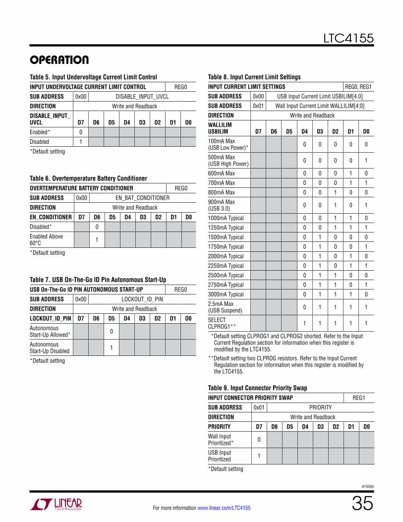
LTC4155
354155fd
For more information www.linear.com/LTC4155
Table 5. Input Undervoltage Current Limit ControlINPUT UNDERVOLTAGE CURRENT LIMIT CONTROL REG0
SUB ADDRESS 0x00 DISABLE_INPUT_UVCL
DIRECTION Write and Readback
DISABLE_INPUT_UVCL D7 D6 D5 D4 D3 D2 D1 D0
Enabled* 0
Disabled 1
*Default setting
Table 6. Overtemperature Battery ConditionerOVERTEMPERATURE BATTERY CONDITIONER REG0
SUB ADDRESS 0x00 EN_BAT_CONDITIONER
DIRECTION Write and Readback
EN_CONDITIONER D7 D6 D5 D4 D3 D2 D1 D0
Disabled* 0
Enabled Above 60°C 1
*Default setting
Table 7. USB On-The-Go ID Pin Autonomous Start-UpUSB On-The-Go ID PIN AUTONOMOUS START-UP REG0
SUB ADDRESS 0x00 LOCKOUT_ID_PIN
DIRECTION Write and Readback
LOCKOUT_ID_PIN D7 D6 D5 D4 D3 D2 D1 D0
Autonomous Start-Up Allowed* 0
Autonomous Start-Up Disabled 1
*Default setting
Table 8. Input Current Limit SettingsINPUT CURRENT LIMIT SETTINGS REG0, REG1
SUB ADDRESS 0x00 USB Input Current Limit USBILIM[4.0]
SUB ADDRESS 0x01 Wall Input Current Limit WALLILIM[4:0]
DIRECTION Write and Readback
WALLILIM USBILIM D7 D6 D5 D4 D3 D2 D1 D0
100mA Max (USB Low Power)* 0 0 0 0 0
500mA Max (USB High Power) 0 0 0 0 1
600mA Max 0 0 0 1 0
700mA Max 0 0 0 1 1
800mA Max 0 0 1 0 0
900mA Max (USB 3.0) 0 0 1 0 1
1000mA Typical 0 0 1 1 0
1250mA Typical 0 0 1 1 1
1500mA Typical 0 1 0 0 0
1750mA Typical 0 1 0 0 1
2000mA Typical 0 1 0 1 0
2250mA Typical 0 1 0 1 1
2500mA Typical 0 1 1 0 0
2750mA Typical 0 1 1 0 1
3000mA Typical 0 1 1 1 0
2.5mA Max (USB Suspend) 0 1 1 1 1
SELECT CLPROG1** 1 1 1 1 1
*Default setting CLPROG1 and CLPROG2 shorted. Refer to the Input Current Regulation section for information when this register is modified by the LTC4155.
**Default setting two CLPROG resistors. Refer to the Input Current Regulation section for information when this register is modified by the LTC4155.
Table 9. Input Connector Priority SwapINPUT CONNECTOR PRIORITY SWAP REG1
SUB ADDRESS 0x01 PRIORITY
DIRECTION Write and Readback
PRIORITY D7 D6 D5 D4 D3 D2 D1 D0
Wall Input Prioritized* 0
USB Input Prioritized 1
*Default setting
operaTion
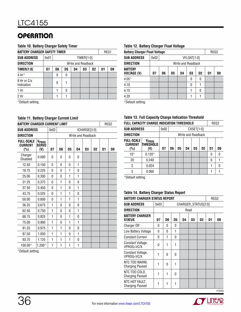
LTC4155
364155fd
For more information www.linear.com/LTC4155
Table 10. Battery Charger Safety TimerBATTERY CHARGER SAFETY TIMER REG1
SUB ADDRESS 0x01 TIMER[1:0]
DIRECTION Write and Readback
TIMER[1:0] D7 D6 D5 D4 D3 D2 D1 D0
4 Hr* 0 0
8 Hr or C/x Indication 0 1
1 Hr 1 0
2 Hr 1 1
*Default setting.
Table 11. Battery Charger Current LimitBATTERY CHARGER CURRENT LIMIT REG2
SUB ADDRESS 0x02 ICHARGE[3.0]
DIRECTION Write and Readback
FULL-SCALE CURRENT
(%)
VPROG SERVO
(V) D7 D6 D5 D4 D3 D2 D1 D0
Charger Disabled 0.000 0 0 0 0
12.50 0.150 0 0 0 1
18.75 0.225 0 0 1 0
25.00 0.300 0 0 1 1
31.25 0.375 0 1 0 0
37.50 0.450 0 1 0 1
43.75 0.525 0 1 1 0
50.00 0.600 0 1 1 1
56.25 0.675 1 0 0 0
62.50 0.750 1 0 0 1
68.75 0.825 1 0 1 0
75.00 0.900 1 0 1 1
81.25 0.975 1 1 0 0
87.50 1.050 1 1 0 1
93.75 1.125 1 1 1 0
100.00* 1.200* 1 1 1 1
*Default setting.
Table 12. Battery Charger Float VoltageBattery Charger Float Voltage REG2
SUB ADDRESS 0x02 VFLOAT[1:0]
DIRECTION Write and Readback
BATTERY VOLTAGE (V) D7 D6 D5 D4 D3 D2 D1 D0
4.05* 0 0
4.10 0 1
4.15 1 0
4.20 1 1
*Default setting.
Table 13. Full Capacity Charge Indication ThresholdFULL CAPACITY CHARGE INDICATION THRESHOLD REG2
SUB ADDRESS 0x02 CXSET[1:0]
DIRECTION Write and Readback
FULL-SCALE CURRENT
(%)
VPROG THRESHOLD
(V) D7 D6 D5 D4 D3 D2 D1 D0
10* 0.120* 0 0
20 0.240 0 1
2 0.024 1 0
5 0.060 1 1
*Default setting.
Table 14. Battery Charger Status ReportBATTERY CHARGER STATUS REPORT REG3
SUB ADDRESS 0x03 CHARGER_STATUS[2:0]
DIRECTION Read
BATTERY CHARGER STATUS D7 D6 D5 D4 D3 D2 D1 D0
Charger Off 0 0 0
Low Battery Voltage 0 0 1
Constant Current 0 1 0
Constant Voltage, VPROG>VC/X 0 1 1
Constant Voltage, VPROG<VC/X 1 0 0
NTC TOO WARM, Charging Paused 1 0 1
NTC TOO COLD, Charging Paused 1 1 0
NTC HOT FAULT, Charging Paused 1 1 1
operaTion
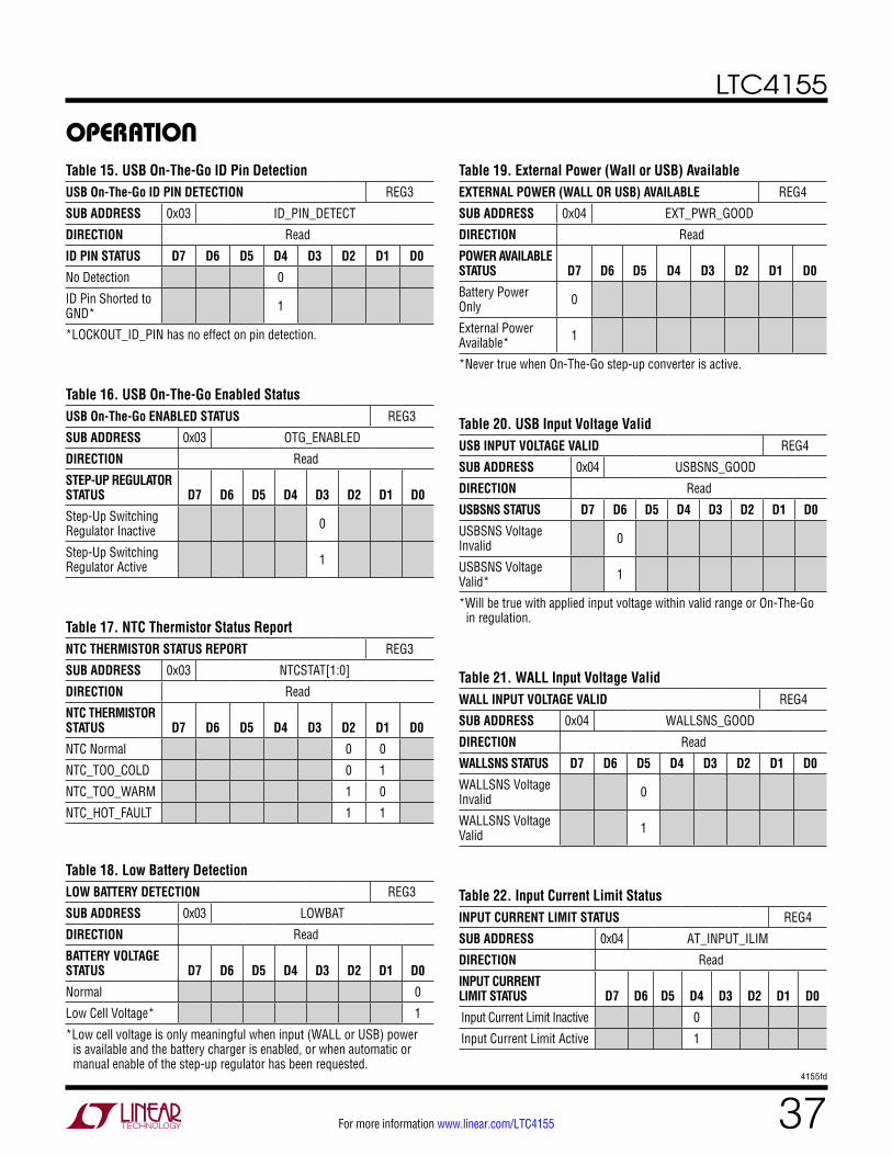
LTC4155
374155fd
For more information www.linear.com/LTC4155
Table 15. USB On-The-Go ID Pin DetectionUSB On-The-Go ID PIN DETECTION REG3
SUB ADDRESS 0x03 ID_PIN_DETECT
DIRECTION Read
ID PIN STATUS D7 D6 D5 D4 D3 D2 D1 D0
No Detection 0
ID Pin Shorted to GND* 1
*LOCKOUT_ID_PIN has no effect on pin detection.
Table 16. USB On-The-Go Enabled StatusUSB On-The-Go ENABLED STATUS REG3
SUB ADDRESS 0x03 OTG_ENABLED
DIRECTION Read
STEP-UP REGULATOR STATUS D7 D6 D5 D4 D3 D2 D1 D0
Step-Up Switching Regulator Inactive 0
Step-Up Switching Regulator Active 1
Table 17. NTC Thermistor Status ReportNTC THERMISTOR STATUS REPORT REG3
SUB ADDRESS 0x03 NTCSTAT[1:0]
DIRECTION Read
NTC THERMISTOR STATUS D7 D6 D5 D4 D3 D2 D1 D0
NTC Normal 0 0
NTC_TOO_COLD 0 1
NTC_TOO_WARM 1 0
NTC_HOT_FAULT 1 1
Table 18. Low Battery DetectionLOW BATTERY DETECTION REG3
SUB ADDRESS 0x03 LOWBAT
DIRECTION Read
BATTERY VOLTAGE STATUS D7 D6 D5 D4 D3 D2 D1 D0
Normal 0
Low Cell Voltage* 1
*Low cell voltage is only meaningful when input (WALL or USB) power is available and the battery charger is enabled, or when automatic or manual enable of the step-up regulator has been requested.
Table 19. External Power (Wall or USB) AvailableEXTERNAL POWER (WALL OR USB) AVAILABLE REG4
SUB ADDRESS 0x04 EXT_PWR_GOOD
DIRECTION Read
POWER AVAILABLE STATUS D7 D6 D5 D4 D3 D2 D1 D0
Battery Power Only 0
External Power Available* 1
*Never true when On-The-Go step-up converter is active.
Table 20. USB Input Voltage ValidUSB INPUT VOLTAGE VALID REG4
SUB ADDRESS 0x04 USBSNS_GOOD
DIRECTION Read
USBSNS STATUS D7 D6 D5 D4 D3 D2 D1 D0
USBSNS Voltage Invalid 0
USBSNS Voltage Valid* 1
*Will be true with applied input voltage within valid range or On-The-Go in regulation.
Table 21. WALL Input Voltage ValidWALL INPUT VOLTAGE VALID REG4
SUB ADDRESS 0x04 WALLSNS_GOOD
DIRECTION Read
WALLSNS STATUS D7 D6 D5 D4 D3 D2 D1 D0
WALLSNS Voltage Invalid 0
WALLSNS Voltage Valid 1
Table 22. Input Current Limit StatusINPUT CURRENT LIMIT STATUS REG4
SUB ADDRESS 0x04 AT_INPUT_ILIM
DIRECTION Read
INPUT CURRENT LIMIT STATUS D7 D6 D5 D4 D3 D2 D1 D0
Input Current Limit Inactive 0
Input Current Limit Active 1
operaTion

LTC4155
384155fd
For more information www.linear.com/LTC4155
Table 23. Input Undervoltage Current Limit (Brownout) StatusINPUT UNDERVOLTAGE CURRENT LIMIT (BROWNOUT) STATUS REG4
SUB ADDRESS 0x04 INPUT_UVCL_ACTIVE
DIRECTION Read
INPUT UNDERVOLTAGE CURRENT LIMIT STATUS D7 D6 D5 D4 D3 D2 D1 D0
Input UVCL Inactive 0
Input UVCL Active 1
Table 24. Overvoltage Protection FaultOVERVOLTAGE PROTECTION FAULT REG4
SUB ADDRESS 0x04 OVP_ACTIVE
DIRECTION Read
INPUT OVERVOLTAGE D7 D6 D5 D4 D3 D2 D1 D0
No Fault 0
Input (USB or WALL) Overvoltage 1
Table 25. USB On-The-Go Step-Up Regulator Fault ShutdownUSB On-The-Go STEP-UP REGULATOR FAULT SHUTDOWN REG4
SUB ADDRESS 0x04 OTG_FAULT
DIRECTION Read
STEP-UP REGULATOR STATUS D7 D6 D5 D4 D3 D2 D1 D0
No Fault 0
Regulator Over Current Shutdown 1
Table 26. Battery Unresponsive to ChargingBATTERY UNRESPONSIVE TO CHARGING REG4
SUB ADDRESS 0x04 BAD_CELL
DIRECTION Read
BATTERY STATUS D7 D6 D5 D4 D3 D2 D1 D0
No Fault 0
Low Cell Voltage Timeout 1
Table 27. NTC Analog-to-Digital Converter ResultNTC ANALOG-TO-DIGITAL CONVERTER RESULT REG5
SUB ADDRESS 0x05 NTCVAL[6:0]
DIRECTION Read
NTC CONVERSION RESULT D7 D6 D5 D4 D3 D2 D1 D0
NTCVAL[6:0]* d d d d d d d
See NTC Thermistor Monitor in Operation section to convert ADC result to temperature.
Table 28. NTC Temperature Out of Range for Battery ChargingNTC TEMPERATURE OUT OF RANGE FOR BATTERY CHARGING REG5
SUB ADDRESS 0x05 NTC_WARNING
DIRECTION Read
NTC TEMP RANGE D7 D6 D5 D4 D3 D2 D1 D0
Temperature Normal 0
Too Warm or Too Cold to Charge 1
Table 29. Battery Charger Interrupt MaskBATTERY CHARGER INTERRUPT MASK REG6
SUB ADDRESS 0x06 ENABLE_CHARGER_INT
DIRECTION Write and Readback
INTERRUPT ENABLE STATUS D7 D6 D5 D4 D3 D2 D1 D0
Charger Interrupts Disabled* 0
Charger Interrupts Enabled 1
*Default. Interrupt triggered by any change in CHARGER_STATUS[2:0].Any data written to sub address 0x06 has side effect of clearing any pending interrupt request.
operaTion
LTC4155
394155fd
For more information www.linear.com/LTC4155
Table 30. Fault Interrupt MaskFAULT INTERRUPT MASK REG6
SUB ADDRESS 0x06 ENABLE_FAULT_INT
DIRECTION Write and Readback
INTERRUPT ENABLE STATUS D7 D6 D5 D4 D3 D2 D1 D0
Fault Interrupts Disabled* 0
Fault Interrupts Enabled 1
*Default. Interrupt triggered by any change in OVP_ACTIVE, BAD_CELL, OTG_FAULT or NTC_HOT_FAULT. Any data written to sub address 0x06 has side effect of clearing any pending interrupt request.
Table 31. External Power Available Interrupt MaskEXTERNAL POWER AVAILABLE INTERRUPT MASK REG6
SUB ADDRESS 0x06 ENABLE_EXTPWR_INT
DIRECTION Write and Readback
INTERRUPT ENABLE STATUS D7 D6 D5 D4 D3 D2 D1 D0
External Power Interrupts Disabled*
0
External Power Interrupts Enabled 1
*Default. Interrupt triggered by any change in USBSNSGD, WALLSNSGD, or EXTPWRGD. Any data written to sub address 0x06 has side effect of clearing any pending interrupt request.
Table 32. USB On-The-Go Interrupt MaskUSB On-The-Go INTERRUPT MASK REG6
SUB ADDRESS 0x06 ENABLE_OTG_INT
DIRECTION Write and Readback
INTERRUPT ENABLE STATUS D7 D6 D5 D4 D3 D2 D1 D0
USB On-The-Go Interrupts Disabled* 0
USB On-The-Go Interrupts Enabled 1
*Default. Interrupt triggered by any change in EN_BOOST, ID_DETECT. Any data written to sub address 0x06 has side effect of clearing any pending interrupt request.
Table 33. Input Current Limit Interrupt MaskINPUT CURRENT LIMIT INTERRUPT MASK REG6
SUB ADDRESS 0x06 ENABLE_AT_ILIM_INT
DIRECTION Write and Readback
INTERRUPT ENABLE STATUS D7 D6 D5 D4 D3 D2 D1 D0
Input Current Limit Interrupts Disabled* 0
Input Current Limit Interrupts Enabled 1
*Default. Interrupt triggered by any change in AT_INPUT_ILIM. Any data written to sub address 0x06 has side effect of clearing any pending interrupt request.
operaTion
LTC4155
404155fd
For more information www.linear.com/LTC4155
Table 34. Input Undervoltage Current Limit (Brownout Detection) Interrupt MaskINPUT UNDERVOLTAGE CURRENT LIMIT (BROWNOUT DETECTION) INTERRUPT MASK REG6
SUB ADDRESS 0x06 ENABLE_INPUT_UVCL_INT
DIRECTION Write and Readback
INTERRUPT ENABLE STATUS D7 D6 D5 D4 D3 D2 D1 D0
Input Undervoltage Current Limit Interrupts Disabled*
0
Input Undervoltage Current Limit Interrupts Enabled
1
*Default. Interrupt triggered by any change in INPUT_UVCL_ACTIVE. Any data written to sub address 0x06 has side effect of clearing any pending interrupt request.
applicaTions inForMaTion
Figure 9. Alternate NTC Bias Network
Alternate NTC Thermistors and Biasing
The LTC4155 provides temperature qualified charging if a grounded thermistor and a bias resistor are connected to the NTC pin. Charging is paused if the temperature rises above an NTC_TOO_HOT limit or falls below an NTC_TOO_COLD limit. By using a Vishay curve 2 thermistor and a bias resis-tor whose value is equal to the room temperature resistance of the thermistor (r25), the upper and lower tempera- tures are preprogrammed to approximately 40°C and 0°C, respectively. The NTC_HOT_FAULT threshold which optionally generates an interrupt and/or enables the overtemperature battery conditioner is preprogrammed to approximately 60°C.
With minor modifications to the thermistor bias network as shown in Figure 9, it is possible to adjust either one or two of the three temperature thresholds with the constraint that it is usually not possible to move the temperature thresholds closer together. Intuitively, this would require increased temperature sensitivity from the thermistor.
operaTion
In the explanation below, the following notation is used.
r25 NTC thermistor value at 25°C.
RBIAS Low drift bias resistor, connected between the NTCBIAS and NTC pins.
Table 35. USB On-The-Go Step-Up Voltage Converter Manual ActivationUSB On-The-Go STEP-UP VOLTAGE CONVERTER MANUAL ACTIVATION REG6
SUB ADDRESS 0x06 REQUEST_OTG
DIRECTION Write and Readback
STEP-UP REGULATOR ACTIVATION D7 D6 D5 D4 D3 D2 D1 D0
Step-Up Regulator Activation Auto-matic or Disabled*
0
Enable Step-Up Voltage Regulator 1
*Default. Regulator cannot be activated if voltage is applied to either the USB or WALL inputs. Automatic activation controlled by LOCKOUT_ID_PIN. Any data written to sub address 0x06 has side effect of clearing any pending interrupt request.
RNTC
RBIAS
LTC4155
4155 F09
NTC
NTCBIAS
T
RTEMP_RANGE
LTC4155
414155fd
For more information www.linear.com/LTC4155
applicaTions inForMaTionRTEMP_RANGE
Optional dilution resistor, connected in series with the thermistor.
αT ≡ rT
r25 Thermistor resistance ratio at any temperature T relative to its reference temperature.
αTOO _ COLD ≡ rTOO _ COLD
r25 Thermistor resistance ratio at desired NTC_TOO_COLD threshold temperature relative to its reference temperature.
αTOO _ WARM ≡ rTOO _ WARM
r25 Thermistor resistance ratio at desired NTC_TOO_WARM threshold temperature relative to its reference temperature.
αHOT _FAULT ≡ rHOT _FAULT
r25 Thermistor resistance ratio at desired NTC_HOT_FAULT threshold temperature relative to its reference tem-perature.
αBIAS ≡ RBIAS
r25 Ratio of low drift bias resistor to r25.
αTEMP _RANGE ≡ RTEMP _RANGE
r25
Ratio of optional low drift dilution resistor to r25.
Note that r25, rT, rTOO_COLD, rTOO_WARM, and rHOT_FAULT and are all resistance values of the thermistor at different temperatures, while RBIAS and RTEMP_RANGE are actual low drift resistors.
In all of the following calculations, it will be necessary to determine the thermistor’s αT at various temperatures.
This parameter is dependent only upon the material prop-erties of the thermistor. αT for a given thermistor and temperature may be found in one of two ways. Thermistor manufacturers often provide a lookup table relating αT to temperature in their data sheets. For any temperature T, αT may be referenced directly.
The second way to obtain αT for any T requires the use of a modeling equation and a material constant specific to the thermistor:
αT = eb 1
T
− 1
T0
where:
e = Natural logarithm base, approximately 2.71828
T = Temperature of interest, expressed in Kelvin
T0 = Thermistor model nominal temperature, expressed in Kelvin. Typically 298.15K (25°C + 273.15°C)
b = Model material constant, expressed in Kelvin. This model is a curve fit at T0 and a second temperature. b is close to 4000K for most thermistors. Higher b results in increased temperature sensitivity at the expense of reduced linearity over a wide temperature range
Simple Alternate Thermistor Bias Network
By simply adjusting the bias resistor, RBIAS, and omitting the optional RTEMP_RANGE, one of the three temperature thresholds may be adjusted. The other two temperature comparator thresholds will be determined by the choice of the first temperature threshold and the NTCVAL thresholds fixed in the LTC4155. Increasing RBIAS above r25 shifts all three temperature thresholds colder while simultaneously slightly compressing the temperature span between thresholds. Likewise, decreasing RBIAS below r25 shifts all three temperature thresholds warmer while simultaneously slightly expanding the temperature span between thresholds. To program a single temperature threshold, obtain the value of either αTOO_COLD, αTOO_WARM or αHOT_FAULT for the chosen temperature threshold using one of the aforementioned methods and
LTC4155
424155fd
For more information www.linear.com/LTC4155
applicaTions inForMaTionsubstitute into the appropriate following equation to cal-culate the value αBIAS and then RBIAS.
αBIAS = 0.34917 • αTOO_COLD
αBIAS = 1.73735 • αTOO_WARM
αBIAS = 3.35249 • αHOT_FAULT
RBIAS = αBIAS • r25
With αBIAS for the newly programmed temperature threshold now determined, the other two dependent tem-perature thresholds may be found by substituting αBIAS into the remaining two equations. The following equation may be used to convert any other NTC ADC result (NTCVAL)back to a resistance ratio by substituting the kSPAN and kOFFSET values found in the Electrical Characteristics table.
αT = kSPAN • NTCVAL + kOFFSET
1− kSPAN • NTCVAL – kOFFSET
αBIAS
αT may then be used to determine the temperature using either the lookup table provided by the thermistor manu-facturer or the curve fit model:
T = b
ln (αT )+ bT0
Advanced Alternate Thermistor Bias Network
If an adjustment to RBIAS does not yield an acceptable span between temperature thresholds, a second low drift bias resistor may be added to the bias network between the NTC pin and the top of the thermistor. This resistor has the net effect of diluting the high thermal sensitivity of the thermistor with low drift resistance. The result is reduced thermal gain and a wider temperature span between the preprogrammed voltage thresholds of the LTC4155. Using this additional resistor, two of the three temperature comparator thresholds may be adjusted. The remaining threshold is constrained by the limited degrees of freedom of the bias network. After determining the αT values for the two temperature thresholds of interest, the following equations may be used to determine αBIAS, αTEMP_RANGE, and the third constrained temperature threshold dependent on the choice of bias network and the thermistor.
To specify TTOO_COLD and TTOO_WARM, then calculate THOT_FAULT:
αTEMP_RANGE = 0.25153 • αTOO_COLD – 1.25153 • αTOO_WARM
RTEMP_RANGE = αTEMP_RANGE • r25
αBIAS = 0.43699 • (αTOO_COLD – αTOO_WARM)
RBIAS = αBIAS • r25
With the bias network determined, the overconstrained threshold may then be calculated:
αHOT_FAULT = 0.29829 • αBIAS – αTEMP_RANGE
To specify TTOO_COLD and THOT_FAULT, then calculate TTOO_WARM:
αTEMP_RANGE = 0.11626 • αTOO_COLD – 1.11626 • αHOT_FAULT
RTEMP_RANGE = αTEMP_RANGE • r25
αBIAS = 0.38976 • (αTOO_COLD – αHOT_FAULT)
RBIAS = αBIAS • r25
With the bias network determined, the overconstrained threshold may then be calculated:
αTOO_WARM = 0.57559 • αBIAS – αTEMP_RANGE
To specify TTOO_WARM and THOT_FAULT, then calculate TTOO_COLD:
αTEMP_RANGE = 1.07566 • αTOO_WARM – 2.07566 • αHOT_FAULT
RTEMP_RANGE = αTEMP_RANGE • r25
αBIAS = 3.60615 • (αTOO_WARM – αHOT_FAULT)
RBIAS = αBIAS • r25
With the bias network determined, the overconstrained threshold may then be calculated:
αTOO_COLD = 2.863946 • αBIAS – αTEMP_RANGE
It is possible to obtain a negative result for RTEMP_RANGE which is not physically realizable using the previous equa-tions. A negative result indicates that the two chosen tem-perature thresholds are too close in temperature and require more thermal sensitivity than the thermistor can provide.
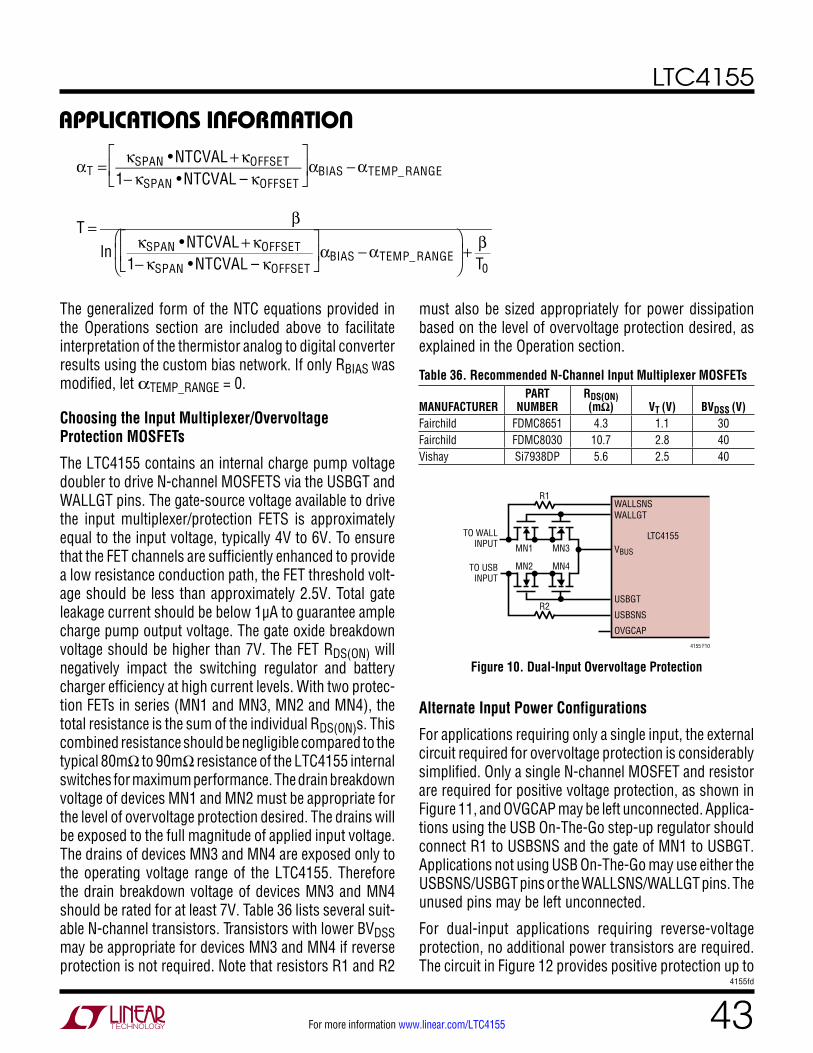
LTC4155
434155fd
For more information www.linear.com/LTC4155
The generalized form of the NTC equations provided in the Operations section are included above to facilitate interpretation of the thermistor analog to digital converter results using the custom bias network. If only RBIAS was modified, let αTEMP_RANGE = 0.
Choosing the Input Multiplexer/Overvoltage Protection MOSFETs
The LTC4155 contains an internal charge pump voltage doubler to drive N-channel MOSFETS via the USBGT and WALLGT pins. The gate-source voltage available to drive the input multiplexer/protection FETS is approximately equal to the input voltage, typically 4V to 6V. To ensure that the FET channels are sufficiently enhanced to provide a low resistance conduction path, the FET threshold volt-age should be less than approximately 2.5V. Total gate leakage current should be below 1µA to guarantee ample charge pump output voltage. The gate oxide breakdown voltage should be higher than 7V. The FET RDS(ON) will negatively impact the switching regulator and battery charger efficiency at high current levels. With two protec-tion FETs in series (MN1 and MN3, MN2 and MN4), the total resistance is the sum of the individual RDS(ON)s. This combined resistance should be negligible compared to the typical 80mΩ to 90mΩ resistance of the LTC4155 internal switches for maximum performance. The drain breakdown voltage of devices MN1 and MN2 must be appropriate for the level of overvoltage protection desired. The drains will be exposed to the full magnitude of applied input voltage. The drains of devices MN3 and MN4 are exposed only to the operating voltage range of the LTC4155. Therefore the drain breakdown voltage of devices MN3 and MN4 should be rated for at least 7V. Table 36 lists several suit-able N-channel transistors. Transistors with lower BVDSS may be appropriate for devices MN3 and MN4 if reverse protection is not required. Note that resistors R1 and R2
must also be sized appropriately for power dissipation based on the level of overvoltage protection desired, as explained in the Operation section.
Table 36. Recommended N-Channel Input Multiplexer MOSFETs
MANUFACTURERPART
NUMBERRDS(ON) (mΩ) VT (V) BVDSS (V)
Fairchild FDMC8651 4.3 1.1 30Fairchild FDMC8030 10.7 2.8 40Vishay Si7938DP 5.6 2.5 40
applicaTions inForMaTion
αT = kSPAN •NTCVAL + kOFFSET
1− kSPAN •NTCVAL – kOFFSET
αBIAS − αTEMP_RANGE
T = b
ln kSPAN •NTCVAL + kOFFSET1− kSPAN •NTCVAL – kOFFSET
αBIAS − αTEMP_RANGE
+ b
T0
Figure 10. Dual-Input Overvoltage Protection
Alternate Input Power Configurations
For applications requiring only a single input, the external circuit required for overvoltage protection is considerably simplified. Only a single N-channel MOSFET and resistor are required for positive voltage protection, as shown in Figure 11, and OVGCAP may be left unconnected. Applica-tions using the USB On-The-Go step-up regulator should connect R1 to USBSNS and the gate of MN1 to USBGT. Applications not using USB On-The-Go may use either the USBSNS/USBGT pins or the WALLSNS/WALLGT pins. The unused pins may be left unconnected.
For dual-input applications requiring reverse-voltage protection, no additional power transistors are required. The circuit in Figure 12 provides positive protection up to
VBUS
TO USBINPUT
TO WALLINPUT
OVGCAP
USBGT
USBSNS
WALLGT
LTC4155
WALLSNS
4155 F10
MN1
R1
R2
MN3
MN2 MN4
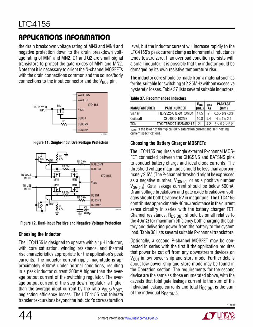
LTC4155
444155fd
For more information www.linear.com/LTC4155
Figure 11. Single-Input Overvoltage Protection
Figure 12. Dual-Input Positive and Negative Voltage Protection
the drain breakdown voltage rating of MN3 and MN4 and negative protection down to the drain breakdown volt-age rating of MN1 and MN2. Q1 and Q2 are small-signal transistors to protect the gate oxides of MN1 and MN2. Note that it is necessary to orient the N-channel MOSFETs with the drain connections common and the source/body connections to the input connector and the VBUS pin.
level, but the inductor current will increase rapidly to the LTC4155’s peak current clamp as incremental inductance tends toward zero. If an overload condition persists with a small inductor, it is possible that the inductor could be damaged by its own resistive temperature rise.
The inductor core should be made from a material such as ferrite, suitable for switching at 2.25MHz without excessive hysteretic losses. Table 37 lists several suitable inductors.
Table 37. Recommended Inductors
MANUFACTURER PART NUMBERRDC
(mΩ)IMAX (A)
PACKAGE (mm)
Vishay IHLP2525AHE-B1ROMO1 17.5 7 6.5 × 6.9 × 3.2Coilcraft XFL4020-102ME 10.8 5.4 4 × 4 × 2.1TDK TDKLTF5022T1R2N4R2-LF 21 4.2 5 × 5.2 × 2.2IMAX is the lower of the typical 30% saturation current and self-heating current specifications.
Choosing the Battery Charger MOSFETs
The LTC4155 requires a single external P-channel MOS-FET connected between the CHGSNS and BATSNS pins to conduct battery charge and ideal diode currents. The threshold voltage magnitude should be less than approxi-mately 2.5V. (The P-channel threshold might be expressed as a negative number, VGS(th), or as a positive number VSG(th)). Gate leakage current should be below 500nA. Drain voltage breakdown and gate oxide breakdown volt-ages should both be above 5V in magnitude. The LTC4155 contributes approximately 40mΩ resistance in the current sense circuitry in series with the battery charger FET. Channel resistance, RDS(ON), should be small relative to the 40mΩ for maximum efficiency both charging the bat-tery and delivering power from the battery to the system load. Table 38 lists several suitable P-channel transistors.
Optionally, a second P-channel MOSFET may be con-nected in series with the first if the application requires that power be cut off from any downstream devices on VOUT in low power ship-and-store mode. Further details about low power ship-and-store mode may be found in the Operation section. The requirements for the second device are the same as those enumerated above, with the caveats that total gate leakage current is the sum of the individual leakage currents and total RDS(ON) is the sum of the individual RDS(ON)s.
applicaTions inForMaTion
VBUSTO POWER
INPUT
OVGCAP
USBGT
USBSNS
WALLGT
LTC4155
WALLSNS
4155 F11
R1
MN1
VBUSTO USB
INPUT
TO WALLINPUT
OVGCAP
USBGT
USBSNS
WALLGT
LTC4155
WALLSNS
4155 F12
MN1
R547k
R647k C1
OPT0.01µF
R3 5M
R4 5M
R1 3.6k
R2 3.6k
MN3
MN2 MN4
Q1
Q2
Q3
Q4
Choosing the Inductor
The LTC4155 is designed to operate with a 1µH inductor, with core saturation, winding resistance, and thermal rise characteristics appropriate for the application’s peak currents. The inductor current ripple magnitude is ap-proximately 400mA under normal conditions, resulting in a peak inductor current 200mA higher than the aver-age output current of the switching regulator. The aver-age output current of the step-down regulator is higher than the average input current by the ratio VBUS/VOUT, neglecting efficiency losses. The LTC4155 can tolerate transient excursions beyond the inductor’s core saturation
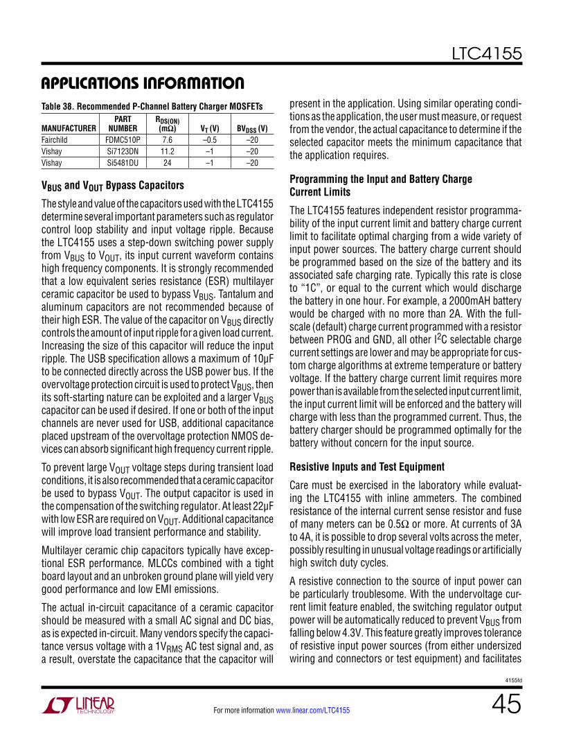
LTC4155
454155fd
For more information www.linear.com/LTC4155
Table 38. Recommended P-Channel Battery Charger MOSFETs
MANUFACTURERPART
NUMBERRDS(ON) (mΩ) VT (V) BVDSS (V)
Fairchild FDMC510P 7.6 –0.5 –20Vishay Si7123DN 11.2 –1 –20Vishay Si5481DU 24 –1 –20
VBUS and VOUT Bypass Capacitors
The style and value of the capacitors used with the LTC4155 determine several important parameters such as regulator control loop stability and input voltage ripple. Because the LTC4155 uses a step-down switching power supply from VBUS to VOUT, its input current waveform contains high frequency components. It is strongly recommended that a low equivalent series resistance (ESR) multilayer ceramic capacitor be used to bypass VBUS. Tantalum and aluminum capacitors are not recommended because of their high ESR. The value of the capacitor on VBUS directly controls the amount of input ripple for a given load current. Increasing the size of this capacitor will reduce the input ripple. The USB specification allows a maximum of 10μF to be connected directly across the USB power bus. If the overvoltage protection circuit is used to protect VBUS, then its soft-starting nature can be exploited and a larger VBUS capacitor can be used if desired. If one or both of the input channels are never used for USB, additional capacitance placed upstream of the overvoltage protection NMOS de-vices can absorb significant high frequency current ripple.
To prevent large VOUT voltage steps during transient load conditions, it is also recommended that a ceramic capacitor be used to bypass VOUT. The output capacitor is used in the compensation of the switching regulator. At least 22μF with low ESR are required on VOUT. Additional capacitance will improve load transient performance and stability.
Multilayer ceramic chip capacitors typically have excep-tional ESR performance. MLCCs combined with a tight board layout and an unbroken ground plane will yield very good performance and low EMI emissions.
The actual in-circuit capacitance of a ceramic capacitor should be measured with a small AC signal and DC bias, as is expected in-circuit. Many vendors specify the capaci-tance versus voltage with a 1VRMS AC test signal and, as a result, overstate the capacitance that the capacitor will
present in the application. Using similar operating condi-tions as the application, the user must measure, or request from the vendor, the actual capacitance to determine if the selected capacitor meets the minimum capacitance that the application requires.
Programming the Input and Battery Charge Current Limits
The LTC4155 features independent resistor programma-bility of the input current limit and battery charge current limit to facilitate optimal charging from a wide variety of input power sources. The battery charge current should be programmed based on the size of the battery and its associated safe charging rate. Typically this rate is close to “1C”, or equal to the current which would discharge the battery in one hour. For example, a 2000mAH battery would be charged with no more than 2A. With the full-scale (default) charge current programmed with a resistor between PROG and GND, all other I2C selectable charge current settings are lower and may be appropriate for cus-tom charge algorithms at extreme temperature or battery voltage. If the battery charge current limit requires more power than is available from the selected input current limit, the input current limit will be enforced and the battery will charge with less than the programmed current. Thus, the battery charger should be programmed optimally for the battery without concern for the input source.
Resistive Inputs and Test Equipment
Care must be exercised in the laboratory while evaluat-ing the LTC4155 with inline ammeters. The combined resistance of the internal current sense resistor and fuse of many meters can be 0.5Ω or more. At currents of 3A to 4A, it is possible to drop several volts across the meter, possibly resulting in unusual voltage readings or artificially high switch duty cycles.
A resistive connection to the source of input power can be particularly troublesome. With the undervoltage cur-rent limit feature enabled, the switching regulator output power will be automatically reduced to prevent VBUS from falling below 4.3V. This feature greatly improves tolerance of resistive input power sources (from either undersized wiring and connectors or test equipment) and facilitates
applicaTions inForMaTion
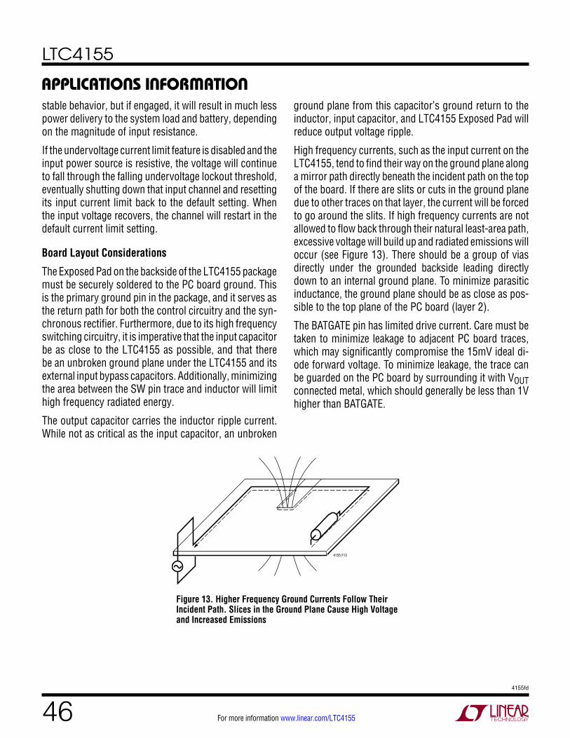
LTC4155
464155fd
For more information www.linear.com/LTC4155
stable behavior, but if engaged, it will result in much less power delivery to the system load and battery, depending on the magnitude of input resistance.
If the undervoltage current limit feature is disabled and the input power source is resistive, the voltage will continue to fall through the falling undervoltage lockout threshold, eventually shutting down that input channel and resetting its input current limit back to the default setting. When the input voltage recovers, the channel will restart in the default current limit setting.
Board Layout Considerations
The Exposed Pad on the backside of the LTC4155 package must be securely soldered to the PC board ground. This is the primary ground pin in the package, and it serves as the return path for both the control circuitry and the syn-chronous rectifier. Furthermore, due to its high frequency switching circuitry, it is imperative that the input capacitor be as close to the LTC4155 as possible, and that there be an unbroken ground plane under the LTC4155 and its external input bypass capacitors. Additionally, minimizing the area between the SW pin trace and inductor will limit high frequency radiated energy.
The output capacitor carries the inductor ripple current. While not as critical as the input capacitor, an unbroken
ground plane from this capacitor’s ground return to the inductor, input capacitor, and LTC4155 Exposed Pad will reduce output voltage ripple.
High frequency currents, such as the input current on the LTC4155, tend to find their way on the ground plane along a mirror path directly beneath the incident path on the top of the board. If there are slits or cuts in the ground plane due to other traces on that layer, the current will be forced to go around the slits. If high frequency currents are not allowed to flow back through their natural least-area path, excessive voltage will build up and radiated emissions will occur (see Figure 13). There should be a group of vias directly under the grounded backside leading directly down to an internal ground plane. To minimize parasitic inductance, the ground plane should be as close as pos-sible to the top plane of the PC board (layer 2).
The BATGATE pin has limited drive current. Care must be taken to minimize leakage to adjacent PC board traces, which may significantly compromise the 15mV ideal di-ode forward voltage. To minimize leakage, the trace can be guarded on the PC board by surrounding it with VOUT connected metal, which should generally be less than 1V higher than BATGATE.
Figure 13. Higher Frequency Ground Currents Follow Their Incident Path. Slices in the Ground Plane Cause High Voltage and Increased Emissions
applicaTions inForMaTion
4155 F13
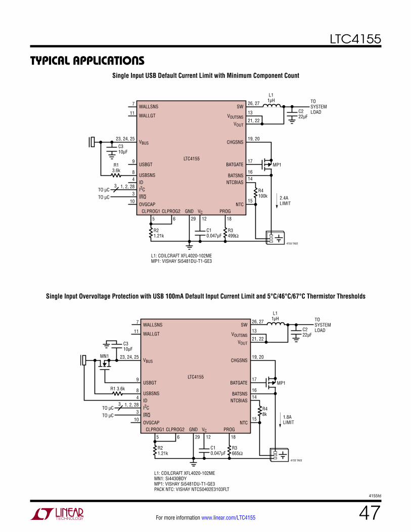
LTC4155
474155fd
For more information www.linear.com/LTC4155
Typical applicaTions
7
11
84
3 1, 2, 283
10
5 6 29 12 18
4155 TA02
15
14
R3499Ω
C10.047µF
9
23, 24, 25
R13.6k
R21.21k
L1: COILCRAFT XFL4020-102MEMP1: VISHAY Si5481DU-T1-GE3
R4100k 2.4A
LIMIT
C222µF
TOSYSTEMLOAD
C310µF
TO µC
TO µC
WALLSNS SW
WALLGT
VBUS
USBGT
USBSNS
CLPROG1 CLPROG2 GND PROGVC
ID NTCBIAS
16
17MP1
BATSNS
BATGATE
19, 20
26, 27
L11µH
VOUTSNS13
VOUT21, 22
CHGSNS
LTC4155
I2C
IRQ
OVGCAP NTC
Single Input USB Default Current Limit with Minimum Component Count
Single Input Overvoltage Protection with USB 100mA Default Input Current Limit and 5°C/46°C/67°C Thermistor Thresholds
7
11
84
3 1, 2, 283
10
5 6 29 12 18
4155 TA03
15
14
R3665Ω
C10.047µF
9
23, 24, 25
R1 3.6k
MN1
C310µF
R21.21k
R48k
C222µF
TOSYSTEMLOAD
TO µC
TO µC
WALLSNS SW
WALLGT
VBUS
USBGT
USBSNS
CLPROG1 CLPROG2 GND PROGVC
ID NTCBIAS
16
17MP1
BATSNS
BATGATE
19, 20
26, 27
L11µH
VOUTSNS13
VOUT21, 22
CHGSNS
LTC4155
I2C
IRQ
OVGCAP NTC1.8ALIMIT
L1: COILCRAFT XFL4020-102MEMN1: Si4430BDYMP1: VISHAY Si5481DU-T1-GE3PACK NTC: VISHAY NTCS0402E3103FLT
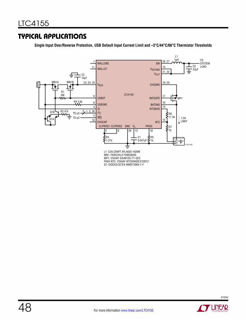
LTC4155
484155fd
For more information www.linear.com/LTC4155
Single Input Over/Reverse Protection, USB Default Input Current Limit and –3°C/44°C/66°C Thermistor Thresholds
7
11
84
3 1, 2, 283
10
5 6 29 12 18
4155 TA04
15
14
R51k
C10.047µF
9
23, 24, 25
R15M
R3 47k
R4 3.6k
MN1B
C310µF
MN1A
R41.21k
R611.5k
R71k
C222µF
TOSYSTEMLOAD
TO µC
TO µC
WALLSNS SW
WALLGT
VBUS
USBGT
USBSNS
CLPROG1 CLPROG2 GND PROGVC
ID NTCBIAS
16
17MP1
BATSNS
BATGATE
19, 20
26, 27
L11µH
VOUTSNS13
VOUT21, 22
CHGSNS
LTC4155
I2C
IRQ
OVGCAP NTCQ1A
Q1B
1.2ALIMIT
L1: COILCRAFT XFL4020-102MEMN1: FAIRCHILD FDMC8030MP1: VISHAY Si5481DU-T1-GE3PACK NTC: VISHAY NTCS0402E3103FLTQ1: DIODES/ZETEX MMDT3904-7-F
Typical applicaTions
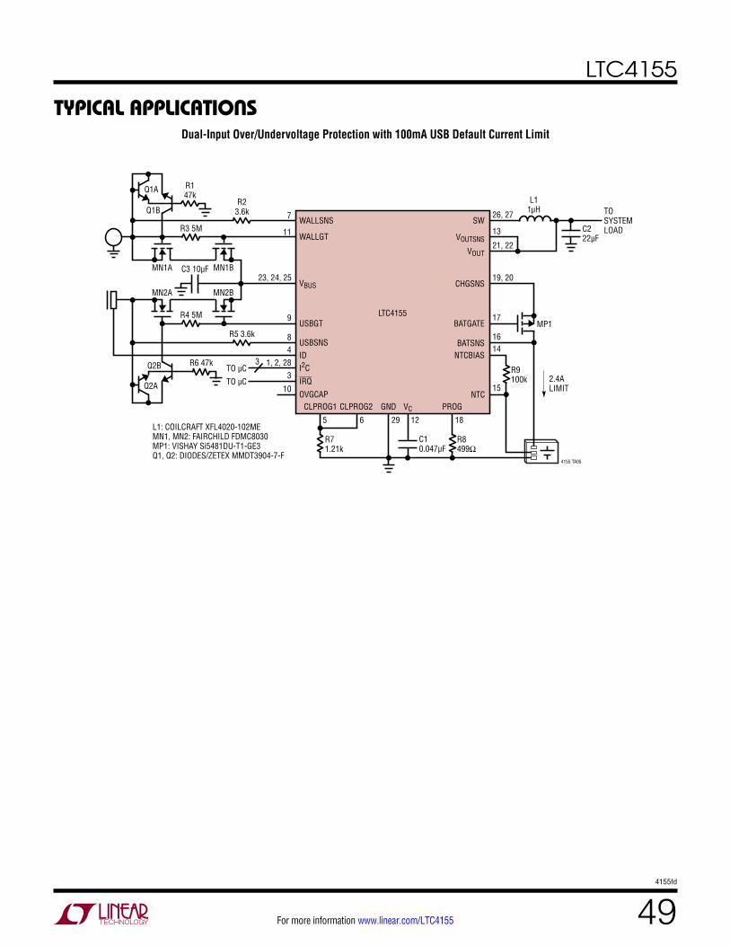
LTC4155
494155fd
For more information www.linear.com/LTC4155
Dual-Input Over/Undervoltage Protection with 100mA USB Default Current Limit
Typical applicaTions
7
R23.6k
R147k
11
84
3 1, 2, 283
10
5 6 29 12 18
4155 TA05
15
14
R8499Ω
C10.047µF
9
23, 24, 25
R3 5M
R4 5M
R6 47k
R5 3.6k
MN1B
MN2B
C3 10µFMN1A
MN2A
Q1A
Q1B
R71.21k
R9100k
C222µF
TOSYSTEMLOAD
Q2A
Q2B TO µC
TO µC
WALLSNS SW
WALLGT
VBUS
USBGT
USBSNS
CLPROG1 CLPROG2 GND PROGVC
ID NTCBIAS
16
17MP1
BATSNS
BATGATE
19, 20
26, 27
L11µH
VOUTSNS13
VOUT21, 22
CHGSNS
LTC4155
I2C
IRQ
OVGCAP NTC
2.4ALIMIT
L1: COILCRAFT XFL4020-102MEMN1, MN2: FAIRCHILD FDMC8030MP1: VISHAY Si5481DU-T1-GE3Q1, Q2: DIODES/ZETEX MMDT3904-7-F
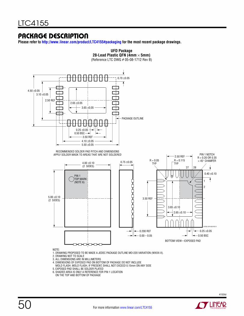
LTC4155
504155fd
For more information www.linear.com/LTC4155
4.00 ±0.10(2 SIDES)
2.50 REF
5.00 ±0.10(2 SIDES)
NOTE:1. DRAWING PROPOSED TO BE MADE A JEDEC PACKAGE OUTLINE MO-220 VARIATION (WXXX-X).2. DRAWING NOT TO SCALE3. ALL DIMENSIONS ARE IN MILLIMETERS4. DIMENSIONS OF EXPOSED PAD ON BOTTOM OF PACKAGE DO NOT INCLUDE MOLD FLASH. MOLD FLASH, IF PRESENT, SHALL NOT EXCEED 0.15mm ON ANY SIDE5. EXPOSED PAD SHALL BE SOLDER PLATED6. SHADED AREA IS ONLY A REFERENCE FOR PIN 1 LOCATION ON THE TOP AND BOTTOM OF PACKAGE
PIN 1TOP MARK(NOTE 6)
0.40 ±0.10
27 28
1
2
BOTTOM VIEW—EXPOSED PAD
3.50 REF
0.75 ±0.05 R = 0.115TYP
R = 0.05TYP
PIN 1 NOTCHR = 0.20 OR 0.35× 45° CHAMFER
0.25 ±0.05
0.50 BSC
0.200 REF
0.00 – 0.05
(UFD28) QFN 0506 REV B
RECOMMENDED SOLDER PAD PITCH AND DIMENSIONSAPPLY SOLDER MASK TO AREAS THAT ARE NOT SOLDERED
0.70 ±0.05
0.25 ±0.050.50 BSC
2.50 REF
3.50 REF4.10 ±0.055.50 ±0.05
2.65 ±0.05
3.10 ±0.054.50 ±0.05
PACKAGE OUTLINE
2.65 ±0.10
3.65 ±0.10
3.65 ±0.05
UFD Package28-Lead Plastic QFN (4mm × 5mm)
(Reference LTC DWG # 05-08-1712 Rev B)
package DescripTionPlease refer to http://www.linear.com/product/LTC4155#packaging for the most recent package drawings.
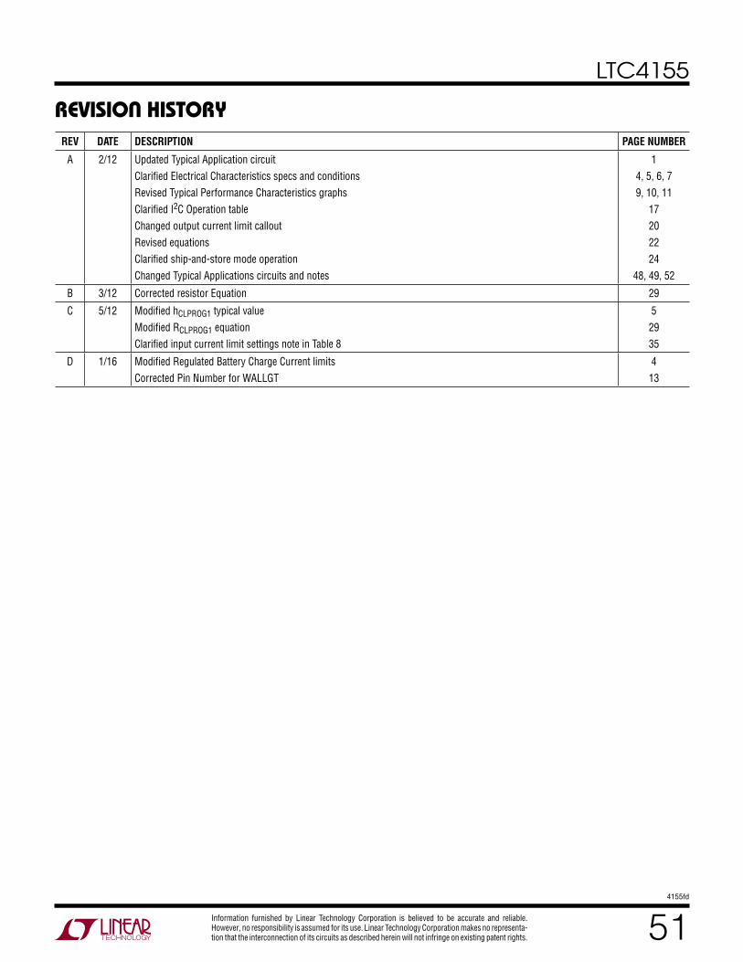
LTC4155
514155fd
For more information www.linear.com/LTC4155
Information furnished by Linear Technology Corporation is believed to be accurate and reliable. However, no responsibility is assumed for its use. Linear Technology Corporation makes no representa-tion that the interconnection of its circuits as described herein will not infringe on existing patent rights.
revision hisToryREV DATE DESCRIPTION PAGE NUMBER
A 2/12 Updated Typical Application circuitClarified Electrical Characteristics specs and conditionsRevised Typical Performance Characteristics graphsClarified I2C Operation tableChanged output current limit calloutRevised equationsClarified ship-and-store mode operationChanged Typical Applications circuits and notes
14, 5, 6, 79, 10, 11
17202224
48, 49, 52
B 3/12 Corrected resistor Equation 29
C 5/12 Modified hCLPROG1 typical valueModified RCLPROG1 equationClarified input current limit settings note in Table 8
52935
D 1/16 Modified Regulated Battery Charge Current limitsCorrected Pin Number for WALLGT
413
LTC4155
524155fd
For more information www.linear.com/LTC4155Linear Technology Corporation1630 McCarthy Blvd., Milpitas, CA 95035-7417
LINEAR TECHNOLOGY CORPORATION 2011
LT 0116 REV D • PRINTED IN USA
(408) 432-1900 ● FAX: (408) 434-0507 ● www.linear.com/LTC4155
relaTeD parTs
Typical applicaTionDual-Input Overvoltage Protection with 1.21A Default Input Current Limit and Output Voltage Disconnect
7
R13.6k
11
84
3 1, 2, 283
10
5 6 29 12 18
4155 TA06
15
14
R5340Ω
C20.047µF
C10.01µF
9
23, 24, 25
R2 3.6k
MN1B
MN2B
C4 10µFMN1A
MN2A
R31k
R41.21k
R6100k
C322µF
TOSYSTEMLOAD
TO µC
TO µC
WALLSNS SW
WALLGT
VBUS
USBGT
USBSNS
CLPROG1 CLPROG2 GND PROGVC
ID NTCBIAS
16
17MP2
BATSNS
BATGATE
19, 20
26, 27
L11µH
VOUTSNS13
VOUT21, 22
CHGSNS
LTC4155
I2C
IRQ
OVGCAP NTC
MP1
L1: COILCRAFT XFL4020-102MEMN1, MN2: FAIRCHILD FDMC8030MP1, MP2: VISHAY, Si5481DU-T1-GE3
3.52ALIMIT
PART NUMBER DESCRIPTION COMMENTS
LTC4156 Dual-Input Power Manager/3.5A LiFePO4 Battery Charger with I2C Control and USB OTG
High Efficiency Charger Capable of 3.5A Charge Current, Monolithic Switching Regulator Makes Optimal Use of Limited Power and Thermal Budget, Dual Input Overvoltage Protection Controller, Priority Multiplexing for Multiple Inputs, I2C/SMBus Control and Status Feedback, NTC Thermistor ADC for Temperature Dependent Charge Algorithms (JEITA), Instant-On Operation with Low Battery, Battery Ideal Diode Controller for Poser Management, USB On-The-Go Delivery to the USB Port, Full Featured LifePO4 Battery Charger with Four Float Voltage Settings, 28-Lead 4mm × 5mm QFN Package
LTC4088 High Efficiency USB Power Manager and Battery Charger
Maximizes Available Power from USB Port, Bat-Track™, Instant-On Operation, 1.5A Max Charge Current, 3mm × 4mm DFN-14 Package
LTC4089/LTC4089-1 LTC4089-5
High Voltage USB Power Manager with Ideal Diode Controller and High Efficiency Li-Ion Battery Charger
High Efficiency 1.2A Charger from 6V to 36V (40V Max) Input; Bat-Track Adaptive Output Control (LTC4089); Fixed 5V Output (LTC4089-5/LTC4089-1); LTC4089-1 for 4.1V Float Voltage Batteries, 3mm × 6mm DFN-22 Package;
LTC4090/LTC4090-5 High Voltage USB Power Manager with Ideal Diode Controller and High Efficiency Li-Ion Battery Charger
High Efficiency 1.2A Charger from 6V to 38V (60V Max) Input Bat-Track Adaptive Output Control; LTC4090-5 Has No Bat-Track. 3mm × 6mm DFN-22 Package
LTC4098/LTC4098-1 USB-Compatible Switchmode Power Manager with OVP
66V OVP. 1.5A Max Charge Current from Wall, 600mA Charge Current from USB, LTC4098-1 Has 4.1V VFLOAT, 3mm × 4mm QFN-20 Package
LTC4099 I2C Controlled USB Switchmode Power Manager with OVP
66V OVP. I2C for Control and Status Readback, 1.5A Max Charge Current from Wall, 600mA Charge Current from USB, 3mm × 4mm QFN-20 Package
LTC4160/LTC4160-1 Switchmode Power Manager with OVP and USB-OTG
USB-OTG 5V Output, Overvoltage Protection, Maximizes Available Power from USB Port, Bat-Track, Instant-On Operation, 1.5A Max Charge Current from Wall, 600mA Charge Current from USB, 3mm × 4mm QFN-20 Package
LTC4098-3.6 USB-Compatible Switchmode LiFePO4 Power Manager with OVP
3.6V VFLOAT for LiFePO4 Cells; 66V OVP. 1.5A Max Charge Current from Wall, 600mA Charge Current from USB, 3mm × 4mm QFN-20 Package
Mouser Electronics
Authorized Distributor
Click to View Pricing, Inventory, Delivery & Lifecycle Information: Analog Devices Inc.:
LTC4155IUFD#PBF LTC4155EUFD#PBF LTC4155IUFD#TRPBF LTC4155EUFD#TRPBF