Embed Size (px)
Citation preview

Doc.No. Rev.No Page / 31LTN140AT26-L01 104-A03-G-120220
Samsung Secret
Approval
NOTE : Extension code [ -L01 ]→ LTN140AT26-L01
- Surface type [ Glare ]
TO DATE
: Lenovo: Feb. 20. 2012
SAMSUNG TFT-LCD
MODEL NO. : LTN140AT26-L01
APPROVED BY :
PREPARED BY :
Michael Kim
June Oh
Application Engineering Group, LCD DivisionSamsung Electronics Co., Ltd.
The information described in this SPEC is preliminary and can be changed without prior notice.

Doc.No. Rev.No Page / 31LTN140AT26-L01 204-A03-G-120220
Samsung Secret
ApprovalCONTENTS
Revision History
General Description
1. Absolute Maximum Ratings1.1 Absolute Ratings of environment1.2 Electrical Absolute Ratings
2. Optical Characteristics
3. Electrical Characteristics3.1 TFT LCD Module3.2 LED Driver
4. Block Diagram4.1 TFT LCD Module4.2 LED Connection and Placement
5. Input Terminal Pin Assignment5.1 Input Signal & Power 5.2 LVDS Interface5.3 Timing Diagrams of LVDS For Transmitting5.4 Input Signals, Basic Display Colors and Gray Scale of Each Color.5.5 Pixel format
6. Interface Timing6.1 Timing Parameters 6.2 Timing Diagrams of interface Signal 6.3 Power ON/OFF Sequence
7. Outline Dimension
8. Packing
9. Markings & Others
10. General Precautions
11. EDID
- - - - - - - - - - - - - - - - - - - ( 3 )
- - - - - - - - - - - - - - - - - - - ( 4 )
- - - - - - - - - - - - - - - - - - - ( 5 )
- - - - - - - - - - - - - - - - - - - ( 7 )
- - - - - - - - - - - - - - - - - - - ( 10 )
- - - - - - - - - - - - - - - - - - - ( 13 )
- - - - - - - - - - - - - - - - - - - ( 14 )
- - - - - - - - - - - - - - - - - - - ( 19 )
- - - - - - - - - - - - - - - - - - - ( 21 )
- - - - - - - - - - - - - - - - - - - ( 23 )
- - - - - - - - - - - - - - - - - - - ( 25 )
- - - - - - - - - - - - - - - - - - - ( 27 )
- - - - - - - - - - - - - - - - - - - ( 29 )

Doc.No. Rev.No Page / 31LTN140AT26-L01 304-A03-G-120220
Samsung Secret
ApprovalREVISION HISTORY
Date Rev. No. Page Summary
Sep. 05. 2011 P00 All . The preliminary specification was issued first.
Sep. 09. 2011 P01 22 . Outline drawing was updated
Nov. 03. 2011 P02512
28,29
. ENVIRONMENTAL ABSOLUTE RATINGS is changed
. PWM duty Information is changed
. General Precautions are updated
Jan. 06. 2012 A00 All . The approval specification was issued .
Jan. 31. 2012 A01 22 . 2D drawing was updated
Feb. 16. 2012 A022228
. 2D drawing was updated as same as LTN140AT22
. Storage condition was updated as same as LTN140AT22
Feb. 20. 2012 A03 25 . Lenovo Barcode information was updated

Doc.No. Rev.No Page / 31LTN140AT26-L01 404-A03-G-120220
Samsung Secret
ApprovalGENERAL DESCRIPTION
DESCRIPTION
LTN140AT26-L is a color active matrix TFT (Thin Film Transistor) liquid crystal display (LCD) that uses amorphous silicon TFT as a switching devices. This model is composed of a TFT LCD panel, a driver circuit and a backlight unit. The resolution of a 14.0" contains1,366 x 768 pixels and can display up to 262,144 colors. 6 O'clock direction is the Optimum viewing angle.
APPLICATIONS• Notebook PC • If the usage of this product is not for PC application, but for others, please contact SEC.
GENERAL INFORMATION
FEATURES• High contrast ratio, high aperture structure• 1366 x 768 pixels resolution• Low power consumption• Fast Response• LED BLU with LED driver • DE(Data enable) only mode• 3.3V LVDS Interface • Onboard EEDID chip• Pb-free product
Item Specification Unit Note
Display area 309.399(H) x 173.952(V) (14.0” diagonal ) mm
Driver element a-Si TFT active matrix
Display colors 262,144
Number of pixel 1366 x RGB(3) x 768 pixel 16 : 9
Pixel arrangement RGB vertical stripe
Pixel pitch 0.2265(H) x 0.2265(V) (TYP.) mm
Display Mode Normally white
Surface treatment Haze 0%, Hard-Coating 3H

Doc.No. Rev.No Page / 31LTN140AT26-L01 504-A03-G-120220
Samsung Secret
ApprovalMechanical Information
Item Min. Typ. Max. Unit Note
Modulesize
Horizontal (H) 323.0 323.5 324 mm
Vertical (V) 191.5 192.0 192.5 mm
Depth (D) - - 5.2 mm (1)
Weight - - 350 g
1. ABSOLUTE MAXIMUM RATINGS
Note (1) Measurement condition of outline dimension . Equipment : Micrometer
1.1 ENVIRONMENTAL ABSOLUTE RATINGS
0
20
40
60
80
100
-40 -20 0 20 40 60 80
5
95
Operating Range
Storage Range
Relative Humidity ( %RH)
Temperature (OC)
8
Item Symbol Min. Max. Unit Note
Storage temperate TSTG -20 60 C (1)
Operating temperate(Temperature of glass surface)
TOPR 0 50 C (1)
Shock ( non-operating ) Snop -210
G(2),(5)
50 (3),(5)
Vibration (non-operating) Vnop - 2.41 G (4),(5)
Altitude ( operation ) - - 10,000 feet
Altitude ( storage ) - - 40,000 feet
Note (1) Temperature and relative humidity range are shown in the figure below.95 % RH Max. ( 40 OC > Ta)Maximum wet - bulb temperature at 39 OC or less. (Ta ≥ 40 OC) No condensation.
(2) 2ms, half sine wave, one time for ±X,±Y,±Z.(3) 11ms, Trapezoidal wave, one time for ±X,±Y,±Z.(4) 5~500 Hz, Random vibration, 30 min for X,Y,Z.(5) At testing Vibration and Shock, the fixture in holding the Module to be tested have to be
hard and rigid enough so that the Module would not be twisted or bent by the fixture.

Doc.No. Rev.No Page / 31LTN140AT26-L01 604-A03-G-120220
Samsung Secret
Approval1.2 ELECTRICAL ABSOLUTE RATINGS
(1) TFT LCD MODULE
Note (1) Within Ta (25 2 C )
VDD =3.3V, VSS = GND = 0V
Item Symbol Min. Max. Unit Note
Power Supply Voltage VDD VDD - 0.3 VDD + 0.3 V (1)
Logic Input Voltage VIN VDD - 0.3 VDD + 0.3 V (1)

Doc.No. Rev.No Page / 31LTN140AT26-L01 704-A03-G-120220
Samsung Secret
Approval2. OPTICAL CHARACTERISTICS
The following items are measured under stable conditions. The optical characteristics should be measured in a dark room or equivalent state with the methods shown in Note (5).Measuring equipment : TOPCON SR-3
* Ta = 25 2 C, VDD=3.3V, fv= 60Hz, fDCLK = 75.17MHz, IL = 23 mArms
Item Symbol Condition Min. Typ. Max Unit Note
Contrast Ratio(5 Points)
CR - 500 - - (1), (2), (5)
Response Time at Ta( Rising + Falling )
TRT_B/W - 16 25 msec (1), (3)
Average Luminanceof White (5 Points)
YL,AVE
NormalViewingAngle = 0 = 0
170 200 - cd/m2 IL=23mA(1), (4)
ColorChromaticity
( CIE )
RedRX 0.555 0.585 0.615
-(1), (5)SR-3
RY 0.325 0.355 0.385
GreenGX 0.320 0.350 0.380
GY 0.550 0.580 0.610
BlueBX 0.135 0.165 0.195
BY 0.095 0.125 0.155
WhiteWX 0.283 0.313 0.343
WY 0.299 0.329 0.359
Viewing Angle
Hor.L
CR 10
- 45 -
Degrees(1), (5)SR-3
R - 45 -
Ver. H - 15 -
L - 30 -
Color Gamut CG - 45 - %
13 PointsWhite Variation
L 60% - - - (6)
5 PointsWhite Variation
L 80% - - - (6)

Doc.No. Rev.No Page / 31LTN140AT26-L01 804-A03-G-120220
Samsung Secret
Approval
Note 3) Definition of Response time :
Note 1) Definition of Viewing Angle : Viewing angle range( 10 C/R, 100 C/R )
Average Luminance of White ( YL,AVE )
YL4 + YL5 + YL7 + YL9 + YL10
YL,AVE =5
Note 4) Definition of Average Luminance of White : measure the luminance of white at 5 points.
: test point
VIEW AREA
(200)
(400)
(600)(lines)
(320) ( 640) (960)
7
5 4
910
6 O’clockdirection
Normal Line
L
R
H L 12 O’clockdirection
R =90o
L =90o
= 0o,
x
x'y'
y
= 0o
H = 90o
L= 90o
Display data Black(TFT ON)White(TFT OFF) White(TFT OFF)
OpticalResponse
100%90%
10%0%
TR TF
Time
CR = CR(4) + CR(5) + CR(7) + CR(9) + CR(10)
Note 2) Definition of Contrast Ratio (CR) : Ratio of gray max (Gmax) ,gray min (Gmin) at 5 points(4, 5, 7, 9, 10)
5
Points : , , , , at the figure of Note (6). 4 9 1075
Doc.No. Rev.No Page / 31LTN140AT26-L01 904-A03-G-120220
Samsung Secret
Approval
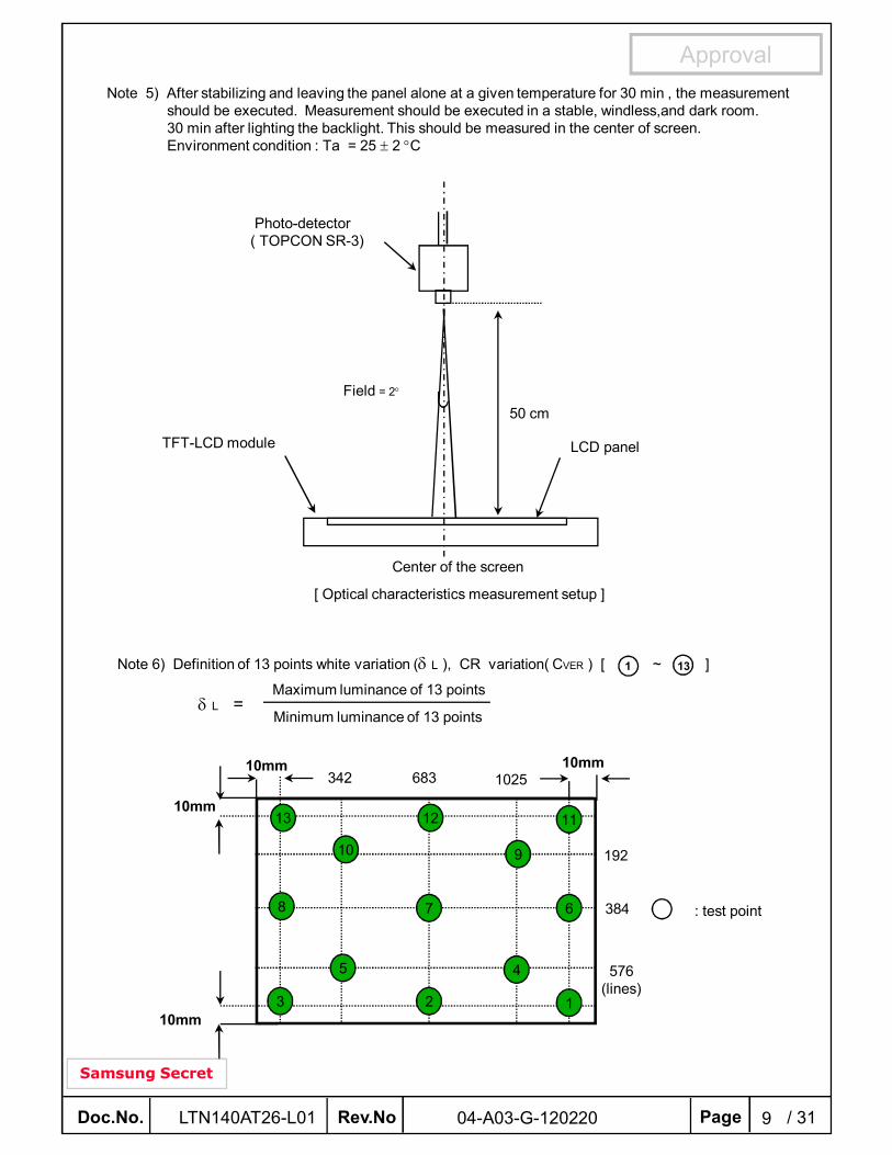
[ Optical characteristics measurement setup ]
Center of the screen
TFT-LCD module LCD panel
Photo-detector( TOPCON SR-3)
50 cm Field = 2
Note 5) After stabilizing and leaving the panel alone at a given temperature for 30 min , the measurement should be executed. Measurement should be executed in a stable, windless,and dark room.30 min after lighting the backlight. This should be measured in the center of screen. Environment condition : Ta = 25 2 C
Maximum luminance of 13 points
Minimum luminance of 13 points
: test point
342 683 1025
192
384
576(lines)
10mm
10mm
10mm 10mm
4
2
5
3
68
10 9
13 12 11
1
7
Note 6) Definition of 13 points white variation ( L ), CR variation( CVER ) [ ~ ]1 13
L =

Doc.No. Rev.No Page / 31LTN140AT26-L01 1004-A03-G-120220
Samsung Secret
Approval3. ELECTRICAL CHARACTERISTICS
3.1 TFT LCD MODULE
Note (1) Display data pins and timing signal pins should be connected.( GND = 0V )(2) fV = 60Hz, fDCLK = 75.17MHZ, VDD = 3.3V , DC Current.(3) Power dissipation pattern
*a) White Pattern *b) Mosaic Pattern
Display Brightest Gray Level
Display Darkest Gray Level
VIEW AREA
Ta= 25 2C
Item Symbol Min. Typ. Max. Unit Note
Voltage of Power Supply VDD 3.0 3.3 3.6 V
Differential InputVoltage for LVDS
Receiver Threshold
High VIH - - +100 mV VCM = +1.2V
Low VIL -100 - - mV
Vsync Frequency
60HzHsync Freq FH - 47.4 - KHz
Main Freq FDCLK - 75.17 - MHz
50HzHsync Freq FH - 39.5 - KHz
Main Freq FDCLK - 62.65 - MHz
40HzHsync Freq FH - 31.6 - KHz
Main Freq FDCLK - 50.12 - MHz
Rush Current IRUSH - - 1.5 A (4)
Current of Power Supply
White
IDD
- 210 - mA (2),(3)*a
Mosaic - 210 240 mA (2),(3)*b
WinXPPattern - 250 - mA (2),(3)*c
MaxPattern - 335 350 mA (2),(3)*d

Doc.No. Rev.No Page / 31LTN140AT26-L01 1104-A03-G-120220
Samsung Secret
Approval
*d) 1dot Vertical stripe pattern
4) Rush current measurement condition
VDD rising time is 470us
3.3V
GND
0.9VDD
0.1VDD
470us
3.3V
12V
VDD ( LCD INPUT)
CONTROL SIGNAL(HIGH to LOW)
M22SK1399
M12SK1059
R2
1K
C2
10000pFC31uF
R3
47K
R147K
FUSE C11uF
R G B R G B R G B R G
G B R G B R G B R G
R G B R G B R G B R G
G B R G B R G B R GR
R
*c) WinXP Pattern

Doc.No. Rev.No Page / 31LTN140AT26-L01 1204-A03-G-120220
Samsung Secret
Approval
3.2 Back light unit
Ta= 25 2 C
Item Symbol Min. Typ. Max. Unit Note
LED Forward Current IF - 23 - mA
LED Forward Voltage VF 3.0 3.2 3.4 V IF=23mA
LED Array Voltage VP - 32 - V VF X 10 LEDs
Power Consumption P - 2.6 2.8 W IF X VF X 30LEDs
Operating Life Time Hr 10,000 - - Hr (1)
Note (1) Life time (Hr) of LEDs can be defined as the time in which it continues to operate under thecondition Ta= 25 2 C and DC = (23) mA until one of the following event occurs.
- When the brightness becomes 50% or lower than the original.
3.3 LED Driver
- LED Driver Manufacturer : RICHTEK , LED qty.: 3X 10 = 30 EA
Item Symbol Min. Typ. Max. Unit Note
Input Voltage Vin 7 12 21 V
PWM Duty
D2 1 - 100 %PWM frequency
(0.12~1khz)
D2 5 - 100 %PWM frequency
(1~10Khz)
D2 10 - 100 %PWM frequency
(10~30Khz)
PWM Frequency FPWM 0.1 20 KHz

Doc.No. Rev.No Page / 31LTN140AT26-L01 1304-A03-G-120220
Samsung Secret
Approval4. BLOCK DIAGRAM
4.1 TFT LCD Module
4.2 LED Connection and Placement4.2 LED Connection and Placement
Converter
LVDS Input/RSDS OutputTiming Controller
14.0” HDTFT-LCD Panel
SourceDriver
ICDC-DC GammaGenerator
Input Connector
LVDS
Gate PulseGenerator
SOURCE PCB
RSDS
EDIDEEPROM
I2 C bus
VCOMGenerator
Gate IC
Mini LVDS
Control SignalVCOMGammaDVDDAVDDVon/Voff
Video Signal

Doc.No. Rev.No Page / 31LTN140AT26-L01 1404-A03-G-120220
Samsung Secret
Approval5. INPUT TERMINAL PIN ASSIGNMENT
5.1. Input Signal & Power (LVDS, Connector : IPEX 20455-040E )
Pin Symbol Function
1 NC No Connection (Reserved for supplier)
2~3 VDD Logic power 3.3V (Panel logic, BL logic)
4 VEDID EDID 3.3V power
5 NC no connect
6 CLK_EDID EDID clock
7 DATA_EDID EDID data
8 RXin0- - LVDS differential data (R0-R5, G0)
9 RXin0+ + LVDS differential data (R0-R5, G0)
10 GND Ground
11 RXin1- - LVDS differential data (G1-G5, B0-B1)
12 RXn1+ + LVDS differential data (G1-G5, B0-B1)
13 GND Ground
14 RXin2- - LVDS differential data (B2-B5,HS,VS, DE)
15 RXn2+ + LVDS differential data (B2-B5,HS,VS, DE)
16 GND Ground
17 ClkIN- - LVDS differential clock input
18 ClkIN+ + LVDS differential clock input
19 GND Ground
20~21 NC No Connection
22 GND Ground
23~24 NC No Connection
25 GND Ground
26~27 NC No Connection
28 GND Ground
29~30 NC No Connection
31~33 VBL- LED Ground
34 NC No Connection
35 S_PWM System PWM Signal Input
36 LED_EN BL On/Off (On: 2.0~3.3V, Off: 0~0.8V)
37 NC no connect
38~40 VBL+ LED Power Supply 7V-21V

Doc.No. Rev.No Page / 31LTN140AT26-L01 1504-A03-G-120220
Samsung Secret
Approval5.2 LVDS Interface
Note : The LCD Module uses a 100ohm resistor between positive and negative lines of each receiver input.
LVDS InterfaceI-PEX, 20455-40E
Pin No. Name RGB Signal Pin No. Name RGB Signal
51 TxIN0 R0 14 TxIN14 G5
52 TxIN1 R1 15 TxIN15 B0
54 TxIN2 R2 19 TxIN18 B1
55 TxIN3 R3 20 TxIN19 B2
56 TxIN4 R4 22 TxIN20 B3
3 TxIN6 R5 23 TxIN21 B4
4 TxIN7 G0 24 TxIN22 B5
6 TxIN8 G1 27 TxIN24 Hsync
7 TxIN9 G2 28 TxIN25 Vsync
11 TxIN12 G3 30 TxIN26 DE
12 TxIN13 G4 31 TxCLKIN Clock
Graphics controller18-bit
DS90CF383 Integrated ICRED0RED1RED2RED3RED4RED5
GREEN0
Hsync
Enable
GREEN1GREEN2GREEN3GREEN4GREEN5
BLUE0BLUE1BLUE2BLUE3BLUE4BLUE5
Vsync
CLOCK
5152545556346711121415192022232427283031
48
47
46
45
42
41
40
39
8
9
11
12
14
15
17
18
RxIN0-
RxIN0+
RxIN1-
RxIN1+
RxIN2-
RxIN2+
RxCLKIN-
RxCLKIN+
TxOUT0-
TxOUT0+
TxOUT1-
TxOUT1+
TxOUT2-
TxOUT2+
TxCLKOUT-
TxCLKOUT+
100
100
100
100

Doc.No. Rev.No Page / 31LTN140AT26-L01 1604-A03-G-120220
Samsung Secret
Approval
5.3 Timing Diagrams of LVDS For Transmission
LVDS Receiver : Integrated T-CON
RxOUT20 RxOUT19 RxOUT17RxOUT18 RxOUT16 RxOUT15 RxOUT14
RxOUT13 RxOUT12 RxOUT10RxOUT11 RxOUT9 RxOUT8 RxOUT7
RxOUT6 RxOUT5 RxOUT3RxOUT4 RxOUT2 RxOUT1 RxOUT0
T
T/7
Vsync B2Hsync B5 B3B4
G4B1 G5B0 G3 G2 G1
G0 R4R5 R2 R1 R0
TxCLK OUT
RxCLK IN
Rx IN1
RxIN0
Rx IN2
DE
R3

Doc.No. Rev.No Page / 31LTN140AT26-L01 1704-A03-G-120220
Samsung Secret
Approval5.5 Input Signals, Basic Display Colors and Gray Scale of Each Color
Note 1) Definition of gray : Rn: Red gray, Gn: Green gray, Bn: Blue gray (n=gray level)
Note 2)Input signal: 0 =Low level voltage, 1=High level voltage
Color Display
Data Signal GrayScaleLevel
Red Green Blue
R0 R1 R2 R3 R4 R5 G0 G1 G2 G3 G4 G5 B0 B1 B2 B3 45 B5
BasicColors
Black 0 0 0 0 0 0 0 0 0 0 0 0 0 0 0 0 0 0 -
Blue 0 0 0 0 0 0 0 0 0 0 0 0 1 1 1 1 1 1 -
Green 0 0 0 0 0 0 1 1 1 1 1 1 0 0 0 0 0 0 -
Cyan 0 0 0 0 0 0 1 1 1 1 1 1 1 1 1 1 1 1 -
Red 1 1 1 1 1 1 0 0 0 0 0 0 0 0 0 0 0 0 -
Magenta 1 1 1 1 1 1 0 0 0 0 0 0 1 1 1 1 1 1 -
Yellow 1 1 1 1 1 1 1 1 1 1 1 1 0 0 0 0 0 0 -
White 1 1 1 1 1 1 1 1 1 1 1 1 1 1 1 1 1 1 -
GrayScale
OfRed
Black 0 0 0 0 0 0 0 0 0 0 0 0 0 0 0 0 0 0 R0
Dark 1 0 0 0 0 0 0 0 0 0 0 0 0 0 0 0 0 0 R1
0 1 0 0 0 0 0 0 0 0 0 0 0 0 0 0 0 0 R2
: : : : : : : : : : : : : : : : : : :R3R60
: : : : : : : : : : : : : : : : : : :
1 0 1 1 1 1 0 0 0 0 0 0 0 0 0 0 0 0 R61
Light 0 1 1 1 1 1 0 0 0 0 0 0 0 0 0 0 0 0 R62
Red 1 1 1 1 1 1 0 0 0 0 0 0 0 0 0 0 0 0 R63
GrayScale
OfGreen
Black 0 0 0 0 0 0 0 0 0 0 0 0 0 0 0 0 0 0 G0
Dark 0 0 0 0 0 0 1 0 0 0 0 0 0 0 0 0 0 0 G1
0 0 0 0 0 0 0 1 0 0 0 0 0 0 0 0 0 0 G2
: : : : : : : : : : : : : : : : : : :G3G60
: : : : : : : : : : : : : : : : : : :
0 0 0 0 0 0 1 0 1 1 1 1 0 0 0 0 0 0 G61
Light 0 0 0 0 0 0 0 1 1 1 1 1 0 0 0 0 0 0 G62
Green 0 0 0 0 0 0 1 1 1 1 1 1 0 0 0 0 0 0 G63
GrayScale
OfBlue
Black 0 0 0 0 0 0 0 0 0 0 0 0 0 0 0 0 0 0 B0
Dark 0 0 0 0 0 0 0 0 0 0 0 0 1 0 0 0 0 0 B1
0 0 0 0 0 0 0 0 0 0 0 0 0 1 0 0 0 0 B2
: : : : : : : : : : : : : : : : : : :B3B60
: : : : : : : : : : : : : : : : : : :
0 0 0 0 0 0 0 0 0 0 0 0 1 0 1 1 1 1 B61
Light 0 0 0 0 0 0 0 0 0 0 0 0 0 1 1 1 1 1 B62
Blue 0 0 0 0 0 0 0 0 0 0 0 0 1 1 1 1 1 1 B63

Doc.No. Rev.No Page / 31LTN140AT26-L01 1804-A03-G-120220
Samsung Secret
Approval5.6 Pixel Format in the display
R G B R G B
1
R G B R G B R G B R G B
R G B R G B
LTN140AT26-L01 Panel
Line 1
Line 768
1366
Doc.No. Rev.No Page / 31LTN140AT26-L01 1904-A03-G-120220
Samsung Secret
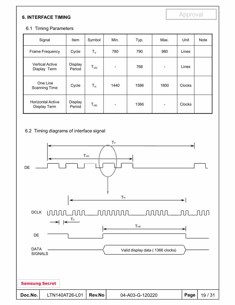
Approval6. INTERFACE TIMING
6.1 Timing Parameters
Signal Item Symbol Min. Typ. Max. Unit Note
Frame Frequency Cycle TV 780 790 980 Lines
Vertical ActiveDisplay Term
Display Period TVD - 768 - Lines
One LineScanning Time Cycle TH 1440 1586 1800 Clocks
Horizontal ActiveDisplay Term
Display Period THD - 1366 - Clocks
6.2 Timing diagrams of interface signal
TVD
TV
DE
TH
TC
THD
Valid display data ( 1366 clocks)
DCLK
DE
DATASIGNALS
Doc.No. Rev.No Page / 31LTN140AT26-L01 2004-A03-G-120220
Samsung Secret
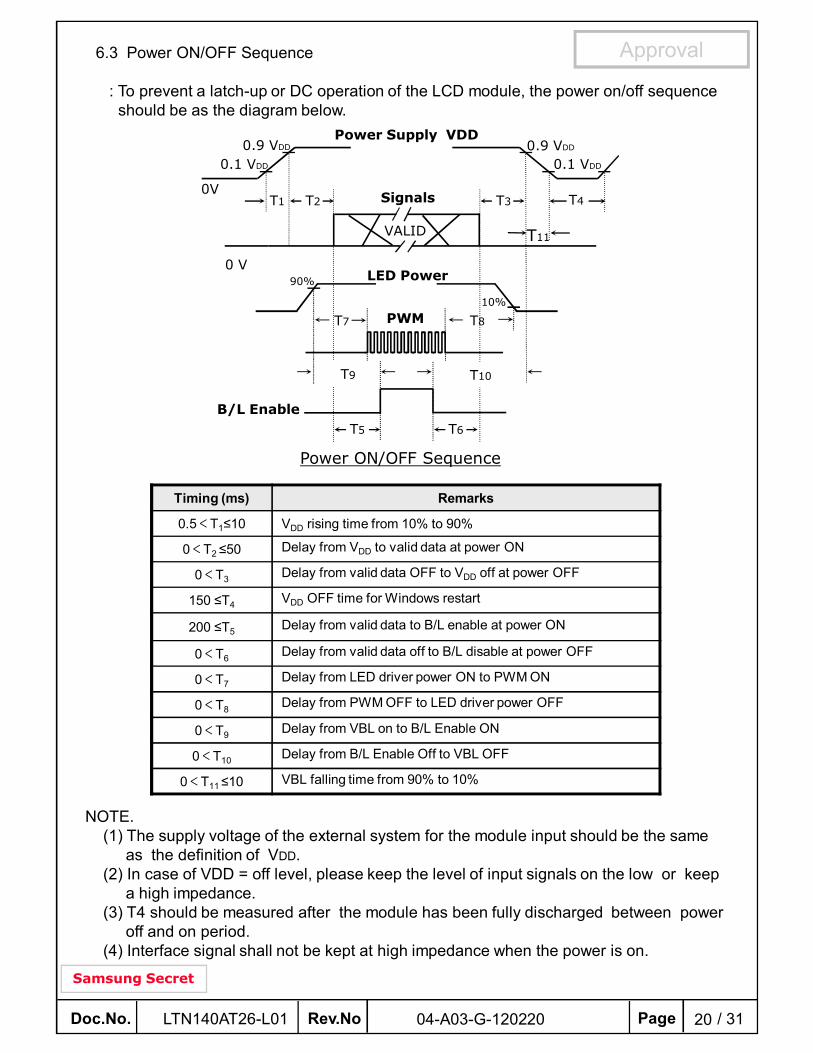
Approval6.3 Power ON/OFF Sequence
: To prevent a latch-up or DC operation of the LCD module, the power on/off sequence should be as the diagram below.
NOTE. (1) The supply voltage of the external system for the module input should be the same
as the definition of VDD.(2) In case of VDD = off level, please keep the level of input signals on the low or keep
a high impedance. (3) T4 should be measured after the module has been fully discharged between power
off and on period. (4) Interface signal shall not be kept at high impedance when the power is on.
Power ON/OFF Sequence
0 V
0.9 VDD 0.9 VDD
0V
VALID
T4
0.1 VDD 0.1 VDD
T6
B/L EnableT5
PWM
Power Supply VDD
Signals
LED Power90%
10%
T7 T8
T2 T3T1
Timing (ms) Remarks
0.5<T1≤10 VDD rising time from 10% to 90%
0<T2 ≤50 Delay from VDD to valid data at power ON
0<T3 Delay from valid data OFF to VDD off at power OFF
150 ≤T4 VDD OFF time for Windows restart
200 ≤T5 Delay from valid data to B/L enable at power ON
0<T6 Delay from valid data off to B/L disable at power OFF
0<T7 Delay from LED driver power ON to PWM ON
0<T8 Delay from PWM OFF to LED driver power OFF
0<T9 Delay from VBL on to B/L Enable ON
0<T10 Delay from B/L Enable Off to VBL OFF
0<T11 ≤10 VBL falling time from 90% to 10%
T11
T9 T10

Doc.No. Rev.No Page / 31LTN140AT26-L01 2104-A03-G-120220
Samsung Secret
Approval7. Mechanical Outline Dimension
[ Refer to the next page ]

Doc.No. Rev.No Page / 31LTN140AT26-L01 2204-A03-G-120220
Samsung Secret
Approval
This page will be replaced with the outline drawing after producing PDF file.
Doc.No. Rev.No Page / 31LTN140AT26-L01 2304-A03-G-120220
Samsung Secret
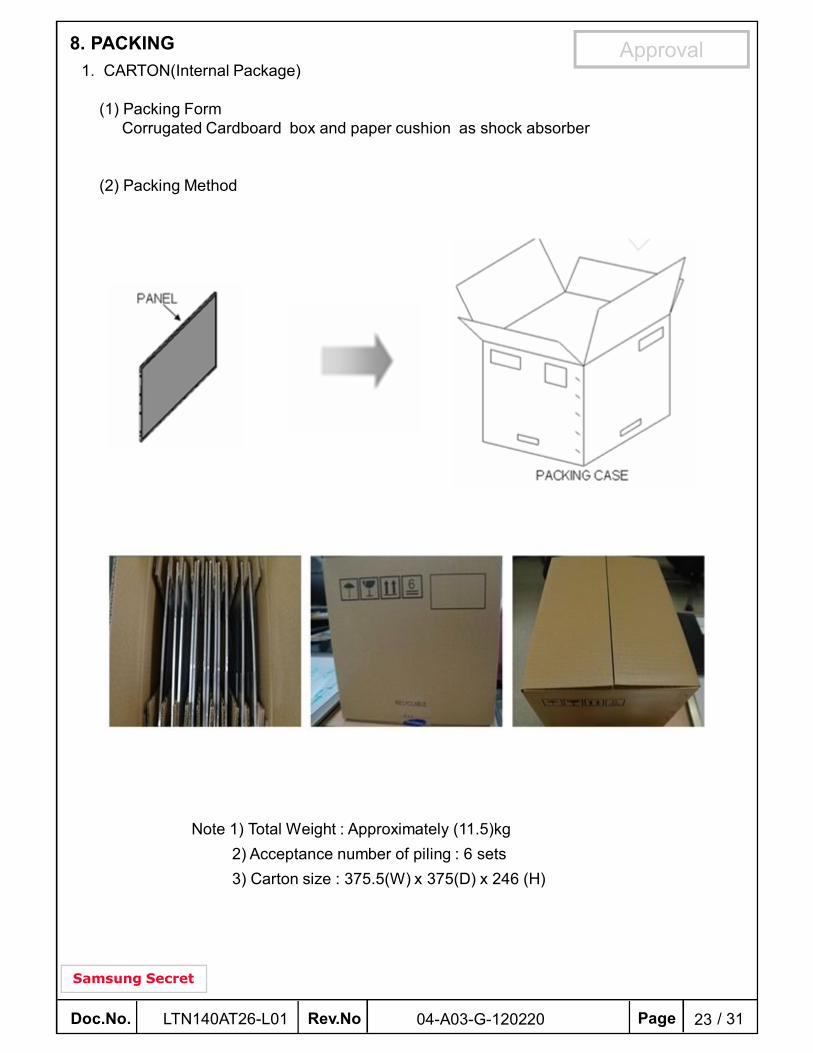
Approval8. PACKING1. CARTON(Internal Package)
(1) Packing FormCorrugated Cardboard box and paper cushion as shock absorber
(2) Packing Method
Note 1) Total Weight : Approximately (11.5)kg2) Acceptance number of piling : 6 sets3) Carton size : 375.5(W) x 375(D) x 246 (H)

Doc.No. Rev.No Page / 31LTN140AT26-L01 2404-A03-G-120220
Samsung Secret
Approval(3) Packing MaterialNo Part name Quantity
1 Static electric protective sack 30 EA
2Packing case (Inner box)
included shock absorber1 set
3 Pictorial marking 2
4 Carton 1 set

Doc.No. Rev.No Page / 31LTN140AT26-L01 2504-A03-G-120220
Samsung Secret
Approval9. Product Markings and Others
(5) Product Label Definition - SESL
A nameplate bearing followed by is affixed to a shipped product at thespecified location on each product.
(1)Parts number : LTN140AT26-L01(2)Revision : Three letters(3)Control code : One letter(4)Lot number : X X X X XXX XX X XXX
SEC Revision CodeCell IDGlass IDLot IDMonthYearDeviceLine
TFT-LCD Product name : LTN140AT26USP code : XXXXXXXXXXXXX
Lot number : XXXXXXXXXXX Revision Code : L01Inspected work week :1204 (2012 Year, the 04th week)P/N : 0B50871EC NO : -FRU : 04W4023Header Code : 1ZKJE
: 11SXXXXXXXX1ZKJE XXXXXX XXX
Lenovo P/N (7 digits)
Lenovo H/C (5 digits)Serial No (6 digits)
YMM
Lenovo Barcode
40 mm
80 mm
LTN140AT26
XXXXXXXXXX L01P / N 0B50871 EC NO FRU 04W4023
xxxxxxxxxxx1ZKJExxxxxx xxx
1204
MADE IN CHINA
D

Doc.No. Rev.No Page / 31LTN140AT26-L01 2604-A03-G-120220
Samsung Secret
Approval
(6) Packing small box attach
DEVICE : LTN140AT26TYPE : L01QUANTITY : 30 PCS
CO6040001
Doc.No. Rev.No Page / 31LTN140AT26-L01 2704-A03-G-120220
Samsung Secret
Approval10. GENERAL PRECAUTIONS
1. Handling
(a) When the module is assembled, It should be attached to the system firmly using every mounting holes. Be careful not to twist and bend the modules.
(b) Refrain from strong mechanical shock and / or any force to the module. In addition to damage, this may cause improper operation or damage to the module and back-light.
(c) Note that polarizers are very fragile and could be easily damaged. Do not press or scratchthe surface harder than a HB pencil lead.
(d) Wipe off water droplets or oil immediately. If you leave the droplets for a long time,Staining and discoloration may occur.
(e) If the surface of the polarizer is dirty, clean it using some absorbent cotton or soft cloth.
(f) The desirable cleaners are water, IPA (Isoprophyl Alcohol) or Hexane.Do not use Ketone type materials(ex. Acetone), Ethyl alcohol, Toluene, Ethyl acid or Methyl chloride. It might permanent damage to the polarizer due to chemical reaction.
(g) If the liquid crystal material leaks from the panel, it should be kept away from the eyes or mouth . In case of contact with hands, legs or clothes, it must be washed away thoroughlywith soap.
(h) Protect the module from static , it may cause damage to the C-MOS Gate Array IC.
(i) Use fingerstalls with soft gloves in order to keep display clean during the incoming inspection and assembly process.
(j) Do not disassemble the module.
(k) Do not pull or fold the lamp wire.
(l) Do not adjust the variable resistor which is located on the back side.
(m) Protection film for polarizer on the module shall be slowly peeled off just before use sothat the electrostatic charge can be minimized.
(n) Pins of I/F connector shall not be touched directly with bare hands.
Doc.No. Rev.No Page / 31LTN140AT26-L01 2804-A03-G-120220
Samsung Secret
Approval2. STORAGE
(a) Do not leave the module in high temperature, and high humidity for a long time.It is highly recommended to store the module with temperature from 0 to 35 C and relative humidity of less than 70%.
(b) Do not store the TFT-LCD module in direct sunlight.
(c) The module shall be stored in a dark place. It is prohibited to apply sunlight or fluorescentlight during the store.
3. OPERATION
(a) Do not connect,disconnect the module in the “ Power On” condition.
(b) Power supply should always be turned on/off by following item 6.3 “ Power on/off sequence “.
(c) Module has high frequency circuits. Sufficient suppression to the electromagnetic interference shall be done by system manufacturers. Grounding and shielding methodsmay be important to minimize the interference.
(d) The FPC cable between the LED chips and its converter power supply shall be aminimized length and be connected directly . The longer cable between the back-lightand the converter may cause lower luminance of light source (LED).
(e) The standard limited warranty is only applicable when the module is used for general notebook applications. If used for purposes other than as specified, SEC is not to be held reliable for the defective operations. It is strongly recommended to contact SEC to find out fitness for a particular purpose.
4. OTHERS
(a) Ultra-violet ray filter is necessary for outdoor operation.
(b) Avoid condensation of water. It may result in improper operation or disconnection of electrode.
(c) Do not exceed the absolute maximum rating value. ( the supply voltage variation, input voltage variation, variation in part contents and environmental temperature, so on) Otherwise the module may be damaged.
(d) If the module displays the same pattern continuously for a long period of time,it can bethe situation when the image “sticks” to the screen.
(e) This module has its circuitry PCB’s on the rear side and should be handled carefully in order not to be stressed.
Doc.No. Rev.No Page / 31LTN140AT26-L01 2904-A03-G-120220
Samsung Secret
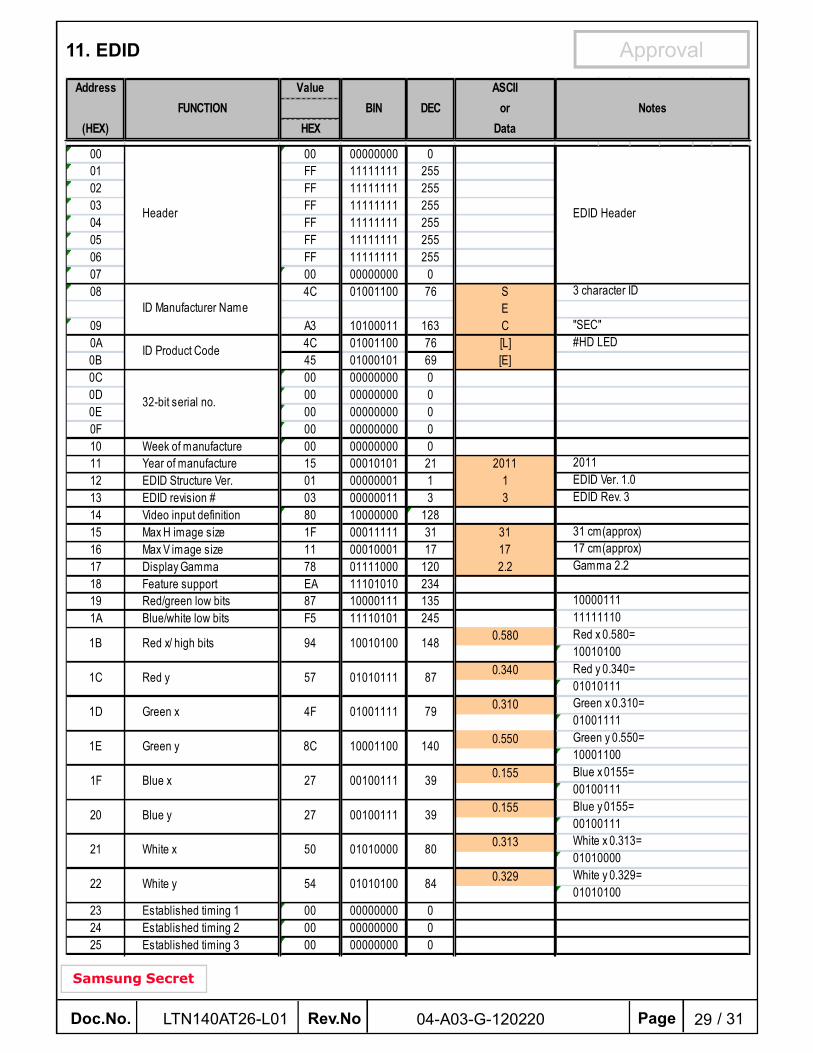
Approval11. EDID
Address Value ASCIIor
(HEX) HEX Data
00 00 00000000 001 FF 11111111 25502 FF 11111111 25503 FF 11111111 25504 FF 11111111 25505 FF 11111111 25506 FF 11111111 25507 00 00000000 008 4C 01001100 76 S
E09 A3 10100011 163 C0A 4C 01001100 76 [L]0B 45 01000101 69 [E]0C 00 00000000 00D 00 00000000 00E 00 00000000 00F 00 00000000 010 Week of manufacture 00 00000000 011 Year of manufacture 15 00010101 21 201112 EDID Structure Ver. 01 00000001 1 113 EDID revision # 03 00000011 3 314 Video input definition 80 10000000 12815 Max H image size 1F 00011111 31 3116 Max V image size 11 00010001 17 1717 Display Gamma 78 01111000 120 2.218 Feature support EA 11101010 23419 Red/green low bits 87 10000111 1351A Blue/white low bits F5 11110101 245
0.580
0.340
0.310
0.550
0.155
0.155
0.313
0.329
23 Established timing 1 00 00000000 024 Established timing 2 00 00000000 025 Established timing 3 00 00000000 0
White y 0.329=01010100
00100111Blue y 0155=00100111
01010000White x 0.313=
1000011111111110Red x 0.580=
Red y 0.340=
Blue x 0155=
31 cm(approx)17 cm(approx)Gamma 2.2
2011EDID Ver. 1.0EDID Rev. 3
21 White x 50 01010000
22 White y 54 01010100
20 Blue y 27 00100111
1F Blue x 27 00100111
1E Green y 8C 10001100
1D Green x 4F 01001111
1C Red y 57 01010111
ID Manufacturer Name
ID Product Code
32-bit serial no.
EDID Header
3 character ID
"SEC"#HD LED
DEC Notes
148
87
79
14010001100
39
FUNCTION BIN
Header
1B Red x/ high bits 94 10010100
39
80
84
10010100
01010111Green x 0.310=01001111Green y 0.550=

Doc.No. Rev.No Page / 31LTN140AT26-L01 3004-A03-G-120220
Samsung Secret
Approval26 01 00000001 127 01 00000001 128 01 00000001 129 01 00000001 12A 01 00000001 12B 01 00000001 12C 01 00000001 12D 01 00000001 12E 01 00000001 12F 01 00000001 130 01 00000001 131 01 00000001 132 01 00000001 133 01 00000001 134 01 00000001 135 01 00000001 136 5D 01011101 93 75.1737 1D 00011101 2938 56 01010110 86 136639 DC 11011100 220 2203A 50 01010000 803B 00 00000000 0 7683C 16 00010110 22 223D 30 00110000 483E 30 00110000 48 483F 20 00100000 32 32
25
42 35 00110101 53 30943 AE 10101110 174 17444 10 00010000 1645 00 00000000 046 00 00000000 047 19 00011001 2548 00 00000000 049 00 00000000 04A 00 00000000 04B 0F 00001111 154C 00 00000000 04D 00 00000000 04E 00 00000000 04F 00 00000000 050 00 00000000 051 00 00000000 052 00 00000000 053 00 00000000 054 00 00000000 0
55 25 00100101 37
56 D9 11011001 217
57 06 00000110 6
58 6A 01101010 106
59 00 00000000 0
Value=Tvbpmin / 2
Value=Thbpmin /2
2bit : 2bit :2bit :2bit
Module revision
Hor blanking=220pixels4bit : 4bit
H sync. Width=32 pixelsV sync. Offset=2 linesV sync. Width=5 lines
not used
not used
not used
Value=VSPWmax /2
Thpmin=value*2 + HA pixelclksThpmax=value*2 + HA pixelclksTvpmin=value*2 + VA lines
H image size= 309 mm(approx)V image size = 174 mm(approx)
No Horizontal Border
Value=Thbpmax /2Value=VSPWmin /2
Tvpmax=value*2 + VA lines
Value=HSPWmin / 2Value=HSPWmax / 2
Detailed timing/monitor
Detailed timing/monitor
descriptor #2
Vertcal active=768 linesVertical blanking=22 lines4bit : 4bit
Manufacturer Specified (Timing)
Value=Tvbpmax / 2
No Vertical Border
Hor sync. Offset=48 pixels
Main clock= 75.17 MHz (@60Hz)
Hor active=683*2 pixels
40 descriptor #1 25 00100101 37
41 00 00000000 0
Standard timing #7
Standard timing #8
not used
not used
Standard timing #5
Standard timing #6
not used
not used
Standard timing #3
Standard timing #4 not used
Standard timing #1
Standard timing #2

Doc.No. Rev.No Page / 31LTN140AT26-L01 3104-A03-G-120220
Samsung Secret
Approval5A 00 00000000 05B 00 00000000 05C 00 00000000 05D FE 11111110 2545E 00 00000000 05F 53 01010011 83 [S]60 41 01000001 65 [A]61 4D 01001101 77 [M]62 53 01010011 83 [S]63 55 01010101 85 [U]64 4E 01001110 78 [N]65 47 01000111 71 [G]66 0A 00001010 10 [ ]̂67 20 00100000 32 [ ]68 4C 01001100 7669 A3 10100011 1636A 41 01000001 65 [A]
6B 54 01010100 84 [T]6C 00 00000000 06D 00 00000000 06E 00 00000000 06F FE 11111110 25470 00 00000000 071 4C 01001100 76 [L]72 54 01010100 84 [T]73 4E 01001110 78 [N]74 31 00110001 49 [1]75 34 00110100 52 [4]76 30 00110000 48 [0]77 41 01000001 65 [A]78 54 01010100 84 [T]79 32 00110010 50 [2]7A 36 00110110 54 [6]7B 4C 01001100 76 [L]7C 30 00110000 48 [0]7D 31 00110001 49 [1]7E Extension Flag 00 00000000 07F Checksum E2 11100010 226
Monitor Name Tag (ASCII)
ASCII Data String Tag
supplier ID "SEC"
Product code "AT"
(Hex, LSB firs t)
descriptor #4Detailed timing/monitor
Detailed timing/monitordescriptor #3