Embed Size (px)
Citation preview

M-Band J Series CMPA (VZM-6993J4) 04/00 TD-82 1
Technical Description
M-Band J Series Compact Medium Power AmplifierVZM-6993J4
811 Hansen WayPalo Alto, CA 94303
Phone: (650) 846-3700Fax: (650) 424-1744
INTRODUCTION
This document provides a detailed technical description of the Communications & Power Industries, Inc. (CPI),VZM-6993J4 Series M-band Compact Medium Power Amplifier (CMPA), a 250 Watt medium power travelingwave tube amplifier designed specifically for broadband microwave applications such as EMC and generalpurpose testing. The J Series CMPA is compact and lightweight and employs a state-of-the-art widebandTraveling Wave Tube (TWT). The TWT permits continuous, efficient instantaneous operation across the entire 8.0to 18.0 GHz frequency. The J Series CMPA also incorporates the use of a microprocessor control system,thereby simplifying interfacing with remote control and monitor facilities. Both RS 422/485 and IEEE-488interface ports are included as standard features. Microwave features include a Solid State Intermediate PowerAmplifier (SSIPA), microprocessor controlled RF gain control and soft-fail VSWR protection. The J SeriesCMPA also features active power factor correction (0.95 min.) which allows the unit to meet the total harmonicdistortion requirement of EN60555-2. It is also designed to meet EN61010 safety and 89/336/EEC electromag-netic compatibility requirements.
The VZM-6993J4 Series CMPA along with the VZS/C-6963J2 (2.0 – 8.0 GHz) and the VZL-6943J2 (1.0 –2.5 GHz), cover the full 1.0 – 18.0 GHz in three units. The J Series CMPA family is a member of a comprehensiveline of communication amplifiers including TWT Low Power Amplifiers (LPAs), Medium Power Amplifiers(MPAs), High Power TWT Amplifiers (HPAs) and High Power Klystron Amplifiers (KPAs) designed specificallyfor service in commercial satellite earth stations operating in standard SATCOM frequency bands.
CPI (formerly Varian Electron Device Group) has been active in the design and manufacture of microwave poweramplifiers and related products for more than 30 years. CPI Satcom Division (formerly Varian MEP), wasorganized in the mid-1970s to bring together under a single business center the strengths of existing groupsinvolved with commercial Satcom and Industrial power amplifiers.
Today, CPI Satcom Division has provided thousands of fully integrated satellite uplink power amplifiers in the S,C, Ku, X, M, DBS and Ka- band frequency ranges to worldwide users and has become the leading supplier of thisclass of products.
M-Band J Series CMPA

M-Band J Series CMPA (VZM-6993J4) 04/00 TD-82 2
EQUIPMENT DESCRIPTION
General
The VZM-6993J4 CMPA (Figure 1) is packaged in a5.25 inch tall slide-mounted drawer suitable for stan-dard 19-inch rack mounting. This enclosed assemblyhouses both the RF and power supply sections of theamplifier. The RF section includes the TWT, solid stateintermediate power amplifier (IPA), optional Input Iso-lator, input RF Gain control, RF detectors and outputdirectional couplers for monitoring and protection. Thepower supply section includes the power factor cor-rection, power processor, and high voltage regulationcircuitry. It also contains all monitor, control and pro-tection circuits necessary to permit safe, efficient andreliable operation of the J Series CMPA .
The VZM-6993J4 CMPA is protected from opera-tional damage caused by abnormal AC, DC, RF faultsor insufficient cooling. The amplifier will automaticallyrecycle itself after a prime power interruption or tran-sient fault condition.
Personnel safety is of utmost importance and is safe-guarded by proper grounding and by access interlocksand shields, which prevent physical entry into the highvoltage sections.
The front panel of the unit serves as the primary userinterface housing all monitor and control functions in-cluding a type N RF connector to sample and measureoutput RF power. Opening the small access door onthe front panel allows easy access to configuration DIPswitches that can be set during installation, up/downbuttons that permit setting high and low alarm trippoints (such as Low RF), and a set of detail fault LEDsto help troubleshoot during operation.
Principal functions are also brought to the four userinterface connectors located on the rear panel for re-mote monitor and control. Control, fault and monitor-ing functions are available via: the IEEE-488 interfacedesigned to interface directly with a computer, an RS-422/485 port to be used when the optional CPI remotecontrol panel is purchased, a separate switching portfor use with switching/power combining subsystems,and a user interlock port for use when interfacing otherequipment or controls with the J Series CMPA.
Digital attenuation allows for RF drive attenuation ad-justment via the remote interface ports thereby enhanc-ing remote monitor and control capabilities.
REFLECTED RF (W)
ATTENUA TOR SETTING (V)
RF OUTPUT (W)
RF OUTPUT (dB m)
HTD
TX SELECTSTANDBY
TRANS MIT
FAULT
RECYCLEDFAULT
LO CA L
RE S E T
HELIX VOLTAGE (kV)
HELIX CURRENT (mA)
C I F
RE M OT E
S T A NDB Y
T RA NS MI T
LOCAL
REMOTE
CIF
ME TER S ELE CT
RF S A M P
RF S E T TIN G
0
1
Figure 1. J Series CMPA

M-Band J Series CMPA (VZM-6993J4) 04/00 TD-82 3
To expedite field maintenance procedures, the VZM-6993J4 CMPA utilizes a modular design approachconsisting of Line Replaceable Units (LRUs), whichpermit service personnel to maintain the J SeriesCMPA in the field without need of returning the entireunit to the depot or factory. Comprehensive built-in-test (BIT) sequences and diagnostic procedures allowfield personnel to localize the fault to the individualLRU, make the necessary replacement and return theamplifier to service with a minimum of operationaldowntime.
The overall amplifier enclosure measures approxi-mately 19" (w) x 5.25" (h) x 24" (d), plus air ductadapters, and weighs approximately 70 lbs. The TWTAmplifier can be installed in a 1:1, 1:2 or 1:3 autoswitching, or power combined configuration as neededby end user mission.
RF Subsystem
A conservative field-proven approach is utilized in the JSeries CMPA RF subsystem. The RF block diagram(Figure 2) identifies all major circuit elements for thistechnical description.
A low level RF input signal is applied to the J SeriesCMPA via a type N connector located at the rear ofthe enclosure. The input VSWR is less than 2.5:1 andcan be further reduced with the optional input isolatorto a level of 1.5:1 or less back to the source. The RF
input is then routed to the SSIPA which includes aninternal variable RF attenuator. The attenuator, has auser control range of 20 dB plus an additional 15 dB ofrange for the soft-fail VSWR feature. The IPA isdesigned to be transparent to final amplifier RF param-eters. The output of the SSIPA is then fed to the inputof the TWT. The SSIPA and TWT provide a com-bined subsystem gain of at least 54 dB at rated power.The overall J Series CMPA gain is specified to bestable within ±0.25 dB/24 hours with ±10% line volt-age variations.
The primary microwave power amplifier in the VZM-6993J4 is the CPI VTM-6294M4 TWT. The TWT isan efficient design featuring conduction cooling, dualdepressed collectors, and Periodic Permanent Magnet(PPM) focused helix design. It is lightweight and de-signed especially for harsh environments in a widevariety of applications over temperatures of –40°C to+110 °C.
The output waveguide coupler assembly interfaces tothe TWT and provides both a forward and reversesample of the RF output.
This coupler is a broadwidth design to assure goodflatness and directivity over the full 8-18 GHz band.The two port directional coupler provides one re-flected power port coupled via a detector to the RF
Figure 2. J Series CMPA RF Diagram
INPUTISOLATOR
*SOLID STATEAMPLIFIER
*Contains integral RF Gain Control
TO RFMONITORCCA, A7
RF MONITOR(TYPE N FEMALE)
RF OUTPUT(WRD 750)
RF INPUT(TYPE N FEMALE)
TWTDUAL DIRECTIONAL COUPLER

M-Band J Series CMPA (VZM-6993J4) 04/00 TD-82 4
power monitor assembly for reverse power protectionand a forward power sample. The forward sample isfurther split by a coaxial coupler into two samples, onefor the user to monitor forward RF power via a type Nconnector on the front panel and one for use by thefront panel forward power metering circuit which usesa thermoelectric power monitor to process the RFsignal. The RF sample port is nominally –57 dB, andpermits independent monitoring of J Series CMPAoutput power levels through the use of an externalspectrum analyzer or portable power meter. Low andhigh RF power alarms are user settable via the frontpanel access door.
High reflected RF soft-fail protection circuitry is stan-dard and reflected power information is sent to thefront panel for display.
The output and reflected power level readouts are alsoavailable for remote monitoring via the optional CPIremote panel or the computer interface RS 422/485
and IEEE-488 ports located on the rear panel. RFdrive is adjustable via these ports as well. The standardRF output interface to connect the J Series CMPA tothe external waveguide run is a WRD-750 waveguideflange.
Soft-Fail Reflected Power Protection
Reflected power is monitored in part to protect theTWT. The M-band J Series CMPA employs a Soft-Fail protection feature to allow operation even underoutput mismatch conditions that cause excessive re-flected power. To protect the TWT, this feature ac-tively reduces the RF output power to keep the re-flected power below the reflected power trip point.With the factory setting of 25 W trip level, the actualreflected power will be actively limited during opera-tion to around 22 W by the CMPA controller byreducing the RF gain. Once the reflected power dropsbelow 17 W, soft-fail operation will end and normaloperation is restored. In the soft-fail mode the Re-flected RF meter LED will flash.
Figure 3. Power Supply Block Diagram
EMIFilter
ACInput Circuit
Breaker Fans
208-240 VAC
Power FactorCorrection
ModulePower
Processor
375 VDC
Flash RAM Programming
Switching I/F
Serial Remote I/F(RS 422/485)
IEEE-488 Remote I/F
User Interlocks
Control&
Display
Micro-controller
RF Metering& Faults
Control&
DC Power
Monitor
Gain Control
HVModule
Helix
CathodeColl. 1
Coll. 2
RF Subsystem
TWT
Linearizer
(optional)
DCPower
SSIPA
RF Monitor
DCPower
Heater

M-Band J Series CMPA (VZM-6993J4) 04/00 TD-82 5
Power Supply Subsystem
Overview
The power supply portion of the J Series CMPAprovides all of the internal voltages necessary to oper-ate the TWT, RF driver (SSIPA), forced air coolingsystem and auxiliary circuits for control, monitoring andprotection. Only the AC input power and RF inputdrive power is required for operation. The travellingwave tube derives its operation from four DC powersupplies: a filament heater low voltage supply, a helixhigh voltage supply and two collector high voltagesupplies.
The power supply design utilized in the VZM-6993J4Series is of the switch mode power conditioner(SMPC) type which has an excellent reputation forreliability and stability. An added advantage of theSMPC approach over outdated linear power suppliesis its intrinsic high efficiency and safe operation. Bylimiting the amount of the instantaneous stored energyin the power supply, the risk of permanent damage tothe J Series CMPA due to abnormal or transient con-ditions is avoided. The momentary level of stored en-ergy (measured in joules) is well below the maximumlimit of energy that the tube can safely dissipate duringany condition. A simplified block diagram of the powersupply is shown in Figure 3. The principal circuit mod-ules are discussed in the following paragraphs.
Power Factor Correction Module
Input primary power (single phase, 110-240 VAC)flows via a EMI filter and the main circuit breaker toboth the cooling system power supply and the PowerFactor Correction Module. This module provides aregulated 375 VDC to the Power Processor and al-lows the CMPA to meet the requirements ofEN60555-2 regarding total harmonic distortion. In theevent of a failure of this module, a DC bus fault flag issent to the micro-controller for proper fault handlingand display via the detail fault LEDs located throughthe front panel access door.
Power Processor Module
The power processor circuits provide the necessaryline and load regulation of the input 375 volt DC bus,which is converted via a switch regulator and bridgecircuit to a nominal 200 volt, 21 kHz to drive the highvoltage module. A sample of the helix high voltageoutput is returned to the switch regulator for errorfeedback correction and sends a pulse-width modu-lated signal through an optical isolator to the switchingtransistors. This approach allows careful regulation ofthe TWT helix and collector voltages and protects bothsupplies from over voltage/under voltage or short cir-cuit conditions. Low voltage outputs are also producedby this assembly (+/-15 VDC and 16 VAC) which areused to operate various internal circuit functions as wellas provide power for the RF monitor circuit, micro-controller assembly, front panel display, and SSIPA.Internal sensors provide the necessary over-currentprotection functions for these supplies.
High Voltage Module
The high voltage module provides the following keypower supply functions: regulated TWT heater supply,regulated TWT high voltage helix and collector sup-plies, helix supply current/voltage monitoring and faultprotection. The high voltage module contains the trans-formers, rectifiers, filters and voltage/current sense re-sistors for critical TWT voltages. The incoming 200volt, 21 kHz signal is applied to the primary of a multi-section high voltage transformer which provides all ofthe high voltage levels necessary to operate the travel-ing wave tube. Since the helix and collectors share thesame transformer and regulator, the high voltage circuitdesign establishes the collector voltages at 50% (col-lector #1) and 32% (collector #2) depression belowthe helix voltage. This relationship permits optimumefficiency and substantial energy savings while extend-ing the useful life of the TWT. A separate step-downtransformer with rectifier and filter network is em-ployed to provide the heater voltage.
M-Band J Series CMPA (VZM-6993J4) 04/00 TD-82 6
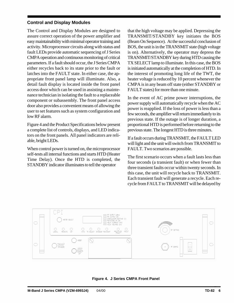
Control and Display Modules
The Control and Display Modules are designed toassure correct operation of the power amplifier andeasy maintainability with minimal operator training andactivity. Microprocessor circuits along with status andfault LEDs provide automatic sequencing of J SeriesCMPA operation and continuous monitoring of criticalparameters. If a fault should occur, the J Series CMPAeither recycles back to its state prior to the fault orlatches into the FAULT state. In either case, the ap-propriate front panel lamp will illuminate. Also, adetail fault display is located inside the front panelaccess door which can be used in assisting a mainte-nance technician in isolating the fault to a replaceablecomponent or subassembly. The front panel accessdoor also provides a convenient means of allowing theuser to set features such as system configuration andlow RF alarm.
Figure 4 and the Product Specifications below presenta complete list of controls, displays, and LED indica-tors on the front panels. All panel indicators are reli-able, bright LEDs.
When control power is turned on, the microprocessorself-tests all internal functions and starts HTD (HeaterTime Delay). Once the HTD is completed, theSTANDBY indicator illuminates to tell the operator
that the high voltage may be applied. Depressing theTRANSMIT/STANDBY key initiates the BOS(Beam On Sequence). At the successful conclusion ofBOS, the unit is in the TRANSMIT state (high voltageis on). Alternatively, the operator may depress theTRANSMIT/STANDBY key during HTD causing theTX SELECT lamp to illuminate. In this case, the BOSis initiated automatically at the completion of HTD. Inthe interest of promoting long life of the TWT, theheater voltage is reduced by 10 percent whenever theCMPA is in any beam off state (either STANDBY orFAULT states) for more than one minute.
In the event of AC prime power interruptions, thepower supply will automatically recycle when the ACpower is reapplied. If the loss of power is less than afew seconds, the amplifier will return immediately to itsprevious state. If the outage is of longer duration, aproportional HTD is performed before returning to theprevious state. The longest HTD is three minutes.
If a fault occurs during TRANSMIT, the FAULT LEDwill light and the unit will switch from TRANSMIT toFAULT. Two scenarios are possible.
The first scenario occurs when a fault lasts less thanfour seconds (a transient fault) or when fewer thanthree transient faults occur within twenty seconds. Inthis case, the unit will recycle back to TRANSMIT.Each transient fault will generate a recycle. Each re-cycle from FAULT to TRANSMIT will be delayed by
Figure 4. J Series CMPA Front Panel

M-Band J Series CMPA (VZM-6993J4) 04/00 TD-82 7
one second. After the unit successfully recycles toTRANSMIT, the RECYCLED FAULT LED willflash until the user presses RESET. Each fault causes adetail fault LED to illuminate behind the front panelaccess door. This LED will remain lit until the RESETbutton is pressed or power is cycled.
The second scenario occurs when a fault lasts longerthan four seconds or when at least three faults occurwithin twenty seconds. In this case the unit will belatched into FAULT and the FAULT LED will flash.To reset the unit for normal operation, clear the sourceof the fault. Then, press RESET. If the fault was suc-cessfully cleared, the FAULT LED will extinguish andthe unit will be in STANDBY. Press TRANSMIT/STANDBY to resume transmitting.
In either case, the pertinent fault remains displayed onthe detail fault display inside the front panel accessdoor until hitting the RESET button. This allows theable user or technician the ability to identify individualfaults to a specific module or subassembly.
Power Monitor Circuits
The RF power monitor assembly receives signals fromthe forward and reflected power RF detectors for usein fault/alarm sensing and forward power metering. Theforward power detector is a thermo-electric powermonitor, which provides optimum flatness over thefrequency band. The reflected RF fault sensor/recyclecircuit protects the TWT against excessive reflectedpower due to abnormal waveguide or antenna condi-tions. Additionally, the forward power metering circuitmeasures both continuous wave (CW) and peak RFsignals. Also included is a forward power low RFalarm circuit which compares the output power with auser-settable low RF set point and triggers an alarm,should output power fall below this level.
Mechanical Design
General
The VZM-6993J4 Series CMPA is packaged in astandard rack mounted drawer measuring 19" wide by5.25" high and 24" deep (plus connectors, fan and airduct adapters). The unit is cooled via a forced aircooling system consisting of two axial fans, an air filterand an exhaust duct. Allowances are made for 0.10"H20 drop due to customer ducting losses.
LRU Philosophy
The CMPA utilizes a modular design approach incor-porating LRUs for ease of maintainability in the field.The maintenance concept employed in the VZM-6993J4 Series CMPA is to localize a malfunction orcircuit failure down to the level of an LRU, extract theLRU and replace with an equivalent part provided inthe spares kit. This procedure can be completed in thefield without resorting to the costly practice of returningthe entire J Series CMPA to the depot for servicing.The philosophy is to configure the LRUs as buildingblocks with a specific function that can be monitoredby sensors and fault indicators on a real-time basis.

M-Band J Series CMPA (VZM-6993J4) 04/00 TD-82 8
PRODUCT SPECIFICATIONS
The following specification limits and characteristics apply to the 250 W VZM-6993J4 Series unless otherwisespecified.
ElectricalFrequency 8.0 to 18.0 GHz
Output Power•TWT 54.0 dBm min. (250 watts)•flange 53.5 dBm min. (225 watts)
Instantaneous Bandwidth 10.0 GHz
Gain•at rated power 53.5 dB min.•small signal 55.5 dB min.
RF Attenuator Adjust Range 0 to 20 dB
Output Power Resolution within ±0.2 dB max.
Gain Stability•at constant drive & temperature ±0.25 dB/24 hr max.(after 30 min. warm-up)•over temperature, constant drive
Small Signal Gain Variation(across the 10.0 GHz band) 12 dB pk-pk, typ. (See Figure 1)
Input VSWR 2.5:1 max., 1.5:1 max with optional input isolator
Output VSWR 2.5:1 typical
Load VSWR•full spec compliance 1.5 max.•operation without damage any value•continuous operation 2.0:1 max. for full output power, any value under
soft-fail modeResidual AM
•below 10 kHz -50 dBc•10 to 500 kHz -20 (1.3+log F kHz) dBc•above 500 kHz -85 dBc
Phase Noise Meets IESS-308/309 phase noise profilewith 3 dB margin
AM/PM Conversion 1.5°/dB typical. for a single carrier at 8 dB below rated power
Harmonic Output -3 dBc typical at lower band edge, decreasing to –15 dBc typical at upper band edge
Noise and Spurious (at rated gain) -50 dBc excluding harmonics
Noise Figure 15 dB max.

M-Band J Series CMPA (VZM-6993J4) 04/00 TD-82 9
Electrical (Cont)
Intermodulation -24 dBc typical with two equal carriers attotal power level 7dB below rated single carrieroutput.
Primary Power 220-240 ±10%, single phase47-63 Hz
Power Factor 0.95 min. (meets requirements of EN60555-2,total harmonic distortion)
Power Consumption 1.4 kVA typ.1.5 kVA max.
Inrush Current 200% max.
Environmental
Ambient Temperature•operating -10° to +40°C•non-operating -40° to +70°C
Relative Humidity 95% non-condensing
Altitude•operating 10,000 ft., w/ standard adiabatic derating of
2°C/1,000 ft.•non-operating 40,000 ft.
Shock and Vibration As normally encountered in a protectedengineering laboratory environment, and inshipping via commercial carriers in CPIprovided containers.
M-Band J Series CMPA (VZM-6993J4) 04/00 TD-82 10
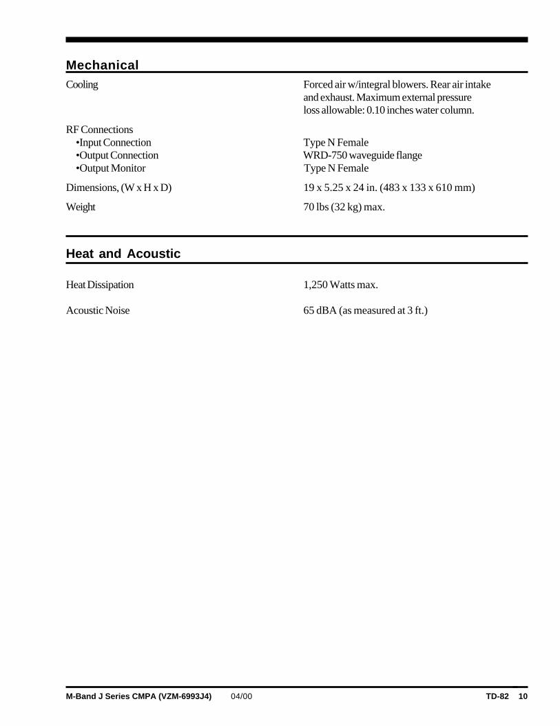
MechanicalCooling Forced air w/integral blowers. Rear air intake
and exhaust. Maximum external pressureloss allowable: 0.10 inches water column.
RF Connections•Input Connection Type N Female•Output Connection WRD-750 waveguide flange•Output Monitor Type N Female
Dimensions, (W x H x D) 19 x 5.25 x 24 in. (483 x 133 x 610 mm)
Weight 70 lbs (32 kg) max.
Heat and Acoustic
Heat Dissipation 1,250 Watts max.
Acoustic Noise 65 dBA (as measured at 3 ft.)

M-Band J Series CMPA (VZM-6993J4) 04/00 TD-82 11
MONITORS AND CONTROLS - FRONT PANEL
Control Functions Main Power On/OffTX (Transmit) SelectTransmit/Standby (Beam on/off)RF drive adjustLocal/Remote/Computer (CIF) SelectIndicator TestFault ResetFault SettingsSerial Port Settings
Monitoring RF Output Sample Port (-57 dB nominal, Type N female)RF Reflected Power (Watts)Helix Current (mA)Helix Voltage (kV)Elapsed time meter, hours
Controls/Status Display Power OnHeater Time Delay (HTD) 180sec nominal; proportionalTX (Transmit) SelectStandbyTransmit (Beam On)Local/Remote/CIFMeter Select
Fault/Alarm Display Recycled Fault (Automatic fault recycle 3 times)FaultLow RF (with Forward Power Metering Option)High Reflected PowerInterlocks Open (power supply temp. or amplifier cover)Helix Over-currentHelix VoltagePower Supply ArcDC Bus FaultTWT Over-temperatureFault Log
Metering RF Output Power (Watts and dBm)Resolution: greater of 1W or 0.1dBAccuracy: +/-10% at 12 GHz factory calibration+/-2.5 dB over frequency(Calibration can be set at individual freq. by user)

M-Band J Series CMPA (VZM-6993J4) 04/00 TD-82 12
REMOTE CONTROL INTERFACES
Standard interfaces RS-422/485 (4 wire) and IEEE-488 listener/talker
Control Functions TX (Transmit) SelectTransmit/Standby (Beam on/off)Set RF AttenuatorSet RF Output PowerRemote/Computer (CIF) Select*Inhibit RFFault ResetSet RF Alarm and Fault Trip Points
Monitoring RF Reflected Power (Watts)Helix Current (mA)Helix Voltage (kV)RF Attenuator setting (V)
Metering RF Output Power (Watts or dBm)Resolution: greater of 1W or 0.1dB
Status Display Heater Time Delay (HTD) 180sec nominal; proportionalTX (Transmit) SelectStandbyTransmit (Beam On)Local/Remote (serial)/Remote (GPIB)
Fault/Alarm Display Recycled Fault (Automatic fault recycle 3 times)FaultLow RF or High RFHigh Reflected PowerInterlocks Open (power supply temp. or amplifier cover)Helix Over-currentHelix VoltagePower Supply ArcDC Bus FaultTWT Over-temperatureSoft-Fail activeSSIPA Over-current
*Available on RS422/485 port and Local Front Panel Only

M-Band J Series CMPA (VZM-6993J4) 04/00 TD-82 13
OPTIONS & FEATURES
Options & Compatibility Primary PowerRemote Control PanelRedundant and Power Combined SubsystemsInput isolator (Input VSWR is reduced to 1.5:1 max).
Features Soft-Fail Reflected Power ProtectionIntegral microprocessor controlled RF Gain StandardForward Power Metering StandardDesigned to meet EN61010/EN60555-2 Safety/ Harmonic standards as well as 89/336 EEC/ EMC StandardsFilament voltage reduction of 10% in standbyIEEE-488 and RS-422/485 (4-wire) remote interfaces standardAuto Fault RecycleUtilizes high efficiency dual depressed collector traveling wave tubeInternal test points for ease of maintenance, plus BIT diagnostic front panel LEDsMTTR < 1 hr
Also available in 250 W L and S/C Band models
Characteristics and performance limits are based on current data and are subject to change without notice. Please contactCPI Satcom Division before using this information for system design.

M-Band J Series CMPA (VZM-6993J4) 04/00 TD-82 14
ACCESSORIESSeveral optional accessory items have been designedfor use with the CPI 250 W J Series M-band CMPAs.Brief descriptions of the items now available are givenon the following paragraphs.
Phase Combining
The Phase Combiner consists of a coaxial input dividernetwork and phase shifter and an output waveguidecombining system.
The combiner assembly is packaged in a 19-inch rack-mountable enclosure.
The combiner assembly can also be supplied mountedin the rack/cabinet which houses the two J SeriesCMPAs to provide an integrated power-combinedCMPA system.
Remote Control Panels
The Remote Control/Monitor panel is a rack-mount-able unit 5.25 inches high that provides an output RFpower meter and all of the remote controls and indica-tors listed in this brochure. The panel requires a sourceof AC power and it does not include the interconnectcable from the J Series CMPA. The cable requires 4conductors plus a shield and practical wire sizes limitthe length to about 1100 feet (335 meters).
The J-Rack remote RS422/485 interface is used withthe Remote Control Panel.

M-Band J Series CMPA (VZM-6993J4) 04/00 TD-82 15
Typical Performance Data
Listed below are some typical test data taken on a standard production unit. This data is followedby several graphs in Figures 5.
1. Rated Power and Gain
Frequency (GHz) Saturated P out (dBm) Gain at 224 W (dB) RF Sample Port (dB)8.0 54.7 56.2 55.89.0 55.3 60.6 56.410.0 54.5 61.5 56.611.0 54.8 64.4 57.512.0 54.8 67.6 58.113.0 55.0 68.0 58.314.0 54.6 65.8 57.715.0 54.4 63.6 57.816.0 54.8 62.6 58.017.0 59.3 61.3 58.318.0 54.9 55.9 57.7
2. Small Signal Gain 60.4 dB min. (See Figure 5)
3. SSG Variation 11.0 dB p-p max. (See Figure 5)
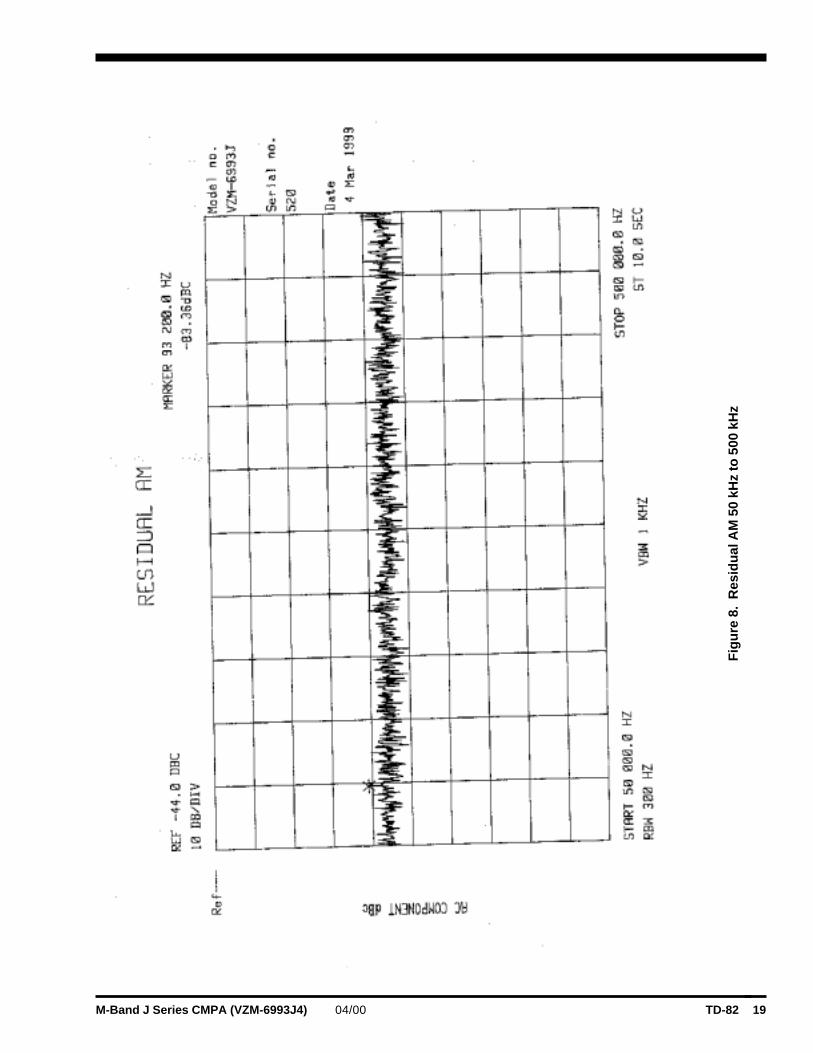
4. Residual AM See Figures 6, 7 and 8
0 10 kHz -82 dBc at 980 Hz10-50 kHz -85 dBc at 41.6 kHz50-500 kHz -83.0 dBc at 92.7 kHz
5. Group Delay See Figure 9

M-Band J Series CMPA (VZM-6993J4) 04/00 TD-82 16
Fig
ure
5.
Sm
all S
ign
al G
ain
Res
po
nse

M-Band J Series CMPA (VZM-6993J4) 04/00 TD-82 17
Fig
ure
6.
Res
idu
al A
M 0
kH
z to
10
kHz

M-Band J Series CMPA (VZM-6993J4) 04/00 TD-82 18
Fig
ure
7.
Res
idu
al A
M 1
0 kH
z to
50
kHz
M-Band J Series CMPA (VZM-6993J4) 04/00 TD-82 19
Fig
ure
8.
Res
idu
al A
M 5
0 kH
z to
500
kH
z

M-Band J Series CMPA (VZM-6993J4) 04/00 TD-82 20
Fig
ure
9.
Gro
up
Del
ay

M-Band J Series CMPA (VZM-6993J4) 04/00 TD-82 21
SUPPORT SERVICES
Documentation
CPI Satcom Division provides a standard commercialdocumentation package for all products. The standardpackage for satellite communications power amplifiersincludes a detailed installation and operation manual,outline and interface drawings and Test PerformanceSheet (TPS).
The O & I manual provides instruction for unpackingand installation, initial set-up, calibration, normal op-eration, and scheduled maintenance of the equipment.The manual includes a block diagram, outline and inter-connect drawing. Outline and interface drawings pro-vide dimensions and the location and size of mountingholes, duct work, and waveguide, so that site prepara-tion can be accomplished prior to receipt of the equip-ment.
The TPS outlines the factory tests performed, andlimits established. Space is provided for recording andcertifying the test results, consolidating all related infor-mation in one document.
An optional comprehensive Service manual is alsoavailable. The Service manual provides detailed theoryof operation, instructions for troubleshooting and main-tenance, adjustments and calibration of the equipment.The manual includes schematic diagrams, block dia-grams, and wiring information sufficient for use bymaintenance personnel.
On request, a spare parts documentation package isavailable. This consists of a commercial recommendedspare parts list to support the equipment for a one-to-two year period of operation.
Training
CPI Satcom Division is prepared to conduct trainingcourses covering the installation, operation and mainte-nance of its equipment. The training course on highpower amplifiers consists of lectures using training ma-terial, such as technical manuals and drawings, plusactual operation and adjustments demonstrated on theequipment.
Small training groups (up to five students) assure thecustomer that each student has an opportunity to par-ticipate fully in demonstration activities. Courses maybe conducted at the CPI factory or on-site. Courseduration varies from two days to one or two weeks,depending on the scope of work agreed upon and theskill level of the students.
Field Service
The product support activity of CPI includes a staff ofexperienced, professional service technicians to assistusers in maintaining full performance from their CPIpower amplifiers. A telephone “hot line” permits ac-cess to one of these technicians on a 24-hour per daybasis. Operational problems often can be diagnosed,corrective action prescribed, and normal operationrestored through telephone consultation. When calledfor, however, the service technicians are prepared togive on-site assistance.
Product Support carries an inventory of spare partsthat can be made ready for shipment within 24 hours.Coupled with a dedicated dial-in telephone line, thisservice is effective in aiding users to restore equipmentto operational status with minimum downtime. Techni-cal assistance and factory approved replacement partsare also available at strategically located Regional Ser-vice Centers in the U.S.A., Europe, and the PacificRim.