Embed Size (px)
Citation preview

----- CONFIDENTIAL ------------------------------------------ CONFIDENTIAL ----MACINTOSH HARDWARE MEMORY MAP
----- CONFIDENTIAL
Page 1
Page 2
Page 3
Page 4
Page 5 Page 6
Page 7
Page 8
Page 9
Page 10
Page 11
Page 12
Page 13
Page 14
Page 15
Page 16
Page 17
Page 18
Page 19
Burrell Smith and Brian Howard
13 April 1983 ------------------------------------------ CONFIDENTIAL -----
1. INTRODUCTION
2. MEMORY MAP ON POWER-UP (OVERLAY =
3. NORMAL MEMORY MAP (OVERLAY = 0)
4. RAM 4.1 Address Decoding to Activate RAMs 4.2 Some Useful RAM Addresses 4.3 More Detailed Map of RAM 4.4 Hardware Exception Vectors
5. ROM 5.1 Address Decoding to Activate ROMs 5.2 Useful ROM Addresses
6. SCC 6.1 Address Decoding to Activate SCC 6.2 Further SCC Address Decoding 6.3 Some Useful SCC Addresses
7. IWM 7.1 Address Decoding to Activate IWM 7.2 Further IWM Address Decoding 7.3 Some Useful IWM Addresses
8. VIA 8.1 Address Decoding to Activate VIA 8.2 Further VIA Address Decoding 8.3 Some Useful VIA Addresses
1)
8.4 Macintosh-Specific Information about VIA Registers 8.4.1 Port A Input, Output, and Data Direction Registers 8.4.2 Port B Input, Output, and Data Direction Registers 8.4.3 Control Registers 8.4.4' Interrupt Flag and Enable Registers
9. PHASE READ 9.1 Address Decoding to Activate PHASE READ 9.2 Further PHASE READ Address Decoding 9.3 Using PHASE READ
10. AUTO-VECTOR "READ" ADDRESSES
11. SOME USEFUL DECODING EQUATIONS

13 April 1983 Macintosh Memory Map Page 1
1. INTRODUCTION
The principle portions of Macintosh's memory consist of volatile read/write memory (RAM) and permanent read-only memory (ROM). In addition to RAM and ROM, three input/output devices are also selected using address lines, so that they appear to occupy portions of the Macintosh memory space. These devices are the 6522 Versatl~e Interface Adapter (VIA), the 8530 Serial Communications,Chip (SCC), and the disk interface chip (IWM).
When the Macintosh is first turned on, ROM appears at ehe bottom (lowest -- >-"1
addresses) portion of the memory space. This is useful for the ROM-stored software which starts the system running. Afte~·tup, the OVERLAY signal from the VIA is changed to a low (zero), mapping RAM into its normal place at the bottom of memory.
Selection of RAM, ROM, or other devices is done by from two to five of the highest-order address lines, A23-A19. The VIA and IWM also use the four address lines A12-A9 for further internal decoding and register selection, while the SCC uses the three lowest-order address lines A2-A0 for internal decoding.
In specifying "useful addresses" for most devices, unused address lines have been set high (to a one) to save a small amount of power and to improve noise immunity. Some address ranges are specified "Do Not Use" because they can select two devices simultaneously. While this does not cause any damage to the computer, data cannot be correctly transferred while these addresses are in use.

13 April 1983 Macintosh Memory Map
2. MEMORY MAP ON POWER-UP (OVERLAY = 1)
(Auto-Vector Read)
No Device Assigned
PHASE READ
VIA (A0=0)
Do Not Use (2 devices on bus)
$ FF FFFF $ FF FFF0
$ F8 0000
$ F0 0000
$ E8 0000
~ $ E0 0000
IWM (A0=1)
Do Not Use (2 devices on bus)
sec WRITE (A0=1)
Do Not Use (2 devices on bus)
sec RESET (A0=1). sec READ (A0=0 )
Do Not Use (2 devices on ~us) ,
RAM (128 K Bytes)
No Device Assigned
Duplicate 64 K ROM image
No Device Assigned
No Device Assigned
ROM (64 K Bytes)
$ D0 0000
$ e0 0000
$ B0 0000
$ A0 0000
$ 90 0000
$ 80 0000
$ 62 0000
$ 60 0000
$ 50 0000
$ 41 0000
$ 40 0000
$ 30 0000
$ 20 0000
$ 10 0000
$ 01 0000
$ 00 0000
Page 2

13 April 1983 Macintosh Memory Map
3. NORMAL MEMORY MAP (OVERLAY = 0)
(Auto-Vector Read)
No Device Assigned
PHASE READ
VIA (A0=0)
Do Not Use (2 devices on bus)
IWM (A0=1)
Do Not Use (2 devices on bus)
see WRITE (A0=1)
Do Not Use (2 devices on bus)
sec RESET (A0=1) see READ (A0=0)
Do Not Use (2 devices on bus)
No Device Assigned
Reserved (16 ROM images)
No Device Assigned
Reserved (15 ROM images)
ROM (64 K Bytes)
Reserved (31 RAM images)
RAM (128 K Bytes)
$ FF FFFF $ FF FFF0
$ F8 0000
$ F0 0000
$ E8 0000
$ E0 0000
$ D0 0000
$ e0 0000
$ B0 0000
$ A0 0000
$ 90 0000
$ 80 0000
$ 70 0000
$ 60 0000
$ 50 0000
$ 41 0000
$ 40 0000
$ 02 0000
$ 00 0000
Page 3

13 April 1983
4. RAM
Macintosh Memory Map
/W (------- RAM R/W --------) /W (A23-22 or A23-21)
/RAS (-------- /RAS ----------) /RAS /CAS0 ---) /CAS ICASI ---) ICAS
A0 (--------- RA0 ----------) A0
A7 (--------- RA7 ----------) A7
D0 •• 7 ---) D D8 •• 1S ---) D
Page 4
Q ---) RQ0 •• 7 Q ---) R08 •• 1S
Eight 64k bit DRAMs USF ••• UI2F
4.1 Address Decoding to Activate RAMs
Eight 64k bit DRAMs USG ••• U12G
Note: RAM is written when RAM R/W = 0. Ro0-RQlS are read onto the data bus when /RAM READ = 0.
When RAM Address Lines Address Addressed A23 A22 A21 A20 Range
Startup: 0 1 1 X $600000-$7FFFFF OVERLAY=1
Normal: X X $000000-$3FFFFF OVERLAY=0
(Note: X indicates "don't care": either 1 or 0)
4.2 Some Useful RAM Addresses
128K RAM Addresses
Video Screen, Page 1 Video Screen, Page 2
$000000 - $01FFFF
$01A700 (top) - $01FC7F (bottom) $012700 (top) - $017C7F (bottom)
Sound/PWM Buffer, Page 1 $01FD00 - $01FFE3 Sound/PWM Buffer, Page 2 $01A100 - $01A3E3 (Note: Sound = high bytes, PWM = low bytes)
($SS80 bytes)
($2E4 bytes)
RAM Addresses during startup (OVERLAY = 1)
Video Screen, Page 1, during startup (OVERLAY = 1)
$600000 - $61FFFF
$61A700 - $61FC7F
13 April 1983 Macintosh Memory Map
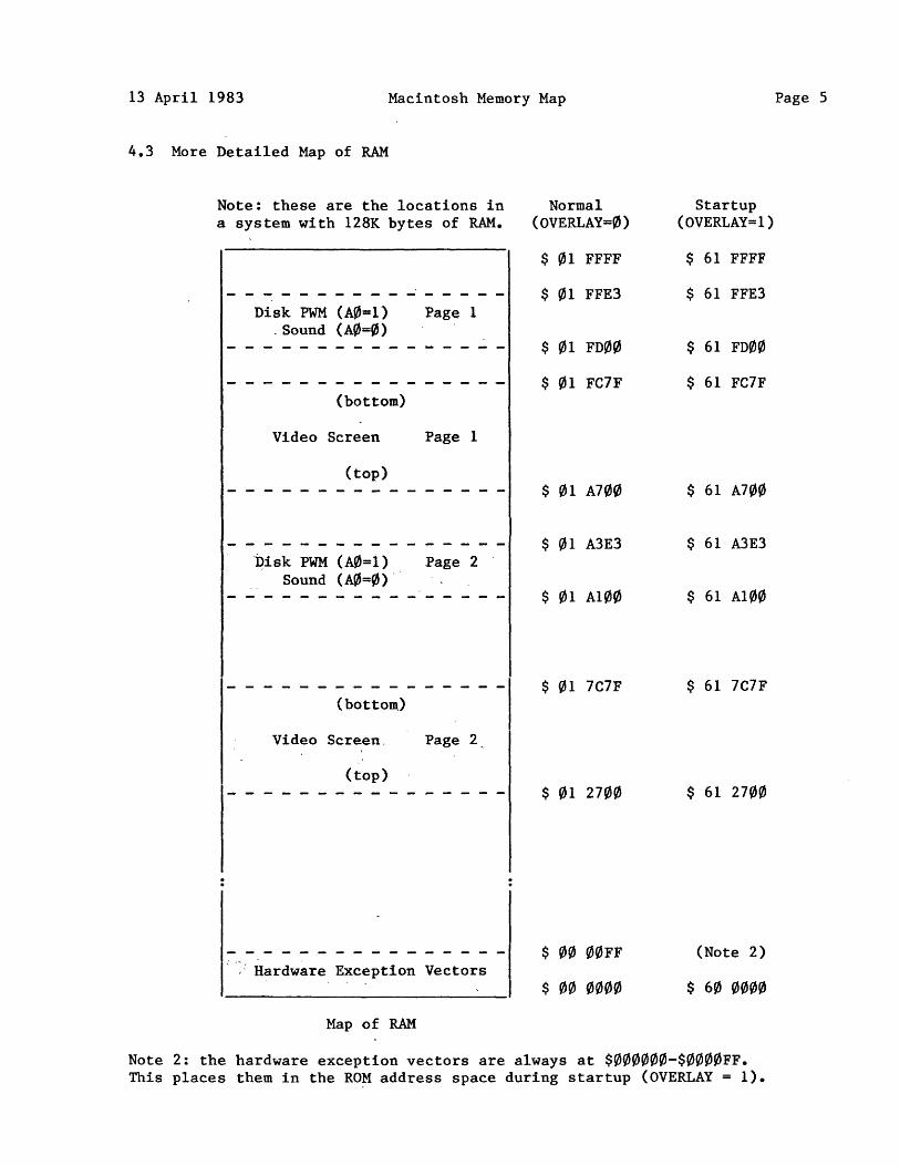
4.3 More Detailed Map of RAM
Note: these are the locations in Normal a system with 128K bytes of RAM. (OVERLAY=0)
Disk PWM (A0=1) -Sound (A0=1/J )
(bottom)
Video Screen
(top)
Page 1
Page 1
TIisk PWM (A0=i) Page 2 Sound (A'/J=0)"
- - - - - - - - - - - - - -(bottom)
Video Screen, Page 2
(top) - - - - - - - - - - - - - -
'~" Hardware Exception Vectors
Map of RAM
$ 01 FFFF
$ 01 FFE3
$ 01 FD00
$ 01 FC7F
$ 01 A71/J0
$ 01 A3E3
$ 01 A100
$ 01 7C7F
$ 01 2700
$ 00 00FF
$ 00 0000
Startup (OVERLAY=I)
$ 61 FFFF
$ 61 FFE3
$ 61 FD00
$ 61 FC7F
$ 61 A700
$ 61 A3E3
$ 61 A100
$ 61 7C7F
$ 61 2700
(Note 2)
$ 60 0000
Note 2: the hardware exception vectors are always at $000000-$0000FF. This places them in the ROM address space during startup (OVERLAY = 1).
Page 5

13 April 1983 Macintosh Memory Map
4.4 Hardware Exception Vectors (in RAM if OVERLAY = 0)
Reset: Initial SSP
Reset: Initial PC
Bus Error
Address Error
Illegal Instruction
Divide by Zero
CHK Instruction
TRAPV Instruction
Privilege Violation
Trace
Line 1010 Emulator
Line 1111 Emulator
I (Unassigned: Reserved) ---------------------------------
Uninitialized Interrupt
(Unassigned: Reserved)
Spurious Interrupt
VIA Interrupt Auto-Vector
SCC Interrupt Auto-Vector
VIA+SCC (temp.) Auto-Vector
Interrupt Switch Auto-Vector
Int.Sw.+VIA Auto-Vector
Int.Sw.+SCC Auto-Vector
Int.Sw.+VIA+SCC Auto-Vector
TRAP Instruction Vectors
(Unassigned: Reserved)
$00 0000
$00 0004
$00 0008
$00 000C
$00 0010
$00 0014
$00 0018
$00 001C
$00 0020
$00 0024
$00 0028
$00 002C
$00 0030 - $00 003B
$00 003C
$00 004C - $00 005F
$00 0060
$00 0064
$00 0068
$00 006C
$00 0070
$00 0074
$00 0078
$00 007C
$00 0080 - $00 00BF
$00 00c0 - $00 00FF
Page 6

13 April 1983
5. ROM
Macintosh Memory Map
ICE <----------A20-----------> ICE IOE (--------/ROMEN----------> 10E
(A23-21 or A23-22)
A0 <-----------Al-----------> A0
A15 <---------~-AI5----------> A15
00 ----> D0
07 ----> D7
Page 7
00 ----) D8
07 ---) DIS
ROM LO U8D
ROM HI U6D
5.1 Address Decoding to Activate ROMs
Note: ROM is activated whenever A20=0 and IROMEN=0.
When ROM Address Lines Address Addressed A23 A22 A21 A20 Range (Exceptions)
Startup: 1 0 X 0 $000000-$0FFFFF, OVERLAY=1 $200000-$2FFFFF
and 0 1 0 0 $400000-$4FFFFF
Normal: 0 1 X 0 $400000-$4FFFFF, OVERLAY=0 $600000-$6FFFFF
Anytime: 1 0 X 0 $800000-$8FFFFF, (Do not use: SCC is OVERLAY=X $A00000-$AFFFFF also on the bus)
and 1 1 0 0 $C00000-$CFFFFF (Do not use: IWM is also on the bus)
(Note: X indicates "don't care": either 1 or 0)
5.2 Useful ROM Addresses
Note: these addresses are for a system with 64K bytes of ROM.
Startup ROM Addresses (OVERLAY = 1)
Normal ROM Addresses
$000000 - $00FFFF or $400000 - $40FFFF (duplicate ROM image)
$400000 - $40FFFF

13 April 1983
6. SCC
/SCCEN ----) ICE (A23-22)
/SCCRD ----) /RD (A23-21)
Macintosh Memory Map Page 8
/RTSA ----) /OEBUFA I I TxDA ----) TXDA -----------) TXD+,- Serial RxDA (---- RXDA (----------- RXD+,- Channel A /LDS ----) /WR
(A0) /CTSA,/TRxCA (---- TTLHSKA (-------- HSK J2
Al ----) A/B A2 ----) D/C
/SYNCA - n.c. /DTR-REQA - n.c.
I /DCDA (---- MOUSE Xl (------- Xl Mouse
J5 PCLK,
3.7M ----) RTxCA, RTxCB
/DCDB (---- MOUSE Y1 (------- Y1
/W-REQA, /W-REQB ----) scc WT/REQ -------------) VIA's PA7
D8 (----) D0 /RTSA ----) /OEBUFB
D15 (----) D7 TxDB ----) TXDB -----------) TXD+,- Serial RxDB (---- RXDB (----------- RXD+,- Channel B
/CTSB,/TRxCB (---- TTLHSKB (-------- HSK J3 /SYNCB - n.c.
/DTR-REQB - n.c.
scc (8530) U13D
6.1 Address Decoding to Activate SCC
Device Address Lines But Do Addressed A23 A22 A21 A20 Not Use
SCC Read 1 0 0 X 1000: ROM is (/SCCEN=0, also on bus
/SCCRD=0)
SCC Write 1 1 X 10¹⁰: ROM is (/SCCEN=0, also on bus
/SCCRD=l)
(Note: X indicates "don't care": either 1 or 0)
Address Range (Exceptions)
$800000-$9FFFFF (But do not use $800000-$8FFFFF)
$A00000-$BFFFFF (But do not use $A00000-$AFFFFF)

13 April 1983 Macintosh Memory Map Page 9
6.2 Further SCC Address Decoding A2 Al A0
/LDS = 0 X X 1 /LDS = 1 X X 0
Channel A X I X Channel B X 0 X
Data Register 1 X X Control Register 0 X X
READ Byte Read:
The SCC uses the upper byte of the data bus, so use A0 = 0 for reading the SCC. This sets /LDS high and the CPU reads data from D8-DIS. A0 = 0
RESET Byte Read:
A byte access to any SCC READ address with A0 = I sets /LDS and /SCCRD both low. This resets the SCC.
A0 = I
WRITE Byte Write:
This uses a special feature of the 68000 CPU: a write to the lower byte of the data bus (A0=I) also places the same data on the upper byte of the data bus. /LDS is set low and the CPU writes the same byte of data to Df/J-D7 and to D8-DIS.
A0 = I
PHASE ADJUST Word Read or Word Write
Normal accesses to the SCC are byte accesses. A word access to the SCC adjusts the phase of the computer's high-frequency timing signals by 128 nS. See section 9.3, PHASE READ, to determine whether the timing is in phase or out of phase.
6.3 Some Useful SCC Addresses
Channel A: Write to data register $BFFFFF Read from data register $9FFFFE
Channel B: Write to data register $BFFFFD Read from data register $9FFFFC
Channel A: Write to control register specified in Write Register 0 $BFFFFB
Channel A: Read from control register specified in Write Register f/J $9FFFFA
Channel B: Write to control register specified in Write Register 0 $BFFFF9
Channel B: Read from control register specified in Write Register 0 $9FFFF8
Reset SCC $9FFFFF
Adjust timing phase: word read from $9FFFFE

13 April 1983
7. IWM
Macintosh Memory Map
IIWM ----) IDEV (A23-21)
lAS ----) 03
IRES ----) IRES
8M ----) FCLK
A9 ----) Al A10 ----) A2 All ----) A3 A12 ----) A4
D0 <----) D0
D7 <----) D7
IWM UllD
IENBL1 ----) IENBLI IENBL2 ----) IENBL2
IWRREO ----) IWR REO
WRDATA ----) WRDATA
RDDATA, SENSE <---- RD
E0 ----) PHASE0 E1 ----) PHASE1 E2 ----) PHASE2 E3 ----) PHASE3
Page 10
7.1 Address Decoding to Activate IWM
Device Address Lines Addressed A23 A22 A21 A20
IWM 1 1 0 X (/IWM=0)
(Note: X indicates "don't care":
But Do Not Use
1100: ROM is also on bus
either 1 or 0)
Address Range (Exceptions)
$c00000-$DFFFFF (But do not use $C00000-$CFFFFF)

13 April 1983 Macintosh Memory Map Page 11
7.2 Further IWM Address Decoding
7.3
These State
A12
All
A10
A9
A0 1
Some Useful IWM Addresses
These three lines select one of the eight bits in the IWM State Register.
When /DEV (/IWM) goes low, the IWM State Register bit selected by A12-A10 is set to the "value" (1 or 0) on line A9.
The rwM uses the lower byte of the data bus, so use A0 = 1 •
are addresses which use A12-A9 to set individual bits in the IWM Register.
State Register IWM Macintosh
Bit Function Address
0 Phase 0: Low $DFE1FF High $DFE3FF
1 Phase 1: Low $DFE5FF High $DFE7FF
2 Phase 2: Low $DFE9FF High $DFEBFF
3 Phase 3: Low $DFEDFF High $DFEFFF
4 Motor: Off $DFFIFF (disables all drives) On $DFF3FF (enables selected drive)
5 Select:" Drive 1 $DFF5FF (selects internal drive) Drive 2 $DFF7FF (selects external drive)
6 Disk Q6: Low $DFF9FF (called L6 in IWM document) High $DFFBFF
7 Disk Q7: Low $DFFDFF (called L7 in IWM document) High $DFFFFF

13 April 1983
8. VIA
/A20 ----) CSI /VMA ----) ICS2
(A23-2I)
A9 ----) RS0 AI0 ----) RSI All ----) RS2 AI2 ----) RS3
IRES ----) IRES
Macintosh Memory Map
PA0 ----) sv0 PAl ----) SVI PA2 ----) SV2 PA3 ----) /SND PG2 PA4 ----) OVERLAY PAS ----) SEL PA6 ----) /VID PG2 PA7 (---- /SCC WT-REQ
CAl (---- IVSYNC CA2 (---- 1 SEC CLKOUT
R/w ----) R/w PB0 (---) RTC.DATA PBl ----) RTC.CLK
E-Mu ----) Ph 2 PB2 ----) IRTC PB3 (---- IMOUSE SW PB4 (---- I·iOUSE X2
IVIA IRQ (---- IIRQ PBS (---- MOUSE Y2
D8 (----) D0
DI5 (----) D7
(Timer 2) PB6 (---- H4 (Timer 1) PB7 ----) SND RES
VIA (6522) UISD
CBl (---) KBD.SCLK CB2 (---) KBD.DATA
8.1 Address Decoding to Activate VIA
Device Address Lines But Do Addressed A23 A22 A21 A20 A19 Not Use
VIA 1 1 1 0 X 11100: PHASE (/VMA=0. READ on bus IA20=1)
(Note: X indicates "don't care": either 1 or 0)
Page 12
(Sound Volume: LSB) (Sound Volume) (Sound Volume: MSB) (0 = Sound Buffer Page 2) (1 = ROM in low-memory) (Disk Head Select) (0 = Video Page 2) (Channels A & B)
(Vertical Blanking) (I-Second Clock Int)
(Clock Data) (Clock Data Timer) (Clock Enable) (0 if switch is pressed)
(Horizontal Blanking) (Sound Reset)
(Keyboard Data Timer) (Keyboard Data)
Address Range (Exceptions)
$E00000-$EFFFFF (But do not use $E00000-$E7FFFF)

13 April 1983 Macintosh Memory Map
8.2 Further VIA Address Decoding
A12 All A10 A9
A'/1 = '/1
These four lines select one of 16 VIA registers.
The VIA uses the upper byte of the data bus, so use A'/1 = '/1 •
8.3 Some Useful VIA Addresses
Page 13
These are addresses which use A12-A9 to select individual VIA registers.
Input or Output Register A
Input or Output Register B
Data Direction Register A Data Direction Register B
Timer 1 Counter: Low Byte High Byte
Timer 1 Latch: Low Byte High Byte
Timer 2 Counter: Low Byte High Byte
Shift Register
$EFFFFE
$EFE1FE
$EFE7FE $EFE5FE
$EFE9FE $EFEBFE
$EFE9FE $EFEBFE
$EFFIFE $EFF3FE
$EFF5FE
Auxiliary Control Register $EFF7FE
Peripheral Control Register $EFF9FE
Interrupt Flag Register $EFFBFE
Interrupt Enable Register $EFFDFE
(Do NOT use 1-0 Register A with Handshake: $EFE3FE)
('/1-bits indicate inputs, while l's are outputs)
(Associated with PB7)
(Down-counter; may be associated with PB6)
(Shifts data into or out of VIA on CB2, clocked by Ph 2, Timer 2, or CB1)
13 April 1983 Macintosh Memory Map Page 14
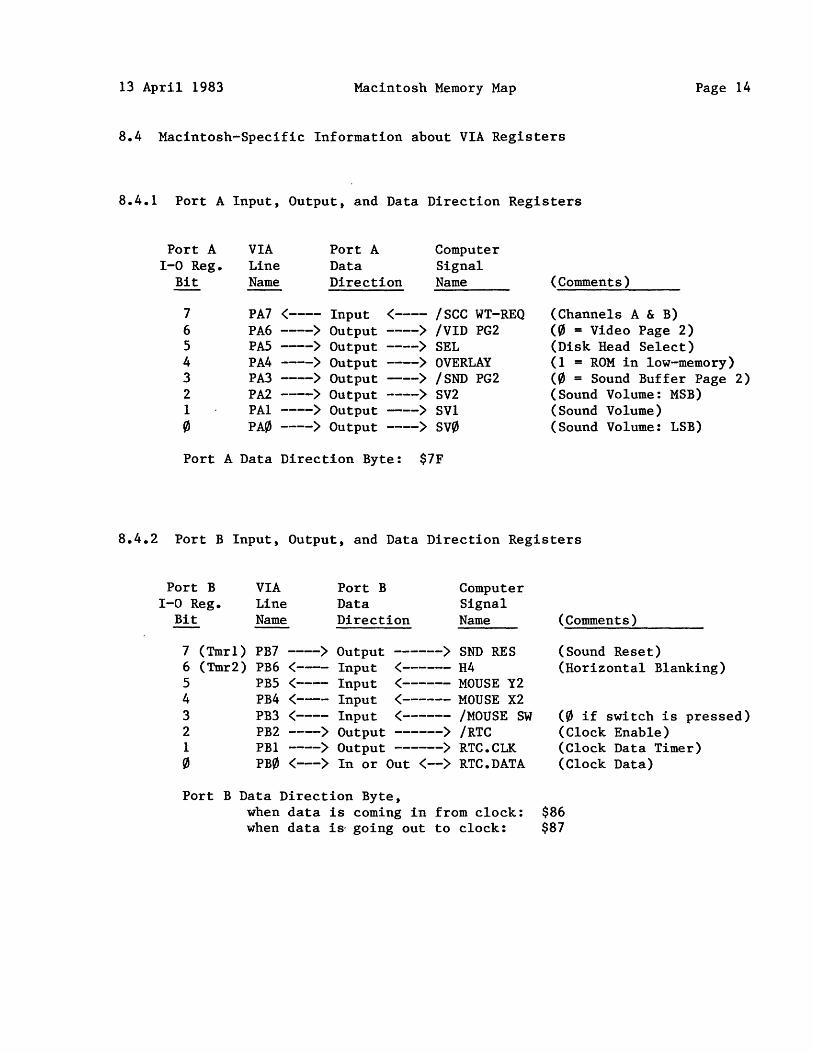
8.4 Macintosh-Specific Information about VIA Registers
8.4.1 Port A Input, Output, and Data Direction Registers
Port A VIA Port A Computer 1-0 Reg. Line Data Signal
Bit Name Direction Name (Comments)
7 PA7 (---- Input (---- /SCC WT-REQ (Channels A & B) 6 PA6 ----) Output ----) /VID PG2 (0 = Video Page 2) S PAS ----) Output ----) SEL (Disk Head Select) 4 PA4 ----) Output ----) OVERLAY (1 = ROM in low-memory) 3 PA3 ----) Output ---) /SND PG2 (0 = Sound Buffer Page 2) 2 PA2 ----) Output ----) SV2 (Sound Volume: MSB) 1 PAl ----) Output ---) SVI (Sound Volume) 0 PA'/J ----) Output ----) sv0 (Sound Volume: LSB)
Port A Data Direction Byte: $7F
8.4.2 Port B Input, Output, and Data Direction Registers
Port B 1-0 Reg.
Bit
VIA Line Name
Port B Data Direction
Computer Signal Name
7 (TmrI) PB7 ----) Output ------) SND RES 6 (Tmr2) PB6 <---- Input <------ H4 S PBS (---- Input <------ MOUSE Y2 4 PB4 (--- Input (------ MOUSE X2 3 PB3 (---- Input (------ /MOUSE SW 2 PB2 ----) Output ------) /RTC 1 PBI ----) Output ------) RTC.CLK o PB'/J <---) In or Out <--) RTC.DATA
Port B Data Direction Byte,
(Comments)
(Sound Reset) (Horizontal Blanking)
('/J if switch is pressed) (Clock Enable) (Clock Data Timer) (Clock Data)
when data is coming in from clock: $86 when data is' going out to clock: $87

13 April 1983 Macintosh Memory Map Page 15
8.4.3 Control Registers
Peripheral VIA Computer Signal Control Line or Interrupt
Register Bit Controlled Controlled (Comments)
7 6 CB2 <-----) KBD.DATA (Keyboard Data) 5 4 CBl <-----) KBD.SCLK (Clock for Keyboard Data) 3 2 CA2 <----- ISEC CLKOUT (1 Sec. Clock Interrupt) 1 0 CAl <----- /VSYNC (Video Vertical Blanking)
8.4.4 Interrupt Flag and Enable Registers
Interrupt VIA Computer Flag Reg. Function Signal
Bit Flagged Flagged (Comments)
7 /IRQ (any Also sets /VIA IRQ (/IPL0) enabled VIA interrupts)
6 Timer 1 (PB7) SND RESET (Sound Timer) 5 Timer 2 4 CBl KBD.SCLK (Clock for Keyboard Data) 3 CB2 KBD.DATA (Keyboard Data) 2 Shift Register Eight bits of KBD.DATA Shifted 1 CAl /VSYNC (Video Vertical Blanking) 0 CA2 ISEC CLKOUT (1 Sec. Clock Interrupt)
The Interrupt Enable Register is arranged just like the Interrupt Flag Register except that bit 7 is "Set/Clear":
Bit 7 Value
1
Meaning of Values In Bits 6 Through 0
Each 1 enables the corresponding interrupt
Each 0 enables the corresponding interrupt

13 April 1983 Macintosh Memory Map Page 16
9. PHASE READ
Note: PHASE READ is one of the functions of the TSG. It allows the programmer to determine (usually at power-up) whether the computer's high-frequency timing signals are correctly in phase, or out of phase and needing correction.
/VPA ----) Decode 1 (A23-21)
A19 ----) Decode 2
8M ----) Sample 1 4M ----) Sample 2
16M ----) Clock
Output ----) D0
PHASE READ Function of the TSG
U3D
9.1 Address Decoding to Activate PHASE READ
Device Address Lines But Do Addressed A23 A22 A21 A2f/J A19 Not Use
PHASE READ 1 1 1 X 0 11100: VIA (/vPA=0, also on bus
A19=0)
(Note: X indicates "don't care": either 1 or 0)
Address Range (Exceptions)
$E00000-$E7FFFF and $F0f/J00f/J-$F7FFFF (But do not use $E0f/J000-$E7FFFF)
13 April 1983 Macintosh Memory Map Page 17
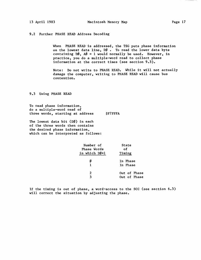
9.2 Further PHASE READ Address Decoding
When PHASE READ-is addressed, the TSG puts phase information on the lowest data line, D0. To read the lower data byte containing D0, A0 = 1 would normally be used. However, in practice, you do a multiple-word read to collect phase information at the correct times (see section 9.3).
Note: Do not write to PHASE READ. While it will not actually damage the computer, writing to PHASE READ will cause bus contention.
9.3 Using PHASE READ
To read phase information, do a multiple-word read of three words, starting at address
The lowest data bit (D0) in each of the three words then contains the desired phase information, which can be interpreted as follows:
Number of Phase Words
in which D0=1
0 1
2 3
$F7FFFA
State of
Timing
In Phase In Phase
Out of Phase Out of Phase
If the timing is out of phase, a word-access to the see (see section 6.3) will correct the situation by adjusting the phase.
13 April 1983 Macintosh Memory Map Page 18
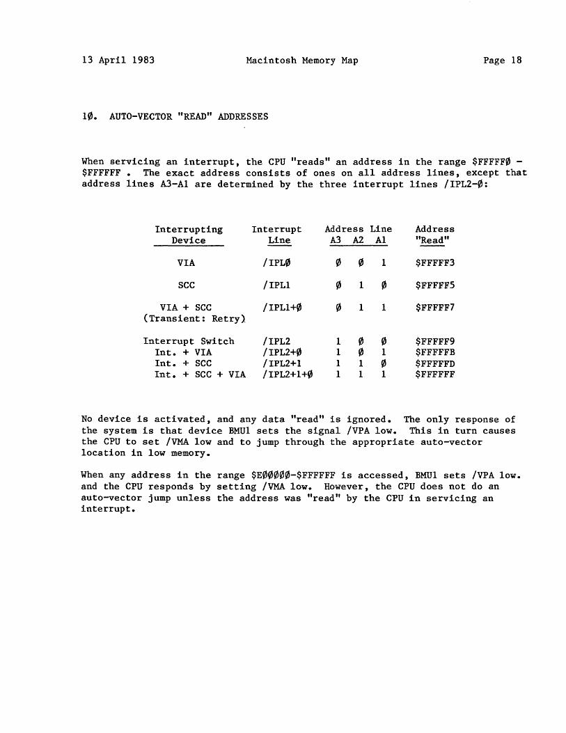
10. AUTO-VECTOR "READ" ADDRESSES
When servicing an interrupt, the CPU "reads" an address in the range $FFFFF0 -$FFFFFF. The exact address consists of ones on all address lines, except that address lines A3-Al are determined by the three interrupt lines /IPL2-0:
Interrupting Interrupt Address Line Address Device Line A3 A2 Al "Read"
VIA /IPL9) 0 9) I $FFFFF3
SCC /IPLI 0 I 0 $FFFFF5
VIA + SCC /IPLl+0 91 1 I $FFFFF7 (Transient: Retry)
Interrupt Switch /IPL2 1 91 91 $FFFFF9 Int. + VIA /IPL2+0 1 0 I $FFFFFB Int. + SCC /IPL2+1 1 1 91 $FFFFFD Int. + SCC + VIA /IPL2+1+91 I 1 1 $FFFFFF
No device is activated, and any data "read" is ignored. The only response of the system is that device BMUI sets the signal /VPA low. This in turn causes the CPU to set /VMA low and to jump through the appropriate auto-vector location in low memory.
When any address in the range $E091000-$FFFFFF is accessed, BMUI sets /VPA low. and the CPU responds by setting /VMA low. However, the CPU does not do an auto-vector jump unless the address was "read" by the CPU in servicing an interrupt.

13 April 1983 Macintosh Memory Map Page 19
11. SOME USEFUL DECODING EQUATIONS
Note: while some device functions are selected by address lines directly, others are selected by Macintosh signals which are internally decoded as follows:
/ROMEN = 9) when OVERLAY=l and A23=0 and A22=0 or when OVERLAY=l and A23=0 and A22=1 and A21=0 or when OVERLAY=0, and A23=0 and A22=1 or when A23=1 and A22=0 or when A23=1 and A22=1 and A21=0
/RAMEN = 0 when OVERLAY=l and A23=0 and A22=1 and A21=1 or when OVERLAY=0 and A23=0 and A22=0 or when A23=1 and A22=0
/RAM READ = 0 when /RAMEN=0 and /ROMEN=1 and R/W=l and /DTACK=0
RAM R/W = 0 when /RAMEN=0 and /ROMEN=1 and R/w=0 and /DTACK=0
/SCC EN = 9) when /As=0 and A23=1 and A22=0
/SCC RD = 0 when /As=0 and A23=1 and A22=0 and A21=0
/IWM = 0
/VPA = 0
/VMA = 9)
/A20 = 9)
when /As=0 and A23=1 and A22=1 and A21=0
when /As=0 and A23=1 and A22=1 and A21=1
when /vPA=0
when A20=1
Phase Info on D0 when /vPA=0 and A19=0