Embed Size (px)
Citation preview
Chu et al., Sci. Adv. 2020; 6 : eaaw7453 14 February 2020
S C I E N C E A D V A N C E S | R E S E A R C H A R T I C L E
1 of 8
M A T E R I A L S S C I E N C E
Low-frequency lattice phonons in halide perovskites explain high defect tolerance toward electron-hole recombinationWeibin Chu1,2, Qijing Zheng1, Oleg V. Prezhdo2, Jin Zhao1,3,4*, Wissam A. Saidi5*
Low-cost solution-based synthesis of metal halide perovskites (MHPs) invariably introduces defects in the system, which could form Shockley-Read-Hall (SRH) electron-hole recombination centers detrimental to solar conversion efficiency. Here, we investigate the nonradiative recombination processes due to native point defects in methyl ammonium lead halide (MAPbI3) perovskites using ab initio nonadiabatic molecular dynamics within surface-hopping framework. Regardless of whether the defects introduce a shallow or deep band state, we find that charge recombination in MAPbI3 is not enhanced, contrary to predictions from SRH theory. We demonstrate that this strong tolerance against defects, and hence the breakdown of SRH, arises because the photogenerated carriers are only coupled with low-frequency phonons and electron and hole states overlap weakly. Both factors appreciably decrease the nonadiabatic coupling. We argue that the soft nature of the inorganic lattice with small bulk modulus is key for defect tolerance, and hence, the findings are general to other MHPs.
INTRODUCTIONThe metal halide perovskites (MHPs) have enormous potential for optoelectronic applications including solar cells and light-emitting diodes. Several studies have shown that methylammonium lead halide perovskites MAPbX3 (MA = CH3NH3; X = Cl, Br, I), and especially MAPbI3, have many unique properties, such as high optical absorptions (1, 2), long electron-hole (e-h) diffusion lengths (3, 4), shallow dominant point defects (5–7), and electronically benign grain boundaries (7, 8). Because of intensive research and interest in these materials, we have witnessed, in the past 10 years, a marked increase in the power conversion efficiencies (PCEs) of MHP-based solar cells from 3.5 to 23.3% (9), which is comparable to record effi-ciencies of commercial thin-film copper indium gallium diselenide and CdTe- based solar cells (10, 11). Nevertheless, the reported PCE is still inferior to the Shockley-Queisser’s theoretical limit of 30 to 33% for solar absorbers with band gaps in the 1.2 to 1.6 eV energy range (12, 13). This calls for a better understanding of efficiency losses due to electron-hole recombinations that are predominantly nonradiative (14–16).
The low-cost synthesis of perovskites is one of the main attrac-tive features of these new photo-absorbers. However, because of the relatively soft ionic nature of MHPs, this approach will invariably introduce different intrinsic or extrinsic dopants in the system (17–20). In traditional semiconductors, cation or anion doping can produce defect states in the band gap, which may form e-h recombination centers via the Shockley-Read-Hall (SRH) process, and consequently
suppress the solar energy conversion efficiency by converting the photon energy into heat (21). While several theoretical studies con-cluded that thermodynamically stable intrinsic defects in MAPbI3 have relatively shallow defect states and hence are electronically benign (1, 6, 7, 22, 23), these conclusions are based on static T = 0 K calculations without accounting for the inelastic electron-phonon interactions. Given that the effective working temperature of a solar cell at room temperature with a PCE of 20% exceeds 343 K (24), temperature effects cannot be ignored. Previous studies have shown that temperature plays a notable effect on solar efficiency such as decreasing the open-circuit voltage Voc of MAPbI3-based solar cells from 1.01 to 0.83 V as the temperature increases from 300 to 360 K (25). In part, Voc drop could be due to the renormalization of the band gap of MAPbI3 with temperature, which is of the order of 30 to 40 meV in the temperature range of solar cell operation (26–29). In addition, the degradation of PCE with temperature could be due to enhancements in the inelastic scattering between defect and charged carriers, as these are mediated by electron-phonon coupling. Although a couple of studies have recently investigated nonradiative processes in MAPbI3 (30, 31), a comprehensive understanding of how defects affect the e-h recombination in the MHPs and how these differ from traditional semiconductors is still lacking.
Here, we study, in detail, the interplay between nonradiative e-h recombination processes and point defects in MAPbI3 using a non-adiabatic molecular dynamics (NAMD) approach. Considering only the intrinsic point defects in MAPbI3, there are three types of vacancy defects (IV, PbV, and MAV), three interstitial defects (Ii, MAi, and Pbi), and six antisite defects (IMA, MAI, PbI, IPb, PbMA, and MAPb, where AB indicates that A is substituted by B). Among these 12 types, we focus our study on defects that have low formation energies and thus are abundant during synthesis. These include I interstitial (Ii), MA substituted by I (MAI) or Pb (MAPb), Pb vacancy (PbV), and I vacancy (IV) (7). While these defects are found to display distinctly different electronic structures by either having mid-gap or shallow p- or n-type defect states, we show that surprisingly these defects do not accelerate e-h recombination. We find that the charge recombination for the Ii
1ICQD/Hefei National Laboratory for Physical Sciences at the Microscale, CAS Key Laboratory of Strongly-Coupled Quantum Matter Physics, and Department of Physics, University of Science and Technology of China, Hefei, Anhui 230026, China. 2Depart-ments of Chemistry, and Physics and Astronomy, University of Southern California, Los Angeles, CA 90089, USA. 3Department of Physics and Astronomy, University of Pittsburgh, Pittsburgh, PA 15260, USA. 4Synergetic Innovation Center of Quantum Information and Quantum Physics, University of Science and Technology of China, Hefei, Anhui 230026, China. 5Department of Mechanical Engineering and Materials Science, University of Pittsburgh, Pittsburgh, PA 15261, USA.*Corresponding author. Email: [email protected] (W.A.S.); [email protected] (J.Z.)
Copyright © 2020 The Authors, some rights reserved; exclusive licensee American Association for the Advancement of Science. No claim to original U.S. Government Works. Distributed under a Creative Commons Attribution NonCommercial License 4.0 (CC BY-NC).
on March 29, 2020
http://advances.sciencemag.org/
Dow
nloaded from
Chu et al., Sci. Adv. 2020; 6 : eaaw7453 14 February 2020
S C I E N C E A D V A N C E S | R E S E A R C H A R T I C L E
2 of 8
system is even suppressed by a factor of 2 compared to the pristine system. We further find that for both the pristine and defective sys-tems, the photogenerated carriers are only coupled with low-frequency phonons, which notably decrease the nonadiabatic coupling (NAC) between the donor and acceptor states. Therefore, both the pristine and defective systems have a long e-h recombination time. We propose that these conclusions are general for all hybrid organic- inorganic perovskite solar cells and may extend to other semi-conductors with low-frequency lattice phonons.
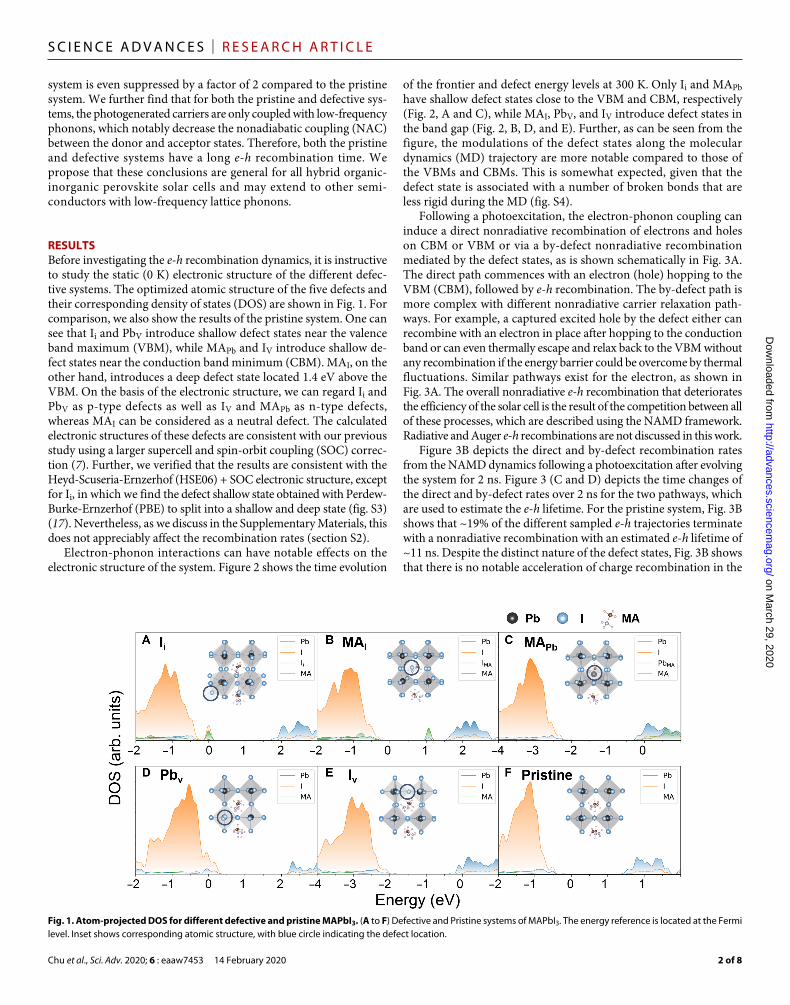
RESULTSBefore investigating the e-h recombination dynamics, it is instructive to study the static (0 K) electronic structure of the different defec-tive systems. The optimized atomic structure of the five defects and their corresponding density of states (DOS) are shown in Fig. 1. For comparison, we also show the results of the pristine system. One can see that Ii and PbV introduce shallow defect states near the valence band maximum (VBM), while MAPb and IV introduce shallow de-fect states near the conduction band minimum (CBM). MAI, on the other hand, introduces a deep defect state located 1.4 eV above the VBM. On the basis of the electronic structure, we can regard Ii and PbV as p-type defects as well as IV and MAPb as n-type defects, whereas MAI can be considered as a neutral defect. The calculated electronic structures of these defects are consistent with our previous study using a larger supercell and spin-orbit coupling (SOC) correc-tion (7). Further, we verified that the results are consistent with the Heyd-Scuseria-Ernzerhof (HSE06) + SOC electronic structure, except for Ii, in which we find the defect shallow state obtained with Perdew- Burke-Ernzerhof (PBE) to split into a shallow and deep state (fig. S3) (17). Nevertheless, as we discuss in the Supplementary Materials, this does not appreciably affect the recombination rates (section S2).
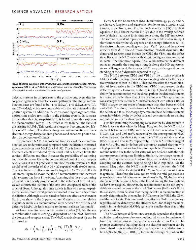
Electron-phonon interactions can have notable effects on the electronic structure of the system. Figure 2 shows the time evolution
of the frontier and defect energy levels at 300 K. Only Ii and MAPb have shallow defect states close to the VBM and CBM, respectively (Fig. 2, A and C), while MAI, PbV, and IV introduce defect states in the band gap (Fig. 2, B, D, and E). Further, as can be seen from the figure, the modulations of the defect states along the molecular dynamics (MD) trajectory are more notable compared to those of the VBMs and CBMs. This is somewhat expected, given that the defect state is associated with a number of broken bonds that are less rigid during the MD (fig. S4).
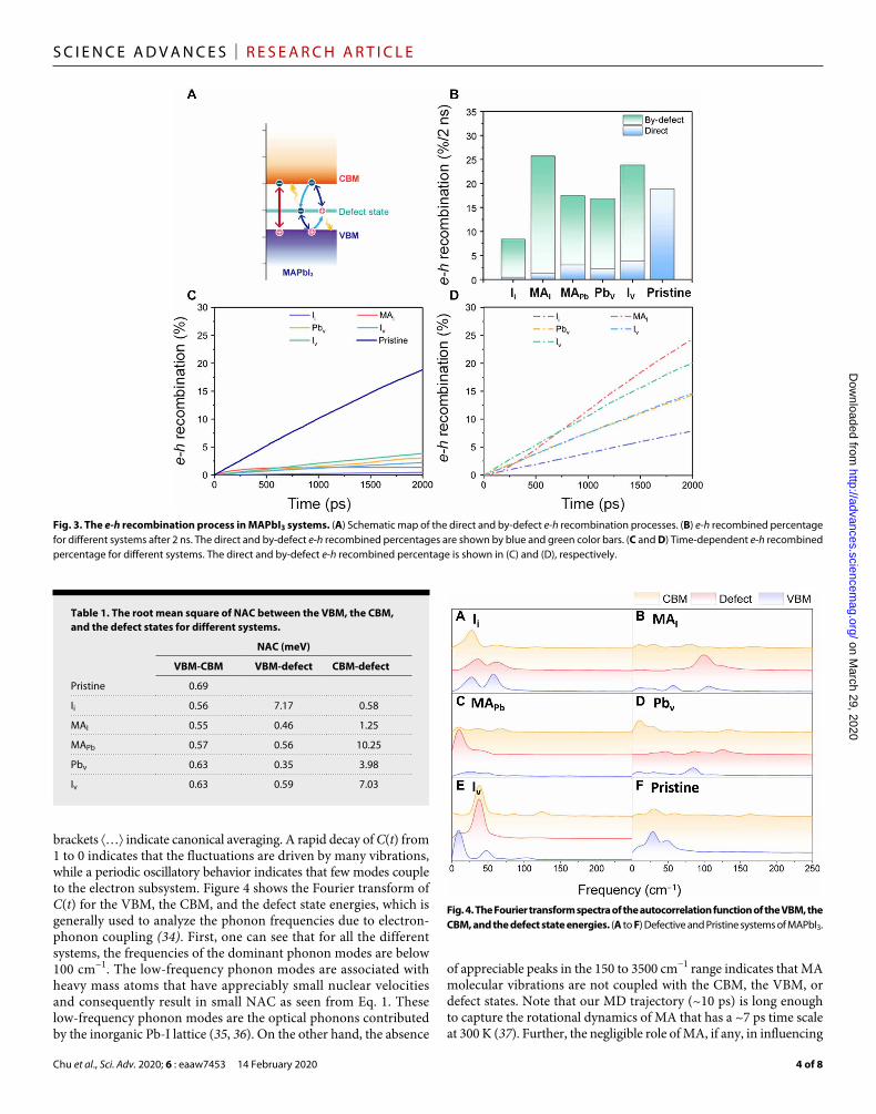
Following a photoexcitation, the electron-phonon coupling can induce a direct nonradiative recombination of electrons and holes on CBM or VBM or via a by-defect nonradiative recombination mediated by the defect states, as is shown schematically in Fig. 3A. The direct path commences with an electron (hole) hopping to the VBM (CBM), followed by e-h recombination. The by-defect path is more complex with different nonradiative carrier relaxation path-ways. For example, a captured excited hole by the defect either can recombine with an electron in place after hopping to the conduction band or can even thermally escape and relax back to the VBM without any recombination if the energy barrier could be overcome by thermal fluctuations. Similar pathways exist for the electron, as shown in Fig. 3A. The overall nonradiative e-h recombination that deteriorates the efficiency of the solar cell is the result of the competition between all of these processes, which are described using the NAMD framework. Radiative and Auger e-h recombinations are not discussed in this work.
Figure 3B depicts the direct and by-defect recombination rates from the NAMD dynamics following a photoexcitation after evolving the system for 2 ns. Figure 3 (C and D) depicts the time changes of the direct and by-defect rates over 2 ns for the two pathways, which are used to estimate the e-h lifetime. For the pristine system, Fig. 3B shows that ~19% of the different sampled e-h trajectories terminate with a nonradiative recombination with an estimated e-h lifetime of ~11 ns. Despite the distinct nature of the defect states, Fig. 3B shows that there is no notable acceleration of charge recombination in the
Fig. 1. Atom-projected DOS for different defective and pristine MAPbI3. (A to F) Defective and Pristine systems of MAPbI3. The energy reference is located at the Fermi level. Inset shows corresponding atomic structure, with blue circle indicating the defect location.
on March 29, 2020
http://advances.sciencemag.org/
Dow
nloaded from
Chu et al., Sci. Adv. 2020; 6 : eaaw7453 14 February 2020
S C I E N C E A D V A N C E S | R E S E A R C H A R T I C L E
3 of 8
defected systems in comparison to the pristine one, even after in-corporating the new by-defect carrier pathways. The charge recom-bination rates are found to be ~17% (MAPb), 17% (MAI), 24% (IV), and 25% (MAI), which are comparable with the rate obtained in the pristine system. In addition, the corresponding charge recombi-nation time scales are similar to the pristine system. In contrast to the other defects, surprisingly, Ii is found to notably suppress the recombination rate to ~9%, which is less than half the value of the pristine MAPbI3. This results in a longer e-h recombination life-time of ~23 ns for Ii. The slower charge recombination time reduces electronic energy dissipation into phonons and enhances photon-to- electron conversion efficiency.
The predicted NAMD nanosecond time scales of the e-h recom-bination are underestimated compared with the lifetime measured experimentally in neat MAPbI3 (3, 4, 32). This is likely due to con-finement effects introduced by the small unit cell, which limits the carriers’ diffusion and thus increases the probability of scattering and recombination. Given the computational cost of first-principles calculations, it is not practical to simulate realistic system size that would be of the order of 20 × 20 × 20 supercell with 40,000 atoms. To assess finite size effects, we used a larger 2 × 2 × 2 supercell with 384 atoms. Figure S1 shows that the e-h recombination time increases with systems size from 11 to 64 ns. Assuming that the e-h scattering probability is linearly proportional to the volume of the unit cell, we can estimate the lifetime of the 20 × 20 × 20 supercell to be of the order of 60 s. Although this time scale is in line with recent experi-mental values, more investigations are needed to accurately determine the lifetime. Although issues related to finite size effects are shown in fig. S1, we show in the Supplementary Materials that the relative magnitude in the e-h recombination rates between the pristine and defective MAPbI3 is less sensitive to the unit cell size (section S1).
As have been discussed in the previous studies (33, 34), the e-h recombination rate is strongly dependent on the NAC between the donor and acceptor states. The NAC matrix element djk can be expressed as
d jk = ⟨ φ j ∣ ∂ ─ ∂ t ∣ φ k ⟩ = ⟨ φ j ∣ ∇ R H∣ φ k ⟩
──────────── ϵ k − ϵ j R ̇ (1)
Here, H is the Kohn-Sham (KS) Hamiltonian; φj, φk, ϵj, and ϵk are the wave functions and eigenvalues for donor and acceptor states j and k, respectively; and Ṙ is the nuclear velocity (34). The first equality in Eq. 1 shows that the NAC is due to the overlap between two orbitals at adjacent ionic time steps along the MD trajectory. The second equivalent representation of the NAC matrix in Eq. 1 shows more clearly that djk depends on the energy difference ϵk − ϵj, the electron-phonon coupling term ⟨φj ∣ ∇RH ∣ φk⟩, and the nuclear velocity term Ṙ. In the e-h recombination NAMD dynamics, the donor and acceptor states include the CBM, the VBM, and the defect state. Because the NAC varies with atomic configurations, we report in Table 1 the root mean square NAC values between the different states to quantify the coupling strength along the MD trajectory. As we will argue next, the average NAC can provide a good under-standing of the e-h dynamics reported in Fig. 3.
The NAC between CBM and VBM of the pristine system is 0.69 meV, which is larger than all corresponding values for the defec-tive systems as shown in Table 1. This indicates that the recombina-tion of free carriers in the CBM and VBM is suppressed in the defective systems. However, as shown in Fig. 3 (B and C), the prob-ability for recombination via the direct path in the defected systems is markedly smaller than that of the pristine one. This apparent in-consistency is because the NAC between defect with either CBM or VBM is larger by one order of magnitude than that between CBM and VBM. Therefore, the electron or hole is likely to be trapped by the defect, and thus, the charge dynamics in these defective systems are mainly driven by the by-defect path and concomitantly restraining recombination via the direct path.
Further, examining the coupling values for the by-defect route in Table 1, we see that while for MAPb, PbV, and IV, the NAC matrix element between the CBM and the defect state is relatively large (10.25, 3.98, and 7.03 meV, respectively), the corresponding NAC values between the defect state and the VBM are notably smaller (0.56, 0.35, and 0.59 meV, respectively). These NAC values suggest that MAPb, PbV, and IV defects will capture an excited electron with a high probability but are less likely to trap a hole. Therefore, the e-h recombination due to the defect states will not be facile, with the hole capture process being rate limiting. Similarly, the charge recombi-nation for Ii systems is also hindered because the defect has a weak coupling for the electron despite being a hole trap state. For the neutral MAI defect, the NAC matrix elements between the VBM (CBM) and the defect state are 0.46 (1.25) meV, which are of similar magnitude. Therefore, the MAI system with the mid-gap state is a potential e-h recombination center. As shown in Fig. 3B, the by-defect charge recombination in MAI is the fastest among the five systems we have investigated. However, the recombination rate is not appre-ciably accelerated because of the small NAC values (0.46 meV). From this analysis, it can be seen that the by-defect e-h recombination is mostly determined by the smallest NAC among the VBM, the CBM, and the defect state. This is referred to as effective NAC. In summary, regardless of the defect type, the effective NAC for charge recombi-nation in the defective MAPbI3 systems is smaller than that of the pristine system.
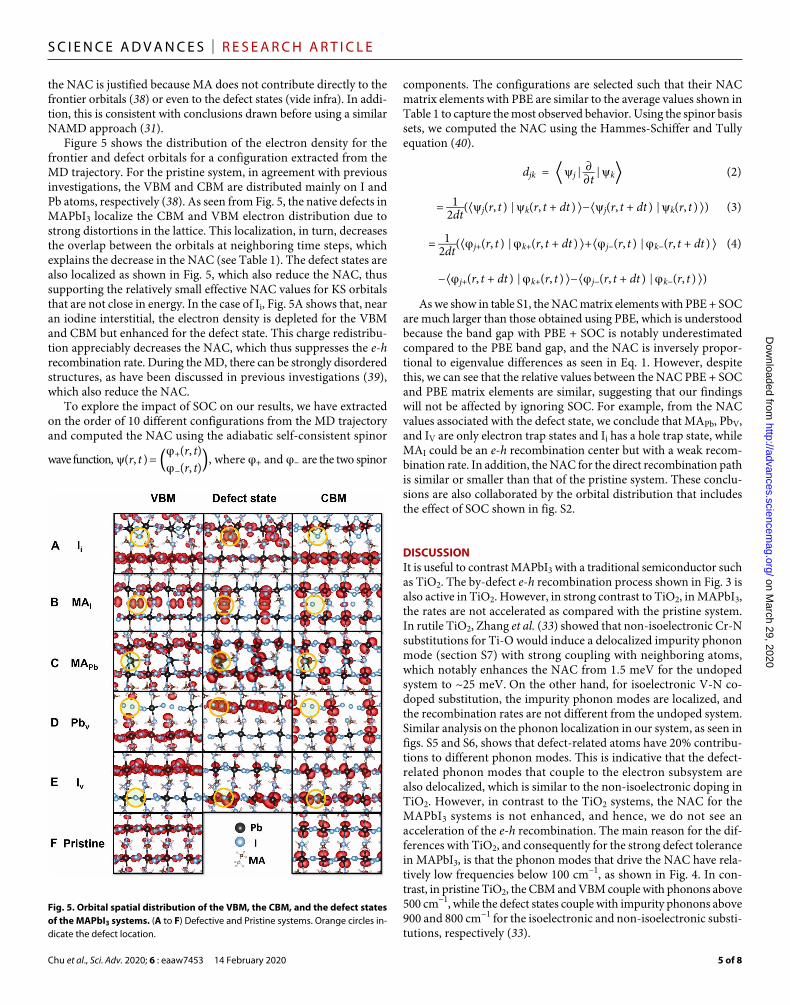
The NACs between different states strongly depend on the phonon excitation and electron-phonon coupling, which can be understood from the fluctuations in the band energies shown in Fig. 2. The phonon excitations that coupled to the electron subsystem can be determined by examining the (normalized) autocorrelation func-tion C(t) = ⟨E(t)E(0)⟩/⟨E(0)E(0)⟩ for the state energy E(t), where the
Fig. 2. The time evolution of the VBM, the CBM, and the defect state for MAPbI3 systems at 300 K. (A to F) Defective and Pristine systems of MAPbI3. The energy reference is located at the VBM of the initial configuration.
on March 29, 2020
http://advances.sciencemag.org/
Dow
nloaded from
Chu et al., Sci. Adv. 2020; 6 : eaaw7453 14 February 2020
S C I E N C E A D V A N C E S | R E S E A R C H A R T I C L E
4 of 8
brackets ⟨…⟩ indicate canonical averaging. A rapid decay of C(t) from 1 to 0 indicates that the fluctuations are driven by many vibrations, while a periodic oscillatory behavior indicates that few modes couple to the electron subsystem. Figure 4 shows the Fourier transform of C(t) for the VBM, the CBM, and the defect state energies, which is generally used to analyze the phonon frequencies due to electron- phonon coupling (34). First, one can see that for all the different systems, the frequencies of the dominant phonon modes are below 100 cm−1. The low-frequency phonon modes are associated with heavy mass atoms that have appreciably small nuclear velocities and consequently result in small NAC as seen from Eq. 1. These low-frequency phonon modes are the optical phonons contributed by the inorganic Pb-I lattice (35, 36). On the other hand, the absence
of appreciable peaks in the 150 to 3500 cm−1 range indicates that MA molecular vibrations are not coupled with the CBM, the VBM, or defect states. Note that our MD trajectory (~10 ps) is long enough to capture the rotational dynamics of MA that has a ~7 ps time scale at 300 K (37). Further, the negligible role of MA, if any, in influencing
Fig. 4. The Fourier transform spectra of the autocorrelation function of the VBM, the CBM, and the defect state energies. (A to F) Defective and Pristine systems of MAPbI3.
Fig. 3. The e-h recombination process in MAPbI3 systems. (A) Schematic map of the direct and by-defect e-h recombination processes. (B) e-h recombined percentage for different systems after 2 ns. The direct and by-defect e-h recombined percentages are shown by blue and green color bars. (C and D) Time-dependent e-h recombined percentage for different systems. The direct and by-defect e-h recombined percentage is shown in (C) and (D), respectively.
Table 1. The root mean square of NAC between the VBM, the CBM, and the defect states for different systems.
NAC (meV)
VBM-CBM VBM-defect CBM-defect
Pristine 0.69
Ii 0.56 7.17 0.58
MAI 0.55 0.46 1.25
MAPb 0.57 0.56 10.25
Pbv 0.63 0.35 3.98
Iv 0.63 0.59 7.03
on March 29, 2020
http://advances.sciencemag.org/
Dow
nloaded from
Chu et al., Sci. Adv. 2020; 6 : eaaw7453 14 February 2020
S C I E N C E A D V A N C E S | R E S E A R C H A R T I C L E
5 of 8
the NAC is justified because MA does not contribute directly to the frontier orbitals (38) or even to the defect states (vide infra). In addi-tion, this is consistent with conclusions drawn before using a similar NAMD approach (31).
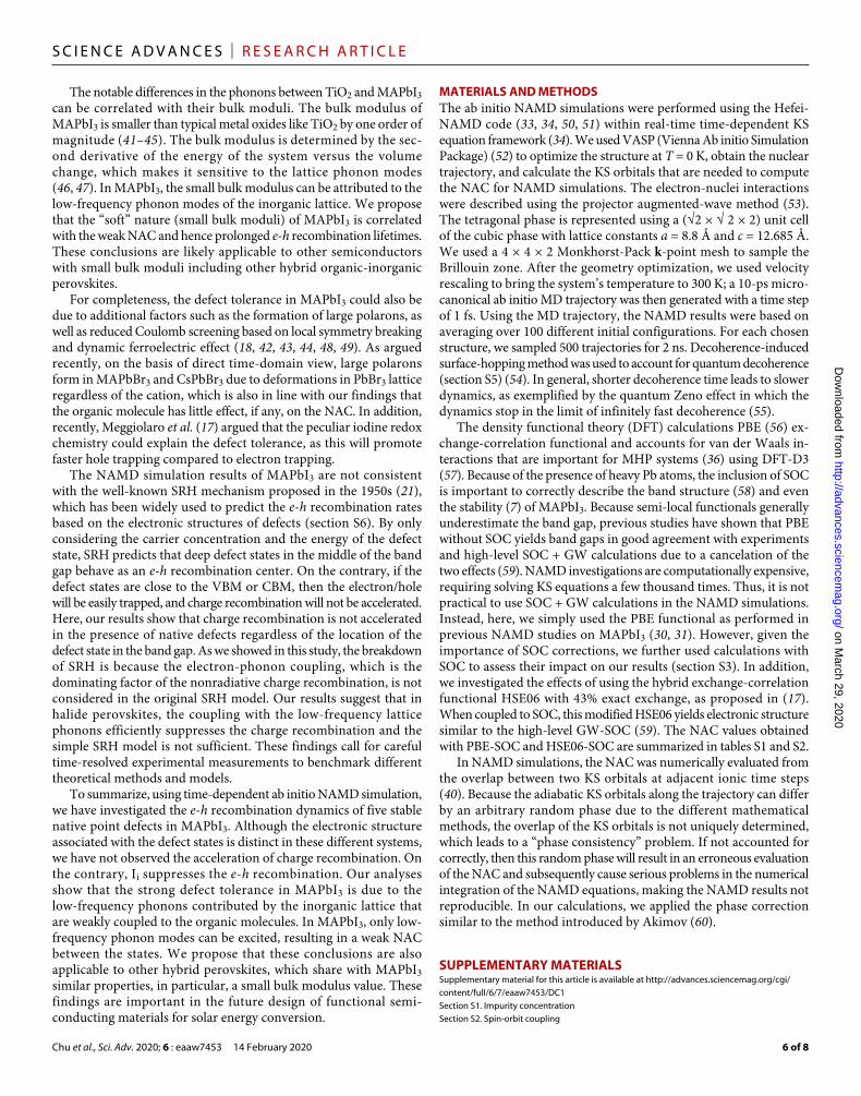
Figure 5 shows the distribution of the electron density for the frontier and defect orbitals for a configuration extracted from the MD trajectory. For the pristine system, in agreement with previous investigations, the VBM and CBM are distributed mainly on I and Pb atoms, respectively (38). As seen from Fig. 5, the native defects in MAPbI3 localize the CBM and VBM electron distribution due to strong distortions in the lattice. This localization, in turn, decreases the overlap between the orbitals at neighboring time steps, which explains the decrease in the NAC (see Table 1). The defect states are also localized as shown in Fig. 5, which also reduce the NAC, thus supporting the relatively small effective NAC values for KS orbitals that are not close in energy. In the case of Ii, Fig. 5A shows that, near an iodine interstitial, the electron density is depleted for the VBM and CBM but enhanced for the defect state. This charge redistribu-tion appreciably decreases the NAC, which thus suppresses the e-h recombination rate. During the MD, there can be strongly disordered structures, as have been discussed in previous investigations (39), which also reduce the NAC.
To explore the impact of SOC on our results, we have extracted on the order of 10 different configurations from the MD trajectory and computed the NAC using the adiabatic self-consistent spinor
wave function, (r, t ) = ( φ + (r, t)
φ − (r, t)
) , where φ+ and φ− are the two spinor
components. The configurations are selected such that their NAC matrix elements with PBE are similar to the average values shown in Table 1 to capture the most observed behavior. Using the spinor basis sets, we computed the NAC using the Hammes-Schiffer and Tully equation (40).
d jk = ⟨ j ∣ ∂ ─ ∂ t ∣ k ⟩ (2)
= 1 ─ 2dt (⟨ j (r, t ) ∣ k (r, t + dt ) ⟩− ⟨ j (r, t + dt ) ∣ k (r, t ) ⟩) (3)
= 1 ─ 2dt (⟨ φ j+ (r, t ) ∣ φ k+ (r, t + dt ) ⟩+ ⟨ φ j− (r, t ) ∣ φ k− (r, t + dt ) ⟩ (4)
− ⟨ φ j+ (r, t + dt ) ∣ φ k+ (r, t ) ⟩− ⟨ φ j− (r, t + dt ) ∣ φ k− (r, t ) ⟩)
As we show in table S1, the NAC matrix elements with PBE + SOC are much larger than those obtained using PBE, which is understood because the band gap with PBE + SOC is notably underestimated compared to the PBE band gap, and the NAC is inversely propor-tional to eigenvalue differences as seen in Eq. 1. However, despite this, we can see that the relative values between the NAC PBE + SOC and PBE matrix elements are similar, suggesting that our findings will not be affected by ignoring SOC. For example, from the NAC values associated with the defect state, we conclude that MAPb, PbV, and IV are only electron trap states and Ii has a hole trap state, while MAI could be an e-h recombination center but with a weak recom-bination rate. In addition, the NAC for the direct recombination path is similar or smaller than that of the pristine system. These conclu-sions are also collaborated by the orbital distribution that includes the effect of SOC shown in fig. S2.
DISCUSSIONIt is useful to contrast MAPbI3 with a traditional semiconductor such as TiO2. The by-defect e-h recombination process shown in Fig. 3 is also active in TiO2. However, in strong contrast to TiO2, in MAPbI3, the rates are not accelerated as compared with the pristine system. In rutile TiO2, Zhang et al. (33) showed that non-isoelectronic Cr-N substitutions for Ti-O would induce a delocalized impurity phonon mode (section S7) with strong coupling with neighboring atoms, which notably enhances the NAC from 1.5 meV for the undoped system to ~25 meV. On the other hand, for isoelectronic V-N co-doped substitution, the impurity phonon modes are localized, and the recombination rates are not different from the undoped system. Similar analysis on the phonon localization in our system, as seen in figs. S5 and S6, shows that defect-related atoms have 20% contribu-tions to different phonon modes. This is indicative that the defect- related phonon modes that couple to the electron subsystem are also delocalized, which is similar to the non-isoelectronic doping in TiO2. However, in contrast to the TiO2 systems, the NAC for the MAPbI3 systems is not enhanced, and hence, we do not see an acceleration of the e-h recombination. The main reason for the dif-ferences with TiO2, and consequently for the strong defect tolerance in MAPbI3, is that the phonon modes that drive the NAC have rela-tively low frequencies below 100 cm−1, as shown in Fig. 4. In con-trast, in pristine TiO2, the CBM and VBM couple with phonons above 500 cm−1, while the defect states couple with impurity phonons above 900 and 800 cm−1 for the isoelectronic and non-isoelectronic substi-tutions, respectively (33).
Fig. 5. Orbital spatial distribution of the VBM, the CBM, and the defect states of the MAPbI3 systems. (A to F) Defective and Pristine systems. Orange circles in-dicate the defect location.
on March 29, 2020
http://advances.sciencemag.org/
Dow
nloaded from
Chu et al., Sci. Adv. 2020; 6 : eaaw7453 14 February 2020
S C I E N C E A D V A N C E S | R E S E A R C H A R T I C L E
6 of 8
The notable differences in the phonons between TiO2 and MAPbI3 can be correlated with their bulk moduli. The bulk modulus of MAPbI3 is smaller than typical metal oxides like TiO2 by one order of magnitude (41–45). The bulk modulus is determined by the sec-ond derivative of the energy of the system versus the volume change, which makes it sensitive to the lattice phonon modes (46, 47). In MAPbI3, the small bulk modulus can be attributed to the low-frequency phonon modes of the inorganic lattice. We propose that the “soft” nature (small bulk moduli) of MAPbI3 is correlated with the weak NAC and hence prolonged e-h recombination lifetimes. These conclusions are likely applicable to other semiconductors with small bulk moduli including other hybrid organic-inorganic perovskites.
For completeness, the defect tolerance in MAPbI3 could also be due to additional factors such as the formation of large polarons, as well as reduced Coulomb screening based on local symmetry breaking and dynamic ferroelectric effect (18, 42, 43, 44, 48, 49). As argued recently, on the basis of direct time-domain view, large polarons form in MAPbBr3 and CsPbBr3 due to deformations in PbBr3 lattice regardless of the cation, which is also in line with our findings that the organic molecule has little effect, if any, on the NAC. In addition, recently, Meggiolaro et al. (17) argued that the peculiar iodine redox chemistry could explain the defect tolerance, as this will promote faster hole trapping compared to electron trapping.
The NAMD simulation results of MAPbI3 are not consistent with the well-known SRH mechanism proposed in the 1950s (21), which has been widely used to predict the e-h recombination rates based on the electronic structures of defects (section S6). By only considering the carrier concentration and the energy of the defect state, SRH predicts that deep defect states in the middle of the band gap behave as an e-h recombination center. On the contrary, if the defect states are close to the VBM or CBM, then the electron/hole will be easily trapped, and charge recombination will not be accelerated. Here, our results show that charge recombination is not accelerated in the presence of native defects regardless of the location of the defect state in the band gap. As we showed in this study, the breakdown of SRH is because the electron-phonon coupling, which is the dominating factor of the nonradiative charge recombination, is not considered in the original SRH model. Our results suggest that in halide perovskites, the coupling with the low-frequency lattice phonons efficiently suppresses the charge recombination and the simple SRH model is not sufficient. These findings call for careful time-resolved experimental measurements to benchmark different theoretical methods and models.
To summarize, using time-dependent ab initio NAMD simulation, we have investigated the e-h recombination dynamics of five stable native point defects in MAPbI3. Although the electronic structure associated with the defect states is distinct in these different systems, we have not observed the acceleration of charge recombination. On the contrary, Ii suppresses the e-h recombination. Our analyses show that the strong defect tolerance in MAPbI3 is due to the low-frequency phonons contributed by the inorganic lattice that are weakly coupled to the organic molecules. In MAPbI3, only low- frequency phonon modes can be excited, resulting in a weak NAC between the states. We propose that these conclusions are also applicable to other hybrid perovskites, which share with MAPbI3 similar properties, in particular, a small bulk modulus value. These findings are important in the future design of functional semi-conducting materials for solar energy conversion.
MATERIALS AND METHODSThe ab initio NAMD simulations were performed using the Hefei- NAMD code (33, 34, 50, 51) within real-time time-dependent KS equation framework (34). We used VASP (Vienna Ab initio Simulation Package) (52) to optimize the structure at T = 0 K, obtain the nuclear trajectory, and calculate the KS orbitals that are needed to compute the NAC for NAMD simulations. The electron-nuclei interactions were described using the projector augmented-wave method (53). The tetragonal phase is represented using a (√2 × √ 2 × 2) unit cell of the cubic phase with lattice constants a = 8.8 Å and c = 12.685 Å. We used a 4 × 4 × 2 Monkhorst-Pack k-point mesh to sample the Brillouin zone. After the geometry optimization, we used velocity rescaling to bring the system’s temperature to 300 K; a 10-ps micro-canonical ab initio MD trajectory was then generated with a time step of 1 fs. Using the MD trajectory, the NAMD results were based on averaging over 100 different initial configurations. For each chosen structure, we sampled 500 trajectories for 2 ns. Decoherence-induced surface-hopping method was used to account for quantum decoherence (section S5) (54). In general, shorter decoherence time leads to slower dynamics, as exemplified by the quantum Zeno effect in which the dynamics stop in the limit of infinitely fast decoherence (55).
The density functional theory (DFT) calculations PBE (56) ex-change-correlation functional and accounts for van der Waals in-teractions that are important for MHP systems (36) using DFT-D3 (57). Because of the presence of heavy Pb atoms, the inclusion of SOC is important to correctly describe the band structure (58) and even the stability (7) of MAPbI3. Because semi-local functionals generally underestimate the band gap, previous studies have shown that PBE without SOC yields band gaps in good agreement with experiments and high-level SOC + GW calculations due to a cancelation of the two effects (59). NAMD investigations are computationally expensive, requiring solving KS equations a few thousand times. Thus, it is not practical to use SOC + GW calculations in the NAMD simulations. Instead, here, we simply used the PBE functional as performed in previous NAMD studies on MAPbI3 (30, 31). However, given the importance of SOC corrections, we further used calculations with SOC to assess their impact on our results (section S3). In addition, we investigated the effects of using the hybrid exchange-correlation functional HSE06 with 43% exact exchange, as proposed in (17). When coupled to SOC, this modified HSE06 yields electronic structure similar to the high-level GW-SOC (59). The NAC values obtained with PBE-SOC and HSE06-SOC are summarized in tables S1 and S2.
In NAMD simulations, the NAC was numerically evaluated from the overlap between two KS orbitals at adjacent ionic time steps (40). Because the adiabatic KS orbitals along the trajectory can differ by an arbitrary random phase due to the different mathematical methods, the overlap of the KS orbitals is not uniquely determined, which leads to a “phase consistency” problem. If not accounted for correctly, then this random phase will result in an erroneous evaluation of the NAC and subsequently cause serious problems in the numerical integration of the NAMD equations, making the NAMD results not reproducible. In our calculations, we applied the phase correction similar to the method introduced by Akimov (60).
SUPPLEMENTARY MATERIALSSupplementary material for this article is available at http://advances.sciencemag.org/cgi/content/full/6/7/eaaw7453/DC1Section S1. Impurity concentrationSection S2. Spin-orbit coupling
on March 29, 2020
http://advances.sciencemag.org/
Dow
nloaded from
Chu et al., Sci. Adv. 2020; 6 : eaaw7453 14 February 2020
S C I E N C E A D V A N C E S | R E S E A R C H A R T I C L E
7 of 8
Section S3. The validity of using PBE functionalSection S4. Electronic structure change induced by electron-phonon interactionsSection S5. Decoherence effectsSection S6. SRH modelSection S7. The impurity phonon localizationSection S8. Phonon effects on the NAMD of electronic statesFig. S1. The time-dependent e-h recombined percentage for different systems.Fig. S2. The orbital distribution with SOC of the VBM, the CBM, and the defect states for pristine and different defective MAPbI3 systems.Fig. S3. Electronic state levels of CBM spinors (blue line), VBM spinors (purple line), and defect spinors (orange line) of the different MAPbI3 systems for a single configuration at 300 K.Fig. S4. Electron-phonon interactions induce electronic structure changes for Pbv defective MAPbI3 at 300 K.Fig. S5. The total DOS of phonons (blue) and projected DOS of impurity phonons (orange) of the pristine and different defective MAPbI3 systems.Fig. S6. The ratio of impurity phonon modes to the total phonon modes of the pristine and different defective MAPbI3 systems.Table S1. The NAC between the spinor of the VBM, the CBM, and the defect states for different systems when including the effect of SOC.Table S2. The NAC between the spinor states of the VBM, the CBM, and the defect states for different systems calculated at the PBE and HSE06 + SOC.Table S3. The pure dephasing time between the VBM, the CBM, and the defect states for different systems.References (61–69)
REFERENCES AND NOTES 1. W. J. Yin, T. T. Shi, Y. F. Yan, Unique properties of halide perovskites as possible origins
of the superior solar cell performance. Adv. Mater. 26, 4653–4658 (2014). 2. G. Grancini, S. Marras, M. Prato, C. Giannini, C. Quarti, F. De Angelis, M. De Bastiani,
G. E. Eperon, H. J. Snaith, L. Manna, A. Petrozza, The impact of the crystallization processes on the structural and optical properties of hybrid perovskite films for photovoltaics. J. Phys. Chem. Lett. 5, 3836–3842 (2014).
3. G. C. Xing, N. Mathews, S. Y. Sun, S. S. Lim, Y. M. Lam, M. Grätzel, S. Mhaisalkar, T. C. Sum, Long-range balanced electron- and hole-transport lengths in organic-inorganic CH3NH3PbI3. Science 342, 344–347 (2013).
4. S. D. Stranks, G. E. Eperon, G. Grancini, C. Menelaou, M. J. P. Alcocer, T. Leijtens, L. M. Herz, A. Petrozza, H. J. Snaith, Electron-hole diffusion lengths exceeding 1 micrometer in an organometal trihalide perovskite absorber. Science 342, 341–344 (2013).
5. W.-J. Yin, T. T. Shi, Y. F. Yan, Unusual defect physics in CH3NH3PbI3 perovskite solar cell absorber. Appl. Phys. Lett. 104, 063903 (2014).
6. J. Kim, S.-H. Lee, J. H. Lee, K.-H. Hong, The role of intrinsic defects in methylammonium lead iodide perovskite. J. Phys. Chem. Lett. 5, 1312–1317 (2014).
7. W. T. Shan, W. A. Saidi, Segregation of native defects to the grain boundaries in methylammonium lead iodide perovskite. J. Phys. Chem. Lett. 8, 5935–5942 (2017).
8. Y. G. Guo, Q. Wang, W. A. Saidi, Structural stabilities and electronic properties of high-angle grain boundaries in perovskite cesium lead halides. J. Phys. Chem. C 121, 1715–1722 (2017).
9. S. I. Seok, M. Grätzel, N.-G. Park, Methodologies toward highly efficient perovskite solar cells. Small 14, 1704177 (2018).
10. Y. X. Zhao, K. Zhu, Organic–inorganic hybrid lead halide perovskites for optoelectronic and electronic applications. Chem. Soc. Rev. 45, 655–689 (2016).
11. M. A. Green, K. Emery, Y. Hishikawa, W. Warta, E. D. Dunlop, Solar cell efficiency tables (version 45). Prog. Photovolt. 23, 1–9 (2015).
12. W. Shockley, H. J. Queisser, Detailed balance limit of efficiency of p-n junction solar cells. J. Appl. Phys. 32, 510–519 (1961).
13. W. E. I. Sha, X. G. Ren, L. Z. Chen, W. C. H. Choy, The efficiency limit of CH3NH3PbI3 perovskite solar cells. Appl. Phys. Lett. 106, 221104 (2015).
14. K. Tvingstedt, O. Malinkiewicz, A. Baumann, C. Deibel, H. J. Snaith, V. Dyakonov, H. J. Bolink, Radiative efficiency of lead iodide based perovskite solar cells. Sci. Rep. 4, 6071 (2014).
15. J. M. Ball, A. Petrozza, Defects in perovskite-halides and their effects in solar cells. Nat. Energy 1, 16149 (2016).
16. W. Tress, N. Marinova, O. Inganas, M. K. Nazeeruddin, S. M. Zakeeruddin, M. Graetzel, Predicting the open-circuit voltage of CH3NH3PbI3 perovskite solar cells using electroluminescence and photovoltaic quantum efficiency spectra: The role of radiative and non-radiative recombination. Adv. Energy Mater. 5, 1400812 (2015).
17. D. Meggiolaro, S. G. Motti, E. Mosconi, A. J. Barker, J. Ball, C. A. R. Perini, F. Deschler, A. Petrozza, F. De Angelis, Iodine chemistry determines the defect tolerance of lead-halide perovskites. Energy Environ. Sci. 11, 702–713 (2018).
18. Y. Chen, H. T. Yi, X. Wu, R. Haroldson, Y. N. Gartstein, Y. I. Rodionov, K. S. Tikhonov, A. Zakhidov, X. Y. Zhu, V. Podzorov, Extended carrier lifetimes and diffusion in hybrid
perovskites revealed by Hall effect and photoconductivity measurements. Nat. Commun. 7, 12253 (2016).
19. T. Leijtens, G. E. Eperon, A. J. Barker, G. Grancini, W. Zhang, J. M. Ball, A. R. S. Kandada, H. J. Snaith, A. Petrozza, Carrier trapping and recombination: The role of defect physics in enhancing the open circuit voltage of metal halide perovskite solar cells. Energy Environ. Sci. 9, 3472–3481 (2016).
20. D. W. deQuilettes, S. M. Vorpahl, S. D. Stranks, H. Nagaoka, G. E. Eperon, M. E. Ziffer, H. J. Snaith, D. S. Ginger, Impact of microstructure on local carrier lifetime in perovskite solar cells. Science 348, 683–686 (2015).
21. W. Shockley, W. T. Read Jr., Statistics of the recombinations of holes and electrons. Phys. Rev. 87, 835–842 (1952).
22. J. Kang, L. W. Wang, High defect tolerance in lead halide perovskite CsPbBr3. J. Phys. Chem. Lett. 8, 489–493 (2017).
23. H. Huang, M. I. Bodnarchuk, S. V. Kershaw, M. V. Kovalenko, A. L. Rogach, Lead halide perovskite nanocrystals in the research spotlight: Stability and defect tolerance. ACS Energy Lett. 2, 2071–2083 (2017).
24. E. Skoplaki, A. G. Boudouvis, J. A. Palyvos, A simple correlation for the operating temperature of photovoltaic modules of arbitrary mounting. Sol. Energy Mater. Sol. Cells 92, 1393–1402 (2008).
25. H. Zhang, X. Qiao, Y. Shen, T. Moehl, S. M. Zakeeruddin, M. Grätzel, M. Wang, Photovoltaic behaviour of lead methylammonium triiodide perovskite solar cells down to 80 K. J. Mater. Chem. A 3, 11762–11767 (2015).
26. B. J. Foley, D. L. Marlowe, K. Y. Sun, W. A. Saidi, L. Scudiero, M. C. Gupta, J. J. Choi, Temperature dependent energy levels of methylammonium lead iodide perovskite. Appl. Phys. Lett. 106, 243904 (2015).
27. R. L. Milot, G. E. Eperon, H. J. Snaith, M. B. Johnston, L. M. Herz, Temperature-dependent charge-carrier dynamics in CH3NH3PbI3 perovskite thin films. Adv. Funct. Mater. 25, 6218–6227 (2015).
28. W. A. Saidi, S. Ponce, B. Monserrat, Temperature dependence of the energy levels of methylammonium lead iodide perovskite from first-principles. J. Phys. Chem. Lett. 7, 5247–5252 (2016).
29. W. A. Saidi, A. Kachmar, Effects of electron–phonon coupling on electronic properties of methylammonium lead iodide perovskites. J. Phys. Chem. Lett. 9, 7090–7097 (2018).
30. R. Long, J. Liu, O. V. Prezhdo, Unravelling the effects of grain boundary and chemical doping on electron–hole recombination in CH3NH3PbI3 perovskite by time-domain atomistic simulation. J. Am. Chem. Soc. 138, 3884–3890 (2016).
31. W. Li, J. Liu, F.-Q. Bai, H.-X. Zhang, O.-V. Prezhdo, Hole trapping by iodine interstitial defects decreases free carrier losses in perovskite solar cells: A time-domain ab initio study. ACS Energy Lett. 2, 1270–1278 (2017).
32. Y. Yamada, T. Nakamura, M. Endo, A. Wakamiya, Y. Kanemitsu, Photocarrier recombination dynamics in perovskite CH3NH3PbI3 for solar cell applications. J. Am. Chem. Soc. 136, 11610–11613 (2014).
33. L. L. Zhang, Q. J. Zheng, Y. Xie, Z. G. Lan, O. V. Prezhdo, W. A. Saidi, J. Zhao, Delocalized impurity phonon induced electron–hole recombination in doped semiconductors. Nano Lett. 18, 1592–1599 (2018).
34. Q. Zheng, W. Chu, C. Zhao, L. Zhang, H. Guo, Y. Wang, X. Jiang, J. Zhao, Ab initio nonadiabatic molecular dynamics investigations on the excited carriers in condensed matter systems. Wiley Interdiscip. Rev. 9, e1411 (2019).
35. C. Quarti, G. Grancini, E. Mosconi, P. Bruno, J. M. Ball, M. M. Lee, H. J. Snaith, A. Petrozza, F. De Angelis, The Raman spectrum of the CH3NH3Pbl3 hybrid perovskite: Interplay of theory and experiment. J. Phys. Chem. Lett. 5, 279–284 (2014).
36. W. A. Saidi, J. J. Choi, Nature of the cubic to tetragonal phase transition in methylammonium lead iodide perovskite. J. Chem. Phys. 145, 144702 (2016).
37. S. Govinda, B. P. Kore, M. Bokdam, P. Mahale, A. Kumar, S. Pal, B. Bhattacharyya, J. Lahnsteiner, G. Kresse, C. Franchini, A. Pandey, D. D. Sarma, Behavior of methylammonium dipoles in MAPbX3 (X = Br and I). J. Phys. Chem. Lett. 8, 4113–4121 (2017).
38. F. Brivio, A. B. Walker, A. Walsh, Structural and electronic properties of hybrid perovskites for high-efficiency thin-film photovoltaics from first-principles. APL Mater. 1, 042111 (2013).
39. M. L. Agiorgousis, Y. Y. Sun, H. Zeng, S. B. Zhang, Strong covalency-induced recombination centers in perovskite solar cell material CH3NH3Pbl3. J. Am. Chem. Soc. 136, 14570–14575 (2014).
40. S. Hammes-Schiffer, J. C. Tully, Proton transfer in solution: Molecular dynamics with quantum transitions. J. Chem. Phys. 101, 4657–4667 (1994).
41. J. F. Yang, X. M. Wen, H. Z. Xia, R. Sheng, Q. S. Ma, J. Kim, P. Tapping, T. Harada, T. W. Kee, F. Z. Huang, Y. B. Cheng, M. Green, A. Ho-Baillie, S. J. Huang, S. Shrestha, R. Patterson, G. Conibeer, Acoustic-optical phonon up-conversion and hot-phonon bottleneck in lead-halide perovskites. Nat. Commun. 8, 14120 (2017).
42. O. Yaffe, Y. S. Guo, L. Z. Tan, D. A. Egger, T. Hull, C. C. Stoumpos, F. Zheng, T. F. Heinz, L. Kronik, M. G. Kanatzidis, J. S. Owen, A. M. Rappe, M. A. Pimenta, L. E. Brus, Local polar fluctuations in lead halide perovskite crystals. Phys. Rev. Lett. 118, 136001 (2017).
on March 29, 2020
http://advances.sciencemag.org/
Dow
nloaded from
Chu et al., Sci. Adv. 2020; 6 : eaaw7453 14 February 2020
S C I E N C E A D V A N C E S | R E S E A R C H A R T I C L E
8 of 8
43. E. Cinquanta, D. Meggiolaro, S. G. Motti, M. Gandini, M. J. P. Alcocer, Q. A. Akkerman, C. Vozzi, L. Manna, F. De Angelis, A. Petrozza, S. Stagira, Ultrafast THz probe of photoinduced polarons in lead-halide perovskites. Phys. Rev. Lett. 122, 166601 (2019).
44. K. Miyata, D. Meggiolaro, M. T. Trinh, P. P. Joshi, E. Mosconi, S. C. Jones, F. De Angelis, X. Y. Zhu, Large polarons in lead halide perovskites. Sci. Adv. 3, e1701217 (2017).
45. D. L. Anderson, O. L. Anderson, The bulk modulus-volume relationship for oxides. J. Geophys. Res. 75, 3494–3500 (1970).
46. V. G. Baonza, General behavior of longitudinal optical phonons in cubic diatomic crystals. Solid State Commun. 130, 383–386 (2004).
47. F. Aguado, V. G. Baonza, Prediction of bulk modulus at high temperatures from longitudinal phonon frequencies: Application to diamond, c-BN, and 3C-SiC. Phys. Rev. B 73, 024111 (2006).
48. X.-Y. Zhu, V. Podzorov, Charge carriers in hybrid organic-inorganic lead halide perovskites might be protected as large polarons. J. Phys. Chem. Lett. 6, 4758–4761 (2015).
49. K. Miyata, X.-Y. Zhu, Ferroelectric large polarons. Nat. Mater. 17, 379–381 (2018). 50. W. B. Chu, W. A. Saidi, Q. J. Zheng, Y. Xie, Z. G. Lan, O. V. Prezhdo, H. Petek, J. Zhao,
Ultrafast dynamics of photongenerated holes at a CH3OH/TiO2 Rutile Interface. J. Am. Chem. Soc. 138, 13740–13749 (2016).
51. Q. J. Zheng, W. A. Saidi, Y. Xie, Z. G. Lan, O. V. Prezhdo, H. Petek, J. Zhao, Phonon-assisted ultrafast charge transfer at van der Waals heterostructure interface. Nano Lett. 17, 6435–6442 (2017).
52. G. Kresse, J. Hafner, Ab initio molecular dynamics for liquid metals. Phys. Rev. B 47, 558–561 (1993).
53. G. Kresse, D. Joubert, From ultrasoft pseudopotentials to the projector augmented-wave method. Phys. Rev. B 59, 1758–1775 (1999).
54. H. M. Jaeger, S. Fischer, O. V. Prezhdo, Decoherence-induced surface hopping. J. Chem. Phys. 137, 22A545 (2012).
55. S. V. Kilina, A. J. Neukirch, B. F. Habenicht, D. S. Kilin, O. V. Prezhdo, Quantum zeno effect rationalizes the phonon bottleneck in semiconductor quantum dots. Phys. Rev. Lett. 110, 180404 (2013).
56. J. P. Perdew, K. Burke, M. Ernzerhof, Generalized gradient approximation made simple. Phys. Rev. Lett. 77, 3865–3868 (1996).
57. S. Grimme, J. Antony, S. Ehrlich, H. Krieg, A consistent and accurate ab initio parametrization of density functional dispersion correction (DFT-D) for the 94 elements H-Pu. J. Chem. Phys. 132, 154104 (2010).
58. M. H. Du, Efficient carrier transport in halide perovskites: Theoretical perspectives. J. Mater. Chem. A 2, 9091–9098 (2014).
59. P. Umari, E. Mosconi, F. De Angelis, Relativistic GW calculations on CH3NH3PbI3 and CH3NH3SnI3 perovskites for solar cell applications. Sci. Rep. 4, 4467 (2014).
60. A. V. Akimov, A simple phase correction makes a big difference in nonadiabatic molecular dynamics. J. Phys. Chem. Lett. 9, 6096–6102 (2018).
61. Q. F. Dong, Y. J. Fang, Y. C. Shao, P. Mulligan, J. Qiu, L. Cao, J. S. Huang, Electron-hole diffusion lengths > 175 m in solution-grown CH3NH3PbI3 single crystals. Science 347, 967–970 (2015).
62. Y. Yang, M. J. Yang, Z. Li, R. Crisp, K. Zhu, M. C. Beard, Comparison of recombination dynamics in CH3NH3PbBr3 and CH3NH3PbI3 perovskite films: Influence of exciton binding energy. J. Phys. Chem. Lett. 6, 4688–4692 (2015).
63. A. Alkauskas, A. Pasquarello, Band-edge problem in the theoretical determination of defect energy levels: The O vacancy in ZnO as a benchmark case. Phys. Rev. B 84, 125206 (2011).
64. W. M. Chen, B. Monemar, E. Janzén, J. L. Lindström, DIRECT observation of intercenter charge-transfer in dominant nonradiative recombination channels in silicon. Phys. Rev. Lett. 67, 1914–1917 (1991).
65. D. Macdonald, A. Cuevas, Validity of simplified Shockley-Read-Hall statistics for modeling carrier lifetimes in crystalline silicon. Phys. Rev. B 67, 075203 (2003).
66. S. Rein, S. W. Glunz, Electronic properties of the metastable defect in boron-doped Czochralski silicon: Unambiguous determination by advanced lifetime spectroscopy. Appl. Phys. Lett. 82, 1054–1056 (2003).
67. D. Macdonald, L. J. Geerligs, Recombination activity of interstitial iron and other transition metal point defects in p- and n-type crystalline silicon. Appl. Phys. Lett. 85, 4061–4063 (2004).
68. C. Wehrenfennig, G. E. Eperon, M. B. Johnston, H. J. Snaith, L. M. Herz, High charge carrier mobilities and lifetimes in organolead trihalide perovskites. Adv. Mater. 26, 1584–1589 (2014).
69. S. K. Estreicher, T. M. Gibbons, B. Kang, M. B. Bebek, Phonons and defects in semiconductors and nanostructures: Phonon trapping, phonon scattering, and heat flow at heterojunctions. J. Appl. Phys. 115, 012012 (2014).
Acknowledgments: We thank A. V. Akimov and X. Zhang for fruitful discussions and H. Chen for carefully reading the manuscript. Funding: W.A.S. acknowledges a start-up fund from the Department of Mechanical Engineering and Materials Science at the University of Pittsburgh and partial funding from NSF (award no. DMR-1809085). J.Z. acknowledges the support of the National Natural Science Foundation of China (grant nos. 11620101003 and 11704363) and the National Key R&D Program of China (grant nos. 2016YFA0200604 and 2017YFA0204904). O.V.P. acknowledges funding from the U.S. Department of Energy (DOE) (grant no. DE-SC0014429). Calculations were performed, in part, at the Environmental Molecular Sciences Laboratory at the PNNL, a user facility sponsored by the DOE Office of Biological and Environmental Research, Supercomputing Center at USTC, the University of Pittsburgh Center for Research Computing (CRC) through the computational resources, and Argonne Leadership Computing Facility, which is a DOE Office of Science User Facility supported under contract DE-AC02-06CH11357. Author contributions: W.C. carried out calculations with the help of Q.Z. J.Z. and W.A.S. supervised the studies and the writing of the manuscript. All authors discussed the results. Competing interests: The authors declare that they have no competing interests. Data and materials availability: All data needed to evaluate the conclusions in the paper are present in the paper and/or the Supplementary Materials. Additional data related to this paper may be requested from the authors.
Submitted 21 January 2019Accepted 25 November 2019Published 14 February 202010.1126/sciadv.aaw7453
Citation: W. Chu, Q. Zheng, O. V. Prezhdo, J. Zhao, W. A. Saidi, Low-frequency lattice phonons in halide perovskites explain high defect tolerance toward electron-hole recombination. Sci. Adv. 6, eaaw7453 (2020).
on March 29, 2020
http://advances.sciencemag.org/
Dow
nloaded from
electron-hole recombinationLow-frequency lattice phonons in halide perovskites explain high defect tolerance toward
Weibin Chu, Qijing Zheng, Oleg V. Prezhdo, Jin Zhao and Wissam A. Saidi
DOI: 10.1126/sciadv.aaw7453 (7), eaaw7453.6Sci Adv
ARTICLE TOOLS http://advances.sciencemag.org/content/6/7/eaaw7453
MATERIALSSUPPLEMENTARY http://advances.sciencemag.org/content/suppl/2020/02/10/6.7.eaaw7453.DC1
REFERENCES
http://advances.sciencemag.org/content/6/7/eaaw7453#BIBLThis article cites 69 articles, 5 of which you can access for free
PERMISSIONS http://www.sciencemag.org/help/reprints-and-permissions
Terms of ServiceUse of this article is subject to the
is a registered trademark of AAAS.Science AdvancesYork Avenue NW, Washington, DC 20005. The title (ISSN 2375-2548) is published by the American Association for the Advancement of Science, 1200 NewScience Advances
License 4.0 (CC BY-NC).Science. No claim to original U.S. Government Works. Distributed under a Creative Commons Attribution NonCommercial Copyright © 2020 The Authors, some rights reserved; exclusive licensee American Association for the Advancement of
on March 29, 2020
http://advances.sciencemag.org/
Dow
nloaded from