Embed Size (px)
Citation preview
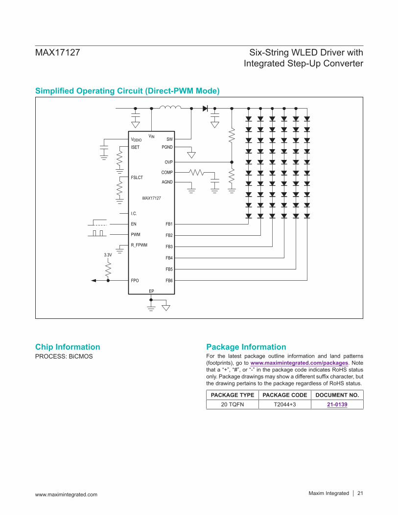
Simplified Operating Circuit appears at end of data sheet.
General DescriptionThe MAX17127 is a high-efficiency driver for white light-emitting diodes (LEDs). It is designed for large liquid-crystal displays (LCDs) that employ an array of LEDs as the light source. An internal switch current-mode step-up converter drives the LED array, which can be configured for up to six strings in parallel and 13 LEDs per string. Each string is terminated with ballast that achieves ±2% current-regulation accuracy, ensuring even LED bright-ness. The MAX17127 has a wide input voltage range from 5V to 26V, and provides adjustable 10mA to 30mA full-scale LED current.The MAX17127 can implement brightness control through the PWM signal input, and LED current is directly controlled by the external dimming signal’s frequency and duty cycle.The MAX17127 has multiple features to protect the controller from fault conditions. Once an open/short string is detected, the fault string is disabled while other strings can still operate normally. The controller features cycle-by-cycle current limit to provide constant operation and soft-start capability. If the MAX17127 is in current-limit condition, the step-up converter is latched off after an internal timer expires. A thermal-shutdown circuit pro-vides another level of protection. When thermal shutdown happens, the MAX17127 is latched off.The MAX17127’s step-up controller features an internal 0.12Ω (typ), 48V (max) power MOSFET with local current-sense amplifier for accurate cycle-by-cycle current limit. This architecture greatly simplifies the external circuitry and saves PCB space. Low-feedback voltage at each LED string helps reduce power loss and improve efficiency. The MAX17127 features resistor-adjustable switching frequency from 250kHz to 1MHz, which enables a wide variety of applications that can trade off component size for operating frequency.The MAX17127 is available in a thermally enhanced, lead-free, 20-pin, 4mm x 4mm thin QFN package.
Features 5V to 26V Input Supply Voltage Up to Six Parallel Strings Multiple Series-Connected
LEDs 250kHz to 1MHz Adjustable Switching Frequency 0.12Ω Internal HV Power MOSFET (48V max) Low String Feedback Voltage: 480mV at 20mA LED
Current Full-Scale LED Current Adjustable from 10mA to
30mA ±2% Current-Regulation Accuracy Between Strings 400ns Minimum String On-Time 100Hz to 25kHz PWM Input Range Open and Short LED Protection Output Overvoltage Protection Thermal Shutdown Small 20-Pin, 4mm x 4mm Thin QFN Package
Applications Notebook, Subnotebook, and Tablet Computer
Displays Handy Terminals
+Denotes a lead(Pb)-free/RoHS-compliant package.*EP = Exposed pad.
PART TEMP RANGE PIN-PACKAGEMAX17127ETP+ -40°C to +85°C 20 TQFN-EP*
MAX17127 Six-String WLED Driver with Integrated Step-Up Converter
19-5164; Rev 1; 11/14
Ordering Information
EVALUATION KIT AVAILABLE
VIN to AGND ........................................................-0.3V to +30VFB_, SW to PGND ................................................-0.3V to +52VPGND to AGND ....................................................-0.3V to +0.3VVDDIO, PWM, EN, FPO, I.C. to AGND ....................-0.3V to +6VCOMP, ISET, R_FPWM, OVP, FSLCT
to AGND .............................................. -0.3V to VDDIO + 0.3VSW Switch Maximum Continuous RMS Current ..................1.6AContinuous Power Dissipation (TA = +70°C) TQFN (derate 16.9mW/NC above +70°C) ................1349mW
Operating Temperature Range ........................... -40°C to +85°CJunction Temperature ......................................................+150°CStorage Temperature Range ............................ -60°C to +150°CESD HBM ...................................................................................2kV MM ...................................................................................200VLead Temperature (soldering, 10s) .................................+300°CSoldering Temperature (reflow) .......................................+260°C
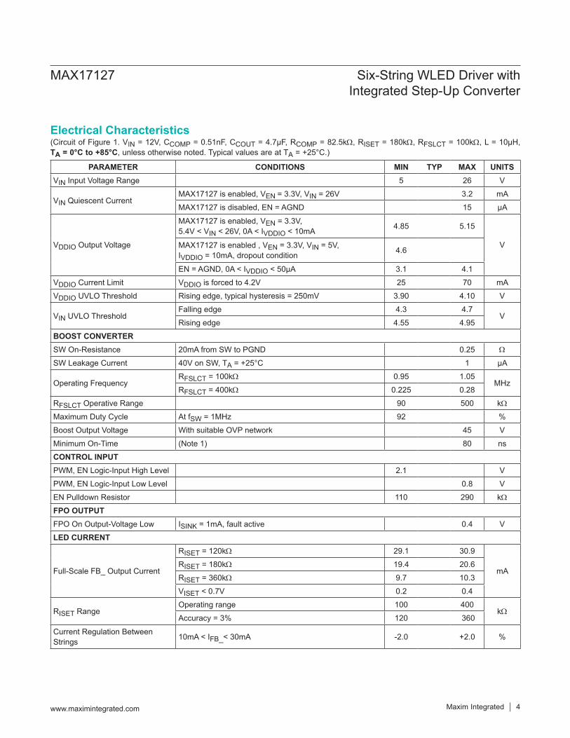
(Circuit of Figure 1. VIN = 12V, CCOMP = 0.51nF, CCOUT = 4.7µF, RCOMP = 82.5kΩ, RISET = 180kΩ, RFSLCT = 100kΩ, L = 10µH, TA = 0°C to +85°C, unless otherwise noted. Typical values are at TA = +25°C.)
PARAMETER CONDITIONS MIN TYP MAX UNITSVIN Input Voltage Range 5 26 V
VIN Quiescent CurrentMAX17127 is enabled, VEN = 3.3V, VIN = 26V 2.7 3.2 mA
MAX17127 is disabled, EN = AGND 5 10 µA
VDDIO Output Voltage
MAX17127 is enabled, VEN = 3.3V,5.4V < VIN < 26V, 0A < IVDDIO < 10mA 4.85 5 5.15
VMAX17127 is enabled, VEN = 3.3V, VIN = 5V, IVDDIO = 10mA,dropout condition 4.6 4.75
MAX17127 is disabled, EN = AGND, 0A < IVDDIO < 50µA 3.1 3.7 4.1 V
VDDIO Current Limit VDDIO is forced to 4.2V 25 45 70 mA
VDDIO UVLO Threshold Rising edge, typical hysteresis = 250mV 3.90 4.00 4.10 V
VIN UVLO ThresholdFalling edge 4.3 4.5 4.7
VRising edge 4.55 4.75 4.95
BOOST CONVERTERSW On-Resistance 20mA from SW to PGND 0.12 0.25 Ω
SW Leakage Current 40V on SW, TA = +25°C 1 µA
Operating FrequencyRFSLCT = 100kΩ 0.95 1.0 1.05
MHzRFSLCT = 400kΩ 0.225 0.25 0.275
RFSLCT Range Operating range 90 500 kΩ
Maximum Duty Cycle At fSW = 1MHz 91 95 %
Minimum On-Time (Note 1) 50 80 ns
SW Current Limit Duty cycle = 75% 3.12 3.9 4.7 A
CONTROL INPUTPWM, EN Logic-InputHigh Level 2.1 V
PWM, EN Logic-Input LowLevel 0.8 V
EN Pulldown Resistor 120 200 280 kΩ
www.maximintegrated.com Maxim Integrated 2
MAX17127 Six-String WLED Driver with Integrated Step-Up Converter
Electrical Characteristics
Stresses beyond those listed under “Absolute Maximum Ratings” may cause permanent damage to the device. These are stress ratings only, and functional operation of the device at these or any other conditions beyond those indicated in the operational sections of the specifications is not implied. Exposure to absolute maximum rating conditions for extended periods may affect device reliability.
Absolute Maximum Ratings
(Circuit of Figure 1. VIN = 12V, CCOMP = 0.51nF, CCOUT = 4.7µF, RCOMP = 82.5kΩ, RISET = 180kΩ, RFSLCT = 100kΩ, L = 10µH, TA = 0°C to +85°C, unless otherwise noted. Typical values are at TA = +25°C.)
PARAMETER CONDITIONS MIN TYP MAX UNITSFPO OUTPUTFPO Off-Leakage Current Fault inactive, TA = +25°C 100 nAFPO On Output-VoltageLow ISINK = 1mA, fault active 0.4 V
INPUT LEAKAGEPWM Leakage Current TA = +25NC, VPWM = 0V, VPWM = 5V -1 +1 µA
OVP Leakage Current TA = +25NC, VOVP = 0V, VOVP = 5V -0.1 +0.1 µA
LED CURRENT
Full-Scale FB_ OutputCurrent
RISET = 120kΩ 29.1 30 30.9
mARISET = 180kΩ 19.6 20 20.4RISET = 360kΩ 9.7 10 10.3VISET < 0.7V 0.2 0.3 0.4
RISET RangeOperating range 100 400
kΩAccuracy = 3% 120 360
Current RegulationBetween Strings 10mA < IFB_< 30mA -2.0 +2.0 %
Minimum FB_ RegulationVoltage
IFB_ = 30mA 400 555 770
mVIFB_ = 20mA 460 670
IFB_ = 10mA 350 630
FB_ On-Resistance VFB_ = 50mV (includes 10Ω sense resistor) 17.5 28.4 Ω
FB_ Bias Current VFB_ = 40V, TA = +25°C 0.1 1 µAFB_ Minimum On-Time 400 580 700 nsFAULT PROTECTIONOVP Threshold Voltage Rising edge, typical hysteresis = 90mV 1.23 1.25 1.27 VFB_ OvervoltageThreshold 7 8 9 V
FB_ Enable ThresholdVoltage 1.2 V
FB_ Open ThresholdVoltage 130 280 mV
FB_ Check LED SourceCurrent 0.4 1.3 mA
FB_ Check LED Time 0.7 1.0 1.3 ms
Thermal-ShutdownThreshold (Note 1) +150 °C
Overcurrent Fault Timer Latchoff timer 128 µsPWM CONTROLPWM Input On-Time 400 nsPWM Input FrequencyRange 0.1 25 kHz
www.maximintegrated.com Maxim Integrated 3
MAX17127 Six-String WLED Driver with Integrated Step-Up Converter
Electrical Characteristics (continued)
(Circuit of Figure 1. VIN = 12V, CCOMP = 0.51nF, CCOUT = 4.7µF, RCOMP = 82.5kΩ, RISET = 180kΩ, RFSLCT = 100kΩ, L = 10µH, TA = 0°C to +85°C, unless otherwise noted. Typical values are at TA = +25°C.)
PARAMETER CONDITIONS MIN TYP MAX UNITSVIN Input Voltage Range 5 26 V
VIN Quiescent CurrentMAX17127 is enabled, VEN = 3.3V, VIN = 26V 3.2 mA
MAX17127 is disabled, EN = AGND 15 μA
VDDIO Output Voltage
MAX17127 is enabled, VEN = 3.3V,5.4V < VIN < 26V, 0A < IVDDIO < 10mA 4.85 5.15
VMAX17127 is enabled , VEN = 3.3V, VIN = 5V,IVDDIO = 10mA, dropout condition 4.6
EN = AGND, 0A < IVDDIO < 50µA 3.1 4.1
VDDIO Current Limit VDDIO is forced to 4.2V 25 70 mA
VDDIO UVLO Threshold Rising edge, typical hysteresis = 250mV 3.90 4.10 V
VIN UVLO ThresholdFalling edge 4.3 4.7
VRising edge 4.55 4.95
BOOST CONVERTERSW On-Resistance 20mA from SW to PGND 0.25 Ω
SW Leakage Current 40V on SW, TA = +25°C 1 μA
Operating FrequencyRFSLCT = 100kΩ 0.95 1.05
MHzRFSLCT = 400kΩ 0.225 0.28
RFSLCT Operative Range 90 500 kΩ
Maximum Duty Cycle At fSW = 1MHz 92 %
Boost Output Voltage With suitable OVP network 45 V
Minimum On-Time (Note 1) 80 ns
CONTROL INPUTPWM, EN Logic-Input High Level 2.1 V
PWM, EN Logic-Input Low Level 0.8 V
EN Pulldown Resistor 110 290 kΩ
FPO OUTPUTFPO On Output-Voltage Low ISINK = 1mA, fault active 0.4 V
LED CURRENT
Full-Scale FB_ Output Current
RISET = 120kΩ 29.1 30.9
mARISET = 180kΩ 19.4 20.6
RISET = 360kΩ 9.7 10.3
VISET < 0.7V 0.2 0.4
RISET RangeOperating range 100 400
kΩAccuracy = 3% 120 360
Current Regulation BetweenStrings 10mA < IFB_< 30mA -2.0 +2.0 %
www.maximintegrated.com Maxim Integrated 4
MAX17127 Six-String WLED Driver with Integrated Step-Up Converter
Electrical Characteristics
(Circuit of Figure 1. VIN = 12V, TA = +25°C, unless otherwise noted.)
Note 1: Specifications are guaranteed by design, not production tested.
(Circuit of Figure 1. VIN = 12V, CCOMP = 0.51nF, CCOUT = 4.7µF, RCOMP = 82.5kΩ, RISET = 180kΩ, RFSLCT = 100kΩ, L = 10µH, TA = 0°C to +85°C, unless otherwise noted. Typical values are at TA = +25°C.)
PARAMETER CONDITIONS MIN TYP MAX UNITS
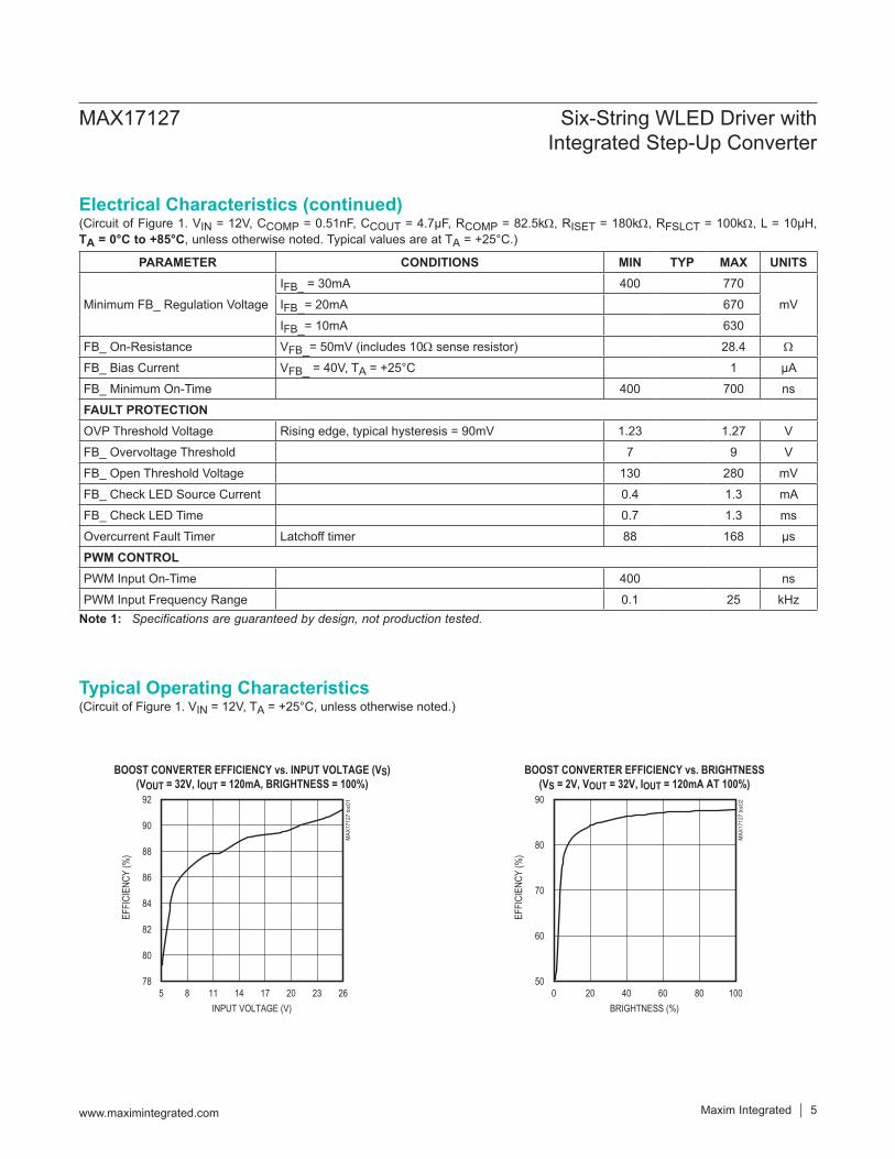
Minimum FB_ Regulation Voltage
IFB_ = 30mA 400 770
mVIFB_= 20mA 670
IFB_= 10mA 630
FB_ On-Resistance VFB_= 50mV (includes 10Ω sense resistor) 28.4 Ω
FB_ Bias Current VFB_ = 40V, TA = +25°C 1 μA
FB_ Minimum On-Time 400 700 ns
FAULT PROTECTIONOVP Threshold Voltage Rising edge, typical hysteresis = 90mV 1.23 1.27 V
FB_ Overvoltage Threshold 7 9 V
FB_ Open Threshold Voltage 130 280 mV
FB_ Check LED Source Current 0.4 1.3 mA
FB_ Check LED Time 0.7 1.3 ms
Overcurrent Fault Timer Latchoff timer 88 168 μs
PWM CONTROLPWM Input On-Time 400 ns
PWM Input Frequency Range 0.1 25 kHz
BOOST CONVERTER EFFICIENCY vs. BRIGHTNESS(VS = 2V, VOUT = 32V, IOUT = 120mA AT 100%)
MAX
1712
7 to
c02
BRIGHTNESS (%)
EFFI
CIEN
CY (%
)
80604020
60
70
80
90
500 100
BOOST CONVERTER EFFICIENCY vs. INPUT VOLTAGE (VS)(VOUT = 32V, IOUT = 120mA, BRIGHTNESS = 100%)
MAX
1712
7 to
c01
INPUT VOLTAGE (V)
EFFI
CIEN
CY (%
)
23201714118
80
82
84
86
88
90
92
785 26
www.maximintegrated.com Maxim Integrated 5
MAX17127 Six-String WLED Driver with Integrated Step-Up Converter
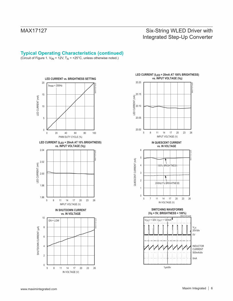
Typical Operating Characteristics
Electrical Characteristics (continued)
(Circuit of Figure 1. VIN = 12V, TA = +25°C, unless otherwise noted.)
SWITCHING WAVEFORMS(VS = 5V, BRIGHTNESS = 100%)
MAX17127 toc08
1µs/div
VLX20V/div
0mA
500mA/div
INDUCTORCURRENT
0V
VOUT = 32V, IOUT = 120mA
IN SHUTDOWN CURRENTvs. IN VOLTAGE
MAX
1712
7 to
c07
IN VOLTAGE (V)
SHUT
DOW
N CU
RREN
T (µ
A)
23201714118
2
4
6
8
10
05 26
EN = LOW
IN QUIESCENT CURRENTvs. IN VOLTAGE
MAX
1712
7 to
c06
IN VOLTAGE (V)
QUIE
SCEN
T CU
RREN
T (m
A)
23201714117
1
2
3
4
5
6
05 26
100% BRIGHTNESS
200Hz/1% BRIGHTNESS
LED CURRENT (ILED = 20mA AT 10% BRIGHTNESS)vs. INPUT VOLTAGE (VS)
MAX
1712
7 to
c05
INPUT VOLTAGE (V)
LED
CURR
ENT
(mA)
23201714118
1.98
2.00
2.02
2.04
1.965 26
LED CURRENT (ILED = 20mA AT 100% BRIGHTNESS)vs. INPUT VOLTAGE (VS)
MAX
1712
7 to
c04
INPUT VOLTAGE (V)LE
D CU
RREN
T (m
A)23201714118
20.05
20.10
20.15
20.20
20.005 26
LED CURRENT vs. BRIGHTNESS SETTING
MAX
1712
7 to
c03
PWM DUTY CYCLE (%)
LED
CURR
ENT
(mA)
80604020
5
10
15
20
00 100
fPWM = 200Hz
Maxim Integrated 6www.maximintegrated.com
MAX17127 Six-String WLED Driver with Integrated Step-Up Converter
Typical Operating Characteristics (continued)
(Circuit of Figure 1. VIN = 12V, TA = +25°C, unless otherwise noted.)
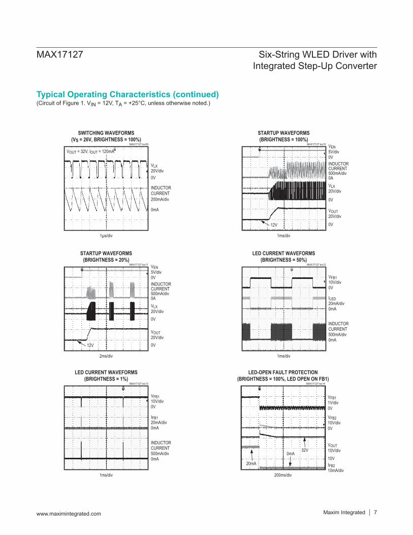
LED-OPEN FAULT PROTECTION(BRIGHTNESS = 100%, LED OPEN ON FB1)
MAX17127 toc14
200ms/div
VOUT10V/div
VFB11V/div0V
VFB210V/div0V
IFB210mA/div
10V20mA
0mA32V
LED CURRENT WAVEFORMS(BRIGHTNESS = 1%)
MAX17127 toc13
1ms/div
VFB110V/div0V
INDUCTORCURRENT500mA/div0mA
IFB120mA/div0mA
LED CURRENT WAVEFORMS(BRIGHTNESS = 50%)
MAX17127 toc12
1ms/div
VFB110V/div0V
INDUCTORCURRENT500mA/div0mA
ILED20mA/div0mA
STARTUP WAVEFORMS(BRIGHTNESS = 20%)
MAX17127 toc11
2ms/div
VLX20V/div
VOUT20V/div
VEN5V/div
0V
INDUCTORCURRENT500mA/div0A
0V
0V
12V
STARTUP WAVEFORMS(BRIGHTNESS = 100%)
MAX17127 toc10
1ms/div
VLX20V/div
VOUT20V/div
VEN5V/div
0V
INDUCTORCURRENT500mA/div0A
0V
0V
12V
SWITCHING WAVEFORMS(VS = 26V, BRIGHTNESS = 100%)
MAX17127 toc09
1µs/div
VLX20V/div
0mA
200mA/div
INDUCTORCURRENT
0V
VOUT = 32V, IOUT = 120mA
Maxim Integrated 7www.maximintegrated.com
MAX17127 Six-String WLED Driver with Integrated Step-Up Converter
Typical Operating Characteristics (continued)
(Circuit of Figure 1. VIN = 12V, TA = +25°C, unless otherwise noted.)
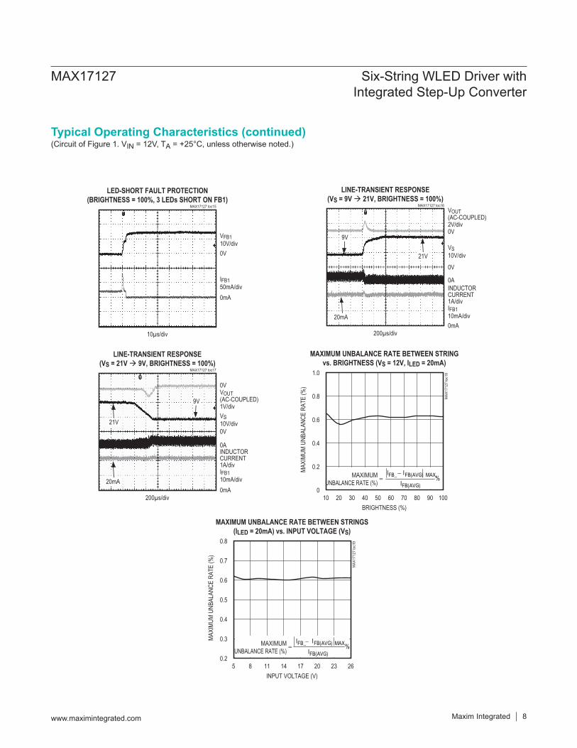
MAXIMUM UNBALANCE RATE BETWEEN STRINGS(ILED = 20mA) vs. INPUT VOLTAGE (VS)
MAX
1712
7 to
c19
INPUT VOLTAGE (V)
MAXI
MUM
UNBA
LANC
E RA
TE (%
)
23201714118
0.3
0.4
0.5
0.6
0.7
0.8
0.25 26
MAXIMUMUNBALANCE RATE (%)
−= FB_ FB(AVG) MAX
FB(AVG)
I I%
I
MAXIMUM UNBALANCE RATE BETWEEN STRINGvs. BRIGHTNESS (VS = 12V, ILED = 20mA)
MAX
1712
7 to
c18
BRIGHTNESS (%)
MAXI
MUM
UNBA
LANC
E RA
TE (%
)
80 90706050403020
0.2
0.4
0.6
0.8
1.0
010 100
MAXIMUMUNBALANCE RATE (%)
−= FB_ FB(AVG) MAX
FB(AVG)
I I%
I
LINE-TRANSIENT RESPONSE(VS = 21V 9V, BRIGHTNESS = 100%)
MAX17127 toc17
200µs/div
IFB110mA/div
0VVOUT(AC-COUPLED)1V/divVS10V/div0V
0mA
0AINDUCTORCURRENT1A/div
20mA
9V
21V
LINE-TRANSIENT RESPONSE(VS = 9V 21V, BRIGHTNESS = 100%)
MAX17127 toc16
200µs/div
IFB110mA/div
VOUT(AC-COUPLED)2V/div0V
VS10V/div
0mA
0AINDUCTORCURRENT1A/div
20mA
9V
21V0V
LED-SHORT FAULT PROTECTION(BRIGHTNESS = 100%, 3 LEDs SHORT ON FB1)
MAX17127 toc15
10µs/div
VFB110V/div
IFB150mA/div0mA
0V
Maxim Integrated 8www.maximintegrated.com
MAX17127 Six-String WLED Driver with Integrated Step-Up Converter
Typical Operating Characteristics (continued)
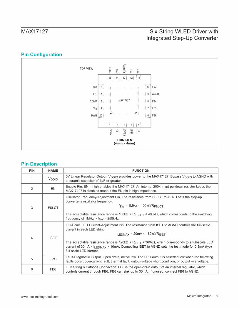
PIN NAME FUNCTION
1 VDDIO5V Linear Regulator Output. VDDIO provides power to the MAX17127. Bypass VDDIO to AGND witha ceramic capacitor of 1µF or greater.
2 EN Enable Pin. EN = high enables the MAX17127. An internal 200kI (typ) pulldown resistor keeps theMAX17127 in disabled mode if the EN pin is high impedance.
3 FSLCT
Oscillator Frequency-Adjustment Pin. The resistance from FSLCT to AGND sets the step-upconverter’s oscillator frequency:
fSW = 1MHz × 100kΩ/RFSLCT
The acceptable resistance range is 100kΩ < RFSLCT < 400kΩ, which corresponds to the switchingfrequency of 1MHz > fSW > 250kHz.
4 ISET
Full-Scale LED Current-Adjustment Pin. The resistance from ISET to AGND controls the full-scalecurrent in each LED string:
ILEDMAX = 20mA × 180kΩ/RISET
The acceptable resistance range is 120kΩ < RISET < 360kΩ, which corresponds to a full-scale LEDcurrent of 30mA > ILEDMAX > 10mA. Connecting ISET to AGND sets the test mode for 0.3mA (typ)full-scale LED current.
5 FPO Fault-Diagnostic Output. Open drain, active low. The FPO output is asserted low when the followingfaults occur: overcurrent fault, thermal fault, output-voltage short condition, or output overvoltage.
6 FB6 LED String 6 Cathode Connection. FB6 is the open-drain output of an internal regulator, whichcontrols current through FB6. FB6 can sink up to 30mA. If unused, connect FB6 to AGND.
19
20
18
17
7
6
8
EN FPO
9
V DDI
O
OVP
FB1
FB2
PGND
1 2
COMP
4 5
15 14 12 11
VIN
PWM + EP
AGND
FB4
FB5
FB6
FSLC
TR_
FPW
M3
13
I.C.
16 10 FB3SW
THIN QFN(4mm × 4mm)
TOP VIEW
ISET
MAX17127
www.maximintegrated.com Maxim Integrated 9
MAX17127 Six-String WLED Driver with Integrated Step-Up Converter
Pin Description
Pin Configuration
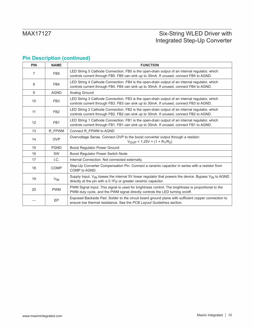
PIN NAME FUNCTION
7 FB5 LED String 5 Cathode Connection. FB5 is the open-drain output of an internal regulator, whichcontrols current through FB5. FB5 can sink up to 30mA. If unused, connect FB5 to AGND.
8 FB4 LED String 4 Cathode Connection. FB4 is the open-drain output of an internal regulator, whichcontrols current through FB4. FB4 can sink up to 30mA. If unused, connect FB4 to AGND.
9 AGND Analog Ground
10 FB3 LED String 3 Cathode Connection. FB3 is the open-drain output of an internal regulator, whichcontrols current through FB3. FB3 can sink up to 30mA. If unused, connect FB3 to AGND.
11 FB2 LED String 2 Cathode Connection. FB2 is the open-drain output of an internal regulator, whichcontrols current through FB2. FB2 can sink up to 30mA. If unused, connect FB2 to AGND.
12 FB1 LED String 1 Cathode Connection. FB1 is the open-drain output of an internal regulator, whichcontrols current through FB1. FB1 can sink up to 30mA. If unused, connect FB1 to AGND.
13 R_FPWM Connect R_FPWM to AGND
14 OVP Overvoltage Sense. Connect OVP to the boost converter output through a resistor:VOVP = 1.25V × (1 + R1/R2)
15 PGND Boost Regulator Power Ground
16 SW Boost Regulator Power Switch Node
17 I.C. Internal Connection. Not connected externally.
18 COMP Step-Up Converter Compensation Pin. Connect a ceramic capacitor in series with a resistor from COMP to AGND.
19 VINSupply Input. VIN biases the internal 5V linear regulator that powers the device. Bypass VIN to AGND directly at the pin with a 0.1Fµ or greater ceramic capacitor.
20 PWM PWM Signal Input. This signal is used for brightness control. The brightness is proportional to the PWM duty cycle, and the PWM signal directly controls the LED turning on/off.
— EP Exposed Backside Pad. Solder to the circuit board ground plane with sufficient copper connection to ensure low thermal resistance. See the PCB Layout Guidelines section.
www.maximintegrated.com Maxim Integrated 10
MAX17127 Six-String WLED Driver with Integrated Step-Up Converter
Pin Description (continued)
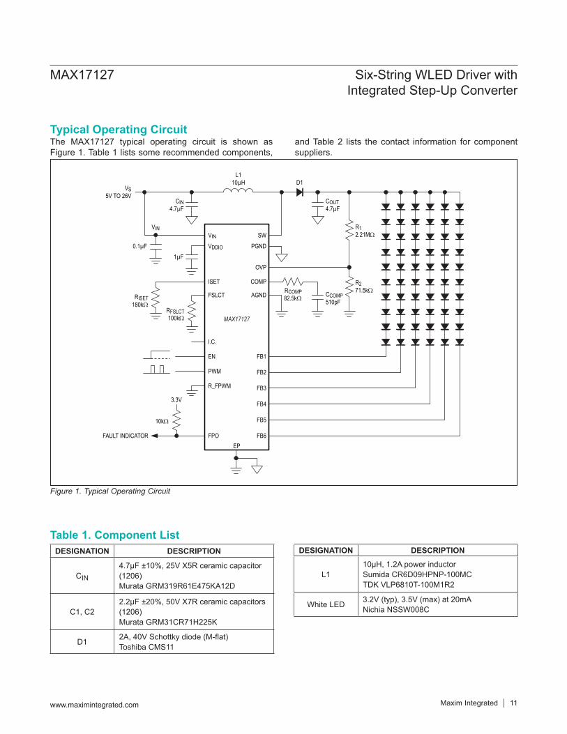
The MAX17127 typical operating circuit is shown as Figure 1. Table 1 lists some recommended components,
and Table 2 lists the contact information for component suppliers.
Table 1. Component List
Figure 1. Typical Operating Circuit
DESIGNATION DESCRIPTION
L110μH, 1.2A power inductorSumida CR6D09HPNP-100MCTDK VLP6810T-100M1R2
White LED 3.2V (typ), 3.5V (max) at 20mANichia NSSW008C
DESIGNATION DESCRIPTION
CIN
4.7μF ±10%, 25V X5R ceramic capacitor(1206)Murata GRM319R61E475KA12D
C1, C22.2μF ±20%, 50V X7R ceramic capacitors(1206)Murata GRM31CR71H225K
D1 2A, 40V Schottky diode (M-flat)Toshiba CMS11
EP
SWVIN
PGND0.1µF
VS5V TO 26V
FAULT INDICATOR
VIN
L110µH D1
R12.21MΩ
OVP
COMP
AGND
FB1
FB3
FB4
FB5
FB6
VDDIO
1µF
RFSLCT100kΩ
RCOMP82.5kΩ CCOMP
510pF
CIN4.7µF
COUT4.7µF
ISET
EN
PWM
FSLCT
FB2
R_FPWM
FPO
3.3V
RISET180kΩ
10kΩ
I.C.
R271.5kΩ
MAX17127
www.maximintegrated.com Maxim Integrated 11
MAX17127 Six-String WLED Driver with Integrated Step-Up Converter
Typical Operating Circuit

Figure 2. Functional Diagram
Table 2. Component SuppliersSUPPLIER PHONE WEBSITE
Murata Electronics North America, Inc. 770-436-1300 www.murata.com
Nichia Corp. 248-352-6575 www.nichia.com
Sumida Corp. 847-545-6700 www.sumida.com
Toshiba America Electronic Components, Inc. 949-455-2000 www.toshiba.com/taec
Vishay 203-268-6261 www.vishay.com
Gm1.25V
CLAMP
5V LINEAR REGULATOR
OVP
VIN
VDDIO
FSLCT
COMP
ISET
EN
ERRORAMPLIFIER
ERRORAMPLIFIER
VDDIO
EN
OSCILLATOR
ISET
CURRENTSENSE
CONTROLAND
DRIVERLOGIC
CURRENT SOURCE
PGND
AGND
FB2
FB1
SW
OVP
1.25V
8V
PWM PWM CONTROL
FAULTCONTROL
ΣSLOPECOMPENSATION
OVERVOLTAGECOMPARATOR
VSAT
TO FAULTCONTROL
FAULTCONTROL
ERRORCOMPARATOR
N
N
Gm
HVC
S&H
LVC
FB6FB5FB4
FB2FB3
CURRENT SOURCE FB3
CURRENT SOURCE FB4
CURRENT SOURCE FB5
CURRENT SOURCE FB6
EN
R_FPWM
I.C. VDDIO
FPO
MAX17127
www.maximintegrated.com Maxim Integrated 12
MAX17127 Six-String WLED Driver with Integrated Step-Up Converter
Detailed DescriptionThe MAX17127 is a high-efficiency driver for arrays of white LEDs. It contains a fixed-frequency current-mode PWM step-up controller, a 5V linear regulator, a dimming control circuit, an internal power MOSFET, and six regulated current sources. Figure 2 shows the MAX17127 functional diagram. When enabled, the step-up controller boosts the output voltage to provide sufficient headroom for the current sources to regu-late their respective string currents. The MAX17127 features resistor-adjustable switching frequency (250kHz to 1MHz), which allows trade-offs between external component size and operating efficiency.The MAX17127 can implement brightness control through the PWM signal input. The LED current is directly controlled by the external dimming signal's frequency and duty cycle.The MAX17127 has multiple features to protect the controller from fault conditions. Separate feedback loops limit the output voltage in all circumstances. The MAX17127 checks each FB_ voltage during operation.If one or more strings are open, the corresponding FB_ voltages are pulled below 180mV (max), and an open-circuit fault is detected. As a result, the respective current sources are disabled.When one or more LEDs are shorted and the related FB_ voltage exceeds 8V, short fault is detected and the respective current source is disabled if at least one FB_ voltage is lower than the minimum FB_ regulation voltage +460mV (typ).When in LED open or short conditions, the fault string is disabled while other strings can still operate normally.The MAX17127 also includes other kinds of fault protections, which are overcurrent, thermal shutdown, and output overvoltage. The MAX17127 features cycle-by-cycle current limit to provide consistent operation and soft-start protection. In an overcurrent condition, the IC latches off if the fault still exists after a 128µs overcurrent fault timer expires. The output overvoltage is a nonlatched operation, and the step-up converter stops switching during the fault. A thermal-shutdown circuit provides another level of protection. The MAX17127 is latched off once thermal shutdown occurs.The MAX17127 includes a 5V linear regulator that provides the internal bias and gate driver for the step-up controller.
Fixed-Frequency Step-Up ControllerThe MAX17127’s fixed-frequency, current-mode, step-up controller automatically chooses the lowest active FB_ voltage to regulate the feedback voltage. Specifically, the difference between the lowest FB_ voltage and the current source control signal plus an offset is integrated at the COMP output. The resulting error signal is compared to the internal switch current plus slope compensation to determine the switch on-time. As the load changes, the error amplifier sources or sinks current to the COMP output to deliver the required peak inductor current. The slope-compensation signal is added to the current-sense signal in order to improve stability at high duty cycles.
Internal 5V Linear Regulator and UVLOThe MAX17127 includes an internal low-dropout linear regulator (VDDIO). When VIN is higher than 5.0V, this linear regulator generates a 5V supply to power the internal PWM controller, control logic, and MOSFET driver. The VDDIO voltage drops to 3.3V in shutdown. If 5V < VIN < 5.5V, VDDIO and VIN can be connected together and powered from an external 5V supply. There is a body diode from VDDIO to VIN, so VIN must be greater than VDDIO (see Figure 2).The MAX17127 is disabled until VDDIO exceeds the UVLO threshold. The hysteresis on UVLO is approxi-mately 250mV. In standby mode, the internal LDO is in low-power mode with 10µA (max) input current and approximately regulated at 3.3V (typ). When EN = high, the internal LDO is enabled and regulated accurately at 5V (typ).The VDDIO pin should be bypassed to AGND with a minimum 1µF ceramic capacitor.
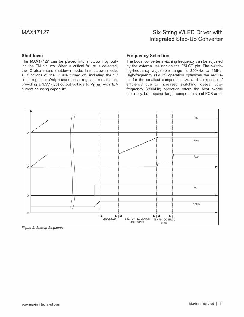
StartupAt startup, the MAX17127 performs a diagnostic test of the LED array. In the test phase, all FB_ pins are pulled up by a given current source (0.4mA min) during 1ms (typ). If some FB_ voltage is lower than 1.2V (max), the string is considered to be unused. Therefore, when a string is not in use, it should be connected to AGND. All other strings with FB_ higher than 1.2V (max) are detected as in use. After the LED string diagnostic phases are finished, the boost converter starts. An additional 1ms after boost soft-start end is used as minimum FB_ control. The total startup time is less than 10ms, including 2ms (typ) soft-start. Figure 3 shows the sequence.
www.maximintegrated.com Maxim Integrated 13
MAX17127 Six-String WLED Driver with Integrated Step-Up Converter
ShutdownThe MAX17127 can be placed into shutdown by pull-ing the EN pin low. When a critical failure is detected, the IC also enters shutdown mode. In shutdown mode, all functions of the IC are turned off, including the 5V linear regulator. Only a crude linear regulator remains on, providing a 3.3V (typ) output voltage to VDDIO with 1µA current-sourcing capability.
Frequency SelectionThe boost converter switching frequency can be adjusted by the external resistor on the FSLCT pin. The switch-ing-frequency adjustable range is 250kHz to 1MHz. High-frequency (1MHz) operation optimizes the regula-tor for the smallest component size at the expense of efficiency due to increased switching losses. Low-frequency (250kHz) operation offers the best overall efficiency, but requires larger components and PCB area.
Figure 3. Startup Sequence
MIN FB_ CONTROL(1ms)
VDDIO
VOUT
VEN
CHECK LED
VIN
0V
0V
0V
0V
ILED
STEP-UP REGULATORSOFT-START
www.maximintegrated.com Maxim Integrated 14
MAX17127 Six-String WLED Driver with Integrated Step-Up Converter
Overvoltage ProtectionTo protect the step-up regulator when the load is open, or if the output voltage becomes excessive for any reason, the MAX17127 features a dedicated overvoltage- feedback input (OVP). The OVP pin is connected to the center tap of a resistive voltage-divider from the high- voltage output. When the OVP pin voltage (VOVP) exceeds 1.25V (typ), a comparator turns off the internal power MOSFET. This step-up regulator switch is reenabled after the VOVP drops 90mV (typ hyster-esis) below the protection threshold. This overvoltage- protection feature ensures the step-up regulator fail-safe operation when the LED strings are disconnected from the output.
LED Current SourcesMaintaining uniform LED brightness and dimming capability is critical for backlight applications. The MAX17127 is equipped with a bank of six matched current sources. These specialized current sources are accurate within ≤ 3% and match each other within 2%. They can be switched on and off at PWM frequencies of up to 25kHz. LED full-scale current is set through the ISET pin (10mA < ILED < 30mA).The minimum voltage drop across each current source is 480mV (typ) when the LED current is 20mA. The low-voltage drop helps reduce dissipation while maintaining sufficient compliance to control the LED current within the required tolerances.The LED current sources can be disabled by connecting the respective FB_ pin to AGND at startup. When the IC is enabled, the controller scans settings for all FB_ pins. If an FB_ pin is not connected to AGND, an internal circuit pulls this pin high, and the controller enables the corresponding current source to regulate the string current. If the FB_ pin is connected to AGND, the controller disables the corresponding current regulator. The current regulator cannot be disabled by connecting the respective FB_ pin to AGND after the IC is enabled.All FB_ pins in use are combined to extract a lowest FB_ voltage (LVC) (see Figure 2). LVC is fed into the step-up regulator’s error amplifier and is used to set the output voltage.
Current-Source Fault ProtectionLED fault open/short is detected after startup. When one or more strings fail after startup, the corresponding current source is disabled. The remaining LED strings are still operated normally. The LED open/short detection is not executed when LED on-time is less than 2µs.The MAX17127 can tolerate a slight mismatch between LED strings. When severe mismatches or WLED shorts occur, the FB_ voltages are uneven because of mismatched voltage drops across strings. At each LED turn-on, the FB_ voltage is brought down to the regulation voltage quickly. When FB_ voltage is higher than 8V (typ) after LED turn-on, an LED short is detected if at least one FB_ voltage is lower than the minimum FB_ regulation voltage, +460mV (typ). The remaining LED strings can still operate normally. The LED short protection is dis-abled during the soft-start phase of the step-up regulator.
Open Current-Source ProtectionThe MAX17127 step-up regulator output voltage is regulated according to the minimum FB_ voltages on all the strings in use. If one or more strings are open, the respective FB_ pins are pulled to ground. For any FB_ lower than 180mV, the corresponding current source is disabled. The remaining LED strings can still operate normally. If all strings in use are open, the MAX17127 shuts the step-up regulator down.
FPO FunctionThe fault conditions trigger FPO function and pull the FPO pin low. Table 3 shows the state of the FPO pin with different fault conditions.
Dimming ControlThe MAX17127 performs brightness control with a PWM input signal. Dimming duty cycle and frequency of current sources follow the signal at the PWM pin directly.
Table 3. FPO Function TableFAULT CONDITION
THERMAL FAULT OUTPUT OVERVOLTAGE INPUT OVERCURRENTLATCHED Yes No (stop switching) Yes (after time expires)
FPO PIN STATE Low Low Low
www.maximintegrated.com Maxim Integrated 15
MAX17127 Six-String WLED Driver with Integrated Step-Up Converter
Full-Scale and Low-Level LED CurrentThe full-scale LED current is set by:
LED_MAXISET
20mA 180kIR× Ω
=
The acceptable resistance range for ISET is 120kΩ < RISET < 360kΩ, which corresponds to full-scale LED current of 30mA > ILED_MAX > 10mA.
Thermal ShutdownThe MAX17127 includes a thermal-protection circuit. When the local IC temperature exceeds +150°C (typ), the controller and current sources shut down. When the thermal shutdown happens, the FPO output pin is asserted low. The controller and current sources do not restart until the next enable signal is sent or input supply is recycled.
Design ProcedureAll MAX17127 designs should be prototyped and tested prior to production.External component-value choice is primarily dictated by the output voltage and the maximum load current, as well as maximum and minimum input voltages. Begin by selecting an inductor value. Once the inductor is known, choose the diode and capacitors.
Step-Up Converter Current CalculationTo ensure stable operation, the MAX17127 includes slope compensation, which sets the minimum inductor value. In continuous-conduction mode (CCM), the minimum inductor value is calculated with the following equation:
( )OUT(MAX) DIODE IN(MIN) SCCM(MIN)
SW(MIN)
V V 2 V RL
2 SF f
+ − × ×=
× ×
where:
IN
ININ
SF 72mV, when V 12.5V72mVSF , when V 12.5VV 12.5V1
10.6V
= < = >
− +
SF is a scale factor from the slope compensation depending on input voltage (this allows a higher current capability), the LCCM(MIN) is the minimum inductor value for stable operation in CCM, and RS = 15mΩ (typ) is the equivalent sensing scale factor from the controller’s internal current-sense circuit.
The controller can also operate in discontinuous- conduction mode (DCM). In this mode, the inductor value can be lower, but the peak inductor current is higher than in CCM. In DCM, the maximum inductor value is calculated with the following equation:
IN(MIN)DCM(MAX)
OUT(MAX) DIODE2
IN(MIN)
SW(MAX) OUT(MAX) OUT(MAX)
VL 1
V V
V2 f V I
= − +
× η×
× × ×
where the LDCM(MAX) is the maximum inductor value for DCM, η is the nominal regulator efficiency (85%), and IOUT(MAX) is the maximum output current.The output current capability of the step-up regulator is a function of current limit, input voltage, operating frequency, and inductor value. Because the slope compensation is used to stabilize the feedback loop, the inductor current limit depends on the duty cycle, and is determined with the following equation:
LIMS
LIMS
SFI 0.97, when D 30%R
SFI (1.27-D), when D 30%R
= × < = × >
where SF is the scale factor from the slope compensation, 2.5A is the current limit specified at 75% duty cycle, and D is the duty cycle.The output current capability depends on the current-limit value and operating mode. The maximum output current in CCM is governed by the following equation:
IN INOUT_CCM(MAX) LIM
SW OUT
0.5 D V VI If L V
× ×= − × × η
×
where ILIM is the current limit calculated above, η is the nominal regulator efficiency (85%), and D is the duty cycle. The corresponding duty cycle for this current is:
OUT IN DIODEOUT LIM ON DIODE
V V VDV I R V
− +=
− × +
where VDIODE is the forward voltage of the rectifier diode and RON is the internal MOSFET’s on-resistance (0.2Ω typ).
www.maximintegrated.com Maxim Integrated 16
MAX17127 Six-String WLED Driver with Integrated Step-Up Converter
The maximum output current in DCM is governed by the following equation:
( )( )
2LIM SW OUT DIODE
OUT_DCM(MAX)OUT OUT DIODE IN
L I f V VI
2 V V V V× × × η× +
=× × + −
Inductor SelectionThe inductance, peak current rating, series resistance, and physical size should all be considered when selecting an inductor. These factors affect the converter’s operating mode, efficiency, maximum output load capability, transient response time, output voltage ripple, and cost. The maximum output current, input voltage, output voltage, and switching frequency determine the inductor value. Very high inductance minimizes the current ripple, and therefore reduces the peak current, which decreases core losses in the inductor and I2R losses in the entire power path. However, large inductor values also require more energy storage and more turns of wire, which increase physical size and I2R copper losses. Low inductor values decrease the physical size but increase the current ripple and peak current. Finding the best inductor involves compromises among circuit efficiency, inductor size, and cost.In choosing an inductor, the first step is to determine the operating mode: continuous-conduction mode (CCM) or discontinuous-conduction mode (DCM). The MAX17127 has a fixed internal-slope compensation, which requires a minimum inductor value. When CCM is chosen, the ripple current and the peak current of the inductor can be minimized. If a small-size inductor is required, DCM can be chosen. In DCM, the inductor value and size can be minimized, but the inductor ripple current and peak current are higher than those in CCM. The controller can be stable, independent of the internal slope-compensation mode, but there is a maximum inductor-value requirement to ensure the DCM operating mode.The equations used here include a constant LIR, which is the ratio of the inductor peak-to-peak ripple current to the average DC inductor current at the full-load current. The controller operates in DCM mode when LIR is higher than 2.0, and it works in CCM mode when LIR is lower than 2.0. The best trade-off between inductor size and converter efficiency for step-up regulators generally has an LIR between 0.3 and 0.5. However, depending on the AC characteristics of the inductor core material and ratio
of inductor resistance to other power-path resistances, the best LIR can shift up or down. If the inductor resistance is relatively high, more ripples can be accepted to reduce the number of required turns and increase the wire diameter. If the inductor resistance is relatively low, increasing inductance to lower the peak current can reduce losses throughout the power path. If extremely thin high-resistance inductors are used, as is common for LCD panel applications, LIR higher than 2.0 can be chosen for DCM operating mode.Once a physical inductor is chosen, higher and lower values of the inductor should be evaluated for efficiency improvements in typical operating regions. The detailed design procedure for CCM can be described as follows: Calculate the approximate inductor value using the typical input voltage (VIN), the maximum output current (IOUT(MAX)), the expected efficiency (ηTYP) taken from an appropriate curve in the Typical Operating Characteristics, and an estimate of LIR based on the above discussion:
2IN(MIN) OUT IN(MIN) TYP
OUT OUT(MAX) SW
V V VL
V I f LIR
− η = ×
The MAX17127 has a minimum inductor-value limitation for stable operation in CCM operating mode at low input voltage because of the internal fixed-slope compensation. The minimum inductor value for stability is calculated with the following equation:
( )OUT(MAX) DIODE IN(MIN) SCCM(MIN)
SW(MIN)
V V 2 V RL
2 SF f
+ − × ×=
× ×
where SF is a scale factor from slope compensation, and RS is the equivalent current-sensing scale factor (15mΩ typ).Choose an available inductor value from an appropri-ate inductor family. Calculate the maximum DC input current at the minimum input voltage VIN(MIN), using conservation of energy and the expected efficiency at that operating point (ηMIN) taken from an appropriate curve in the Typical Operating Characteristics:
OUT(MAX) OUTIN(DC,MAX)
IN(MIN) MIN
I VI
V×
=× η
www.maximintegrated.com Maxim Integrated 17
MAX17127 Six-String WLED Driver with Integrated Step-Up Converter
Calculate the ripple current at that operating point and the peak current required for the inductor:
( )IN(MIN) OUT(MAX) IN(MIN)RIPPLE
OUT(MAX) SW
RIPPLEPEAK IN(DC,MAX)
V V VI
L V f
II I2
× −=
× ×
= +
When DCM operating mode is chosen to minimize the inductor value, the calculations are different from those above in CCM operating mode. The maximum inductor value for DCM mode is calculated with the following equation:
IN(MIN)DCM(MAX)
OUT(MAX) DIODE2
IN(MIN)
SW(MAX) OUT(MAX) OUT(MAX)
VL 1
V V
V2 f V I
= − +
× η×
× × ×
The peak inductor current in DCM is calculated with the following equation:
( )( )
OUT(MAX) OUT(MAX)
OUT(MAX) DIODE IN(MIN)PEAK
SW(MIN) OUT(MAX) DIODE
I 2 V
V V VI
L f V V
× ×
× + −=
× × η× +
The inductor’s saturation current rating should exceed IPEAK, and the inductor’s DC current rating should exceed IIN(DC,MAX). For good efficiency, choose an inductor with less than 0.1Ω series resistance.Considering the circuit with six 10-LED strings and 20mA LED full-scale current, the maximum load current (IOUT(MAX)) is 120mA with a 32V output and a minimal input voltage of 7V.Choosing a CCM operating mode with LIR = 0.7 at 1MHz and estimating efficiency of 85% at this operating point:
27V 32V 7V 0.85L 12.1 H32V 120mA 1MHz 0.7
− = = µ ×
In CCM, the inductor has to be higher than LCCM(MIN):
( )CCM(MIN)
32V 0.4V 2 7V 13.7mL 5.5 H
2 25.5mV 0.9MHz+ − × × Ω
= = µ× ×
A 10µH inductor is chosen, which is higher than the minimum L that guarantees stability in CCM.The peak inductor current at minimum input voltage is calculated as follows:
( )PEAK
7V 32V 7V120mA 32VI 0.95A7V 0.85 2 10 H 32V 0.9MHz
× −×= + =
× × µ × ×
Alternatively, choose a DCM operating mode by using lower inductance and estimating efficiency of 85% at this operating point. Since DCM has higher peak inductor current at lower input, it causes current limit when the parameters are not chosen properly. Considering the case with six 10-LED strings and 20mA LED full-scale current to prevent excessive switch current from causing current limit:
DCM(MAX)
2
7VL 132V 0.4V
(7V) 0.85 3.9 H2 1.1MHz 32V 120mA
= − +
×× = µ
× × ×
A 3.3µH inductor is chosen. The peak inductor current at minimum input voltage is calculated as follows:
( )( )PEAK
120mA 2 32V 32V 0.4V 7VI 1.40A
3.3 H 1.1MHz 0.85 32V 0.4V× × × + −
= =µ × × × +
Output Capacitor SelectionThe total output-voltage ripple has two components: the capacitive ripple caused by the charging and discharging on the output capacitor, and the ohmic ripple due to the capacitor’s equivalent series resistance (ESR):
RIPPLE RIPPLE(C) RIPPLE(ESR)
OUT(MAX) OUT(MAX) IN(MIN)RIPPLE(C)
OUT OUT(MAX) SW
V V V
I V VV
C V f
= +
− ≈ ×
and:
RIPPLE(ESR) PEAK ESR(COUT)V I R≈
where IPEAK is the peak inductor current (see the Inductor Selection section).The output-voltage ripple should be low enough for the FB_ current-source regulation. The ripple voltage should be less than 200mVP-P. For ceramic capacitors, the output-voltage ripple is typically dominated by VRIPPLE(C).
www.maximintegrated.com Maxim Integrated 18
MAX17127 Six-String WLED Driver with Integrated Step-Up Converter
The voltage rating and temperature characteristics of the output capacitor must also be considered.
Rectifier Diode SelectionThe MAX17127’s high switching frequency demands a high-speed rectifier. Schottky diodes are recommended for most applications because of their fast recovery time and low forward voltage. The diode should be rated to handle the output voltage and the peak switch current. Make sure that the diode’s peak current rating is at least IPEAK calculated in the Inductor Selection section and that its breakdown voltage exceeds the output voltage.
Overvoltage-Protection DeterminationThe overvoltage-protection circuit ensures the circuit safe operation; therefore, the controller should limit the output voltage within the ratings of all MOSFET, diode, and output capacitor components, while providing sufficient output voltage for LED current regulation. The OVP pin is connected to the center tap of a resistive voltage-divider (R1 and R2 in Figure 1) from the high-voltage output. When the controller detects the OVP pin voltage reaching the threshold VOVP_TH, typically 1.25V, overvoltage protection is activated. Hence, the step-up converter output overvoltage-protection point is:
OUT(OVP) OVP_THR1V V (1 )R2
= × +
VOUT(OVP) depends on how many LEDs are used for each string and VOUT(OVP) = 1.25V x VOUT, generally and where VOUT is the LED’s operating voltage for each string.In Figure 1, the output OVP voltage is set to:
OUT(OVP)2.21MV 1.25V (1 ) 39.71V71.5k
Ω= × + =
Ω
Input Capacitor SelectionThe input capacitor (CIN) filters the current peaks drawn from the input supply and reduces noise injection into the IC. A 4.7µF ceramic capacitor is used in the typical operating circuit (Figure 1) because of the high source impedance seen in typical lab setups. Actual applications usually have much lower source imped-ance since the step-up regulator often runs directly from the output of another regulated supply. In some applications, CIN can be reduced below the values used in the typical operating circuit. Ensure a low-noise supply at IN by using adequate CIN. Alternatively, greater voltage variation can be tolerated on CIN if IN is decoupled from CIN using an RC lowpass filter.
LED Selection and BiasThe series/parallel configuration of the LED load and the full-scale bias current have a significant effect on regulator performance. LED characteristics vary significantly from manufacturer to manufacturer. Consult the respective LED data sheets to determine the range of output volt-ages for a given brightness and LED current. In general, brightness increases as a function of bias current. This suggests that the number of LEDs could be decreased if higher bias current is chosen; however, high current increases LED temperature and reduces operating life. Improvements in LED technology are resulting in devices with lower forward voltage while increasing the bias current and light output.LED manufacturers specify LED color at a given LED current. With lower LED current, the color of the emitted light tends to shift toward the blue range of the spectrum. A blue bias is often acceptable for business applications, but not for high-image-quality applications such as DVD players. Direct-DPWM dimming is a viable solution for reducing power dissipation while maintaining LED color integrity. Careful attention should be paid to switching noise to avoid other display-quality problems.Using fewer LEDs in a string improves step-up converter efficiency, and lowers breakdown voltage requirements of the external MOSFET and diode. The minimum number of LEDs in series should always be greater than maximum input voltage. If the diode voltage drop is lower than maxi-mum input voltage, the voltage drop cross the current-sense inputs (FB_) increases and causes excess heating in the IC. Between 8 and 12 LEDs in series are ideal for input voltages up to 20V.
Applications InformationLED VFB_VariationThe forward voltage of each white LED may vary up to 25% from part to part and the accumulated voltage difference in each string equates to additional power loss within the IC. For the best efficiency, the voltage difference between strings should be minimized. The difference between lowest voltage string and highest voltage string should be less than 8V (typ). Otherwise, the internal LED short-protection circuit disables the high FB_ voltage string.
www.maximintegrated.com Maxim Integrated 19
MAX17127 Six-String WLED Driver with Integrated Step-Up Converter
FB Pin Maximum VoltageThe current through each FB_ pin is controlled only during the step-up converter’s on-time. During the converter off-time, the current sources are turned off. The output volt-age does not discharge and stays high. The MAX17127 disables the FB_ current source, which the string is shorted. In this case, the step-up converter’s output volt-age is always applied to the disabled FB_ pin. The FB_ pin can withstand 45V.
PCB Layout GuidelinesCareful PCB layout is important for proper operation. Use the following guidelines for good PCB layout:1) Minimize the area of high-current switching loop of
rectifier diode, internal MOSFET, and output capacitor to avoid excessive switching noise.
2) Connect high-current input and output components with short and wide connections. The high-current input loop goes from the positive terminal of the input capacitor to the inductor, to the internal MOSFET, and then to the input capacitor’s negative terminal. The high-current output loop is from the positive terminal of the input capacitor to the inductor, to the rectifier diode, and to the positive terminal of the output capacitors, reconnecting between the output capacitor and input capacitor ground terminals. Avoid using vias in the high-current paths. If vias are unavoidable, use multiple vias in parallel to reduce resistance and inductance.
3) Create a ground island (PGND) consisting of the input and output capacitor ground. Connect all these together with short, wide traces or a small ground plane. Maximizing the width of the power ground traces improves efficiency and reduces output- voltage ripple and noise spikes. Create an analog ground island (AGND) consisting of the overvoltage-detection divider (R1 and R2) ground connection; the ISET, FSLCT, COMP resistor connections; and the device’s exposed backside pad. Connect the AGND and PGND islands by connecting the AGND pins directly to the exposed backside pad. Make no other connections between these separate ground planes.
4) Place the overvoltage-detection divider resistors as close as possible to the OVP pin. The divider’s center trace should be kept short. Placing the resistors far away causes the sensing trace to become antennae that can pick up switching noise. Avoid running the sensing traces near SW.
5) Place the VIN pin and VDDIO pin bypass capacitors as close to the device as possible. The ground connection of the bypass capacitors should be connected directly to AGND pins with a wide trace.
6) Minimize the size of the SW node while keeping it wide and short. Keep the SW node away from the feedback node and ground. If possible, avoid running the SW node from one side of the PCB to the other. Use DC traces as a shield if necessary.
Refer to the MAX17127 Evaluation Kit data sheet for an example of proper board layout.
www.maximintegrated.com Maxim Integrated 20
MAX17127 Six-String WLED Driver with Integrated Step-Up Converter
PACKAGE TYPE PACKAGE CODE DOCUMENT NO.20 TQFN T2044+3 21-0139
VIN
EP
SWVDDIO
ISET PGND
OVP
COMP
AGND
FB1
FB3
FB4
FB5
FB6
FSLCT
EN
PWM FB2
R_FPWM
FPO
3.3V
I.C.
MAX17127
www.maximintegrated.com Maxim Integrated 21
MAX17127 Six-String WLED Driver with Integrated Step-Up Converter
Package InformationFor the latest package outline information and land patterns (footprints), go to www.maximintegrated.com/packages. Note that a “+”, “#”, or “-” in the package code indicates RoHS status only. Package drawings may show a different suffix character, but the drawing pertains to the package regardless of RoHS status.
Chip InformationPROCESS: BiCMOS
Simplified Operating Circuit (Direct-PWM Mode)
REVISIONNUMBER
REVISIONDATE DESCRIPTION PAGES
CHANGED0 3/10 Initial release —
1 11/14 No /V OPN in Ordering Information; deleted automotive reference from Applications section 1
Maxim Integrated cannot assume responsibility for use of any circuitry other than circuitry entirely embodied in a Maxim Integrated product. No circuit patent licenses are implied. Maxim Integrated reserves the right to change the circuitry and specifications without notice at any time. The parametric values (min and max limits) shown in the Electrical Characteristics table are guaranteed. Other parametric values quoted in this data sheet are provided for guidance.
Maxim Integrated and the Maxim Integrated logo are trademarks of Maxim Integrated Products, Inc. © 2014 Maxim Integrated Products, Inc. 22
MAX17127 Six-String WLED Driver with Integrated Step-Up Converter
Revision History
For pricing, delivery, and ordering information, please contact Maxim Direct at 1-888-629-4642, or visit Maxim Integrated’s website at www.maximintegrated.com.


![FR60 FAMILY - Fujitsu€¦ · [PPMUX.PS5=1] J238 138 P35_0 P29_0 P29_0 pulldown J239 139 P35_1 P29_1 P29_1 pulldown J240 140 P35_2 P29_2 P29_2 pulldown J241 141 P35_3 P29_3 P29_3](https://img.pdfslide.net/doc/110x75/5ed359104e15b65b4670b9bc/fr60-family-fujitsu-ppmuxps51-j238-138-p350-p290-p290-pulldown-j239-139.jpg)