Embed Size (px)
Citation preview
Dual-Input Linear Chargers, Smart Power Selector with Advanced Battery Temperature Monitoring
MAX8934A–MAX8934E
EVALUATION KIT AVAILABLE
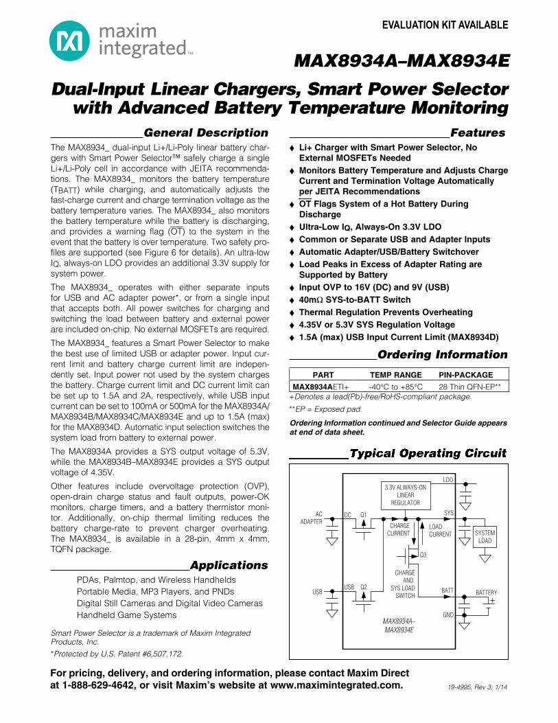
General DescriptionThe MAX8934_ dual-input Li+/Li-Poly linear battery char-gers with Smart Power SelectorK safely charge a single Li+/Li-Poly cell in accordance with JEITA recommenda-tions. The MAX8934_ monitors the battery temperature (TBATT) while charging, and automatically adjusts the fast-charge current and charge termination voltage as the battery temperature varies. The MAX8934_ also monitors the battery temperature while the battery is discharging, and provides a warning flag (OT) to the system in the event that the battery is over temperature. Two safety pro-files are supported (see Figure 6 for details). An ultra-low IQ, always-on LDO provides an additional 3.3V supply for system power.
The MAX8934_ operates with either separate inputs for USB and AC adapter power*, or from a single input that accepts both. All power switches for charging and switching the load between battery and external power are included on-chip. No external MOSFETs are required.
The MAX8934_ features a Smart Power Selector to make the best use of limited USB or adapter power. Input cur-rent limit and battery charge current limit are indepen-dently set. Input power not used by the system charges the battery. Charge current limit and DC current limit can be set up to 1.5A and 2A, respectively, while USB input current can be set to 100mA or 500mA for the MAX8934A/MAX8934B/MAX8934C/MAX8934E and up to 1.5A (max) for the MAX8934D. Automatic input selection switches the system load from battery to external power.
The MAX8934A provides a SYS output voltage of 5.3V, while the MAX8934B–MAX8934E provides a SYS output voltage of 4.35V.
Other features include overvoltage protection (OVP), open-drain charge status and fault outputs, power-OK monitors, charge timers, and a battery thermistor moni-tor. Additionally, on-chip thermal limiting reduces the battery charge-rate to prevent charger overheating. The MAX8934_ is available in a 28-pin, 4mm x 4mm, TQFN package.
ApplicationsPDAs, Palmtop, and Wireless HandheldsPortable Media, MP3 Players, and PNDsDigital Still Cameras and Digital Video CamerasHandheld Game Systems
FeaturesS Li+ Charger with Smart Power Selector, No
External MOSFETs Needed
S Monitors Battery Temperature and Adjusts Charge Current and Termination Voltage Automatically per JEITA Recommendations
S OT Flags System of a Hot Battery During Discharge
S Ultra-Low IQ, Always-On 3.3V LDO
S Common or Separate USB and Adapter Inputs
S Automatic Adapter/USB/Battery Switchover
S Load Peaks in Excess of Adapter Rating are Supported by Battery
S Input OVP to 16V (DC) and 9V (USB)
S 40mI SYS-to-BATT Switch
S Thermal Regulation Prevents Overheating
S 4.35V or 5.3V SYS Regulation Voltage
S 1.5A (max) USB Input Current Limit (MAX8934D)
Typical Operating Circuit
+Denotes a lead(Pb)-free/RoHS-compliant package.
**EP = Exposed pad.
Ordering Information continued and Selector Guide appears at end of data sheet.
Smart Power Selector is a trademark of Maxim Integrated Products, Inc.
*Protected by U.S. Patent #6,507,172.
Ordering Information
19-4995; Rev 3; 1/14
PART TEMP RANGE PIN-PACKAGE
MAX8934AETI+ -40NC to +85NC 28 Thin QFN-EP**
MAX8934A−MAX8934E
SYS
LDO
GND
CHARGECURRENT
LOADCURRENT
BATT BATTERY
SYSTEMLOAD
ACADAPTER
CHARGEAND
SYS LOADSWITCH
USB
DC Q1
Q2
Q3
USB
3.3V ALWAYS-ONLINEAR
REGULATOR
For pricing, delivery, and ordering information, please contact Maxim Direct at 1-888-629-4642, or visit Maxim’s website at www.maximintegrated.com.
2 Maxim Integrated
Dual-Input Linear Chargers, Smart Power Selector with Advanced Battery Temperature Monitoring
MAX8934A–MAX8934E
Stresses beyond those listed under “Absolute Maximum Ratings” may cause permanent damage to the device. These are stress ratings only, and functional operation of the device at these or any other conditions beyond those indicated in the operational sections of the specifications is not implied. Exposure to absolute maximum rating conditions for extended periods may affect device reliability.
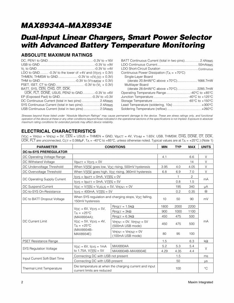
DC, PEN1 to GND .................................................-0.3V to +16VUSB to GND ............................................................-0.3V to +9VVL to GND ...............................................................-0.3V to +4VLDO to GND ......... -0.3V to the lower of +4V and (VSYS + 0.3V)THMEN, THMSW to GND ..................... -0.3V to +(VLDO + 0.3V)THM to GND .......................................-0.3V to (VTHMSW + 0.3V)PSET, ISET, CT to GND ............................... -0.3V to (VL + 0.3V)BATT, SYS, CEN, CHG, OT, DOK,
UOK, FLT, DONE, USUS, PEN2 to GND .............-0.3V to +6VEP (Exposed Pad) to GND ...................................-0.3V to +0.3VDC Continuous Current (total in two pins) ....................2.4ARMSSYS Continuous Current (total in two pins) ...................2.4ARMSUSB Continuous Current (total in two pins) ..................2.0ARMS
BATT Continuous Current (total in two pins) .................2.4ARMSLDO Continuous Current .............................................50mARMSLDO Short-Circuit Duration .........................................ContinuousContinuous Power Dissipation (TA = +70NC)
Single-Layer Board (derate 20.8mW/NC above +70NC) ......................1666.7mW Multilayer Board (derate 28.6mW/NC above +70NC) ......................2285.7mW
Operating Temperature Range .......................... -40NC to +85NCJunction Temperature ...................................... -40NC to +125NCStorage Temperature ....................................... -65NC to +150NCLead Temperature (soldering, 10s) ................................+300NCSoldering Temperature (reflow) ......................................+260NC
ELECTRICAL CHARACTERISTICS(VDC = VPEN1 = VPEN2 = 5V, CEN = USUS = THMEN = GND, VBATT = 4V, VTHM = 1.65V, USB, THMSW, CHG, DONE, OT, DOK, UOK, FLT are unconnected, CCT = 0.068FF, TA = -40NC to +85NC, unless otherwise noted. Typical values are at TA = +25NC.) (Note 1)
ABSOLUTE MAXIMUM RATINGS
PARAMETER CONDITIONS MIN TYP MAX UNITS
DC-to-SYS PREREGULATOR
DC Operating Voltage Range 4.1 6.6 V
DC Withstand Voltage VBATT = VSYS = 0V 14 V
DC Undervoltage Threshold When V DOK goes low, VDC rising, 500mV hysteresis 3.95 4.0 4.05 V
DC Overvoltage Threshold When V DOK goes high, VDC rising, 360mV hysteresis 6.8 6.9 7.0 V
DC Operating Supply CurrentISYS = IBATT = 0mA, V CEN = 0V 1 2
mAISYS = IBATT = 0mA, V CEN = 5V 0.8 1.5
DC Suspend Current VDC = V CEN = VUSUS = 5V, VPEN1 = 0V 195 340 FA
DC-to-SYS On-Resistance ISYS = 400mA, V CEN = 5V 0.2 0.35 I
DC to BATT Dropout VoltageWhen SYS regulation and charging stops, VDC falling, 150mV hysteresis
10 50 90 mV
DC Current Limit
VDC = 6V, VSYS = 5V, TA = +25NC (MAX8934A);VDC = 5V, VSYS = 4V, TA = +25NC (MAX8934B–MAX8934E)
RPSET = 1.5kI 1800 2000 2200
mA
RPSET = 3kI 900 1000 1100
RPSET = 6.3kI 450 475 500
VPEN1 = 0V, VPEN2 = 5V (500mA USB mode)
450 475 500
VPEN1 = VPEN2 = 0V (100mA USB mode)
80 95 100
PSET Resistance Range 1.5 6.3 kI
SYS Regulation VoltageVDC = 6V, ISYS = 1mA to 1.75A, V CEN = 5V
MAX8934A 5.2 5.3 5.4V
MAX8934B–MAX8934E 4.29 4.35 4.4
Input Current Soft-Start TimeConnecting DC with USB not present 1.5 ms
Connecting DC with USB present 50 Fs
Thermal-Limit TemperatureDie temperature at when the charging current and input current limits are reduced
100 NC
3Maxim Integrated
Dual-Input Linear Chargers, Smart Power Selector with Advanced Battery Temperature Monitoring
MAX8934A–MAX8934E
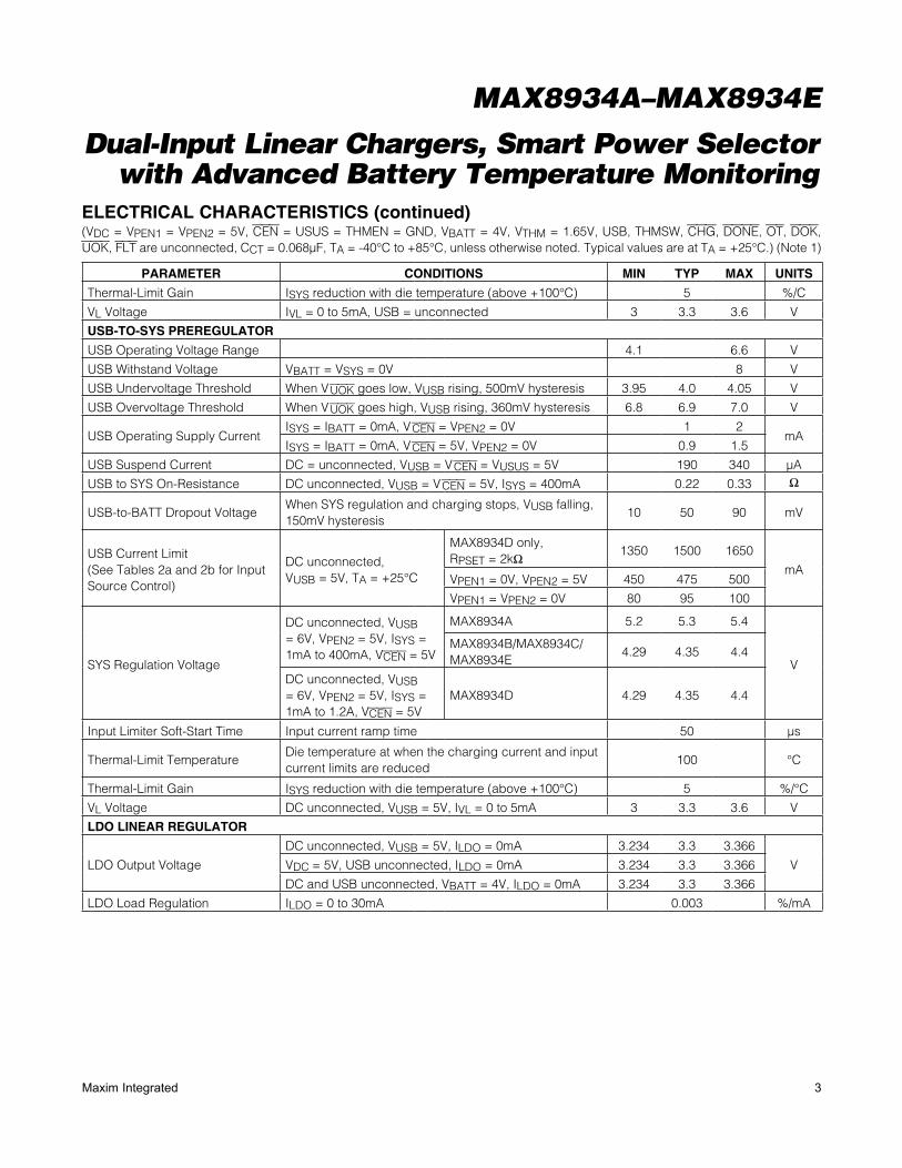
ELECTRICAL CHARACTERISTICS (continued)(VDC = VPEN1 = VPEN2 = 5V, CEN = USUS = THMEN = GND, VBATT = 4V, VTHM = 1.65V, USB, THMSW, CHG, DONE, OT, DOK, UOK, FLT are unconnected, CCT = 0.068FF, TA = -40NC to +85NC, unless otherwise noted. Typical values are at TA = +25NC.) (Note 1)
PARAMETER CONDITIONS MIN TYP MAX UNITS
Thermal-Limit Gain ISYS reduction with die temperature (above +100NC) 5 %/C
VL Voltage IVL = 0 to 5mA, USB = unconnected 3 3.3 3.6 V
USB-TO-SYS PREREGULATOR
USB Operating Voltage Range 4.1 6.6 V
USB Withstand Voltage VBATT = VSYS = 0V 8 V
USB Undervoltage Threshold When V UOK goes low, VUSB rising, 500mV hysteresis 3.95 4.0 4.05 V
USB Overvoltage Threshold When V UOK goes high, VUSB rising, 360mV hysteresis 6.8 6.9 7.0 V
USB Operating Supply CurrentISYS = IBATT = 0mA, V CEN = VPEN2 = 0V 1 2
mAISYS = IBATT = 0mA, V CEN = 5V, VPEN2 = 0V 0.9 1.5
USB Suspend Current DC = unconnected, VUSB = V CEN = VUSUS = 5V 190 340 FA
USB to SYS On-Resistance DC unconnected, VUSB = V CEN = 5V, ISYS = 400mA 0.22 0.33 I
USB-to-BATT Dropout VoltageWhen SYS regulation and charging stops, VUSB falling, 150mV hysteresis
10 50 90 mV
USB Current Limit(See Tables 2a and 2b for Input Source Control)
DC unconnected, VUSB = 5V, TA = +25NC
MAX8934D only, RPSET = 2kI
1350 1500 1650
mAVPEN1 = 0V, VPEN2 = 5V 450 475 500
VPEN1 = VPEN2 = 0V 80 95 100
SYS Regulation Voltage
DC unconnected, VUSB = 6V, VPEN2 = 5V, ISYS = 1mA to 400mA, VCEN = 5V
MAX8934A 5.2 5.3 5.4
V
MAX8934B/MAX8934C/ MAX8934E
4.29 4.35 4.4
DC unconnected, VUSB = 6V, VPEN2 = 5V, ISYS = 1mA to 1.2A, VCEN = 5V
MAX8934D 4.29 4.35 4.4
Input Limiter Soft-Start Time Input current ramp time 50 Fs
Thermal-Limit TemperatureDie temperature at when the charging current and input current limits are reduced
100 NC
Thermal-Limit Gain ISYS reduction with die temperature (above +100NC) 5 %/NC
VL Voltage DC unconnected, VUSB = 5V, IVL = 0 to 5mA 3 3.3 3.6 V
LDO LINEAR REGULATOR
LDO Output Voltage
DC unconnected, VUSB = 5V, ILDO = 0mA 3.234 3.3 3.366
VVDC = 5V, USB unconnected, ILDO = 0mA 3.234 3.3 3.366
DC and USB unconnected, VBATT = 4V, ILDO = 0mA 3.234 3.3 3.366
LDO Load Regulation ILDO = 0 to 30mA 0.003 %/mA
4 Maxim Integrated
Dual-Input Linear Chargers, Smart Power Selector with Advanced Battery Temperature Monitoring
MAX8934A–MAX8934E
ELECTRICAL CHARACTERISTICS (continued)(VDC = VPEN1 = VPEN2 = 5V, CEN = USUS = THMEN = GND, VBATT = 4V, VTHM = 1.65V, USB, THMSW, CHG, DONE, OT, DOK, UOK, FLT are unconnected, CCT = 0.068FF, TA = -40NC to +85NC, unless otherwise noted. Typical values are at TA = +25NC.) (Note 1)
PARAMETER CONDITIONS MIN TYP MAX UNITS
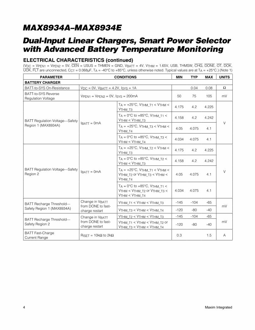
BATTERY CHARGER
BATT-to-SYS On-Resistance VDC = 0V, VBATT = 4.2V, ISYS = 1A 0.04 0.08 I
BATT-to-SYS ReverseRegulation Voltage
VPEN1 = VPEN2 = 0V, ISYS = 200mA 50 75 105 mV
BATT Regulation Voltage—Safety Region 1 (MAX8934A)
IBATT = 0mA
TA = +25NC, VTHM_T1 < VTHM < VTHM_T3
4.175 4.2 4.225
V
TA = 0NC to +85NC, VTHM_T1 < VTHM < VTHM_T3
4.158 4.2 4.242
TA = +25NC, VTHM_T3 < VTHM < VTHM_T4
4.05 4.075 4.1
TA = 0NC to +85NC, VTHM_T3 < VTHM < VTHM_T4
4.034 4.075 4.1
BATT Regulation Voltage—Safety Region 2
IBATT = 0mA
TA = +25NC, VTHM_T2 < VTHM < VTHM_T3
4.175 4.2 4.225
V
TA = 0NC to +85NC, VTHM_T2 < VTHM < VTHM_T3
4.158 4.2 4.242
TA = +25NC, VTHM_T1 < VTHM < VTHM_T2 or VTHM_T3 < VTHM < VTHM_T4
4.05 4.075 4.1
TA = 0NC to +85NC, VTHM_T1 < VTHM < VTHM_T2 or VTHM_T3 < VTHM < VTHM_T4
4.034 4.075 4.1
BATT Recharge Threshold—Safety Region 1 (MAX8934A)
Change in VBATT from DONE to fast-charge restart
VTHM_T1 < VTHM < VTHM_T3 -145 -104 -65mV
VTHM_T3 < VTHM < VTHM_T4 -120 -80 -40
BATT Recharge Threshold—Safety Region 2
Change in VBATT from DONE to fast-charge restart
VTHM_T2 < VTHM < VTHM_T3 -145 -104 -65
mVVTHM_T1 < VTHM < VTHM_T2 or VTHM_T3 < VTHM < VTHM_T4
-120 -80 -40
BATT Fast-ChargeCurrent Range
RISET = 10kI to 2kI 0.3 1.5 A
5Maxim Integrated
Dual-Input Linear Chargers, Smart Power Selector with Advanced Battery Temperature Monitoring
MAX8934A–MAX8934E
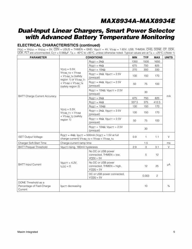
ELECTRICAL CHARACTERISTICS (continued)(VDC = VPEN1 = VPEN2 = 5V, CEN = USUS = THMEN = GND, VBATT = 4V, VTHM = 1.65V, USB, THMSW, CHG, DONE, OT, DOK, UOK, FLT are unconnected, CCT = 0.068FF, TA = -40NC to +85NC, unless otherwise noted. Typical values are at TA = +25NC.) (Note 1)
PARAMETER CONDITIONS MIN TYP MAX UNITS
BATT Charge Current Accuracy
VSYS = 5.5V, VTHM_T2 < VTHM < VTHM_T4 (safety region 1) or VTHM_T1 < VTHM < VTHM_T4 (safety region 2)
RISET = 2kI 1350 1500 1650
mA
RISET = 4kI 675 750 825
RISET = 10kI 270 300 330
RISET = 2kI, VBATT = 2.5V (prequal)
130 150 170
RISET = 4kI, VBATT = 2.5V (prequal)
50 75 100
RISET = 10kI, VBATT = 2.5V (prequal)
30
VSYS = 5.5V, VTHM_T1 < VTHM < VTHM_T2 (safety region 1)
RISET = 2kI 675 750 825
RISET = 4kI 337.5 375 412.5
RISET = 10kI 130 150 170
RISET = 2kI, VBATT = 2.5V (prequal)
130 150 170
RISET = 4kI, VBATT = 2.5V (prequal)
50 75 100
RISET = 10kI, VBATT = 2.5V (prequal)
30
ISET Output VoltageRISET = 4kI, IBATT = 500mA (VISET = 1.5V at full charge current) VTHM_T2 < VTHM < VTHM_T4
0.9 1 1.1 V
Charger Soft-Start Time Charge-current ramp time 1.5 ms
BATT Prequal Threshold VBATT rising, 180mV hysteresis 2.9 3 3.1 V
BATT Input CurrentVBATT = 4.2V, ILDO = 0
No DC or USB power connected, THMEN = low, VCEN = 5V
5 12
FANo DC or USB power connected, THMEN = high,V CEN = 5V
12 25
DC or USB power connected, V CEN = 5V
0.003 2
DONE Threshold as a Percentage of Fast-Charge Current
IBATT decreasing 10 %
6 Maxim Integrated
Dual-Input Linear Chargers, Smart Power Selector with Advanced Battery Temperature Monitoring
MAX8934A–MAX8934E
ELECTRICAL CHARACTERISTICS (continued)(VDC = VPEN1 = VPEN2 = 5V, CEN = USUS = THMEN = GND, VBATT = 4V, VTHM = 1.65V, USB, THMSW, CHG, DONE, OT, DOK, UOK, FLT are unconnected, CCT = 0.068FF, TA = -40NC to +85NC, unless otherwise noted. Typical values are at TA = +25NC.) (Note 1)
PARAMETER CONDITIONS MIN TYP MAX UNITS
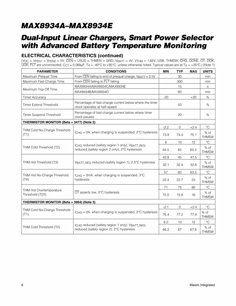
Maximum Prequal Time From CEN falling to end of prequal charge, VBATT = 2.5V 30 min
Maximum Fast-Charge Time From CEN falling to FLT falling 300 min
Maximum Top-Off TimeMAX8934A/MAX8934C/MAX8934E 15 s
MAX8934B/MAX8934D 60 min
Timer Accuracy -20 +20 %
Timer Extend ThresholdPercentage of fast-charge current below where the timer clock operates at half-speed
50 %
Timer Suspend ThresholdPercentage of fast-charge current below where timer clock pauses
20 %
THERMISTOR MONITOR (Beta = 3477) (Note 2)
THM Cold No-Charge Threshold (T1)
ICHG = 0A, when charging is suspended, 2NC hysteresis
-2.2 0 +2.4 NC
73.9 74.4 75.1% of
THMSW
THM Cold Threshold (T2)ICHG reduced (safety region 1 only), VBATT_REG reduced (safety region 2 only), 2NC hysteresis
8 10 12 NC
64.5 65 65.5% of
THMSW
THM Hot Threshold (T3) VBATT_REG reduced (safety region 1), 2.5NC hysteresis
42.8 45 47.5 NC
32.1 32.4 32.8% of
THMSW
THM Hot No-Charge Threshold (T4)
ICHG = 0mA, when charging is suspended, 3NC hysteresis
57 60 63.5 NC
22.4 22.7 23% of
THMSW
THM Hot Overtemperature Threshold (TOT)
OT asserts low, 5NC hysteresis
71 75 80 NC
15.5 15.8 16% of
THMSW
THERMISTOR MONITOR (Beta = 3964) (Note 3)
THM Cold No-Charge Threshold (T1)
ICHG = 0A, when charging is suspended, 2NC hysteresis
-2.1 0 +2.4 NC
76.4 77.2 77.9% of THMSW
THM Cold Threshold (T2)ICHG reduced (safety region 1 only), VBATT_REG reduced (safety region 2), 2NC hysteresis
8.2 10 12 NC
66.2 67 67.6% of
THMSW
7Maxim Integrated
Dual-Input Linear Chargers, Smart Power Selector with Advanced Battery Temperature Monitoring
MAX8934A–MAX8934E
ELECTRICAL CHARACTERISTICS (continued)(VDC = VPEN1 = VPEN2 = 5V, CEN = USUS = THMEN = GND, VBATT = 4V, VTHM = 1.65V, USB, THMSW, CHG, DONE, OT, DOK, UOK, FLT are unconnected, CCT = 0.068FF, TA = -40NC to +85NC, unless otherwise noted. Typical values are at TA = +25NC.) (Note 1)
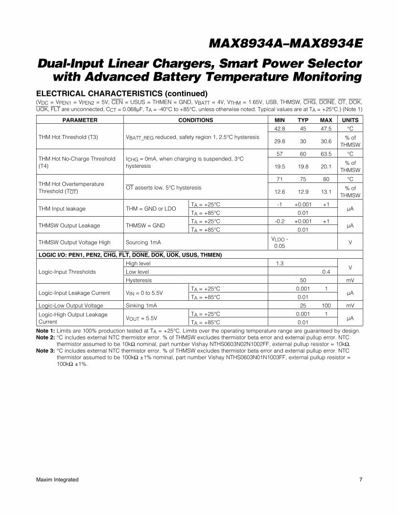
Note 1: Limits are 100% production tested at TA = +25NC. Limits over the operating temperature range are guaranteed by design.Note 2: NC includes external NTC thermistor error. % of THMSW excludes thermistor beta error and external pullup error. NTC
thermistor assumed to be 10kI nominal, part number Vishay NTHS0603N02N1002FF, external pullup resistor = 10kI. Note 3: NC includes external NTC thermistor error. % of THMSW excludes thermistor beta error and external pullup error. NTC
thermistor assumed to be 100kI Q1% nominal, part number Vishay NTHS0603N01N1003FF, external pullup resistor = 100kI Q1%.
PARAMETER CONDITIONS MIN TYP MAX UNITS
THM Hot Threshold (T3) VBATT_REG reduced, safety region 1, 2.5NC hysteresis
42.8 45 47.5 NC
29.8 30 30.6% of
THMSW
THM Hot No-Charge Threshold (T4)
ICHG = 0mA, when charging is suspended, 3NC hysteresis
57 60 63.5 NC
19.5 19.8 20.1% of
THMSW
THM Hot Overtemperature Threshold (TOT)
OT asserts low, 5NC hysteresis
71 75 80 NC
12.6 12.9 13.1% of
THMSW
THM Input leakage THM = GND or LDOTA = +25NC -1 +0.001 +1
FATA = +85NC 0.01
THMSW Output Leakage THMSW = GNDTA = +25NC -0.2 +0.001 +1
FATA = +85NC 0.01
THMSW Output Voltage High Sourcing 1mAVLDO - 0.05
V
LOGIC I/O: PEN1, PEN2, CHG, FLT, DONE, DOK, UOK, USUS, THMEN)
Logic-Input Thresholds
High level 1.3V
Low level 0.4
Hysteresis 50 mV
Logic-Input Leakage Current VIN = 0 to 5.5VTA = +25NC 0.001 1
FATA = +85NC 0.01
Logic-Low Output Voltage Sinking 1mA 25 100 mV
Logic-High Output Leakage Current
VOUT = 5.5VTA = +25NC 0.001 1
FATA = +85NC 0.01
8 Maxim Integrated
Dual-Input Linear Chargers, Smart Power Selector with Advanced Battery Temperature Monitoring
MAX8934A–MAX8934E
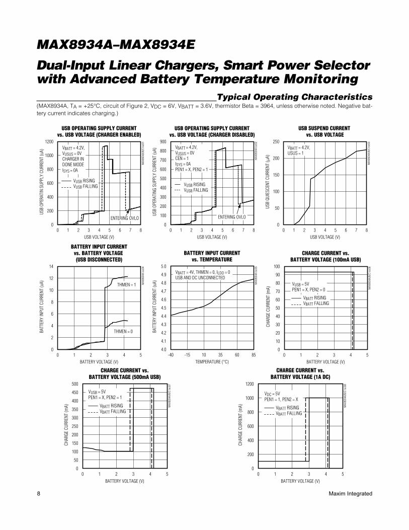
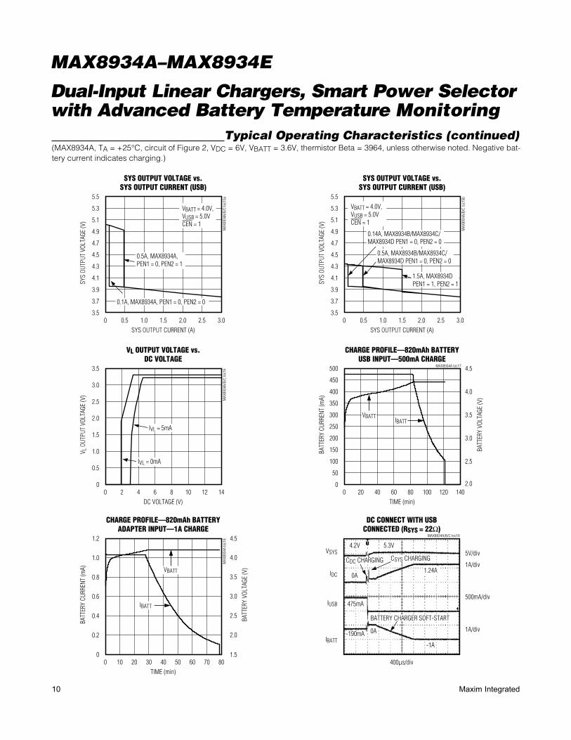
Typical Operating Characteristics(MAX8934A, TA = +25NC, circuit of Figure 2, VDC = 6V, VBATT = 3.6V, thermistor Beta = 3964, unless otherwise noted. Negative bat-tery current indicates charging.)
USB OPERATING SUPPLY CURRENTvs. USB VOLTAGE (CHARGER ENABLED)
MAX
8934
A/B/
C to
c01
USB
OPER
ATIN
SUP
PLY
CURR
ENT
(uA)
200
400
600
800
1000
1200
0
USB VOLTAGE (V)
764 52 310 8
VBATT = 4.2V,VUSUS = 0VCHARGER INDONE MODEISYS = 0A
VUSB RISINGVUSB FALLING
ENTERING OVLO
USB OPERATING SUPPLY CURRENTvs. USB VOLTAGE (CHARGER DISABLED)
MAX
8934
A to
c02
USB VOLTAGE (V)
USB
OPER
ATIN
G SU
PPLY
CUR
RENT
(uA)
764 52 31
100
200
300
400
500
600
700
800
900
00 8
VBATT = 4.2V,VUSUS = 0VCEN = 1ISYS = 0APEN1 = X, PEN2 = 1
VUSB RISINGVUSB FALLING
ENTERING OVLO
USB SUSPEND CURRENT vs. USB VOLTAGE
MAX
8934
A/B/
C to
c03
USB VOLTAGE (V)
USB
QUIE
SCEN
T CU
RREN
T (F
A)
7654321
50
100
150
200
250
00 8
VBATT = 4.2V,USUS = 1
BATTERY INPUT CURRENTvs. BATTERY VOLTAGE (USB DISCONNECTED)
MAX
8934
A to
c04
BATTERY VOLTAGE (V)
BATT
ERY
INPU
T CU
RREN
T (u
A)
4321
2
4
6
8
10
12
14
00 5
THMEN = 1
THMEN = 0
CHARGE CURRENT vs.BATTERY VOLTAGE (500mA USB)
MAX
8934
A/B/
C to
c07
BATTERY VOLTAGE (V)
CHAR
GE C
URRE
NT (m
A)
4321
50
100
150
200
250
300
350
400
450
500
00 5
VUSB = 5VPEN1 = X, PEN2 = 1
VBATT RISINGVBATT FALLING
CHARGE CURRENT vs.BATTERY VOLTAGE (1A DC)
MAX
8934
A/B/
C to
c08
BATTERY VOLTAGE (V)
CHAR
GE C
URRE
NT (m
A)
4321
200
400
600
800
1000
1200
00 5
VDC = 5VPEN1 = 1, PEN2 = X
VBATT RISINGVBATT FALLING
BATTERY INPUT CURRENTvs. TEMPERATURE
MAX
8934
A to
c05
TEMPERATURE (°C)
BATT
ERY
INPU
T CU
RREN
T (u
A)
603510-15
4.1
4.2
4.3
4.4
4.5
4.6
4.7
4.8
4.9
5.0
4.0-40 85
VBATT = 4V, THMEN = 0, ILDO = 0USB AND DC UNCONNECTED
CHARGE CURRENT vs.BATTERY VOLTAGE (100mA USB)
MAX
8934
A/B/
C to
c06
BATTERY VOLTAGE (V)
CHAR
GE C
URRE
NT (m
A)
4321
10
20
30
40
50
60
70
80
90
100
00 5
VUSB = 5VPEN1 = X, PEN2 = 0
VBATT RISINGVBATT FALLING
9Maxim Integrated
Dual-Input Linear Chargers, Smart Power Selector with Advanced Battery Temperature Monitoring
MAX8934A–MAX8934E
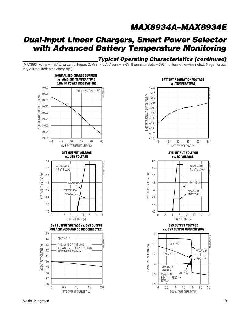
Typical Operating Characteristics (continued)(MAX8934A, TA = +25NC, circuit of Figure 2, VDC = 6V, VBATT = 3.6V, thermistor Beta = 3964, unless otherwise noted. Negative bat-tery current indicates charging.)
BATTERY REGULATION VOLTAGEvs. TEMPERATURE
MAX
8934
A to
c10
BATTERY VOLTAGE (V)BA
TTER
Y RE
GULA
TION
VOL
TAGE
(V)
603510-15
4.175
4.180
4.185
4.190
4.195
4.200
4.205
4.210
4.215
4.220
4.170-40 85
SYS OUTPUT VOLTAGEvs. DC VOLTAGE
MAX
8934
A/B/
C to
c12
DC VOLTAGE (V)
SYS
OUTP
UT V
OLTA
GE (V
)
12108642
4.2
4.4
4.6
4.8
5.0
5.2
5.4
4.00 14
VBATT = 4.0VNO SYS LOAD
MAX8934A
MAX8934B–MAX8934E
SYS OUTPUT VOLTAGEvs. SYS OUTPUT CURRENT (DC)
MAX
8934
A/B/
C to
c14
SYS OUTPUT CURRENT (A)
SYS
OUTP
UT V
OLTA
GE (V
)
2.52.01.51.00.5
3.9
4.3
4.7
5.1
5.5
3.50 3.0
VDC = 6V
VBATT = 4V,PEN1 = 1, PEN2 = XCEN = 1
MAX8934A
MAX8934B–MAX8934E
VDC = 6V
VDC = 5V
VDC = 5V
NORMALIZED CHARGE CURRENTvs. AMBIENT TEMPERATURE(LOW IC POWER DISSIPATION)
MAX
1960
toc0
9
AMBIENT TEMPERATURE (°C)
NORM
ALIZ
ED C
HARG
E CU
RREN
T
6035-15 10
0.9925
0.9950
0.9975
1.0000
1.0050
1.0025
1.0075
1.0100
0.9900-40 85
VUSB = 5V, VBATT = 4V
SYS OUTPUT VOLTAGEvs. USB VOLTAGE
MAX
8934
A/B/
C to
c11
USB VOLTAGE (V)
SYS
OUTP
UT V
OLTA
GE (V
)
7654321
4.2
4.4
4.6
4.8
5.0
5.2
5.4
4.00 8
VBATT = 4.0VNO SYS LOAD
MAX8934A
MAX8934B–MAX8934E
SYS OUTPUT VOLTAGE vs. SYS OUTPUTCURRENT (USB AND DC DISCONNECTED)
MAX
8934
A/B/
C to
c13
SYS OUTPUT CURRENT (A)
SYS
OUTP
UT V
OLTA
GE (V
)
1.51.00.5
3.7
3.8
3.9
4.0
4.1
4.2
4.3
4.4
4.5
3.60 2.0
VBATT = 4.0V
THE SLOPE OF THIS LINESHOWS THAT THE BATT-TO-SYSRESISTANCE IS 40mI.
10 Maxim Integrated
Dual-Input Linear Chargers, Smart Power Selector with Advanced Battery Temperature Monitoring
MAX8934A–MAX8934E
Typical Operating Characteristics (continued)(MAX8934A, TA = +25NC, circuit of Figure 2, VDC = 6V, VBATT = 3.6V, thermistor Beta = 3964, unless otherwise noted. Negative bat-tery current indicates charging.)
SYS OUTPUT VOLTAGE vs.SYS OUTPUT CURRENT (USB)
MAX
8934
A/B/
C to
c15b
SYS OUTPUT CURRENT (A)SY
S OU
TPUT
VOL
TAGE
(V)
2.52.01.51.00.5
3.7
3.9
4.1
4.3
4.5
4.7
4.9
5.1
5.3
5.5
3.50 3.0
VBATT = 4.0V,VUSB = 5.0VCEN = 1
0.14A, MAX8934B/MAX8934C/MAX8934D PEN1 = 0, PEN2 = 0
0.5A, MAX8934B/MAX8934C/MAX8934D PEN1 = 0, PEN2 = 0
1.5A, MAX8934DPEN1 = 1, PEN2 = 1
CHARGE PROFILE—820mAh BATTERYUSB INPUT—500mA CHARGE
MAX8934A toc17
TIME (min)
BATT
ERY
CURR
ENT
(mA)
12010060 804020
50
100
150
200
250
300
350
VBATTIBATT
400
450
500
0BA
TTER
Y VO
LTAG
E (V
)
2.5
3.0
3.5
4.0
4.5
2.00 140
DC CONNECT WITH USBCONNECTED (RSYS = 22I)
MAX8934A/B/C toc19
500mA/div
5V/div
1A/div
1A/div
IBATT
IUSB
IDC
VSYS
400Fs/div
4.2V 5.3V
0A
0A
475mA
-190mA
CDC CHARGING CSYS CHARGING
-1A
1.24A
BATTERY CHARGER SOFT-START
SYS OUTPUT VOLTAGE vs.SYS OUTPUT CURRENT (USB)
MAX
8934
A/B/
C to
c15a
SYS OUTPUT CURRENT (A)
SYS
OUTP
UT V
OLTA
GE (V
)
2.52.01.51.00.5
3.7
3.9
4.1
4.3
4.5
4.7
4.9
5.1
5.3
5.5
3.50 3.0
VBATT = 4.0V,VUSB = 5.0VCEN = 1
0.5A, MAX8934A,PEN1 = 0, PEN2 = 1
0.1A, MAX8934A, PEN1 = 0, PEN2 = 0
VL OUTPUT VOLTAGE vs.DC VOLTAGE
MAX
8934
A/B/
C to
c16
DC VOLTAGE (V)
V L O
UTPU
T VO
LTAG
E (V
)
12108642
0.5
1.0
1.5
2.0
2.5
3.0
3.5
00 14
IVL = 5mA
IVL = 0mA
CHARGE PROFILE—820mAh BATTERYADAPTER INPUT—1A CHARGE
MAX
8934
A to
c18
TIME (min)
BATT
ERY
CURR
ENT
(mA)
70605040302010
0.2
0.4
0.6IBATT
VBATT0.8
1.0
1.2
0
BATT
ERY
VOLT
AGE
(V)
2.0
2.5
3.5
3.0
4.0
4.5
1.50 80
11Maxim Integrated
Dual-Input Linear Chargers, Smart Power Selector with Advanced Battery Temperature Monitoring
MAX8934A–MAX8934E
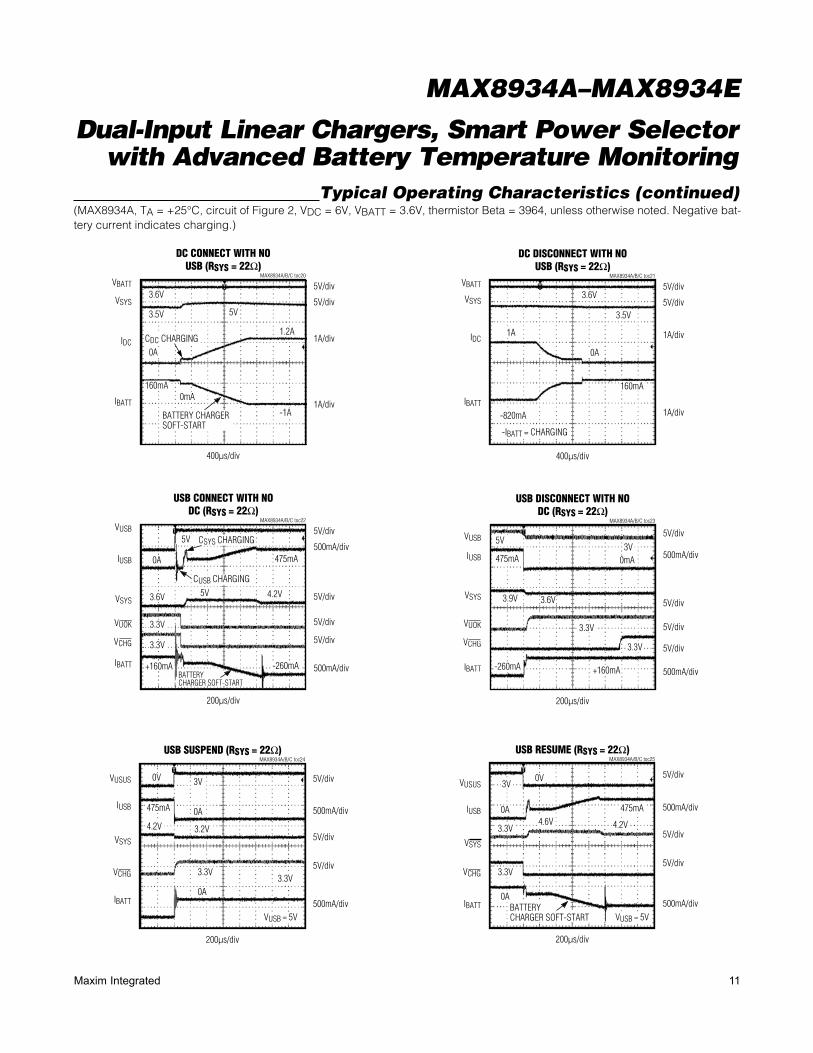
Typical Operating Characteristics (continued)(MAX8934A, TA = +25NC, circuit of Figure 2, VDC = 6V, VBATT = 3.6V, thermistor Beta = 3964, unless otherwise noted. Negative bat-tery current indicates charging.)
DC DISCONNECT WITH NOUSB (RSYS = 22I)
MAX8934A/B/C toc21
400Fs/div
3.6V
3.5V
0A
160mA
-820mA
-IBATT = CHARGING
1A
5V/div
1A/div
1A/div
5V/div
IBATT
IDC
VSYS
VBATT
USB DISCONNECT WITH NODC (RSYS = 22I)
MAX8934A/B/C toc23
200Fs/div
-260mA
3.9V
3.3V
3.3V
0mA3V
+160mA
3.6V
475mA
5V
500mA/div
5V/div
5V/div
5V/div
500mA/div
5V/div
IBATT
IUSB
VUSB
VCHG
VUOK
VSYS
USB RESUME (RSYS = 22I)MAX8934A/B/C toc25
200Fs/div
0V
4.6V 4.2V
475mA
3V
0A
0A
3.3V
3.3V
500mA/div
5V/div
5V/div
500mA/div
5V/div
IBATT
IUSB
VUSUS
VCHG
VSYS
BATTERYCHARGER SOFT-START VUSB = 5V
DC CONNECT WITH NOUSB (RSYS = 22I)
MAX8934A/B/C toc20
400Fs/div
3.6V
5V3.5V
0A
160mA0mA
1.2A
-1A
CDC CHARGING
5V/div
1A/div
1A/div
5V/div
IBATT
IDC
VSYS
VBATT
BATTERY CHARGERSOFT-START
USB CONNECT WITH NODC (RSYS = 22I)
MAX8934A/B/C toc22
200Fs/div
5V
5V
CSYS CHARGING
CUSB CHARGING
475mA
4.2V
0A
-260mA+160mA
3.3V
3.3V
3.6V
500mA/div
5V/div
5V/div
5V/div
500mA/div
5V/div
IBATT
IUSB
VUSB
VCHG
VUOK
VSYS
BATTERYCHARGER SOFT-START
USB SUSPEND (RSYS = 22I)MAX8934A/B/C toc24
200Fs/div
3V
VUSB = 5V
0A
3.2V
3.3V3.3V
0A
0V
475mA
4.2V
500mA/div
5V/div
5V/div
500mA/div
5V/div
IBATT
IUSB
VUSUS
VCHG
VSYS
12 Maxim Integrated
Dual-Input Linear Chargers, Smart Power Selector with Advanced Battery Temperature Monitoring
MAX8934A–MAX8934E
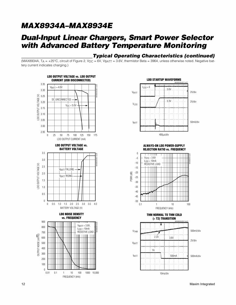
Typical Operating Characteristics (continued)(MAX8934A, TA = +25NC, circuit of Figure 2, VDC = 6V, VBATT = 3.6V, thermistor Beta = 3964, unless otherwise noted. Negative bat-tery current indicates charging.)
LDO OUTPUT VOLTAGE vs. LDO OUTPUTCURRENT (USB DISCONNECTED)
MAX
8934
A/B/
C to
c26
LDO OUTPUT CURRENT (mA)
LDO
OUTP
UT V
OLTA
GE (V
)
15012525 50 75 100
3.00
3.05
3.10
3.15
3.20
3.25
3.30
3.35
2.950 175
VDC = 5.0V
VBATT = 4.0V
DC UNCONNECTED
LDO OUTPUT VOLTAGE vs.BATTERY VOLTAGE
MAX
8934
A/B/
C to
c28
BATTERY VOLTAGE (V)
LDO
OUTP
UT V
OLTA
GE (V
)
3.53.02.52.01.51.00.5
0.5
1.0
1.5
2.0
2.5
3.0
3.5
00 4.0
VBATT RISING
VBATT FALLING
LDO NOISE DENSITYvs. FREQUENCY
MAX
8934
A to
c30
FREQUENCY (kHz)
OUTP
UT N
OISE
(nV/
Hz)
10001001010.1
100
200
300
400
500
600
700
800
900
00.01 10,000
VBATT = 3.8V, ILDO = 10mARESISTIVE LOAD
LDO STARTUP WAVEFORMSMAX8934A/B/C toc27
2V/div
50mA/div
2V/div
IBATT
VLDO
VBATT
400Fs/div
3.6VILDO = 0
3.3V
ALWAYS-ON LDO POWER-SUPPLY REJECTION RATIO vs. FREQUENCY
MAX
8934
A to
c29
FREQUENCY (kHz)
PSRR
(dB)
101
-45
-40
-35
-30
-25
-20
-15
-10
-5
0
-500.1 100
VSYS = 3.6VILDO = 10mARESISTIVE LOAD
THM NORMAL TO THM COLD(< T2) TRANSITION
MAX8934A/B/C toc31
2V/div
500mV/div
500mA/divIBATT
VBATT
VTHM
10ms/div
2.2V 3.6V
1A
500mA
13Maxim Integrated
Dual-Input Linear Chargers, Smart Power Selector with Advanced Battery Temperature Monitoring
MAX8934A–MAX8934E
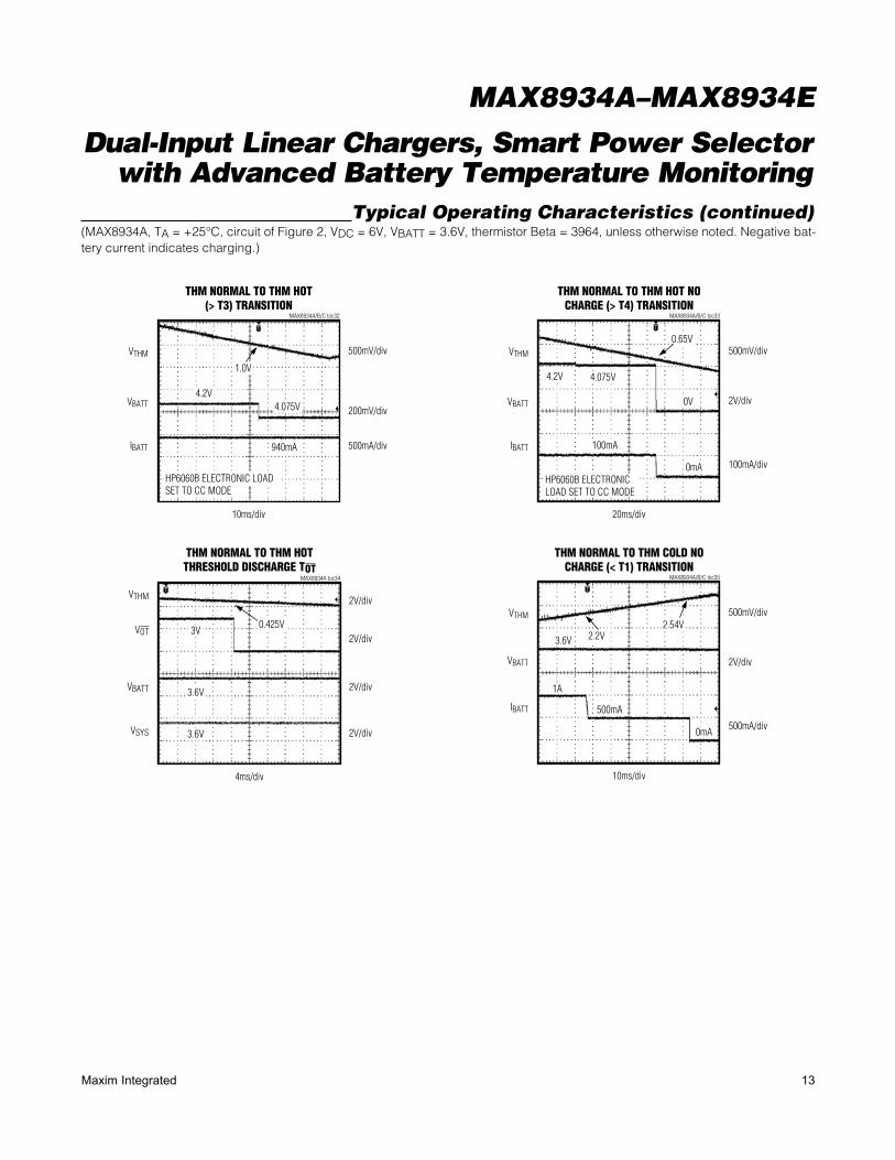
Typical Operating Characteristics (continued)(MAX8934A, TA = +25NC, circuit of Figure 2, VDC = 6V, VBATT = 3.6V, thermistor Beta = 3964, unless otherwise noted. Negative bat-tery current indicates charging.)
THM NORMAL TO THM HOT(> T3) TRANSITION
MAX8934A/B/C toc32
500mV/div
200mV/div
500mA/divIBATT
VBATT
VTHM
10ms/div
1.0V
4.2V
HP6060B ELECTRONIC LOADSET TO CC MODE
4.075V
940mA
MAX8934A toc34
2V/div
2V/div
2V/div
2V/div
VTHM
VBATT
VSYS
4ms/div
THM NORMAL TO THM HOTTHRESHOLD DISCHARGE TOT
VOT 3V
3.6V
3.6V
0.425V
THM NORMAL TO THM HOT NOCHARGE (> T4) TRANSITION
MAX8934A/B/C toc33
500mV/div
2V/div
100mA/div
IBATT
VBATT
VTHM
20ms/div
0.65V
4.2V
0V
0mA
100mA
4.075V
HP6060B ELECTRONIC LOAD SET TO CC MODE
THM NORMAL TO THM COLD NOCHARGE (< T1) TRANSITION
MAX8934A/B/C toc35
500mV/div
2V/div
500mA/div
IBATT
VBATT
VTHM
10ms/div
2.2V2.54V
3.6V
1A
500mA
0mA
14 Maxim Integrated
Dual-Input Linear Chargers, Smart Power Selector with Advanced Battery Temperature Monitoring
MAX8934A–MAX8934E
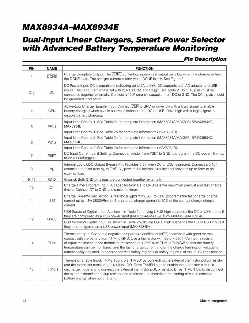
Pin Description
PIN NAME FUNCTION
1 DONECharge Complete Output. The DONE active-low, open-drain output pulls low when the charger enters the DONE state. The charger current = 0mA when DONE is low. See Figure 8.
2, 3 DC
DC Power Input. DC is capable of delivering up to 2A to SYS. DC supports both AC adapter and USB inputs. The DC current limit is set with PEN1, PEN2, and RPSET. See Table 2. Both DC pins must be connected together externally. Connect a 10FF ceramic capacitor from DC to GND. The DC inputs should be grounded if not used.
4 CENActive-Low Charger Enable Input. Connect CEN to GND or drive low with a logic signal to enable battery charging when a valid source is connected at DC or USB. Drive high with a logic signal to disable battery charging.
5 PEN1Input Limit Control 1. See Table 2a for complete information (MAX8934A/MAX8934B/MAX8934C/ MAX8934E).
Input Limit Control 1. See Table 2b for complete information (MAX8934D).
6 PEN2Input Limit Control 2. See Table 2a for complete information (MAX8934A/MAX8934B/MAX8934C/ MAX8934E).
Input Limit Control 2. See Table 2b for complete information (MAX8934D).
7 PSETDC Input Current-Limit Setting. Connect a resistor from PSET to GND to program the DC current limit up to 2A (3000/RPSET).
8 VL
Internal Logic LDO Output Bypass Pin. Provides 3.3V when DC or USB is present. Connect a 0.1FF ceramic capacitor from VL to GND. VL powers the internal circuitry and provides up to 5mA to an external load.
9, 13 GND Ground. Both GND pins must be connected together externally.
10 CTCharge Timer Program Input. A capacitor from CT to GND sets the maximum prequal and fast-charge timers. Connect CT to GND to disable the timer.
11 ISETCharge Current-Limit Setting. A resistor (RISET) from ISET to GND programs the fast-charge charge current up to 1.5A (3000/RISET). The prequal charge current is 10% of the set fast-charge charge current.
12 USUS
USB Suspend Digital Input. As shown in Table 2a, driving USUS high suspends the DC or USB inputs if they are configured as a USB power input (MAX8934A/MAX8934B/MAX8934C/MAX8934E).
USB Suspend Digital Input. As shown in Table 2b, driving USUS high suspends the DC or USB inputs if they are configured as a USB power input (MAX8934D).
14 THM
Thermistor Input. Connect a negative temperature coefficient (NTC) thermistor with good thermal contact with the battery from THM to GND. Use a thermistor with Beta = 3964. Connect a resistor of equal resistance to the thermistor resistance at +25°C from THM to THMSW so that the battery temperature can be monitored, and the fast-charge current and/or the charge termination voltage is automatically adjusted, in accordance with safety region 1 or safety region 2 of the JEITA specification.
15 THMEN
Thermistor Enable Input. THMEN controls THMSW by connecting the external thermistor pullup resistor and the thermistor monitoring circuit to LDO. Drive THMEN high to enable the thermistor circuit in discharge mode and to connect the external thermistor pullup resistor. Drive THMEN low to disconnect the external thermistor pullup resistor and to disable the thermistor monitoring circuit to conserve battery energy when not charging.
15Maxim Integrated
Dual-Input Linear Chargers, Smart Power Selector with Advanced Battery Temperature Monitoring
MAX8934A–MAX8934E
Pin Description (continued)
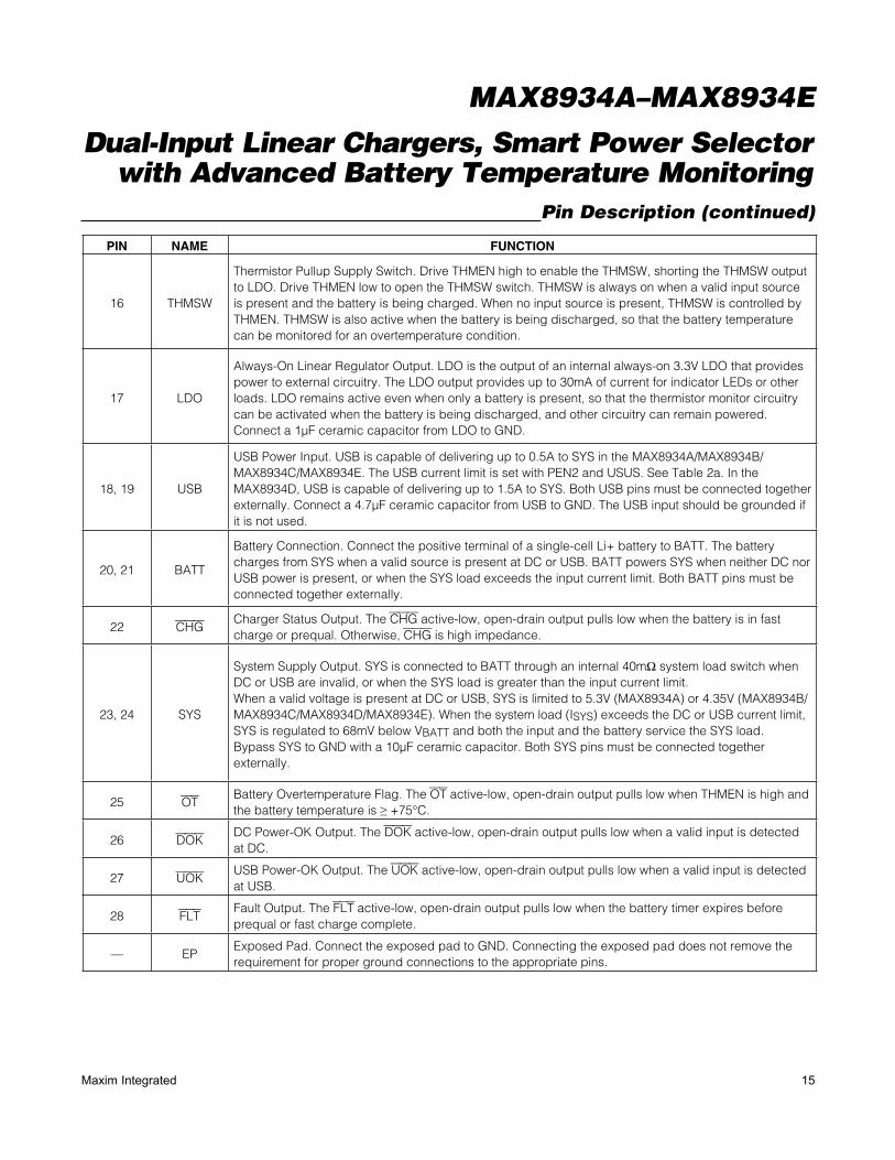
PIN NAME FUNCTION
16 THMSW
Thermistor Pullup Supply Switch. Drive THMEN high to enable the THMSW, shorting the THMSW output to LDO. Drive THMEN low to open the THMSW switch. THMSW is always on when a valid input source is present and the battery is being charged. When no input source is present, THMSW is controlled by THMEN. THMSW is also active when the battery is being discharged, so that the battery temperature can be monitored for an overtemperature condition.
17 LDO
Always-On Linear Regulator Output. LDO is the output of an internal always-on 3.3V LDO that provides power to external circuitry. The LDO output provides up to 30mA of current for indicator LEDs or other loads. LDO remains active even when only a battery is present, so that the thermistor monitor circuitry can be activated when the battery is being discharged, and other circuitry can remain powered. Connect a 1FF ceramic capacitor from LDO to GND.
18, 19 USB
USB Power Input. USB is capable of delivering up to 0.5A to SYS in the MAX8934A/MAX8934B/ MAX8934C/MAX8934E. The USB current limit is set with PEN2 and USUS. See Table 2a. In the MAX8934D, USB is capable of delivering up to 1.5A to SYS. Both USB pins must be connected together externally. Connect a 4.7FF ceramic capacitor from USB to GND. The USB input should be grounded if it is not used.
20, 21 BATT
Battery Connection. Connect the positive terminal of a single-cell Li+ battery to BATT. The battery charges from SYS when a valid source is present at DC or USB. BATT powers SYS when neither DC nor USB power is present, or when the SYS load exceeds the input current limit. Both BATT pins must be connected together externally.
22 CHGCharger Status Output. The CHG active-low, open-drain output pulls low when the battery is in fast charge or prequal. Otherwise, CHG is high impedance.
23, 24 SYS
System Supply Output. SYS is connected to BATT through an internal 40mI system load switch when DC or USB are invalid, or when the SYS load is greater than the input current limit.When a valid voltage is present at DC or USB, SYS is limited to 5.3V (MAX8934A) or 4.35V (MAX8934B/MAX8934C/MAX8934D/MAX8934E). When the system load (ISYS) exceeds the DC or USB current limit, SYS is regulated to 68mV below VBATT and both the input and the battery service the SYS load.Bypass SYS to GND with a 10FF ceramic capacitor. Both SYS pins must be connected together externally.
25 OTBattery Overtemperature Flag. The OT active-low, open-drain output pulls low when THMEN is high and the battery temperature is R +75NC.
26 DOKDC Power-OK Output. The DOK active-low, open-drain output pulls low when a valid input is detected at DC.
27 UOKUSB Power-OK Output. The UOK active-low, open-drain output pulls low when a valid input is detected at USB.
28 FLTFault Output. The FLT active-low, open-drain output pulls low when the battery timer expires before prequal or fast charge complete.
— EPExposed Pad. Connect the exposed pad to GND. Connecting the exposed pad does not remove the requirement for proper ground connections to the appropriate pins.
16 Maxim Integrated
Dual-Input Linear Chargers, Smart Power Selector with Advanced Battery Temperature Monitoring
MAX8934A–MAX8934E
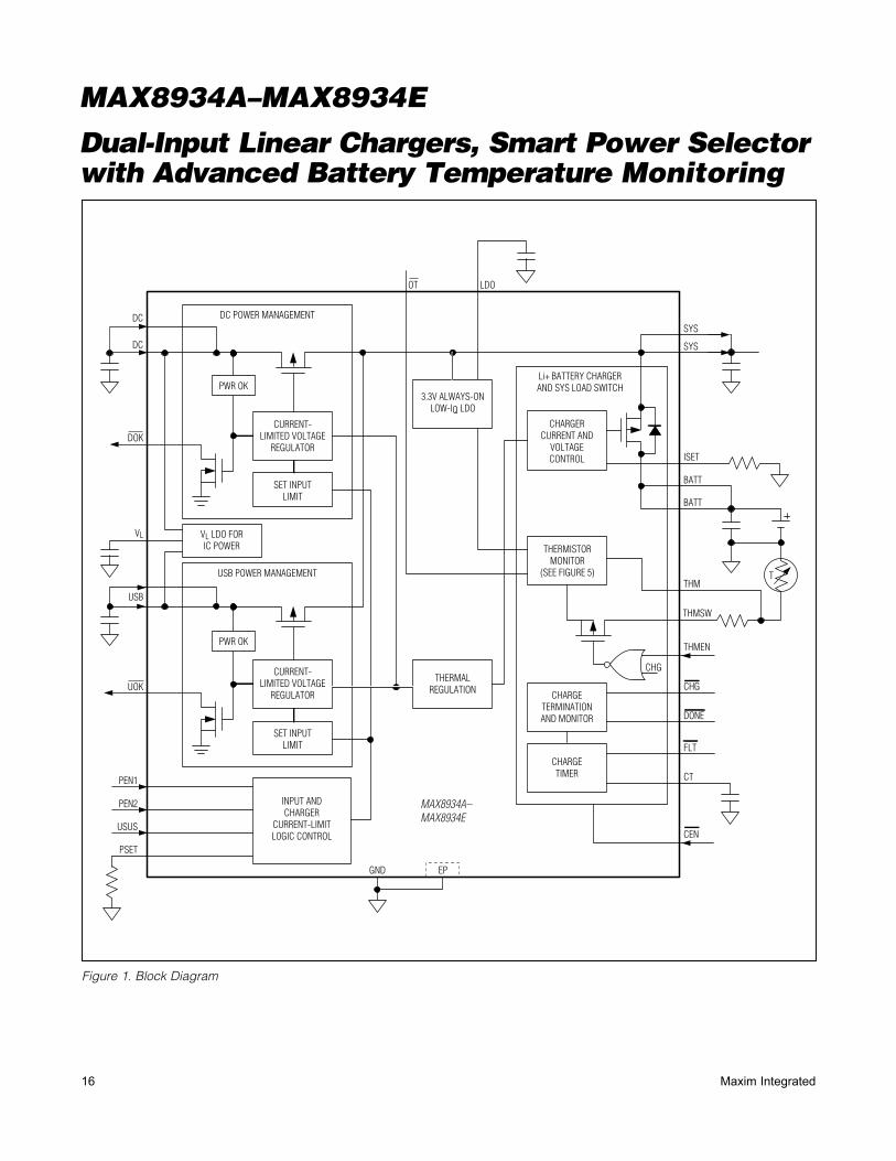
Figure 1. Block Diagram
SET INPUTLIMIT
VL LDO FORIC POWER
CURRENT-LIMITED VOLTAGE
REGULATOR
THERMISTORMONITOR
(SEE FIGURE 5)
CHARGETERMINATIONAND MONITOR
PWR OK
DC
DC
DOK
VL
USB
UOK
PEN1
PEN2
USUS
PSET
GND EP
DC POWER MANAGEMENT
Li+ BATTERY CHARGERAND SYS LOAD SWITCH
SYS
T
SYS
LDOOT
ISET
BATT
BATT
THM
THMSW
THMEN
CT
CHG
SET INPUTLIMIT
CURRENT-LIMITED VOLTAGE
REGULATOR
INPUT ANDCHARGER
CURRENT-LIMITLOGIC CONTROL
CHARGERCURRENT AND
VOLTAGECONTROL
THERMALREGULATION
PWR OK
USB POWER MANAGEMENT
3.3V ALWAYS-ONLOW-IQ LDO
CHARGETIMER
MAX8934A–MAX8934E
CEN
FLT
DONE
CHG
17Maxim Integrated
Dual-Input Linear Chargers, Smart Power Selector with Advanced Battery Temperature Monitoring
MAX8934A–MAX8934E
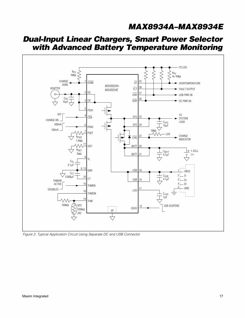
Figure 2. Typical Application Circuit Using Separate DC and USB Connector
DC
CHARGEDONE
ADAPTER
RPU1MI
RPU4x 1MI
CDC10FF
CSYS10FF
CBATT4.7FF
CUSB4.7FF
CLDO1FF
DC
PEN1
PEN2
PSET
VL
GND
CT
THMSW
THMSWACTIVE
DISABLED
THM
THMEN
CEN
DONE
FLT
UOK
DOK
TO LDO
LDO
OVERTEMPERATURE
FAULT OUTPUT
USB PWR OK
DC PWR OK
TOSYSTEMLOAD
CHARGEINDICATOR
1-CELLLi+
SYS
SYS
CHG
BATT
BATT
USB
USB
LDO
USUSEP
OT1
2
3
4OFF
CHARGE ON
500mA
100mA
6
7
8
9, 13
10
15
16
14
5
12
17
19
USB SUSPEND
18
21
20
22
24
23
26
27
28
25
RPSET1.5kI
1MI
ISET 11
RISET3kI
100kI NTC100kI25C
CVL0.1FF
CCT0.068FF
MAX8934A–MAX8934E
VBUS
D-
D+ID
GND
2
1
3
45
18 Maxim Integrated
Dual-Input Linear Chargers, Smart Power Selector with Advanced Battery Temperature Monitoring
MAX8934A–MAX8934E
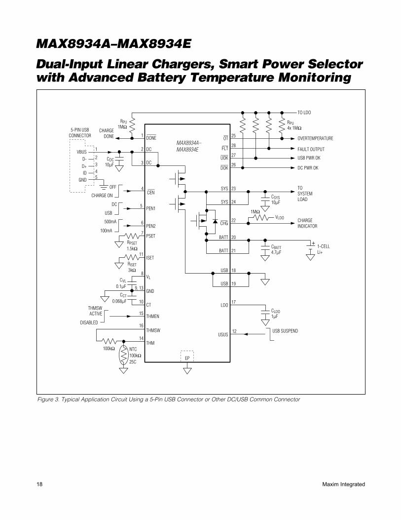
Figure 3. Typical Application Circuit Using a 5-Pin USB Connector or Other DC/USB Common Connector
DC
CHARGEDONE
5-PIN USBCONNECTOR
RPU1MI
RPU4x 1MI
CDC10FF
CSYS10FF
CBATT4.7FF
CLDO1FF
DC
PSET
VL
GND
CT
THMSW
THMSWACTIVE
DISABLED
THM
THMEN
DONE
FLT
UOK
DOK
TO LDO
VLDO
OVERTEMPERATURE
FAULT OUTPUT
USB PWR OK
DC PWR OK
TOSYSTEMLOAD
CHARGEINDICATOR
1-CELLLi+
SYS
SYS
CHG
BATT
BATT
USB
USB
LDO
USUS
EP
OT1
2
3
CEN
5
OFF
CHARGE ON
DC
VBUS
D-
D+ID
GND
USB
PEN2
PEN1
500mA
100mA
6
7
8
9, 13
10
15
16
14
4
1
2
3
45
12
17
19
USB SUSPEND
18
21
20
22
24
23
26
27
28
25
RPSET1.5kI
1MI
ISET 11
RISET3kI
100kI NTC100kI25C
CVL0.1FF
CCT0.068FF
MAX8934A–MAX8934E
19Maxim Integrated
Dual-Input Linear Chargers, Smart Power Selector with Advanced Battery Temperature Monitoring
MAX8934A–MAX8934E
Detailed DescriptionThe MAX8934_ is a dual-input linear charger with Smart Power Selector that safely charges a single Li+/Li-Poly cell in accordance with JEITA specifications*. The MAX8934_ integrates power MOSFETs and control circuitry to manage power flow in portable devices. See Figure 1. The charger has two power inputs, DC and USB. These can be separately connected to an AC adapter output and a USB port, or the DC input could be a single power input that connects to either an adapter or USB. Logic inputs, PEN1 and PEN2, select the cor-rect current limits for two-input or single-input operation. Figure 2 is the typical application circuit using separate DC and USB connectors. Figure 3 is the typical applica-tion circuit using a 5-pin USB connector or another DC/USB common connector.
In addition to charging the battery, the MAX8934_ also supplies power to the system through the SYS output. The charging current is also provided from SYS so that the set input current limit controls the total SYS current, where total SYS current is the sum of the system load current and the battery-charging current. SYS is pow-ered from either the DC input pin or the USB sources
input pin. If both the DC and USB sources are con-nected, DC takes precedence.
In some instances, there may not be enough adapter current or USB current to supply peak system loads. The MAX8934_ Smart Power Selector circuitry offers flexible power distribution from an AC adapter or USB source to the battery and system load. The battery is charged with any available power not used by the system load. If a system load peak exceeds the input current limit, supplemental current is taken from the battery. Thermal limiting prevents overheating by reducing power drawn from the input source.
The MAX8934_ features an overvoltage limiter at SYS. If the DC or USB input voltage exceeds the SYS regulation voltage, VSYS does not follow VDC or VUSB, but remains at its regulation voltage. The MAX8934_ has numerous other charging and power-management features that are detailed in the following sections.
A 3.3V ultra-low quiescent current, always-on LDO pro-vides up to 30mA for indicator LEDs and for backup power to the system. This LDO powers the thermistor monitor circuitry and provides bias to the external pullup resistor for the thermistor.
Table 1. External Components List for Figures 2 and 3
*JEITA (Japan Electronics and Information Technology Industries Association) Standard, A Guide to the Safe Use of Secondary Lithium Ion Batteries on Notebook–Type Personal Computers, April 20, 2007.
COMPONENT(Figures 2 and 3)
FUNCTION PART NUMBER
CDC DC filter capacitor10FF ±10%, 16V X5R ceramic capacitor (0805)Taiyo Yuden EMK212BJ106KG
CVL VL filter capacitor0.1FF ±10%, 10V X5R ceramic capacitor (0402)Taiyo Yuden LMK105BJ104KV
CSYS SYS output bypass capacitors10FF ±10%, 6.3V X5R ceramic capacitor (0805)Taiyo Yuden JMK212BJ106KD
CBATT Battery bypass capacitor4.7FF ±10%, 6.3V X5R ceramic capacitor (0805)Taiyo Yuden JMK212BJ475KD
CCT Charger timing capacitor0.068FF ±10%, 16V X5R ceramic capacitor (0402)Taiyo Yuden EMK105BJ683KV
CLDO LDO output capacitor1FF ±10%, 6.3V X5R ceramic capacitor (0402)Taiyo Yuden JMK105BJ105KV
RPU (x5) Logic-output pullup resistors 1MI ±5% resistor
THM Negative TC thermistor Vishay NTC Thermistor P/N NTHS0603N01N1003FF
RTHMSW THM pullup resistor 100kI
RPSET DC input current-limit programming resistor 1.5kI ±1% for 2A limit
RISET Fast-charge current programming resistor 3kI ±1% for 1A charging
20 Maxim Integrated
Dual-Input Linear Chargers, Smart Power Selector with Advanced Battery Temperature Monitoring
MAX8934A–MAX8934E
Smart Power SelectorThe MAX8934_ Smart Power Selector seamlessly distrib-utes power among the external inputs, the battery, and the system load (see the Typical Operating Circuit). The basic functions performed are:
U With both an external power supply (USB or adapter) and battery connected:
U When the system load requirements are less than the input current limit, the battery is charged with residual power from the input.
U When the system load requirements exceed the input current limit, the battery supplies supplemen-tal current to the load.
U When the battery is connected and there is no external power input, the system is powered from the battery.
U When an external power input is connected and there is no battery, the system is powered from the external power input.
A thermal-limiting circuit reduces the battery charge rate and external power-source current to prevent the MAX8934_ from overheating.
System Load SwitchAn internal 40mI MOSFET connects SYS to BATT (Q3 in the Typical Operating Circuit) when no voltage source is available at DC or USB. When an external source is detected at DC or USB, this switch is opened and SYS is powered from the valid input source through the input limiter.
The SYS-BATT switch also holds up SYS when the system load exceeds the input current limit. If that should happen, the SYS-BATT switch turns on so that the battery supplies additional SYS load current. If the system load continu-ously exceeds the input current limit, the battery does not charge, even though external power is connected. This is not expected to occur in most cases, since high loads usu-ally occur only in short peaks. During these peaks, battery energy is used, but at all other times the battery charges.
Input LimiterThe input voltage limiter is essentially an LDO regula-tor. While in dropout, the regulator dissipates a small I2R loss through the 0.2I MOSFET (Q1 in the Typical Operating Circuit) between DC and SYS. With an AC adapter or USB source connected, the input limiter distributes power from the external power source to the system load and battery charger. In addition to the input limiter’s primary function of passing power to the system
and charger loads at SYS, it performs several additional functions to optimize use of available power.
Input Voltage LimitingIf an input voltage is above the overvoltage threshold (6.9V typ), the MAX8934_ enters overvoltage lockout (OVLO). OVLO protects the MAX8934_ and downstream circuitry from high-voltage stress up to 14V at DC and 8V at USB. In OVLO, VL remains on, the input switch that sees overvoltage (Q1, Q2, Typical Operating Circuit) opens, and the appropriate power-monitor output (DOK, UOK) is high impedance, and CHG is high impedance. If both DC and USB see overvoltage, both input switches (Q1 and Q2, Typical Operating Circuit) open and the charger turns off. The BATT-to-SYS switch (Q3, Typical Operating Circuit) closes, allowing the battery to power SYS. An input is also invalid if it is less than BATT, or less than the DC undervoltage threshold of 3.5V (falling). With an invalid input voltage, SYS connects to BATT through a 40mI switch (Q3, Typical Operating Circuit).
Input Overcurrent ProtectionThe current at DC and USB is limited to prevent input overload. This current limit can be selected to match the capabilities of the source, whether it is a 100mA or 500mA USB source, or an AC adapter. When the load exceeds the input current limit, SYS drops to 75mV below BATT and the battery supplies supplemental load current.
Thermal LimitingThe MAX8934_ reduces input limiter current by 5%/NC when its die temperature exceeds +100NC. The system load (SYS) has priority over the charger current, so low-ering the charge current first reduces the input current. If the junction temperature still reaches +120NC in spite of charge current reduction, no input (DC or USB) current is drawn, the battery supplies the entire system load, and SYS is regulated at 75mV below BATT. Note that this on-chip thermal-limiting circuitry is not related to and operates independently from the thermistor input.
Adaptive Battery ChargingWhile the system is powered from DC, the charger draws power from SYS to charge the battery. If the charger load plus system load exceeds the input current limit, an adaptive charger control loop reduces charge current to prevent the SYS voltage from collapsing. Maintaining a higher SYS voltage improves efficiency and reduces power dissipation in the input limiter. The total current through the switch (Q1 or Q2 in the Typical Operating Circuit) is the sum of the load current at SYS and the battery charging current. The MAX8934A limiter clamps at 5.3V (4.35V for the MAX8934B/MAX8934C/
21Maxim Integrated
Dual-Input Linear Chargers, Smart Power Selector with Advanced Battery Temperature Monitoring
MAX8934A–MAX8934E
MAX9834D), so input voltages greater than 5.3V (4.35V for the MAX8934B/MAX8934C/MAX8934E) can increase power dissipation in the limiter. The MAX8934_ input limiter power loss is (VDC – VSYS) x IDC, where VSYS may be as high as 5.3V for the MAX8934A or 4.35V for the MAX8934B–MAX8934E. The input limiter power loss is not less than 0.2I x IDC2. Also note that the MAX8934_ turns off when any input exceeds 6.9V (typ).
DC and USB Connections and Current-Limit Options
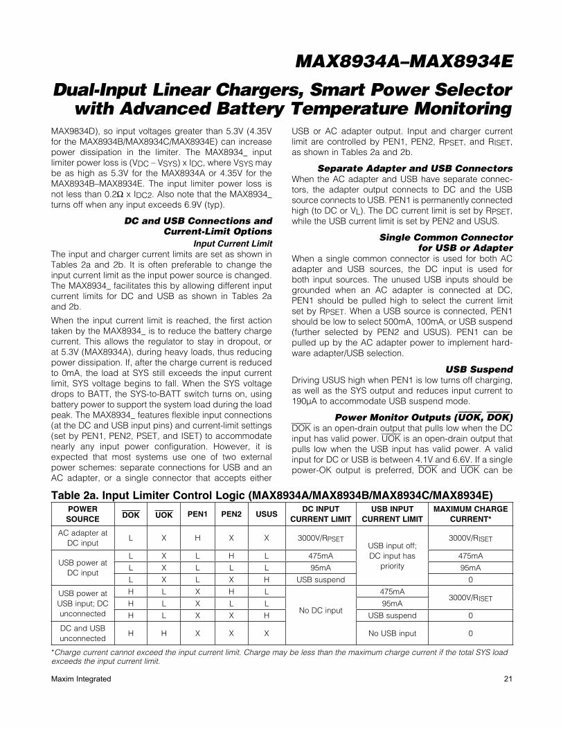
Input Current LimitThe input and charger current limits are set as shown in Tables 2a and 2b. It is often preferable to change the input current limit as the input power source is changed. The MAX8934_ facilitates this by allowing different input current limits for DC and USB as shown in Tables 2a and 2b.
When the input current limit is reached, the first action taken by the MAX8934_ is to reduce the battery charge current. This allows the regulator to stay in dropout, or at 5.3V (MAX8934A), during heavy loads, thus reducing power dissipation. If, after the charge current is reduced to 0mA, the load at SYS still exceeds the input current limit, SYS voltage begins to fall. When the SYS voltage drops to BATT, the SYS-to-BATT switch turns on, using battery power to support the system load during the load peak. The MAX8934_ features flexible input connections (at the DC and USB input pins) and current-limit settings (set by PEN1, PEN2, PSET, and ISET) to accommodate nearly any input power configuration. However, it is expected that most systems use one of two external power schemes: separate connections for USB and an AC adapter, or a single connector that accepts either
USB or AC adapter output. Input and charger current limit are controlled by PEN1, PEN2, RPSET, and RISET, as shown in Tables 2a and 2b.
Separate Adapter and USB ConnectorsWhen the AC adapter and USB have separate connec-tors, the adapter output connects to DC and the USB source connects to USB. PEN1 is permanently connected high (to DC or VL). The DC current limit is set by RPSET, while the USB current limit is set by PEN2 and USUS.
Single Common Connector for USB or Adapter
When a single common connector is used for both AC adapter and USB sources, the DC input is used for both input sources. The unused USB inputs should be grounded when an AC adapter is connected at DC, PEN1 should be pulled high to select the current limit set by RPSET. When a USB source is connected, PEN1 should be low to select 500mA, 100mA, or USB suspend (further selected by PEN2 and USUS). PEN1 can be pulled up by the AC adapter power to implement hard-ware adapter/USB selection.
USB SuspendDriving USUS high when PEN1 is low turns off charging, as well as the SYS output and reduces input current to 190FA to accommodate USB suspend mode.
Power Monitor Outputs (UOK, DOK)DOK is an open-drain output that pulls low when the DC input has valid power. UOK is an open-drain output that pulls low when the USB input has valid power. A valid input for DC or USB is between 4.1V and 6.6V. If a single power-OK output is preferred, DOK and UOK can be
Table 2a. Input Limiter Control Logic (MAX8934A/MAX8934B/MAX8934C/MAX8934E)
*Charge current cannot exceed the input current limit. Charge may be less than the maximum charge current if the total SYS load exceeds the input current limit.
POWER SOURCE DOK UOK PEN1 PEN2 USUS
DC INPUT CURRENT LIMIT
USB INPUT CURRENT LIMIT
MAXIMUM CHARGE CURRENT*
AC adapter at DC input
L X H X X 3000V/RPSETUSB input off; DC input has
priority
3000V/RISET
USB power at DC input
L X L H L 475mA 475mA
L X L L L 95mA 95mA
L X L X H USB suspend 0
USB power at USB input; DC unconnected
H L X H L
No DC input
475mA3000V/RISET
H L X L L 95mA
H L X X H USB suspend 0
DC and USB unconnected
H H X X X No USB input 0
22 Maxim Integrated
Dual-Input Linear Chargers, Smart Power Selector with Advanced Battery Temperature Monitoring
MAX8934A–MAX8934E
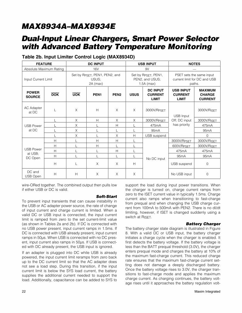
wire-ORed together. The combined output then pulls low if either USB or DC is valid.
Soft-StartTo prevent input transients that can cause instability in the USB or AC adapter power source, the rate of change of input current and charge current is limited. When a valid DC or USB input is connected, the input current limit is ramped from zero to the set current-limit value (as shown in Tables 2a and 2b). If DC is connected with no USB power present, input current ramps in 1.5ms. If DC is connected with USB already present, input current ramps in 50Fs. When USB is connected with no DC pres-ent, input current also ramps in 50Fs. If USB is connect-ed with DC already present, the USB input is ignored.
If an adapter is plugged into DC while USB is already powered, the input current limit reramps from zero back up to the DC current limit so that the AC adapter does not see a load step. During this transition, if the input current limit is below the SYS load current, the battery supplies the additional current needed to support the load. Additionally, capacitance can be added to SYS to
support the load during input power transitions. When the charger is turned on, charge current ramps from zero to the ISET current value in typically 1.5ms. Charge current also ramps when transitioning to fast-charge from prequal and when changing the USB charge cur-rent from 100mA to 500mA with PEN2. There is no dI/dt limiting, however, if ISET is changed suddenly using a switch at RISET.
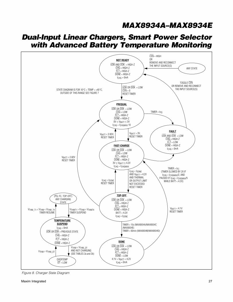
Battery ChargerThe battery charger state diagram is illustrated in Figure 8. With a valid DC or USB input, the battery charger initiates a charge cycle when the charger is enabled. It first detects the battery voltage. If the battery voltage is less than the BATT prequal threshold (3.0V), the charger enters prequal mode and charges the battery at 10% of the maximum fast-charge current. This reduced charge rate ensures that the maximum fast-charge current set-ting does not damage a deeply discharged battery. Once the battery voltage rises to 3.0V, the charger tran-sitions to fast-charge mode and applies the maximum charge current. As charging continues, the battery volt-age rises until it approaches the battery regulation volt-
Table 2b. Input Limiter Control Logic (MAX8934D)FEATURE DC INPUT USB INPUT NOTES
Absolute Maximum Rating 16V 9V —
Input Current LimitSet by RPSET, PEN1, PEN2, and
USUS;2A (max)
Set by RPSET, PEN1, PEN2, and USUS;
1.5A (max)
PSET sets the same input current limit for DC and USB
paths.
POWER SOURCE
DOK UOK PEN1 PEN2 USUSDC INPUT CURRENT
LIMIT
USB INPUT CURRENT
LIMIT
MAXIMUM CHARGE CURRENT
AC Adapter at DC
L X H X X 3000V/RPSET
USB Input Off; DC input has priority
3000V/RISET
USB Power at DC
L X H X X 3000V/RPSET 3000V/RISET
L X L H L 475mA 475mA
L X L L L 95mA 95mA
L X L X H USB suspend 0
USB Power at USB;
DC Open
H L H H L
No DC input
3000V/RPSET 3000V/RISET
H L H L L 600V/RPSET 3000V/RISET
H L L H L 475mA 475mA
H L L L L 95mA 95mA
H L X X H USB suspend 0
DC and USB Open
H H X X X No USB input 0
23Maxim Integrated
Dual-Input Linear Chargers, Smart Power Selector with Advanced Battery Temperature Monitoring
MAX8934A–MAX8934E
age where charge current starts tapering down. When charge current decreases to 10% of the fast-charge current, the charger enters a brief 15s top-off, (60min for the MAX8934B and MAX8934D) and then charging stops. If the battery voltage subsequently drops below the recharge threshold, charging restarts and the timers reset.
Charge Enable (CEN)When CEN is low, the charger is on. When CEN is high, the charger turns off. CEN does not affect the SYS out-put. In many systems, there is no need for the system controller (typically a microprocessor) to disable the charger, because the MAX8934_ Smart Power Selector circuitry independently manages charging and adapter/battery power hand-off. In these situations, CEN can be connected to ground.
Setting the Charge CurrentISET adjusts charge current to match the capacity of the battery. A resistor from ISET to ground sets the maximum fast-charge current:
ICHGMAX = 2000 x 1.5V/RISET = 3000V/RISET
Determine the ICHGMAX value by considering the char-acteristics of the battery. It is not necessary to limit the charge current based on the capabilities of the expected AC adapter/USB charging input, the system load, or thermal limitations of the PCB. The MAX8934_ automati-cally adjusts the charging algorithm to accommodate these factors.
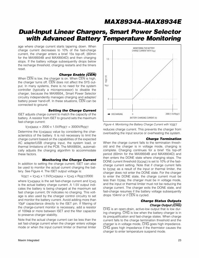
Monitoring the Charge CurrentIn addition to setting the charge current, ISET can also be used to monitor the actual current charging the bat-tery. See Figure 4. The ISET output voltage is:
VISET = ICHG x 1.5V/ICHGMAX = ICHG x RISET/2000
where ICHGMAX is the set fast-charge current and ICHG is the actual battery charge current. A 1.5V output indi-cates the battery is being charged at the maximum set fast charge current; 0V indicates no charging. This volt-age is also used by the charger control circuitry to set and monitor the battery current. Avoid adding more than 10pF capacitance directly to the ISET pin. If filtering of the charge-current monitor is necessary, add a resistor of 100kI or more between ISET and the filter capacitor to preserve charger stability.
Note that the actual charge current can be less than the set fast-charge current when the charger enters voltage mode or when the input current limiter or thermal limiter
reduces charge current. This prevents the charger from overloading the input source or overheating the system.
Charge TerminationWhen the charge current falls to the termination thresh-old and the charger is in voltage mode, charging is complete. Charging continues for a brief 15s top-off period (60min for the MAX8934B and MAX8934D) and then enters the DONE state where charging stops. The DONE current threshold (IDONE) is set to 10% of the fast-charge current setting. Note that if charge current falls to IDONE as a result of the input or thermal limiter, the charger does not enter the DONE state. For the charger to enter the DONE state, the charge current must be less than ITERM, the charger must be in voltage mode, and the input or thermal limiter must not be reducing the charge current. The charger exits the DONE state, and fast-charge resumes if the battery voltage subsequently drops 104mV or if CEN is cycled.
Charge Status OutputsCharge Output (CHG)
CHG is an open-drain, active-low output that is low dur-ing charging. CHG is low when the battery charger is in its prequalification and fast-charge states. When charge current falls to the charge termination threshold and the charger is in voltage mode, CHG goes high impedance. CHG goes high impedance if the thermistor causes the charger to enter temperature suspend mode.
Figure 4. Monitoring the Battery Charge Current with VISET
1.5
VISET
0
0 2000 (1.5V/RISET)
BATTERY CHARGING CURRENT (A)
MONITORING THE BATTERYCHARGE CURRENT WITH VISET
DISCHARGING
V ISE
T (V
)
24 Maxim Integrated
Dual-Input Linear Chargers, Smart Power Selector with Advanced Battery Temperature Monitoring
MAX8934A–MAX8934E
When the MAX8934_ is used with a microprocessor (FP), connect a pullup resistor between CHG and the logic I/O voltage to indicate charge status to the FP. Alternatively, CHG can sink up to 20mA for an LED indicator.
Charge DONE Output (DONE)DONE is an open-drain, active-low output that goes low when charging is complete. The charger enters its DONE state 15s (60min for the MAX8934B and MAX8934D) after the charge current falls to the charge-termination threshold and the charger is in voltage mode. The char-ger exits the DONE state, and fast-charge resumes, if the battery voltage subsequently drops 104mV, or if input power or CEN is cycled. When the MAX8934_ is used in conjunction with a FP, connect a pullup resistor between DONE and the logic I/O voltage to indicate charge status to the FP. Alternatively, DONE can sink up to 20mA for an LED indicator.
Fault Output (FLT) and Charge TimerFLT is an open-drain, active-low output that goes low during a battery fault. The fault state occurs when either the prequal or fast-charge timer expires. The prequal and fast-charge fault timers are set by CCT:
CTPQ
CPREQUAL: t 30min
0.068 F= ×
F
CTFC
CFAST CHARGE: t 300min
0.068 F= ×
F
TOTOP OFF: t 15s (60 minutes for the
MAX8934B and MAX8934D)
− =
While in fast-charge mode, a large system load or device self-heating can cause the MAX8934_ to reduce charge current. Under these circumstances, the fast-charge timer adjusts to ensure that adequate charge time is still allowed. Consequently, the fast-charge timer is slowed by 2x if charge current is reduced below 50% of the pro-grammed fast-charge level. If charge current is reduced to below 20% of the programmed level, the fast-charge timer is paused. The fast-charge timer is not adjusted if the charger is in voltage mode where charge current reduces due to current tapering under normal charging.
To exit a fault state, toggle CEN or remove and reconnect the input source(s). Note also that thermistor out of range or on-chip thermal-limit conditions are not considered faults. When the MAX8934_ is used in conjunction with a FP, connect a pullup resistor between FLT and the logic I/O voltage to indicate fault status to the FP. Alternatively, FLT can sink up to 20mA for an LED indicator.
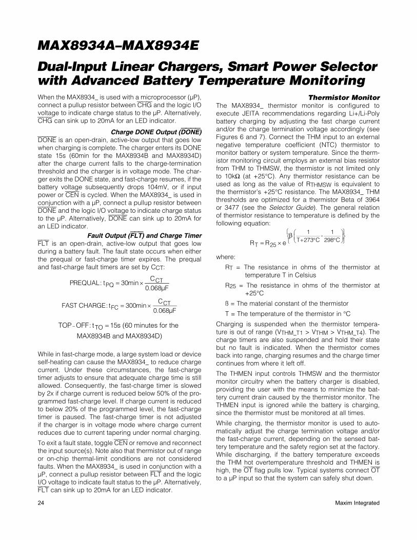
Thermistor MonitorThe MAX8934_ thermistor monitor is configured to execute JEITA recommendations regarding Li+/Li-Poly battery charging by adjusting the fast charge current and/or the charge termination voltage accordingly (see Figures 6 and 7). Connect the THM input to an external negative temperature coefficient (NTC) thermistor to monitor battery or system temperature. Since the therm-istor monitoring circuit employs an external bias resistor from THM to THMSW, the thermistor is not limited only to 10kI (at +25NC). Any thermistor resistance can be used as long as the value of RTHMSW is equivalent to the thermistor’s +25NC resistance. The MAX8934_ THM thresholds are optimized for a thermistor Beta of 3964 or 3477 (see the Selector Guide). The general relation of thermistor resistance to temperature is defined by the following equation:
1 1-
T 273 C 298 CT 25R R e
+ ° ° β
= ×
where:
RT = The resistance in ohms of the thermistor at temperature T in Celsius
R25 = The resistance in ohms of the thermistor at +25NC
A = The material constant of the thermistor
T = The temperature of the thermistor in NC
Charging is suspended when the thermistor tempera-ture is out of range (VTHM_T1 > VTHM > VTHM_T4). The charge timers are also suspended and hold their state but no fault is indicated. When the thermistor comes back into range, charging resumes and the charge timer continues from where it left off.
The THMEN input controls THMSW and the thermistor monitor circuitry when the battery charger is disabled, providing the user with the means to minimize the bat-tery current drain caused by the thermistor monitor. The THMEN input is ignored while the battery is charging, since the thermistor must be monitored at all times.
While charging, the thermistor monitor is used to auto-matically adjust the charge termination voltage and/or the fast-charge current, depending on the sensed bat-tery temperature and the safety region set at the factory. While discharging, if the battery temperature exceeds the THM hot overtemperature threshold and THMEN is high, the OT flag pulls low. Typical systems connect OT to a FP input so that the system can safely shut down.
25Maxim Integrated
Dual-Input Linear Chargers, Smart Power Selector with Advanced Battery Temperature Monitoring
MAX8934A–MAX8934E
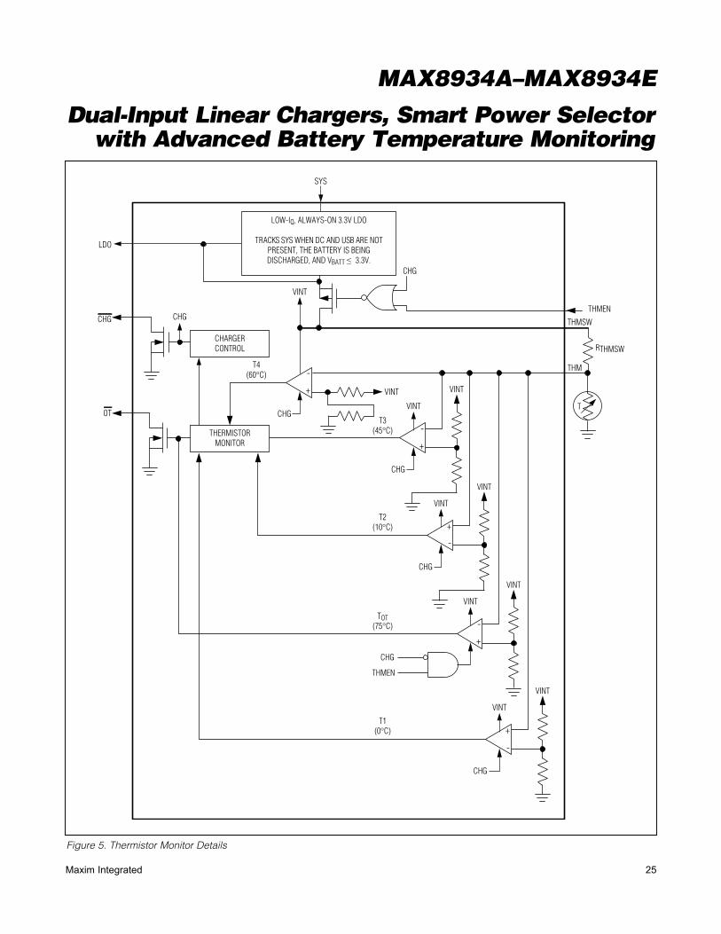
Figure 5. Thermistor Monitor Details
T
CHG
SYS
LDO
VINT
CHG
VINT
THERMISTORMONITOR
CHARGERCONTROL
CHGOT
T4(60NC)
T3(45NC)
T2(10NC)
TOT(75NC)
T1(0NC)
-
+
VINT
CHG
-
+
VINT
VINT
THM
THMSW
THMEN
RTHMSW
VINT
CHG
CHG
+
-
VINT
VINT
THMEN
CHG
-
+
VINT
VINT
+
-
CHG
LOW-IQ, ALWAYS-ON 3.3V LDO
TRACKS SYS WHEN DC AND USB ARE NOTPRESENT, THE BATTERY IS BEINGDISCHARGED, AND VBATT P 3.3V.
26 Maxim Integrated
Dual-Input Linear Chargers, Smart Power Selector with Advanced Battery Temperature Monitoring
MAX8934A–MAX8934E
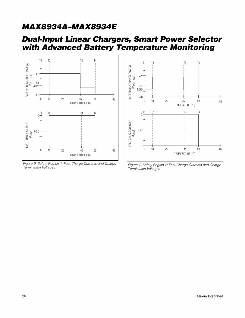
Figure 6. Safety Region 1: Fast-Charge Currents and Charge Termination Voltages
Figure 7. Safety Region 2: Fast-Charge Currents and Charge Termination Voltages
TEMPERATURE (NC)
TEMPERATURE (NC)
0
4.2
T1 T2 T3 T4
T1 T2 T3 T4
4.14.075
4.0
0.5C
C
10 25 45 60
0 10 25 45 60
85
85
BATT
REG
ULAT
ION
VOLT
AGE
(V)
(VBA
TT_R
EG)
FAST
-CHA
RGE
CURR
ENT
(I CHG
)
TEMPERATURE (NC)
TEMPERATURE (NC)
0
4.2
T1 T2 T3 T4
T1 T2 T3 T4
4.14.075
4.0
0.5C
C
10 25 45 60
0 10 25 45 60
85
85
BATT
REG
ULAT
ION
VOLT
AGE
(V)
(VBA
TT_R
EG)
FAST
-CHA
RGE
CURR
ENT
(I CHG
)
27Maxim Integrated
Dual-Input Linear Chargers, Smart Power Selector with Advanced Battery Temperature Monitoring
MAX8934A–MAX8934E
Figure 8. Charger State Diagram
STATE DIAGRAM IS FOR 10NC < TEMP < +45NC,OUTSIDE OF THIS RANGE SEE FIGURE 7
VBATT < 2.82VRESET TIMER
ICHG > IDONERESET TIMER
VBATT < 4.1VRESET TIMER
ICHG < IDONEAND VBATT = 4.2VAND THERMALOR OUTPUT LIMITNOT EXCEEDEDRESET TIMER
ANY STATE
TIMER > tPQ
TIMER > 15s (MAX8934A/MAX8934C/MAX8934E)TIMER > 60min (MAX8934B/MAX8934D)
VBATT < 2.82V,RESET TIMER
VBATT > 3V,RESET TIMER
VTHM > VTHM_OT
VTHM < VTHM_OTAND NOT CHARGING(SEE TABLES 2a and 2b)
VTHM_T1 < VTHM < VTHM_T4TIMER RESUME
VTHMT1 > VTHM > VTHMT4TIMER SUSPEND
(PQ, FC, TOP-OFF)ANY CHARGING
STATE
OVERTEMPOT = LOW
UOK OR DOK = LOWCEN = 0RESET TIMER
NOT READY
UOK AND DOK = HIGH-ZCHG = HIGH-ZFLT = HIGH-Z
DONE = HIGH-ZICHG = 0mA
PREQUAL
UOK OR DOK = LOWCHG = LOW
FLT = HIGH-ZDONE = HIGH-Z0V P VBATT P 3V
ICHG = ICHGMAX 10
FAST-CHARGE
UOK OR DOK = LOWCHG = LOW
FLT = HIGH-ZDONE = HIGH-Z
3V P VBATT P 4.2VICHG = ICHGMAX
TOP-OFF
UOK OR DOK = LOWCHG = HIGH-ZFLT = HIGH-Z
DONE = HIGH-ZBATT = 4.2VICHG = IDONE
DONE
UOK OR DOK = LOWCHG = HIGH-ZFLT = HIGH-ZDONE = LOW
4.1V < VBATT < 4.2V ICHG = 0mA
TEMPERATURESUSPENDICHG = 0mA
UOK OR DOK = PREVIOUS STATECHG = HIGH-ZFLT = HIGH-Z
DONE = HIGH-Z
CEN = HIGHORREMOVE AND RECONNECTTHE INPUT SOURCE(S)
TOGGLE CENOR REMOVE AND RECONNECT
THE INPUT SOURCE(S)
FAULT
UOK AND DOK = LOWCHG = HIGH-Z
FLT = LOWDONE = HIGH-Z
ICHG = 0mA
TIMER > tFC(TIMER SLOWED BY 2X IFICHG < ICHGMAX/2, AND
PAUSED IF ICHG < ICHGMAX/5WHILE BATT < 4.2V)
28 Maxim Integrated
Dual-Input Linear Chargers, Smart Power Selector with Advanced Battery Temperature Monitoring
MAX8934A–MAX8934E
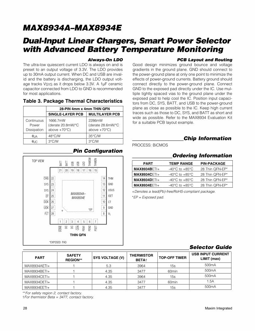
Always-On LDOThe ultra-low quiescent current LDO is always on and is preset to an output voltage of 3.3V. The LDO provides up to 30mA output current. When DC and USB are inval-id and the battery is discharging, the LDO output volt-age tracks VSYS as it drops below 3.3V. A 1FF ceramic capacitor connected from LDO to GND is recommended for most applications.
PCB Layout and RoutingGood design minimizes ground bounce and voltage gradients in the ground plane. GND should connect to the power-ground plane at only one point to minimize the effects of power-ground currents. Battery ground should connect directly to the power-ground plane. Connect GND to the exposed pad directly under the IC. Use mul-tiple tightly spaced vias to the ground plane under the exposed pad to help cool the IC. Position input capaci-tors from DC, SYS, BATT, and USB to the power-ground plane as close as possible to the IC. Keep high current traces such as those to DC, SYS, and BATT as short and wide as possible. Refer to the MAX8934 Evaluation Kit for a suitable PCB layout example.
Chip InformationPROCESS: BiCMOS
Table 3. Package Thermal Characteristics
Pin Configuration
Selector Guide
**For safety region 2, contact factory. †For thermistor Beta = 3477, contact factory.
+Denotes a lead(Pb)-free/RoHS-compliant package.
*EP = Exposed pad.
Ordering Information
28-PIN 4mm x 4mm THIN QFN
SINGLE-LAYER PCB MULTILAYER PCB
Continuous Power
Dissipation
1666.7mW(derate 20.8mW/NC above +70NC)
2286mW(derate 28.6mW/NC above +70NC)
BJA 48NC/W 35NC/W
BJC 3NC/W 3NC/W
MAX8934A–MAX8934E
THIN QFN
TOP VIEW
26
27
25
24
10
9
11
DC CEN
PEN1
PEN2
PSET
12
DONE
BATT
USB
LDO
BATT
THM
SW
THM
EN
1
*EP
*EXPOSED PAD
2
OT
4 5 6 7
2021 19 17 16 15
DOK
UOK
USUS
ISET
CT
GND
DCUS
B
3
18
28 8FLT VL
SYS
23 13 GNDSYS
22 14 THMCHG
PART TEMP RANGE PIN-PACKAGE
MAX8934BETI+ -40NC to +85NC 28 Thin QFN-EP*
MAX8934CETI+ -40NC to +85NC 28 Thin QFN-EP*
MAX8934DETI+ -40NC to +85NC 28 Thin QFN-EP*
MAX8934EETI+ -40NC to +85NC 28 Thin QFN-EP*
PARTSAFETY
REGION**SYS VOLTAGE (V)
THERMISTOR BETA† TOP-OFF TIMER
USB INPUT CURRENT LIMIT (max)
MAX8934AETI+ 1 5.3 3964 15s 500mA
MAX8934BETI+ 1 4.35 3477 60min 500mA
MAX8934CETI+ 1 4.35 3964 15s 500mA
MAX8934DETI+ 1 4.35 3477 60min 1.5A
MAX8934EETI+ 1 4.35 3477 15s 500mA
29Maxim Integrated
Dual-Input Linear Chargers, Smart Power Selector with Advanced Battery Temperature Monitoring
MAX8934A–MAX8934E
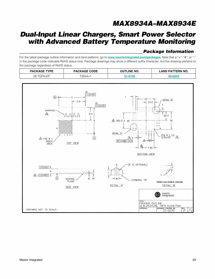
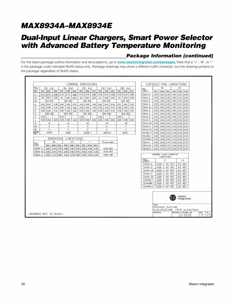
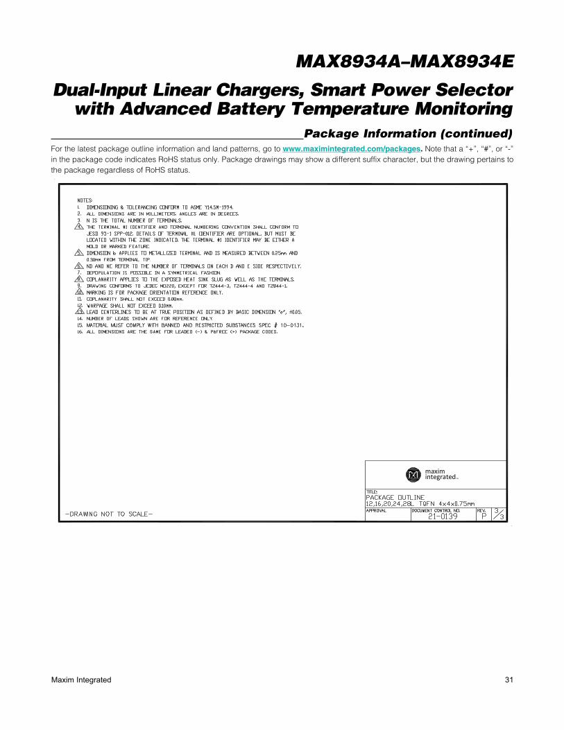
Package InformationFor the latest package outline information and land patterns, go to www.maximintegrated.com/packages. Note that a “+”, “#”, or “-” in the package code indicates RoHS status only. Package drawings may show a different suffix character, but the drawing pertains to the package regardless of RoHS status.
PACKAGE TYPE PACKAGE CODE OUTLINE NO. LAND PATTERN NO.
28 TQFN-EP T2844+1 21-0139 90-0035
30 Maxim Integrated
Dual-Input Linear Chargers, Smart Power Selector with Advanced Battery Temperature Monitoring
MAX8934A–MAX8934E
Package Information (continued)For the latest package outline information and land patterns, go to www.maximintegrated.com/packages. Note that a “+”, “#”, or “-” in the package code indicates RoHS status only. Package drawings may show a different suffix character, but the drawing pertains to the package regardless of RoHS status.
31Maxim Integrated
Dual-Input Linear Chargers, Smart Power Selector with Advanced Battery Temperature Monitoring
MAX8934A–MAX8934E
Package Information (continued)For the latest package outline information and land patterns, go to www.maximintegrated.com/packages. Note that a “+”, “#”, or “-” in the package code indicates RoHS status only. Package drawings may show a different suffix character, but the drawing pertains to the package regardless of RoHS status.
Dual-Input Linear Chargers, Smart Power Selector with Advanced Battery Temperature Monitoring
MAX8934A–MAX8934E
Maxim Integrated cannot assume responsibility for use of any circuitry other than circuitry entirely embodied in a Maxim Integrated product. No circuit patent licenses are implied. Maxim Integrated reserves the right to change the circuitry and specifications without notice at any time. The parametric values (min and max limits) shown in the Electrical Characteristics table are guaranteed. Other parametric values quoted in this data sheet are provided for guidance.
32 Maxim Integrated 160 Rio Robles, San Jose, CA 95134 USA 1-408-601-1000© 2014 Maxim Integrated Products, Inc. Maxim Integrated and the Maxim Integrated logo are trademarks of Maxim Integrated Products, Inc.
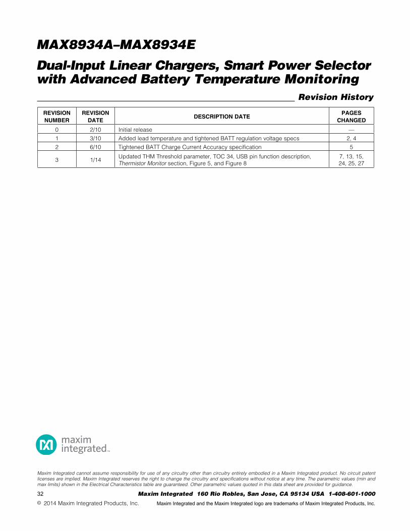
Revision History
REVISION NUMBER
REVISION DATE
DESCRIPTION DATEPAGES
CHANGED
0 2/10 Initial release —
1 3/10 Added lead temperature and tightened BATT regulation voltage specs 2, 4
2 6/10 Tightened BATT Charge Current Accuracy specification 5
3 1/14Updated THM Threshold parameter, TOC 34, USB pin function description, Thermistor Monitor section, Figure 5, and Figure 8
7, 13, 15, 24, 25, 27