Embed Size (px)
Citation preview
Maxwell–Wagner Model Analysis for the Capacitance–Voltage Characteristics
of Pentacene Field Effect Transistor
Eunju LIM, Takaaki MANAKA, Ryosuke TAMURA and Mitsumasa IWAMOTO�
Department of Physical Electronics, Tokyo Institute of Technology, 2-12-1-S3-33 O-okayama, Meguro-ku, Tokyo 152-8552, Japan
(Received September 15, 2005; revised November 22, 2005; accepted December 6, 2005; published online April 25, 2006)
The current–voltage (I–V) and capacitance–voltage (C–V) characteristics of pentacene field effect transistors (FETs) wereexamined to clarify channel formation in conjunction with the UV/ozone treatment of the source and drain metal (Au)electrodes. Analyzing the I–V and C–V characteristics of FETs using the Maxwell–Wagner model showed that the maincharge carriers in the FET channel are holes injected from the source, and that a pentacene FET with a UV/ozone-treatedsubstrate shows a high effective mobility owing to holes smoothly injected into the FET channel. Furthermore, the pentacenefilm thickness dependence on FET characteristics showed that a channel sheet with a thickness less than 20 nm is formed atthe pentacene/SiO2 interface. Finally, the employment of the Maxwell–Wagner model for the analysis of the C–Vcharacteristics was shown to give a good approximation even when taking into account the presence of a charge sheet at theinterface. [DOI: 10.1143/JJAP.45.3712]
KEYWORDS: pentacene, organic FET, UV/ozone treatment, Maxwell–Wagner model
1. Introduction
Thin-film transistors (TFTs) and light-emitting diodes(LED) using organic materials have greatly improved overthe last ten years in a number of applications including large-area flat-panel displays, radio frequency identification tags,and smart cards.1,2) Pentacene is one of the most promisingmaterials used for organic TFTs, and much experimentaleffort has been made to improve the FET performance suchas by modifying film quality.3) Along with this effort, manyanalytical studies have been devoted to understanding thedevice mechanism.4,5) For example, by measuring current–voltage (I–V) and capacitance–voltage (C–V) character-istics, we analyzed the effect of pentacene film thickness onthe performance of the field effect transistor (FET). As aresult, it has been recognized that the channel formation oforganic FETs (OFETs) is quite different from that of the so-called Si-FETs. To utilize organic devices efficiently, weneed to fully understand such a difference on the basis oforganic semiconductor physics. The energy gap between thehighest occupied molecular orbital (HOMO) and the lowestunoccupied molecular orbital (LUMO) of a pentacenemolecule is 2.6 eV;6) thus, an as-deposited pentacene filmhas a large energy gap and a very low intrinsic carrierdensity. Carrier injection and carrier doping are keyprocesses to understand the performance of pentaceneFETs.7,8) Keeping these in mind, we tried to control theelectronic structure of the organic/metal interface byadopting UV/ozone treatment. As FET characteristics arestrongly influenced by the potential barrier heights of thesource and drain electrodes, we could gain importantinsights into OFET performance in terms of carrier injection,by the UV/ozone treatment. The understanding of carriertransport is also important, and the study of the pentacenefilm thickness dependence on I–V and C–V characteristicsbecomes instructive to gain information on channel forma-tion. In our previous studies,6,9) it was revealed that thecharge carriers forming the conducting channel of pentaceneFETs are mainly injected holes from the source electrode,and that the Maxwell–Wagner model employed in analyzing
double-layer dielectric systems6) is helpful for explaining theC–V characteristics of FETs. However, details of carrierformation in the FET channel are still not clear. In thepresent paper study, we examine the I–V and C–Vcharacteristics of pentacene FETs to clarify channel for-mation in conjunction with the UV/ozone treatment of thesource and drain metal electrodes.
2. Experimental
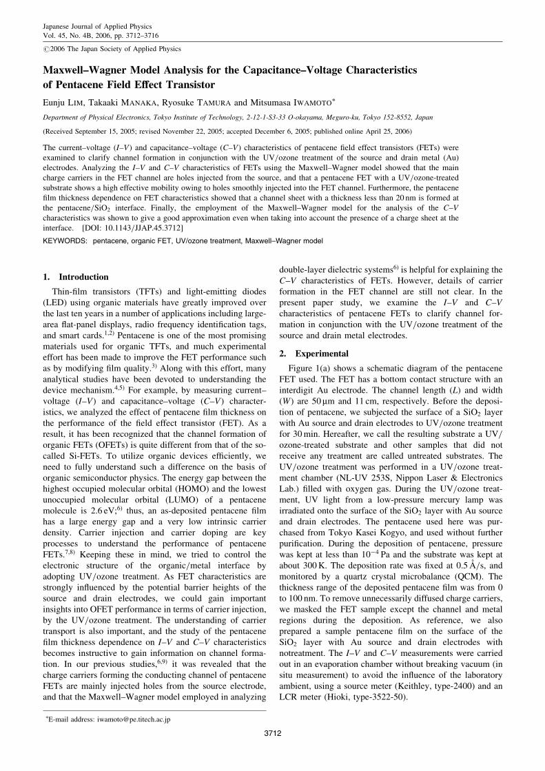
Figure 1(a) shows a schematic diagram of the pentaceneFET used. The FET has a bottom contact structure with aninterdigit Au electrode. The channel length (L) and width(W) are 50 mm and 11 cm, respectively. Before the deposi-tion of pentacene, we subjected the surface of a SiO2 layerwith Au source and drain electrodes to UV/ozone treatmentfor 30min. Hereafter, we call the resulting substrate a UV/ozone-treated substrate and other samples that did notreceive any treatment are called untreated substrates. TheUV/ozone treatment was performed in a UV/ozone treat-ment chamber (NL-UV 253S, Nippon Laser & ElectronicsLab.) filled with oxygen gas. During the UV/ozone treat-ment, UV light from a low-pressure mercury lamp wasirradiated onto the surface of the SiO2 layer with Au sourceand drain electrodes. The pentacene used here was pur-chased from Tokyo Kasei Kogyo, and used without furtherpurification. During the deposition of pentacene, pressurewas kept at less than 10�4 Pa and the substrate was kept atabout 300K. The deposition rate was fixed at 0.5 A/s, andmonitored by a quartz crystal microbalance (QCM). Thethickness range of the deposited pentacene film was from 0to 100 nm. To remove unnecessarily diffused charge carriers,we masked the FET sample except the channel and metalregions during the deposition. As reference, we alsoprepared a sample pentacene film on the surface of theSiO2 layer with Au source and drain electrodes withnotreatment. The I–V and C–V measurements were carriedout in an evaporation chamber without breaking vacuum (insitu measurement) to avoid the influence of the laboratoryambient, using a source meter (Keithley, type-2400) and anLCR meter (Hioki, type-3522-50).
�E-mail address: [email protected]
Japanese Journal of Applied Physics
Vol. 45, No. 4B, 2006, pp. 3712–3716
#2006 The Japan Society of Applied Physics
3712
3. Results and Discussion
3.1 FET characteristicsTo determine the effect of UV/ozone treatment, FET
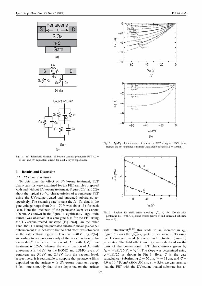
characteristics were examined for the FET samples preparedwith and without UV/ozone treatment. Figures 2(a) and 2(b)show the typical Ids–Vds characteristics of a pentacene FETusing the UV/ozone-treated and untreated substrates, re-spectively. The scanning rate to take the Ids–Vds data in thegate voltage range from 0 to �70V was about 15 s for eachscan. Here the thickness of the pentacene layer was about100 nm. As shown in the figure, a significantly large draincurrent was observed at a zero gate bias for the FET usingthe UV/ozone-treated substrate [Fig. 2(a)]. On the otherhand, the FET using the untreated substrate shows p-channelenhancement FET behavior, but no field effect was observedin the gate voltage region of less than �40V [Fig. 2(b)].According to our previous study of the work function of Auelectrodes,9) the work function of Au with UV/ozonetreatment is 5.2 eV, whereas the work function of Au withuntreatment is 4.6 eV. As the HOMO and LUMO levels ofpentacene are 5.0 eV and 2.4 eV from the vacuum level,respectively, it is reasonable to suppose that pentacene filmsdeposited on the surface with UV/ozone treatment acceptholes more smoothly than those deposited on the surface
with untreatment;10,11) this leads to an increase in Ids.Figure 3 shows the
ffiffiffiffiffiIds
p–Vg plots of pentacene FETs using
the UV/ozone-treated (curve a) and untreated (curve b)substrates. The field effect mobility was calculated on thebasis of the conventional FET characteristics given byIds ¼ W�C=2LðVg � VthÞ2. The slope was determined usingffiffiffiffiffiffiffiffiffiffiffiffiffiffiffiffiffiffiffiW�C=2L
pas shown in Fig. 3. Here, C is the gate
capacitance. Substituting L ¼ 50 mm, W ¼ 11 cm, and C ¼6:9� 10�9 F/cm2 (SiO2 500 nm, �s ¼ 3:9), we can surmisethat the FET with the UV/ozone-treated substrate has an
LS D
Gaten-SiSiO2
Pentacene
(a)
Gate
S D
G3 C3G2 C2
Go
C1
G0
G2
C1
C2
G0'
G3 C3
Gate
Source or Drain
Go'
(b)
Fig. 1. (a) Schematic diagram of bottom-contact pentacene FET (L ¼50mm) and (b) equivalent circuit for double-layer capacitance.
−40
0
−40 0
−20
−60
Vds (V)
Ids (µ
A)
Vg=−70V
Vg=0V
Vg=−60V
Vg=−50V
Vg=−40V
Vg=−30V
Vg=−20VVg=−10V
−80−60 −20
(a)
−8
−6
−4
−2
0
−40 0
Vds (V)
Vg=−40V
Ids (µ
A)
Vg=−50V
Vg=−60V
Vg=−70V
−60 −20
(b)
Fig. 2. Ids–Vds characteristics of pentacene FET using (a) UV/ozone-
treated and (b) untreated substrate (pentacene thickness d ¼ 100 nm).
−60 −40 −200
4
a
8
0
Vg (V)
Ids (m
A)
b
Fig. 3. Replots for field effect mobilityffiffiffiffiffiIds
p–Vg for 100-nm-thick
pentacene FET with UV/ozone-treated (curve a) and untreated substrate
(curve b).
Jpn. J. Appl. Phys., Vol. 45, No. 4B (2006) E. LIM et al.
3713
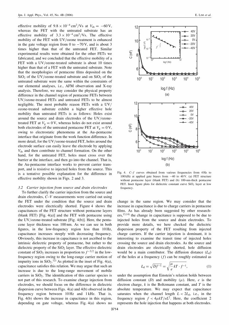
effective mobility of 9:8� 10�4 cm2/Vs at Vds ¼ �60V,whereas the FET with the untreated substrate has aneffective mobility of 3:3� 10�4 cm2/Vs. The effectivemobility of the FET with UV/ozone treatment is enhancedin the gate voltage region from 0 to �70V, and is about 3times higher than that of the untreated FET. Similarexperimental results were obtained for the other FETs wefabricated, and we concluded that the effective mobility of aFET with a UV/ozone-treated substrate is about 10 timeshigher than that of a FET with the untreated substrate. Notethat the morphologies of pentacene films deposited on theSiO2 of the UV/ozone-treated substrate and on SiO2 of theuntreated substrate were the same within the constraints ofour elemental analyses, i.e., AFM observation and X-rayanalysis. Therefore, we may consider the physical propertydifference in the channel region of pentacene FETs betweenUV/ozone-treated FETs and untreated FETs to be almostnegligible. The most probable reason FETs with a UV/ozone-treated substrate exhibit a higher effective holemobility than untreated FETs is as follows: Holes existaround the source and drain electrodes of the UV/ozone-treated FET at Vg ¼ 0V, whereas holes do not exist aroundboth electrodes of the untreated pentacene FET at Vg ¼ 0V,owing to electrostatic phenomena at the Au–pentaceneinterface that originate from the work function difference. Inmore detail, for the UV/ozone-treated FET, holes around theelectrode surface can easily leave the electrode by applyingVds and then contribute to channel formation. On the otherhand, for the untreated FET, holes must cross over thebarrier at the interface, and then go into the channel. That is,the Au-pentacene interface works to prevent carrier trans-port, and is resistive to injected holes from the source. Thisis a tentative possible explanation for the difference ineffective mobility shown in Figs. 2 and 3.
3.2 Carrier injection from source and drain electrodesTo further clarify the carrier injection from the source and
drain electrodes, C–V measurements were carried out usingthe FET under the condition that the source and drainelectrodes were electrically shorted. Figure 4 shows thecapacitances of the FET structure without pentacene layers(blank FET) [Fig. 4(a)] and the FET with pentacene usingthe UV/ozone-treated substrate [Fig. 4(b)]. Here, the penta-cene layer thickness was 100 nm. As we can see in bothfigures, in the low-frequency region less than 10Hz,capacitance increases steeply with decreasing frequency.Obviously, this increase in capacitance is not ascribed to theintrinsic dielectric property of pentacene, but rather to thedielectric property of the SiO2 layer. The effective dielectricconstant of SiO2 increases in proportion to f�3=2 in the low-frequency region owing to the long-range carrier motion ofimpurity ions in SiO2.
12) As plotted in the inset of Fig. 4(a),capacitance satisfies this relation. We may argue that such anincrease is due to the long-range movement of mobilecarriers in SiO2. The identification of this carrier species isnot part of this research. To examine charge injection fromelectrodes, we should focus on the difference in dielectricdispersion curve between Figs. 4(a) and 4(b) observed in thefrequency region between 10Hz and 1 kHz. That is,Fig. 4(b) shows the increase in capacitance in this region,depending on gate voltage, whereas Fig. 4(a) shows no
change in the same region. We may consider that theincrease in capacitance is due to charge carriers in pentacenefilms. As has already been suggested by other research-ers,13,14) the change in capacitance is supposed to be due toinjected holes from the source and drain electrodes. Toprovide more details, we here checked the dielectricdispersion property of the FET resulting from injectedcharge carriers. If the carrier injection is dominant, it isinteresting to examine the transit time of injected holescrossing the source and drain electrodes. As the source anddrain electrodes are electrically shorted, hole diffusionwould be a main contributor. The diffusion distance (Ld)of the holes at a frequency ( f ) can be roughly estimated as
Ld ¼ffiffiffiffiffiffiffiffiffiffiffiDf�1
p¼
ffiffiffiffiffiffiffiffiffiffiffiffiffiffiffiffiffiffiffiffiffi�
ekT � f�1
r; ð1Þ
under the assumption that Einstein’s relation holds betweendiffusion constant (D) and mobility (�). Here, e is theelectron charge, k is the Boltzmann constant, and T is theabsolute temperature. We may expect that capacitancesaturates when the channel length L < 2Ld, i.e., in thefrequency region f < 4�kT=eL2. Here, the coefficient 2represents the hole injection that happens at both electrodes.
20V0V
−20V −40V
40V
100 101 102 103 104 105
6
8
10
100 10110−11
10−10
10−9
f- 3
2−
12
C (n
F)
log f (Hz)
log
C (
F)
log f (Hz)(a)
100 101 102 103 104 105
6
8
10 20V
0V −20V −40V
12
C (n
F)
log f (Hz)
40V
(b)
Fig. 4. C– f curves obtained from various frequencies from 4Hz to
100 kHz at applied gate biases from �40 to 40V. (a) FET structure
without pentacene layer (blank FET) and (b) 100-nm-thick pentacene
FET. Inset figure plots for dielectric constant curve SiO2 layer at low
frequency.
Jpn. J. Appl. Phys., Vol. 45, No. 4B (2006) E. LIM et al.
3714

Substituting L ¼ 50 mm, T ¼ 300K and � ¼ 9:8� 10�4
cm2/Vs obtained from Fig. 3(a), we estimate f < 10Hz,indicating that capacitance saturates in this region. Lookingat our experimental results shown in Fig. 4(b), we find thatthe saturation of capacitance occurs in the region f < 100
Hz when Vg ¼ 0V, i.e., the cutoff frequency is 100Hz.Therefore, we may conclude that the injection of holes is areasonable process to understand the increase in capacitanceobserved in Fig. 4(b). The discrepancy between our estima-tion and experimental results possibly comes from thedifference between the measured effective mobility and thetrue mobility in the channel region. Besides, the spacecharge field effect also makes a significant contribution.Without taking into account the space charge effect, it isdifficult to explain the cutoff frequency shifts depending onapplied gate voltage in the region between 0 and �60V inFig. 4(b). That is, the difference between our experimentaldata and calculated values would reflect the space chargefield, and we may conclude that injected holes fromelectrodes are the main contributors to the increase incapacitance in the frequency region between 10Hz and1 kHz [Fig. 4(b)]. Keeping these in mind, we furtherexamine the motion of injected charges from electrodes.We measured the capacitance of the pentacene FET preparedusing the UV/ozone-treated and untreated substrates atvarious gate voltages in this frequency region.
Figure 5 shows the C–V characteristics of the pentaceneFET with the UV/ozone-treated substrate at frequencies of1 kHz (curve a1) and 43Hz (curve a2) and with the untreatedsubstrate at 1 kHz (curve b1) and 43Hz (curve b2). As shownin curve a1, capacitance increased with increasing gate biasvoltage in the region from 18 to �40V at a threshold voltage(Vth) of 18V. On the other hand, capacitance was almostconstant over the entire region for the pentacene FET withthe untreated substrate at 43Hz (curve b2), and the thresholdvoltage Vth was �20V. As mentioned above, the C–Vcharacteristics are strongly dependent on the substrate, andso only a small change was observed for the untreatedsubstrate (curve b1), possibly because very few chargecarriers are allowed to be injected into the channel. On theother hand, a drastic change was observed for the UV/ozone-treated substrate (particularly at curve a2). In the case of theFET with the untreated substrate, obviously this behavior
qualitatively corresponds to the FET characteristics, i.e., nofield effect in the low-gate-voltage region of less than�40V,whereas it smoothly increases, because the increase incapacitance corresponds to the accumulation of carriers atthe interfacial region of pentacene near the Au electrode. Tofurther clarify the accumulation of injected holes at theinterface between pentacene and the SiO2 layer, we modeledour FET using a Maxwell–Wagner capacitor as shown inFig. 1(b), where the pentacene FET was modeled using twodielectric layers. The equivalent circuit shows us that thecapacitance C is given by6)
C ¼C2G
21 þ !2C1C2ðC1 þ C2ÞG2
1 þ !2ðC1 þ C2Þ2þ C3; ð2Þ
under the assumption that the conductances G2 and G3 of theSiO2 are very low in comparison with pentacene G1 (G1 �G2, G3). Here, C1 is the capacitance between the source anddrain electrodes and the channel, and C2 is the capacitancebetween the channel and the gate electrode. G1 is the sum ofthe channel conductance G0 and bulk conductance G0
0.6) In
particular, G0 characterizes hole transport in the FETchannel, including hole injection from the electrode andtransportation in the FET channel. Taking into account thedifference in carrier injection property between the FET withthe UV/ozone-treated substrate and the FET with theuntreated substrate, we chose G1 ¼ 2 mS for the FET withthe UV/ozone-treated substrate and G1 ¼ 0:6 mS for the FETwith the untreated substrate. Note that the difference in G1
corresponds to the difference in effective mobility mentionedin §3.1. As shown in Fig. 5, the experimental results can bewell explained using the equivalent circuit model, whichindicates that the Maxwell–Wagner model described in §3.3is acceptable. A similar calculation result was also obtainedin the case assuming a ladder model instead of the equivalentcircuit model shown in Fig. 1(b) because the characteristicrelaxation time given by the bulk conductance and capaci-tance are the same. Furthermore, it is interesting to note thatthe threshold voltage Vth of the I–V characteristics shouldcorrespond to that of the C–V characteristics at a lowerfrequency. As shown in Fig. 5 threshold voltage increases asfrequency decreases, and approaches the threshold voltage ofthe I–V characteristics in Fig. 3.
3.3 Channel formation and pentacene film thicknessdependence
According to the Maxwell–Wagner double-capacitormodel, electrons (holes) injected from electrodes accumulateat the interface between the two dielectric materials, i.e.,pentacene (material 1) and SiO2 (material 2). The number ofaccumulated electrons (holes) (Qs) is proportional to thedifference in the relaxation times �1 ¼ �1=�1 and �2 ¼ �2=�2between materials 1 and 2. Here, �1 and �2 are the bulkconductivies, and �1 and �2 are the dielectric constants,respectively. For a parallel double-capacitance system, Qs isderived as
Qs ¼ Gsð�1 � �2ÞV2; ð3Þ
where G2 is the conductance of material 2 and V2 is thepotential across material 2. Applying this simple relation toour FET shown in Fig. 1(a) and assuming that theaccumulated change Qs is conveyed at a velocity of v ¼
a2
(43Hz)
a1 (1kHz)
b2 (43Hz)
b1
(1kHz)
0 20 40−20−405
6
7
Vgs (V)
C (n
F)
Fig. 5. C–V characteristics of pentacene FET using UV/ozone-treated
substrate at frequencies of 1 kHz (curve a1) and 43Hz (curve a2) and
untreated substrate at 1 kHz (curve b1) and 43Hz (curve b2).
Jpn. J. Appl. Phys., Vol. 45, No. 4B (2006) E. LIM et al.
3715

�E (�: mobility) along the interface by the external electricfield E ¼ �Vds=L applied between the source and the drain,we can derive the Ids of the FET as15)
Ids ¼ W�2
d2Vg � Vth �
1
2Vds
� �1�
�1
�2
� ��Vds
L; ð4Þ
which saturates at Vg � Vth ¼ Vds. Equation (4) is verysimilar to the basic current equation derived as a gradual-channel model equation for FETs, except for the term1� �1=�2. Therefore, from the viewpoint of the Maxwell–Wagner model, we can say that the Ids of our FETcharacteristics must be similar to the general FET character-istics, though carrier injection is the dominant process ofchannel formation. To further clarify the carrier motion ofcharges injected from the source electrode into pentacene,we examined the dependence of drain current on pentacenefilm thickness. Figure 6 shows the thickness dependence ofthe drain current of a pentacene FET using the UV/ozone-treated (curve a) and untreated substrates (curve b). For theUV/ozone-treated substrate, drain current increases withincreasing pentacene layer thickness and saturates at about130 mA at a film thickness of about 20 nm and a gate bias of�60V, indicating that charge carriers are confined withinthis region, i.e., a charge sheet with a thickness less than20 nm is formed as the channel [see Fig. 6 (curve a)]. On theother hand, the drain current Ids of the FET with theuntreated substrate is very small in comparison with the Idsof the FET with the UV/ozone-treated substrate; therefore, avery small drain current homogeneously flows into the entireregion of the pentacene, but hole injection into the FET withthe untreated substrate is more restricted by contactresistance than that into the FET with the UV/ozone-treatedsubstrate. In the inset of Fig. 6, drain current graduallyincreases in proportion to pentacene film thickness. Accord-ing to the Maxwell–Wagner model, the thickness ofaccumulated charge Qs is a priori assumed zero. However,as shown in Fig. 6 (curve a), this is not the case here, and anaccumulated charge sheet less than 20 nm thick is formed.For detailed discussion of the role of the charge carrier sheet,we need to modify our Maxwell–Wagner model, taking intoaccount contact resistance among other parameters. This isour future goal, and a theoretical study is in progress.
However, it is very instructive to show why the Maxwell–Wagner model is applicable to the equivalent circuit modelmentioned in §3.2. The presence of a charge sheet at theinterface corresponds to the presence of Cs with a thickness tof the charge sheet. Therefore, C1 corresponding to thepentacene in the equivalent circuit should be rewritten as
1
Ceff
¼1
C1
þ1
Cs
: ð5Þ
However, when the charge sheet thickness t � 20 nm, andthe pentacene layer thickness range was 100–200 nm, Cs >C1 is satisfied; this leads to the good approximationCeff � C1. This approximation supports our conclusion thatthe Maxwell–Wagner model can be applied to explain C–Vcharacteristics even in the case that a charge carrier sheet ispresent at the interface. However, to explain the details ofthe channel conductance related to a channel formation, weneed to modify the model used here, i.e., eq. (4), byintroducing a model describing organic semiconductorphysics. Further study is in progress.
4. Conclusions
Bottom contact pentacene FETs were fabricated onsubstrates with UV/ozone treatment and untreatment beforethe deposition of a pentacene layer. The I–V and C–Vcharacteristics of the fabricated FETs showed that the maincharge carriers of the FETs are holes injected from thesource electrode, and that the pentacene FET with the UV/ozone-treated substrate shows a higher effective mobilitybecause of the easy injection of holes into the FET channel.It was shown that the Maxwell–Wagner model could beemployed for the analysis of the I–V and C–V characteristicsof a FETs. The pentacene film thickness dependence on thepentacene FET characteristics showed that a channel sheetwith a thickness less than 20 nm is present at the pentacene/SiO2 interface. Finally, we showed that the C–V character-istics of FETs are explained by the Maxwell–Wagner model,even when taking into account the presence of a charge sheetat the interface.
1) C. D. Dimitrakopoulos and P. R. L. Malenfant: Adv. Mater. 14 (2002)
99.
2) K. Ziemelis: Nature (London) 393 (1998) 619.
3) S. C. Lim, S. H. Kim, J. H. Lee, M. K. Kim, D. J. Kim and T. Zyung:
Synth. Met. 148 (2005) 75.
4) C. D. Dimitrakopoulos and D. J. Mascaro: IBM J. Res. Dev. 45 (2001)
11.
5) G. Horowitz: Adv. Mater. 5 (1998) 365.
6) T. Manaka, E. Lim, R. Tamura and M. Iwamoto: Thin Solid Films 499
(2005) 386.
7) T. Yasuda, T. Goto, K. Fujita and T. Tsutsui: Appl. Phys. Lett. 85
(2004) 2098.
8) S. M. Sze: Physics of Semiconductor Devices (John Wiley & Sons,
New York, 1981).
9) Y. Suzue, T. Manaka and M. Iwamoto: Jpn. J. Appl. Phys. 44 (2005)
561.
10) D. E. King: J. Vac. Sci. Technol. A 13 (1995) 1247.
11) J. Lee, J. H. Kim and S. Im: Appl. Phys. Lett. 83 (2003) 2689.
12) M. Iwamoto: J. Appl. Phys. 77 (1995) 5314.
13) I. Torres, D. M. Taylor and E. Itoh: Appl. Phys. Lett. 85 (2004) 314.
14) S. Ogawa, T. Naijo, Y. Kimura, H. Ishii and M. Niwano: Appl. Phys.
Lett. 86 (2005) 252104.
15) E. Lim, R. Tamura, T. Manaka and M. Iwamoto: submitted to J.
Korean Phys. Soc.
0 100 200
−200
−100
0
a
b0 100 200
-0.4
-0.3
-0.2
-0.1
0
Pentacene thickness (nm)
b
Ids (µ
A)
Pentacene thickness (nm)
Ids
(µA)
Fig. 6. Thickness dependence of drain current of pentacene FET at gate
voltage of �60V using UV/ozone-treated (curve a) and untreated
substrates (curve b) (pentacene thicknesses d ¼ 0 to 100 nm). Inset figure
represents for curve b at small range.
Jpn. J. Appl. Phys., Vol. 45, No. 4B (2006) E. LIM et al.
3716


![Dinaphtho[8,1,2-cde:2',1',8'-uva]pentacene derivative and](https://img.pdfslide.net/doc/110x75/6236a3d2bc5a6b77b25c7a1e/dinaphtho812-cde218-uvapentacene-derivative-and-.jpg)
