Embed Size (px)
Citation preview
May 29, 2019
Editor's Choice Telecoms, Datacoms, Wireless, IoT
Using a COTS-based SDR platform for streamlined
5G development
By Bob Muro, application specialist, Pentek.
Commercial-off-the-shelf (COTS) software defined radio (SDR)
products have traditionally been used for military radar and communication applications because of their high performance and design flexibility.
The latest SDR products offer solutions with integrated I/O, ARM processors, and large FPGAs that include intellectual property (IP) for
accessing, routing and processing digital data.
Combining these attributes with superior signal integrity, phase-coherent sampling and multi-channel transceivers, a COTS SDR system is an ideal
choice for a 5G development platform. This article is intended to familiarise a new user with software defined radio in a multi-purpose
COTS platform that can reduce the time to market of 5G products.
Each section of this article is divided into hardware, firmware and software sub-sections for additional clarity. The hardware section is the SDR
printed circuit board (PCB) including components; firmware is internal FPGA code to create a logic design and implement digital signal processing (DSP) functions; and software is C code to control an FPGA
with firmware and to perform any additional DSP functions.
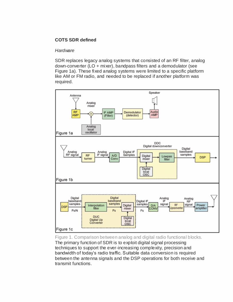
COTS SDR defined
Hardware
SDR replaces legacy analog systems that consisted of an RF filter, analog
down-converter (LO + mixer), bandpass filters and a demodulator (see Figure 1a). These fixed analog systems were limited to a specific platform like AM or FM radio, and needed to be replaced if another platform was
required.
Figure 1. Comparison between analog and digital radio functional blocks.
The primary function of SDR is to exploit digital signal processing techniques to support the ever-increasing complexity, precision and bandwidth of today’s radio traffic. Suitable data conversion is required
between the antenna signals and the DSP operations for both receive and transmit functions.
An SDR receiver converts an RF signal from an antenna into digital samples with an A/D converter and uses subsequent DSP operations to
extract the required information from the signal (see Figure 1b).
An SDR transmitter accepts digital information to be transmitted and then
performs the necessary DSP operations to produce digital samples for a D/A converter, whose analog output signal drives a power amplifier (PA) for delivery to the antenna (see Figure 1c).
Because these radios are software defined, they can be programmed on-the-fly with new parameters in microseconds, or reconfigured for many
different purposes by simply loading a new firmware image from internal or external memory.
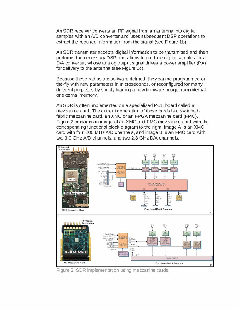
An SDR is often implemented on a specialised PCB board called a
mezzanine card. The current generation of these cards is a switched-fabric mezzanine card, an XMC or an FPGA mezzanine card (FMC).
Figure 2 contains an image of an XMC and FMC mezzanine card with the corresponding functional block diagram to the right. Image A is an XMC card with four 200 MHz A/D channels, and image B is an FMC card with
two 3,0 GHz A/D channels, and two 2,8 GHz D/A channels.
Figure 2. SDR implementation using mezzanine cards.
Each SDR board includes a precision timing system with a multi-bit, fractional synthesiser for variable sampling rates locked to an onboard
OCXO, or a reference input signal (see Figure 2). These timing systems usually accept external synchronisation signals from a network time
protocol (NTP) server or GPS receiver for the highly precise timing requirements of a radar or cellular system. The precision is also required for phase coherent sampling of the A/Ds, FPGA DSP data
synchronisation, and D/A signal transmission.
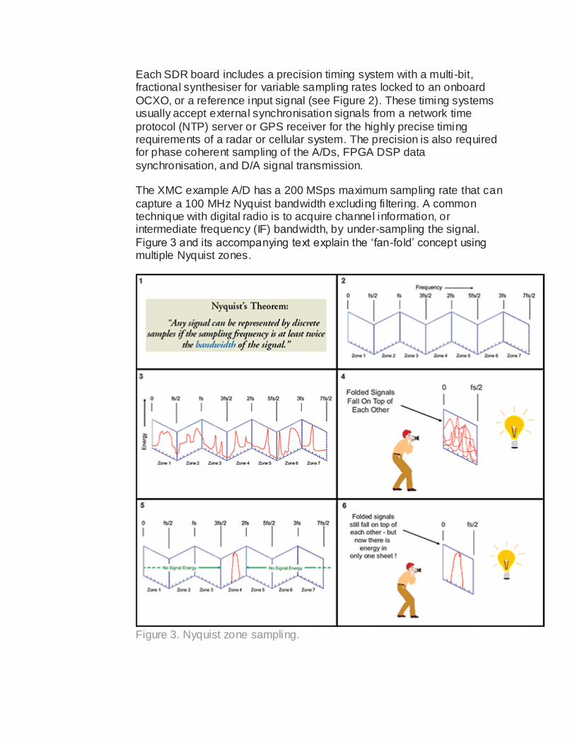
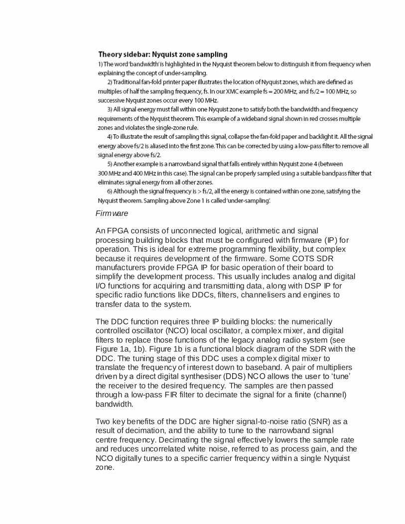
The XMC example A/D has a 200 MSps maximum sampling rate that can
capture a 100 MHz Nyquist bandwidth excluding fi ltering. A common technique with digital radio is to acquire channel information, or intermediate frequency (IF) bandwidth, by under-sampling the signal.
Figure 3 and its accompanying text explain the ‘fan-fold’ concept using multiple Nyquist zones.
Figure 3. Nyquist zone sampling.
Firmware
An FPGA consists of unconnected logical, arithmetic and signal
processing building blocks that must be configured with firmware (IP) for operation. This is ideal for extreme programming flexibility, but complex
because it requires development of the firmware. Some COTS SDR manufacturers provide FPGA IP for basic operation of their board to simplify the development process. This usually includes analog and digital
I/O functions for acquiring and transmitting data, along with DSP IP for specific radio functions like DDCs, filters, channelisers and engines to
transfer data to the system.
The DDC function requires three IP building blocks: the numerical ly controlled oscillator (NCO) local oscillator, a complex mixer, and digital
filters to replace those functions of the legacy analog radio system (see Figure 1a, 1b). Figure 1b is a functional block diagram of the SDR with the
DDC. The tuning stage of this DDC uses a complex digital mixer to translate the frequency of interest down to baseband. A pair of multipliers driven by a direct digital synthesiser (DDS) NCO allows the user to ‘tune’
the receiver to the desired frequency. The samples are then passed through a low-pass FIR filter to decimate the signal for a finite (channel)
bandwidth.
Two key benefits of the DDC are higher signal-to-noise ratio (SNR) as a result of decimation, and the ability to tune to the narrowband signal
centre frequency. Decimating the signal effectively lowers the sample rate and reduces uncorrelated white noise, referred to as process gain, and the
NCO digitally tunes to a specific carrier frequency within a single Nyquist zone.
Software
Depending upon the application, the vendor-provided FPGA IP might meet
the application specifications, but requires controlling software to operate the radio. The FPGA IP needs operational parameters sent across the
system interface from a software program. This is the function of a board support package (BSP), normally written as C programming language callable routines for a Windows or Linux OS environment. The BSP
contains library functions and pre-compiled example code that can be executed to test board functionality.
An example case for SDR is commanding the A/D to capture and transfer data to the FPGA for further processing in the DDC. This processed data can be stored to memory or transferred to the D/A section for conversion
back to an analog signal and output for transmission. This is an example of a software program developed using the BSP software library functions
and drivers. If any new FPGA IP is created by the user, then additional control software must be written for inclusion in the BSP package.
The latest COTS SDR technology
Hardware
Over the past 10 years, FPGA manufacturers like Xilinx have been
improving technology by reducing the silicon fabrication structure size, and as a result the device size, weight and power (SWaP) values were reduced. In late 2008 the Xilinx Virtex-6 family was constructed using a 40
nm process, and had an average 2000 DSP slices per FPGA.
By 2017 the Ultrascale family used a 20 nm process and the FPGA DSP
slices had increased to approximately 5,5 K. The latest system-on-chip (SoC) device from Xilinx, the RFSoC, consists of FPGA fabric with ARM processors,
A/Ds and D/As, all on the same chip. The 16 nm technology has over 4,2 K DSP slices, four 1,5 GHz A53 ARM processors, two 600 MHz R5 ARM
processors, eight 4 GHz, 12-bit A/Ds, and eight 6,4 GHz, 14-bit D/As per device. This game-changing technology can be used by COTS manufacturers to provide multi-channel SDR transceivers for engineers
developing 5G radio products.
Figure 4 is a functional block diagram of one COTS implementation of the
Xilinx RFSoC and is the central component of the 5950 3U VPX board from Pentek. The grey area is a fully connectorised RFSoC or system-on-module (SoM) that plugs into the 3U VPX carrier. This device can be
controlled via the Gigabit Ethernet port similar to the previous gene ration FPGA, but the on-board ARM processors allow autonomous operation
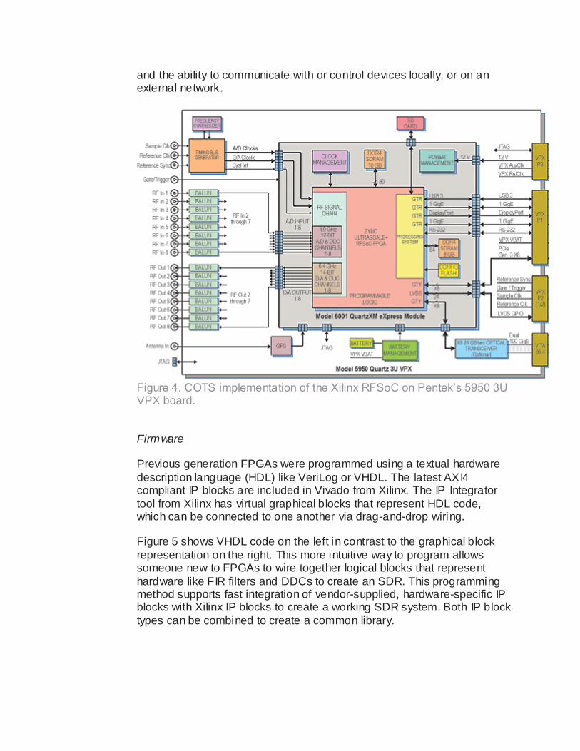
and the ability to communicate with or control devices locally, or on an external network.
Figure 4. COTS implementation of the Xilinx RFSoC on Pentek’s 5950 3U VPX board.
Firmware
Previous generation FPGAs were programmed using a textual hardware
description language (HDL) like VeriLog or VHDL. The latest AXI4 compliant IP blocks are included in Vivado from Xilinx. The IP Integrator
tool from Xilinx has virtual graphical blocks that represent HDL code, which can be connected to one another via drag-and-drop wiring.
Figure 5 shows VHDL code on the left in contrast to the graphical block
representation on the right. This more intuitive way to program allows someone new to FPGAs to wire together logical blocks that represent
hardware like FIR filters and DDCs to create an SDR. This programming method supports fast integration of vendor-supplied, hardware-specific IP blocks with Xilinx IP blocks to create a working SDR system. Both IP block
types can be combined to create a common library.
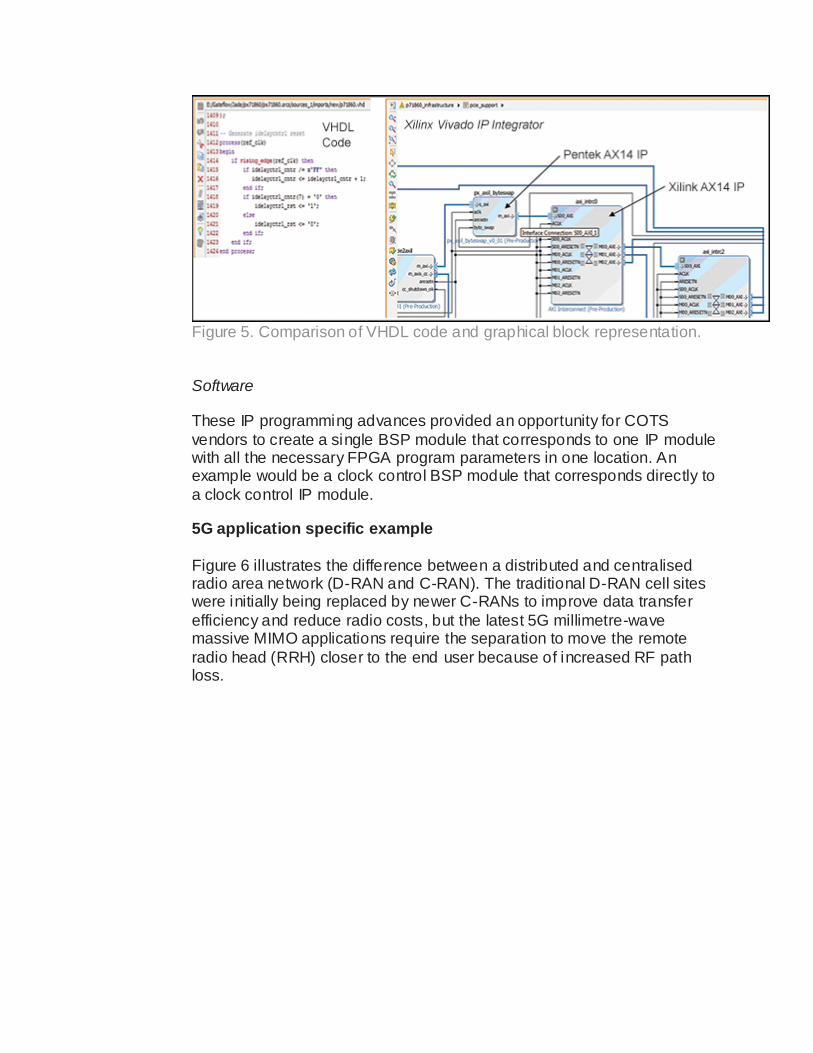
Figure 5. Comparison of VHDL code and graphical block representation.
Software
These IP programming advances provided an opportunity for COTS
vendors to create a single BSP module that corresponds to one IP module with all the necessary FPGA program parameters in one location. An example would be a clock control BSP module that corresponds directly to
a clock control IP module.
5G application specific example
Figure 6 illustrates the difference between a distributed and centralised radio area network (D-RAN and C-RAN). The traditional D-RAN cell sites were initially being replaced by newer C-RANs to improve data transfer
efficiency and reduce radio costs, but the latest 5G millimetre-wave massive MIMO applications require the separation to move the remote
radio head (RRH) closer to the end user because of increased RF path loss.
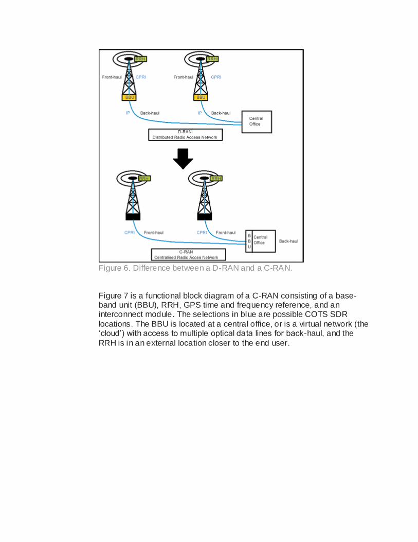
Figure 6. Difference between a D-RAN and a C-RAN.
Figure 7 is a functional block diagram of a C-RAN consisting of a base-band unit (BBU), RRH, GPS time and frequency reference, and an interconnect module. The selections in blue are possible COTS SDR
locations. The BBU is located at a central office, or is a virtual network (the ‘cloud’) with access to multiple optical data lines for back-haul, and the
RRH is in an external location closer to the end user.
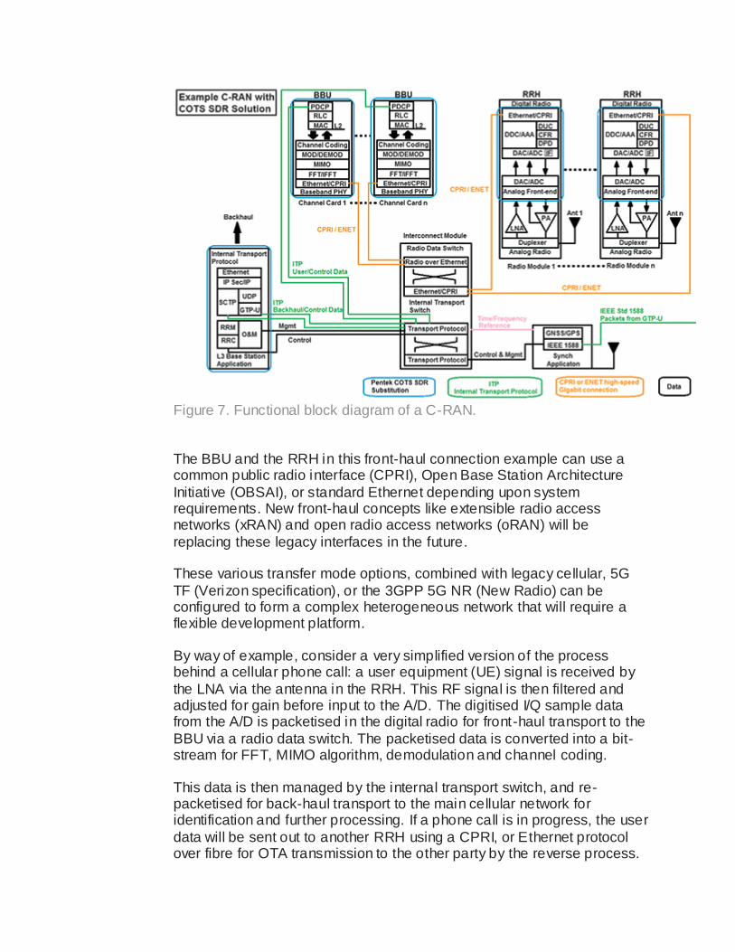
Figure 7. Functional block diagram of a C-RAN.
The BBU and the RRH in this front-haul connection example can use a common public radio interface (CPRI), Open Base Station Architecture
Initiative (OBSAI), or standard Ethernet depending upon system requirements. New front-haul concepts like extensible radio access networks (xRAN) and open radio access networks (oRAN) will be
replacing these legacy interfaces in the future.
These various transfer mode options, combined with legacy cellular, 5G
TF (Verizon specification), or the 3GPP 5G NR (New Radio) can be configured to form a complex heterogeneous network that will require a flexible development platform.
By way of example, consider a very simplified version of the process behind a cellular phone call: a user equipment (UE) signal is received by
the LNA via the antenna in the RRH. This RF signal is then filtered and adjusted for gain before input to the A/D. The digitised I/Q sample data from the A/D is packetised in the digital radio for front-haul transport to the
BBU via a radio data switch. The packetised data is converted into a bit-stream for FFT, MIMO algorithm, demodulation and channel coding.
This data is then managed by the internal transport switch, and re-packetised for back-haul transport to the main cellular network for identification and further processing. If a phone call is in progress, the user
data will be sent out to another RRH using a CPRI, or Ethernet protocol over fibre for OTA transmission to the other party by the reverse process.
Hardware
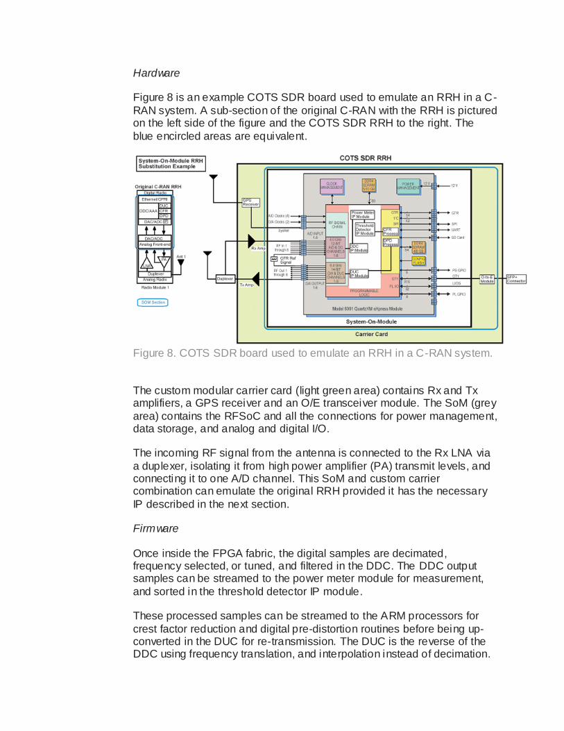
Figure 8 is an example COTS SDR board used to emulate an RRH in a C-
RAN system. A sub-section of the original C-RAN with the RRH is pictured on the left side of the figure and the COTS SDR RRH to the right. The
blue encircled areas are equivalent.
Figure 8. COTS SDR board used to emulate an RRH in a C-RAN system.
The custom modular carrier card (light green area) contains Rx and Tx amplifiers, a GPS receiver and an O/E transceiver module. The SoM (grey
area) contains the RFSoC and all the connections for power management, data storage, and analog and digital I/O.
The incoming RF signal from the antenna is connected to the Rx LNA via
a duplexer, isolating it from high power amplifier (PA) transmit levels, and connecting it to one A/D channel. This SoM and custom carrier combination can emulate the original RRH provided it has the necessary
IP described in the next section.
Firmware
Once inside the FPGA fabric, the digital samples are decimated, frequency selected, or tuned, and filtered in the DDC. The DDC output samples can be streamed to the power meter module for measurement,
and sorted in the threshold detector IP module.
These processed samples can be streamed to the ARM processors for
crest factor reduction and digital pre-distortion routines before being up-converted in the DUC for re-transmission. The DUC is the reverse of the DDC using frequency translation, and interpolation instead of decimation.
The digitised I/Q sample data is packetised in the digital radio for transport to the BBU via a radio data switch, as in the sidebar description of a
cellular phone call. Because of the variety of channels and data transfer protocols, it is necessary to calculate the maximum data throughput of
your signal.
Ignoring encoding variations, an RRH with two antennas and a 5 MHz LTE channel bandwidth will have the following data transfer requirements:
• The 5 MHz channel requires at least 10 MHz sampling, or 10 MSps, to capture the information. There are two Bytes per 16-bit sample and two
samples for I and Q.
• SRmax (maximum sampling rate) = 5 MSps x 2 Bytes/sample x 2 for I and Q = 20 MBps x 8 bits/Byte = 160 Mbps per antenna.
• Two antenna inputs = 160 Mbps x 2 = 320 Mbps of data throughput and no issue for a CPRI port with a 10 to 25 Gbps capacity.
By comparison, a new 5G link with a
100 MHz channel and 8 antenna inputs increases the data transfer requirement to around 52 Gbps, requiring multiple CPRI ports.
Software
Depending upon the desired level of control, either BSP routines need to
be created for the new IP and ARM processors, or the ARM processors in conjunction with the FPGA can be programmed to operate autonomously.
Conclusion
The purpose of this article was to familiarise a traditional radio engineer with the latest hardware, firmware, software and design tools available
from COTS vendors to create an SDR system that can be used for a 5G development platform. These SDR platforms provide superior signal integrity performance, high test repeatability and modular assemblies that
adjust to constantly changing 5G design requirements.
Future 5G implementations will require many development platforms for
experimentation, and the use of a COTS system as a starting point will ensure an accelerated time-to-market.
https://www.dataweek.co.za/9473a