Embed Size (px)
Citation preview
©Macroblock, Inc. 2009 Floor 6-4, No.18, Pu-Ting Rd., Hsinchu, Taiwan 30077, ROC.
TEL: +886-3-579-0068, FAX: +886-3-579-7534 E-mail: [email protected] - 1 -
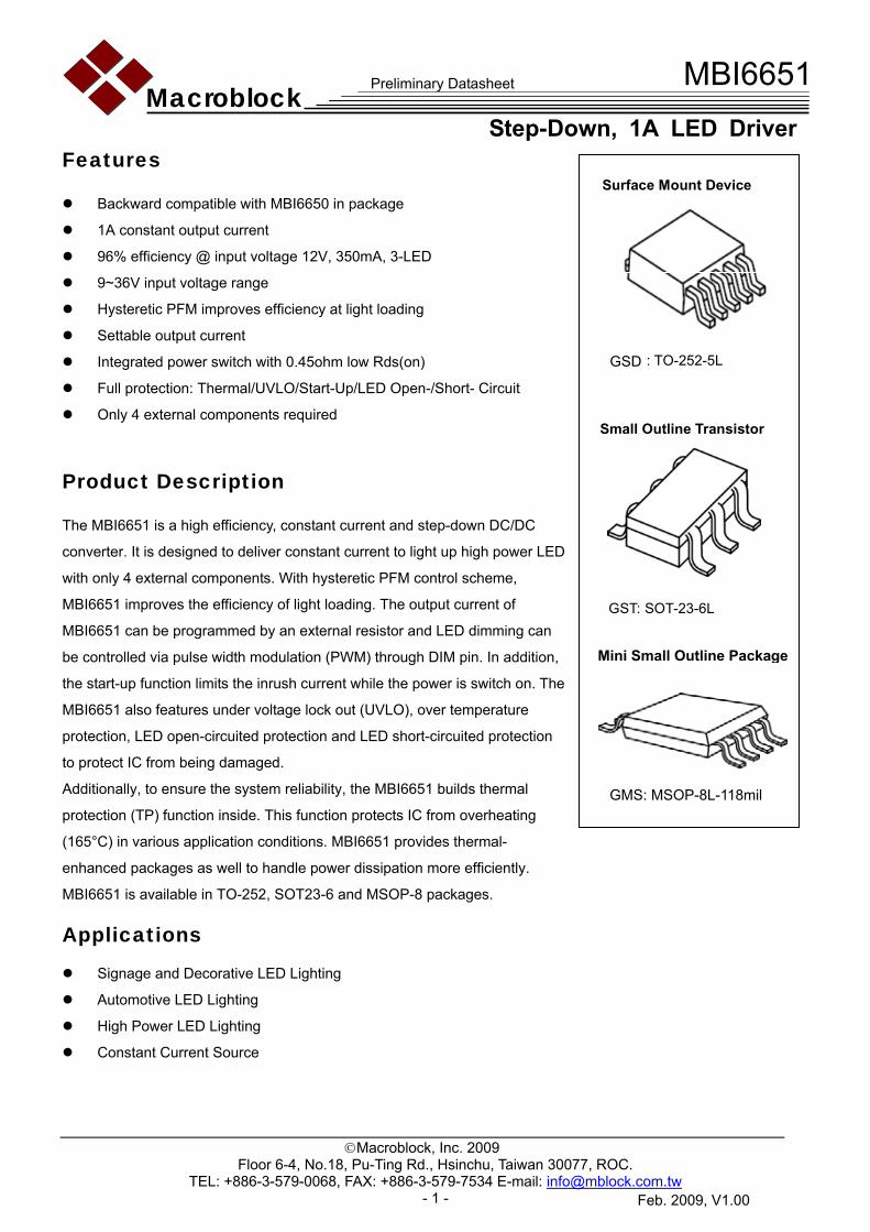
Macroblock Preliminary Datasheet MBI6651
Step-Down, 1A LED Driver
Feb. 2009, V1.00
Features
Backward compatible with MBI6650 in package
1A constant output current
96% efficiency @ input voltage 12V, 350mA, 3-LED
9~36V input voltage range
Hysteretic PFM improves efficiency at light loading
Settable output current
Integrated power switch with 0.45ohm low Rds(on)
Full protection: Thermal/UVLO/Start-Up/LED Open-/Short- Circuit
Only 4 external components required
Product Description
The MBI6651 is a high efficiency, constant current and step-down DC/DC
converter. It is designed to deliver constant current to light up high power LED
with only 4 external components. With hysteretic PFM control scheme,
MBI6651 improves the efficiency of light loading. The output current of
MBI6651 can be programmed by an external resistor and LED dimming can
be controlled via pulse width modulation (PWM) through DIM pin. In addition,
the start-up function limits the inrush current while the power is switch on. The
MBI6651 also features under voltage lock out (UVLO), over temperature
protection, LED open-circuited protection and LED short-circuited protection
to protect IC from being damaged.
Additionally, to ensure the system reliability, the MBI6651 builds thermal
protection (TP) function inside. This function protects IC from overheating
(165°C) in various application conditions. MBI6651 provides thermal-
enhanced packages as well to handle power dissipation more efficiently.
MBI6651 is available in TO-252, SOT23-6 and MSOP-8 packages.
Applications
Signage and Decorative LED Lighting
Automotive LED Lighting
High Power LED Lighting
Constant Current Source
Small Outline Transistor
GST: SOT-23-6L
PSD: TO-252-5L
Surface Mount Device
Mini Small Outline Package
GMS: MSOP-8L-118mil
GSD
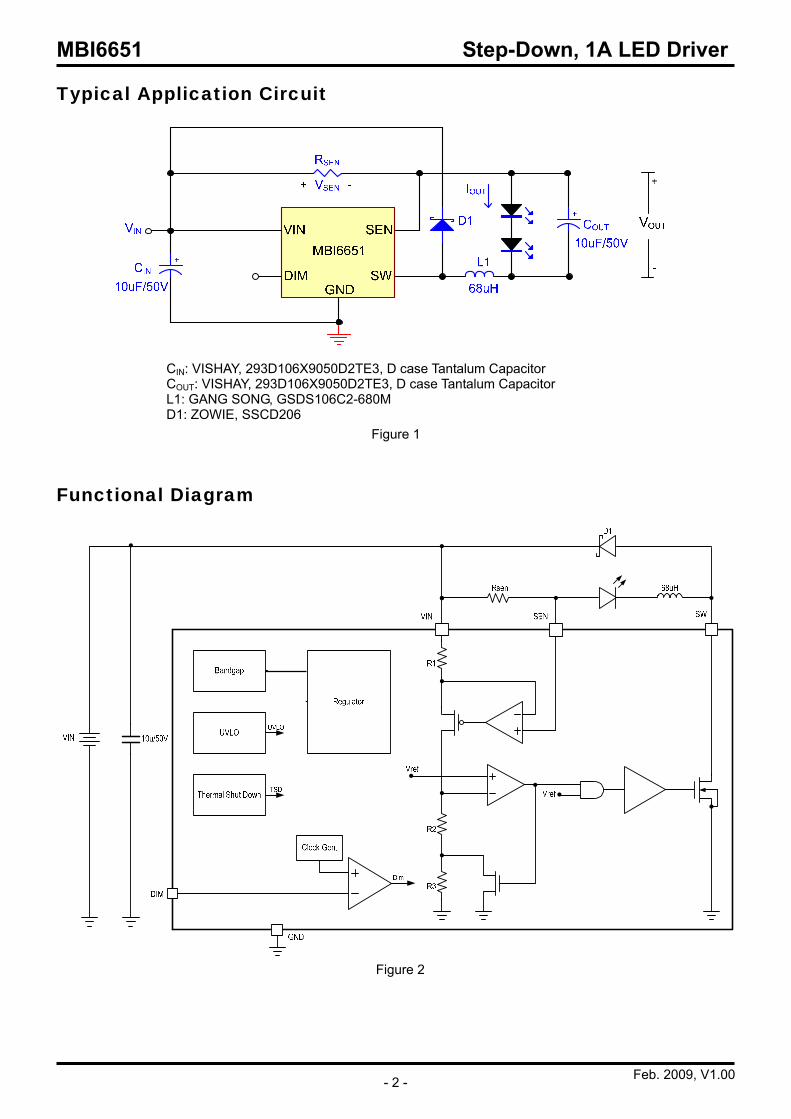
MBI6651 Step-Down, 1A LED Driver
Feb. 2009, V1.00 - 2 -
Typical Application Circuit
CIN: VISHAY, 293D106X9050D2TE3, D case Tantalum Capacitor COUT: VISHAY, 293D106X9050D2TE3, D case Tantalum Capacitor L1: GANG SONG, GSDS106C2-680M D1: ZOWIE, SSCD206
Figure 1
Functional Diagram
Figure 2
MBI6651 Step-Down, 1A LED Driver
Feb. 2009, V1.00 - 3 -
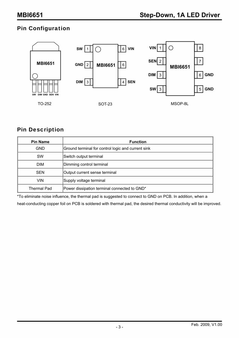
Pin Configuration
Pin Description
*To eliminate noise influence, the thermal pad is suggested to connect to GND on PCB. In addition, when a
heat-conducting copper foil on PCB is soldered with thermal pad, the desired thermal conductivity will be improved.
Pin Name Function GND Ground terminal for control logic and current sink
SW Switch output terminal
DIM Dimming control terminal
SEN Output current sense terminal
VIN Supply voltage terminal
Thermal Pad Power dissipation terminal connected to GND*
1
2
3
8
7
6
VIN
SEN
DIM GND
MBI6651
3 5SW GND
TO-252 SOT-23 MSOP-8L
MBI6651
SW DIM GND SEN VIN
1
2
3
6
6
4
SW
GND
DIM
VIN
SEN
MBI6651
MBI6651 Step-Down, 1A LED Driver
Feb. 2009, V1.00 - 4 -
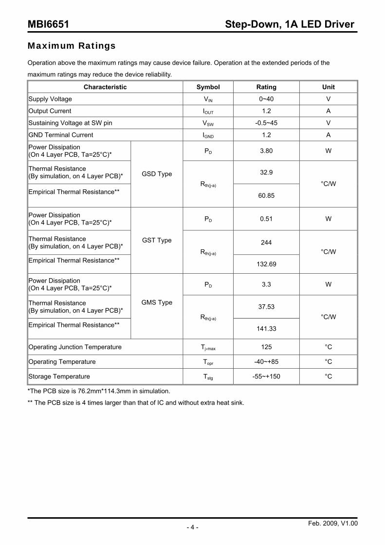
Maximum Ratings
Operation above the maximum ratings may cause device failure. Operation at the extended periods of the
maximum ratings may reduce the device reliability.
Characteristic Symbol Rating Unit
Supply Voltage VIN 0~40 V
Output Current IOUT 1.2 A
Sustaining Voltage at SW pin VSW -0.5~45 V
GND Terminal Current IGND 1.2 A
Power Dissipation (On 4 Layer PCB, Ta=25°C)* PD 3.80 W
Thermal Resistance (By simulation, on 4 Layer PCB)* 32.9
Empirical Thermal Resistance**
GSD Type Rth(j-a)
60.85
°C/W
Power Dissipation (On 4 Layer PCB, Ta=25°C)* PD 0.51 W
Thermal Resistance (By simulation, on 4 Layer PCB)* 244
Empirical Thermal Resistance**
GST Type
Rth(j-a)
132.69
°C/W
Power Dissipation (On 4 Layer PCB, Ta=25°C)* PD 3.3 W
Thermal Resistance (By simulation, on 4 Layer PCB)* 37.53
Empirical Thermal Resistance**
GMS Type
Rth(j-a)
141.33
°C/W
Operating Junction Temperature Tj,max 125 °C
Operating Temperature Topr -40~+85 °C
Storage Temperature Tstg -55~+150 °C
*The PCB size is 76.2mm*114.3mm in simulation.
** The PCB size is 4 times larger than that of IC and without extra heat sink.
MBI6651 Step-Down, 1A LED Driver
Feb. 2009, V1.00 - 5 -
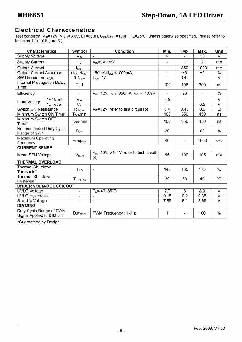
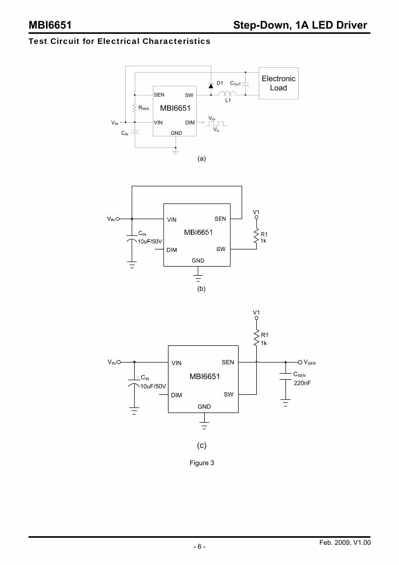
Electrical Characteristics Test condition: VIN=12V, VOUT=3.6V, L1=68µH, CIN=COUT=10µF, TA=25°C; unless otherwise specified. Please refer to test circuit (a) of Figure 3.)
Characteristics Symbol Condition Min. Typ. Max. Unit Supply Voltage VIN - 9 - 36 V Supply Current IIN VIN=9V~36V - 1 2 mA Output Current IOUT - - 350 1000 mA Output Current Accuracy dIOUT/IOUT 150mA≤IOUT≤1000mA, - ±3 ±5 % SW Dropout Voltage VSW IOUT=1A - 0.45 - V Internal Propagation Delay Time Tpd 100 196 300 ns
Efficiency - VIN=12V, IOUT=350mA, VOUT=10.8V - 96 - % “H” level VIH - 3.5 - - V Input Voltage “L” level VIL - - - 0.5 V
Switch ON Resistance Rds(on) VIN=12V; refer to test circuit (b) 0.4 0.45 0.6 Ω Minimum Switch ON Time* TON,min 100 350 450 ns Minimum Switch OFF Time* TOFF,min 100 350 450 ns Recommended Duty Cycle Range of SW* Dsw 20 - 80 %
Maximum Operating frequency FreqMax 40 - 1000 kHz
CURRENT SENSE
Mean SEN Voltage VSEN VIN=10V, V1=1V, refer to test circuit (c) 95 100 105 mV
THERMAL OVERLOAD Thermal Shutdown Threshold* TSD - 145 165 175 °C
Thermal Shutdown Hystersis* TSD-HYS - 20 30 40 °C
UNDER VOLTAGE LOCK OUT UVLO Voltage - TA=-40~85°C 7.7 8 8.3 V UVLO Hysteresis - - 0.15 0.2 0.35 V Start Up Voltage - - 7.85 8.2 8.65 V DIMMING Duty Cycle Range of PWM Signal Applied to DIM pin DutyDIM PWM Frequency : 1kHz 1 - 100 %
*Guaranteed by Design.
MBI6651 Step-Down, 1A LED Driver
Feb. 2009, V1.00 - 6 -
Test Circuit for Electrical Characteristics
MBI6651
VIN
SEN SW
DIM
GND
VIN
Electronic Load
VIH
VIL
L1
D1 COUT
CIN
RSEN
(a)
(b)
VIN
DIM SW
SEN
GND
MBI6651+ CINCSEN
VIN VSEN
V1
R11k
220nF10uF/50V
(c)
Figure 3
MBI6651 Step-Down, 1A LED Driver
Feb. 2009, V1.00 - 7 -
Typical Performance Characteristics Please refer to Typical Application Circuit, VIN=12V, L1=68uH, CIN=COUT=10uF, TA=25°C, unless otherwise specified.
1-LED VF=3.6V; 2-LED VF=7.2V; 3-LED VF=10.8V; 4-LED VF=14.4V; 5-LED VF=18V
1. Efficiency vs. Input Voltage at Various LED Cascaded Numbers Efficiency vs. input voltage @ L1=22uH
70%
75%
80%
85%
90%
95%
100%
9 12 15 18 21 24 27 30 33 36Input Voltage (V)
Effic
ienc
y (%
)
RSEN=0.1ΩL1=22uHCIN=COUT=10uF
1-LED
2-LED
3-LED4-LED5-LED6-LED
70%
75%
80%
85%
90%
95%
100%
9 12 15 18 21 24 27 30 33 36Input Voltage (V)
Effic
ienc
y (%
)
RSEN=0.135ΩL1=22uHCIN=COUT=10uF
1-LED2-LED
3-LED
4-LED5-LED6-LED
IOUT=1A
Efficiency vs. input voltage @ L1=68uH
70%
75%
80%
85%
90%
95%
100%
9 12 15 18 21 24 27 30 33 36Input Voltage (V)
Effic
ienc
y (%
)
RSEN=0.1ΩL1=68uHCIN=COUT=10uF
1-LED
2-LED
3-LED4-LED5-LED6-LED
70%
75%
80%
85%
90%
95%
100%
9 12 15 18 21 24 27 30 33 36Input Voltage (V)
Effic
ienc
y (%
)
RSEN=0.135ΩL1=68uHCIN=COUT=10uF
1-LED
2-LED
3-LED4-LED5-LED6-LED
IOUT=1A
Efficiency vs. input voltage @ L1=100uH
70%
75%
80%
85%
90%
95%
100%
9 12 15 18 21 24 27 30 33 36Input Voltage (V)
Effic
ienc
y (%
)
RSEN=0.1ΩL1=100uHCIN=COUT=10uF
1-LED
2-LED
3-LED4-LED5-LED6-LED
70%
75%
80%
85%
90%
95%
100%
9 12 15 18 21 24 27 30 33 36Input Voltage (V)
Effic
ienc
y (%
)
RSEN=0.135ΩL1=100uHCIN=COUT=10uF
1-LED
2-LED
3-LED4-LED5-LED6-LED
70%
75%
80%
85%
90%
95%
100%
9 12 15 18 21 24 27 30 33 36Input Voltage (V)
Effic
ienc
y (%
)
RSEN=0.27ΩL1=22uHCIN=COUT=10uF
1-LED
2-LED
3-LED
4-LED5-LED6-LED
IOUT=370mA IOUT=740mA
70%
75%
80%
85%
90%
95%
100%
9 12 15 18 21 24 27 30 33 36Input Voltage (V)
Effic
ienc
y (%
)
RSEN=0.27ΩL1=68uHCIN=COUT=10uF
1-LED2-LED
3-LED
4-LED5-LED6-LED
IOUT=370mA IOUT=740mA
IOUT=740mA
70%
75%
80%
85%
90%
95%
100%
9 12 15 18 21 24 27 30 33 36Input Voltage (V)
Effic
ienc
y (%
)
RSEN=0.27ΩL1=100uHCIN=COUT=10uF
1-LED
2-LED
3-LED
4-LED5-LED6-LED
IOUT=370mA IOUT=1A
MBI6651 Step-Down, 1A LED Driver
Feb. 2009, V1.00 - 8 -
2. Efficiency vs. LED Cascaded Number at Various Input Voltage
Efficiency vs. LED cascaded number @ L1=22uH
75%
80%
85%
90%
95%
100%
1 2 3 4 5 6 7LED Cascaded Number
Effic
ienc
y (%
)
RSEN=0.1ΩL1=22uHCIN=COUT=10uF
12VIN
24VIN
36VIN9VIN
75%
80%
85%
90%
95%
100%
1 2 3 4 5 6 7LED Cascaded Number
Effic
ienc
y (%
)
RSEN=0.135ΩL1=22uHCIN=COUT=10uF
12VIN
24VIN
36VIN9VIN
IOUT=1A IOUT=740mA
Efficiency vs. LED cascaded number @ L1=68uH
75%
80%
85%
90%
95%
100%
1 2 3 4 5 6 7LED Cascaded Number
Effi
cien
cy (%
)
RSEN=0.1ΩL1=68uHCIN=COUT=10uF
12VIN
24VIN
36VIN
9VIN
75%
80%
85%
90%
95%
100%
1 2 3 4 5 6 7LED Cascaded Number
Effic
ienc
y (%
)
RSEN=0.135ΩL1=68uHCIN=COUT=10uF
12VIN24VIN
36VIN9VIN
IOUT=1A IOUT=740mA
Efficiency vs. LED cascaded number @ L1=100uH
75%
80%
85%
90%
95%
100%
1 2 3 4 5 6 7LED Cascaded Number
Effi
cien
cy (%
)
RSEN=0.1ΩL1=100uHCIN=COUT=10uF
12VIN
24VIN
36VIN
9VIN
IOUT=1A
75%
80%
85%
90%
95%
100%
1 2 3 4 5 6 7LED Cascaded Number
Effi
cien
cy (%
)
RSEN=0.135ΩL1=100uHCIN=COUT=10uF
12VIN24VIN
36VIN9VIN
75%
80%
85%
90%
95%
100%
1 2 3 4 5 6 7LED Cascaded Number
Effi
cien
cy (%
)
RSEN=0.27ΩL1=22uHCIN=COUT=10uF
12VIN 24VIN
36VIN9VIN
IOUT=370mA
IOUT=370mA
75%
80%
85%
90%
95%
100%
1 2 3 4 5 6 7LED Cascaded Number
Effic
ienc
y (%
)
RSEN=0.27ΩL1=68uHCIN=COUT=10uF
12VIN 24VIN
36VIN
9VIN
75%
80%
85%
90%
95%
100%
1 2 3 4 5 6 7LED Cascaded Number
Effic
ienc
y (%
)
RSEN=0.27ΩL1=100uHCIN=COUT=10uF
12VIN 24VIN
36VIN9VIN
IOUT=370mA IOUT=740mA
MBI6651 Step-Down, 1A LED Driver
Feb. 2009, V1.00 - 9 -
3. Output Current vs. Input Voltage at Various LED Cascaded Numbers
Output current vs. input voltage @ L1=22uH
930
940
950
960
970
980
990
1000
1010
1020
1030
9 12 15 18 21 24 27 30 33 36Input Voltage (V)
Out
put C
urre
nt (m
A)
RSEN=0.1ΩL1=22uHCIN=COUT=10uF
1-LED
2-LED 3-LED4-LED5-LED6-LED
680
700
720
740
760
780
800
820
9 12 15 18 21 24 27 30 33 36Input Voltage (V)
Out
put C
urre
nt (m
A)
RSEN=0.135ΩL1=22uHCIN=COUT=10uF
1-LED
2-LED
3-LED 4-LED5-LED6-LED
Output current vs. input voltage @ L1=68uH
960
965
970
975
980
985
990
995
1000
9 12 15 18 21 24 27 30 33 36Input Voltage (V)
Out
put C
urre
nt (m
A)
RSEN=0.1ΩL1=68uHCIN=COUT=10uF
1-LED
2-LED
3-LED
4-LED
5-LED 6-LED690
695
700
705
710
715
720
725
730
735
740
745
9 12 15 18 21 24 27 30 33 36Input Voltage (V)
Out
put C
urre
nt (m
A)
RSEN=0.135ΩL1=68uHCIN=COUT=10uF
1-LED
2-LED3-LED 4-LED
5-LED6-LED
Output current vs. input voltage @ L1=100uH
950
955
960
965
970
975
980
9 12 15 18 21 24 27 30 33 36Input Voltage (V)
Out
put C
urre
nt (m
A)
RSEN=0.1ΩL1=100uHCIN=COUT=10uF
1-LED
2-LED
3-LED
4-LED5-LED 6-LED
720
725
730
735
740
745
9 12 15 18 21 24 27 30 33 36Input Voltage (V)
Out
put C
urre
nt (m
A)
RSEN=0.135ΩL1=100uHCIN=COUT=10uF
1-LED
2-LED
3-LED4-LED5-LED 6-LED
300
320
340
360
380
400
420
440
460
9 12 15 18 21 24 27 30 33 36Input Voltage (V)
Out
put C
urre
nt (m
A)
RSEN=0.27ΩL1=22uHCIN=COUT=10uF
1-LED
2-LED
3-LED
4-LED5-LED
6-LED
IOUT=370mA
330
340
350
360
370
380
390
9 12 15 18 21 24 27 30 33 36Input Voltage (V)
Out
put C
urre
nt (m
A)
RSEN=0.27ΩL1=68uHCIN=COUT=10uF
1-LED
2-LED
3-LED
4-LED
5-LED
6-LED
IOUT=370mA
350
355
360
365
370
375
380
385
390
9 12 15 18 21 24 27 30 33 36Input Voltage (V)
Out
put C
urre
nt (m
A)
RSEN=0.27ΩL1=100uHCIN=COUT=10uF
1-LED
2-LED3-LED
4-LED5-LED6-LED
IOUT=370mA
IOUT=740mA IOUT=1A
IOUT=1A IOUT=740mA
IOUT=1A IOUT=740mA
MBI6651 Step-Down, 1A LED Driver
Feb. 2009, V1.00 - 10 -
4. Output Current vs. Input Voltage at Various Inductors
Output current vs. input voltage @ 1-LED in cascaded
950
960
970
980
990
1000
1010
1020
1030
9 12 15 18 21 24 27 30 33 36
Input Voltage (V)
Out
put C
urre
nt (m
A)
RSEN=0.1Ω1-LED in CascadedCIN=COUT=10uF
22uH
68uH
100uH
700
720
740
760
780
800
820
9 12 15 18 21 24 27 30 33 36
Input Voltage (V)
Out
put C
urre
nt (m
A)
RSEN=0.135Ω1-LED in CascadedCIN=COUT=10uF
22uH
68uH
100uH
Output current vs. input voltage @ 2-LED in cascaded
950
960
970
980
990
1000
1010
9 12 15 18 21 24 27 30 33 36
Input Voltage (V)
Out
put C
urre
nt (m
A)
RSEN=0.1Ω2-LED in CascadedCIN=COUT=10uF
22uH
68uH
100uH
700
710
720
730
740
750
760
770
780
790
800
9 12 15 18 21 24 27 30 33 36
Input Voltage (V)
Out
put C
urre
nt (m
A)
RSEN=0.135Ω2-LED in CascadedCIN=COUT=10uF
22uH
68uH
100uH
Output current vs. input voltage @ 3-LED in cascaded
955
960
965
970
975
980
985
990
995
12 15 18 21 24 27 30 33 36
Input Voltage (V)
Out
put C
urre
nt (m
A)
RSEN=0.1Ω3-LED in CascadedCIN=COUT=10uF
68uH
100uH
22uH
700
710
720
730
740
750
760
770
780
12 15 18 21 24 27 30 33 36
Input Voltage (V)
Out
put C
urre
nt (m
A)
RSEN=0.135Ω3-LED in CascadedCIN=COUT=10uF
68uH
100uH
22uH
300
320
340
360
380
400
420
440
460
9 12 15 18 21 24 27 30 33 36
Input Voltage (V)
Out
put C
urre
nt (m
A)
RSEN=0.27Ω1-LED in CascadedCIN=COUT=10uF
22uH
68uH
100uH
IOUT=370mA
300
320
340
360
380
400
420
440
9 12 15 18 21 24 27 30 33 36
Input Voltage (V)
Out
put C
urre
nt (m
A)
RSEN=0.27Ω2-LED in CascadedCIN=COUT=10uF
22uH
68uH
100uH
300
320
340
360
380
400
420
12 15 18 21 24 27 30 33 36
Input Voltage (V)
Out
put C
urre
nt (m
A)
RSEN=0.27Ω3-LED in CascadedCIN=COUT=10uF
68uH
100uH
22uH
IOUT=1A IOUT=740mA
IOUT=1A IOUT=740mA IOUT=370mA
IOUT=1A IOUT=740mA IOUT=370mA
MBI6651 Step-Down, 1A LED Driver
Feb. 2009, V1.00 - 11 -
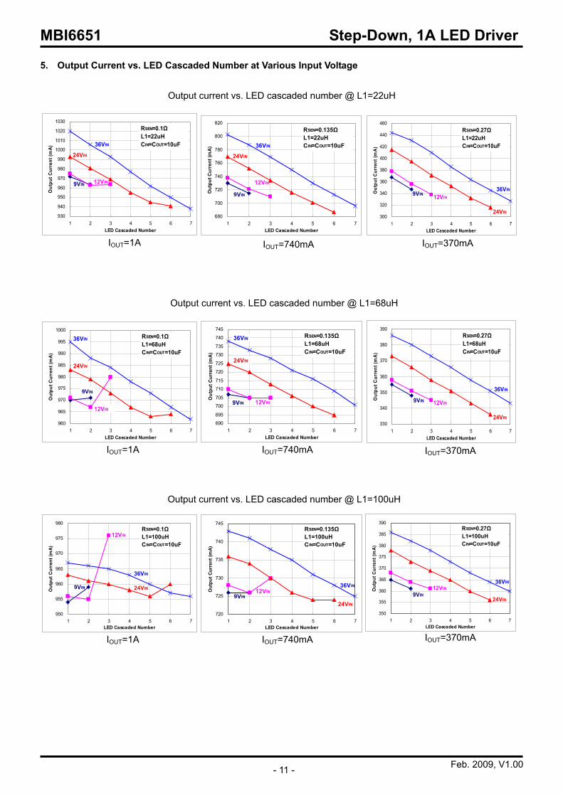
5. Output Current vs. LED Cascaded Number at Various Input Voltage
Output current vs. LED cascaded number @ L1=22uH
930
940
950
960
970
980
990
1000
1010
1020
1030
1 2 3 4 5 6 7LED Cascaded Number
Out
put C
urre
nt (m
A)
RSEN=0.1ΩL1=22uHCIN=COUT=10uF
12VIN
24VIN
36VIN
9VIN
680
700
720
740
760
780
800
820
1 2 3 4 5 6 7LED Cascaded Number
Out
put C
urre
nt (m
A)
RSEN=0.135ΩL1=22uHCIN=COUT=10uF
12VIN
24VIN
36VIN
9VIN
Output current vs. LED cascaded number @ L1=68uH
960
965
970
975
980
985
990
995
1000
1 2 3 4 5 6 7LED Cascaded Number
Out
put C
urre
nt (m
A)
RSEN=0.1ΩL1=68uHCIN=COUT=10uF
12VIN
24VIN
36VIN
9VIN
690
695
700
705
710
715
720
725
730
735
740
745
1 2 3 4 5 6 7LED Cascaded Number
Out
put C
urre
nt (m
A)
RSEN=0.135ΩL1=68uHCIN=COUT=10uF
12VIN
24VIN
36VIN
9VIN
IOUT=1A IOUT=740mA
Output current vs. LED cascaded number @ L1=100uH
950
955
960
965
970
975
980
1 2 3 4 5 6 7LED Cascaded Number
Out
put C
urre
nt (m
A)
RSEN=0.1ΩL1=100uHCIN=COUT=10uF
12VIN
24VIN
36VIN
9VIN
720
725
730
735
740
745
1 2 3 4 5 6 7LED Cascaded Number
Out
put C
urre
nt (m
A)
RSEN=0.135ΩL1=100uHCIN=COUT=10uF
12VIN
24VIN
36VIN
9VIN
IOUT=1A IOUT=740mA
300
320
340
360
380
400
420
440
460
1 2 3 4 5 6 7LED Cascaded Number
Out
put C
urre
nt (m
A)
RSEN=0.27ΩL1=22uHCIN=COUT=10uF
12VIN
24VIN
36VIN9VIN
IOUT=370mA
330
340
350
360
370
380
390
1 2 3 4 5 6 7LED Cascaded Number
Out
put C
urre
nt (m
A)
RSEN=0.27ΩL1=68uHCIN=COUT=10uF
12VIN
24VIN
36VIN
9VIN
IOUT=370mA
350
355
360
365
370
375
380
385
390
1 2 3 4 5 6 7LED Cascaded Number
Out
put C
urre
nt (m
A)
RSEN=0.27ΩL1=100uHCIN=COUT=10uF
12VIN
24VIN
36VIN
9VIN
IOUT=370mA
IOUT=1A IOUT=740mA
MBI6651 Step-Down, 1A LED Driver
Feb. 2009, V1.00 - 12 -
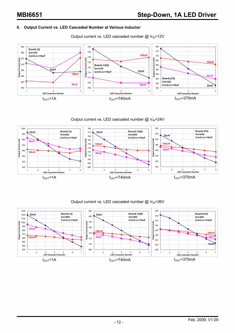
6. Output Current vs. LED Cascaded Number at Various Inductor
Output current vs. LED cascaded number @ VIN=12V
950
955
960
965
970
975
980
985
1 2 3LED Cascaded Number
Out
put C
urre
nt (m
A)
22uH
68uH
100uH
RSEN=0.1ΩVIN=12VCIN=COUT=10uF
700
705
710
715
720
725
730
735
740
1 2 3LED Cascaded Number
Out
put C
urre
nt (m
A)
22uH
68uH
100uH
RSEN=0.135ΩVIN=12VCIN=COUT=10uF
IOUT=1A IOUT=740mA
Output current vs. LED cascaded number @ VIN=24V
930
940
950
960
970
980
990
1000
1 2 3 4 5 6LED Cascaded Number
Out
put C
urre
nt (m
A)
22uH
68uH
100uH
RSEN=0.1ΩVIN=24VCIN=COUT=10uF
680
690
700
710
720
730
740
750
760
770
780
1 2 3 4 5 6LED Cascaded Number
Out
put C
urre
nt (m
A)
22uH
68uH
100uH
RSEN=0.135ΩVIN=24VCIN=COUT=10uF
IOUT=1A IOUT=740mA
Output current vs. LED cascaded number @ VIN=36V
930
940
950
960
970
980
990
1000
1010
1020
1030
1 2 3 4 5 6 7LED Cascaded Number
Out
put C
urre
nt (m
A)
22uH
68uH
100uH
RSEN=0.1ΩVIN=36VCIN=COUT=10uF
680
700
720
740
760
780
800
820
1 2 3 4 5 6 7LED Cascaded Number
Out
put C
urre
nt (m
A)
22uH
68uH
100uH
RSEN=0.135ΩVIN=36VCIN=COUT=10uF
IOUT=1A IOUT=740mA
300
320
340
360
380
400
420
440
460
1 2 3 4 5 6 7LED Cascaded Number
Out
put C
urre
nt (m
A)
22uH
68uH100uH
RSEN=0.27ΩVIN=36VCIN=COUT=10uF
335
340
345
350
355
360
365
370
375
380
1 2 3LED Cascaded Number
Out
put C
urre
nt (m
A)
22uH
68uH
100uH
RSEN=0.27ΩVIN=12VCIN=COUT=10uF
IOUT=370mA
IOUT=370mA
IOUT=370mA
300
320
340
360
380
400
420
440
1 2 3 4 5 6LED Cascaded Number
Out
put C
urre
nt (m
A)
22uH
68uH
100uH
RSEN=0.27ΩVIN=24VCIN=COUT=10uF
MBI6651 Step-Down, 1A LED Driver
Feb. 2009, V1.00 - 13 -
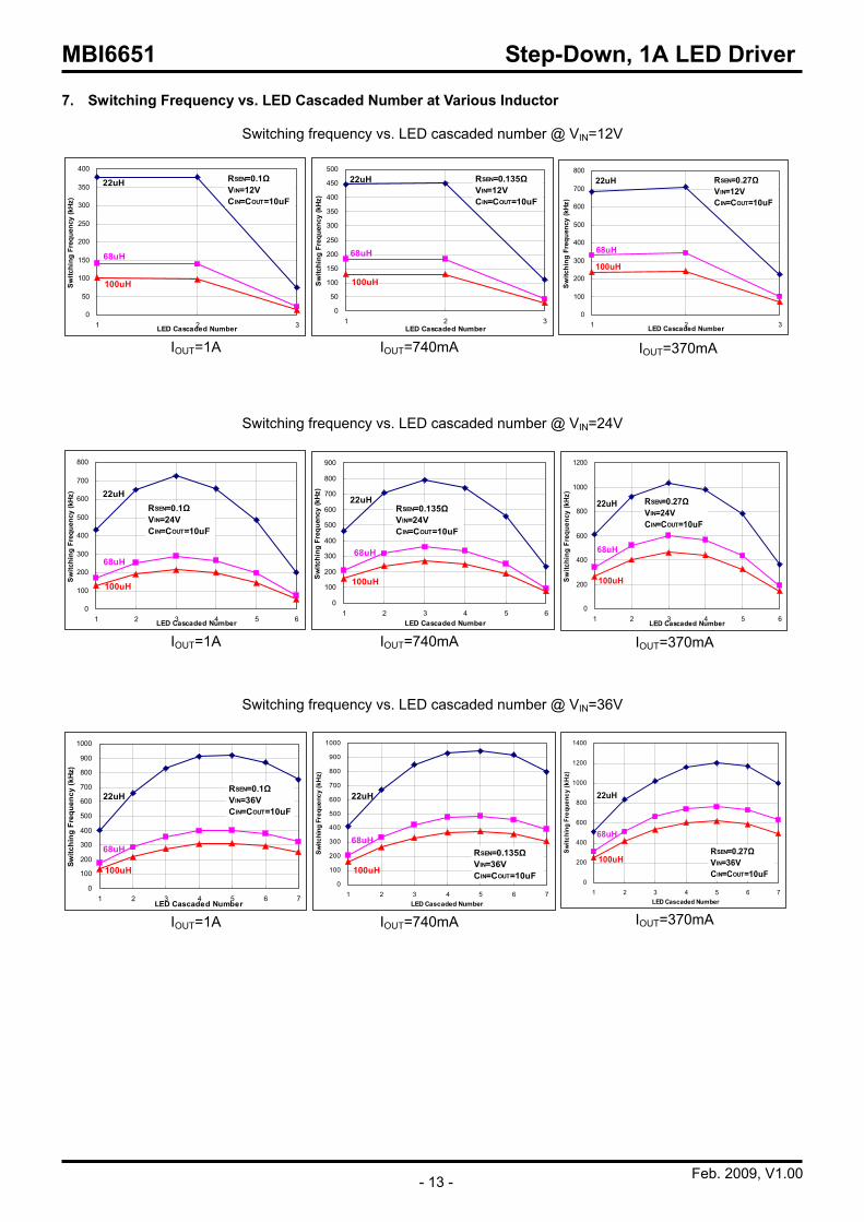
7. Switching Frequency vs. LED Cascaded Number at Various Inductor
Switching frequency vs. LED cascaded number @ VIN=12V
0
50
100
150
200
250
300
350
400
1 2 3LED Cascaded Number
Switc
hing
Fre
quen
cy (k
Hz)
RSEN=0.1ΩVIN=12VCIN=COUT=10uF
22uH
68uH
100uH
0
50
100
150
200
250
300
350
400
450
500
1 2 3LED Cascaded Number
Sw
itchi
ng F
requ
ency
(kHz
)
RSEN=0.135ΩVIN=12VCIN=COUT=10uF
22uH
68uH
100uH
IOUT=1A IOUT=740mA
Switching frequency vs. LED cascaded number @ VIN=24V
0
100
200
300
400
500
600
700
800
1 2 3 4 5 6LED Cascaded Number
Switc
hing
Fre
quen
cy (k
Hz)
RSEN=0.1ΩVIN=24VCIN=COUT=10uF
22uH
68uH
100uH
0
100
200
300
400
500
600
700
800
900
1 2 3 4 5 6LED Cascaded Number
Sw
itchi
ng F
requ
ency
(kHz
)
RSEN=0.135ΩVIN=24VCIN=COUT=10uF
22uH
68uH
100uH
IOUT=1A IOUT=740mA
Switching frequency vs. LED cascaded number @ VIN=36V
0
100
200
300
400
500
600
700
800
900
1000
1 2 3 4 5 6 7LED Cascaded Number
Switc
hing
Fre
quen
cy (k
Hz)
RSEN=0.1ΩVIN=36VCIN=COUT=10uF
22uH
68uH
100uH0
100
200
300
400
500
600
700
800
900
1000
1 2 3 4 5 6 7LED Cascaded Number
Switc
hing
Fre
quen
cy (k
Hz)
22uH
68uH
100uH
RSEN=0.135ΩVIN=36VCIN=COUT=10uF
IOUT=1A IOUT=740mA
0
200
400
600
800
1000
1200
1 2 3 4 5 6LED Cascaded Number
Sw
itchi
ng F
requ
ency
(kH
z)
RSEN=0.27ΩVIN=24VCIN=COUT=10uF
22uH
68uH
100uH
0
100
200
300
400
500
600
700
800
1 2 3LED Cascaded Number
Switc
hing
Fre
quen
cy (k
Hz)
RSEN=0.27ΩVIN=12VCIN=COUT=10uF
22uH
68uH
100uH
IOUT=370mA
IOUT=370mA
0
200
400
600
800
1000
1200
1400
1 2 3 4 5 6 7LED Cascaded Number
Switc
hing
Fre
quen
cy (k
Hz)
22uH
68uH
100uHRSEN=0.27ΩVIN=36VCIN=COUT=10uF
IOUT=370mA
MBI6651 Step-Down, 1A LED Driver
Feb. 2009, V1.00 - 14 -
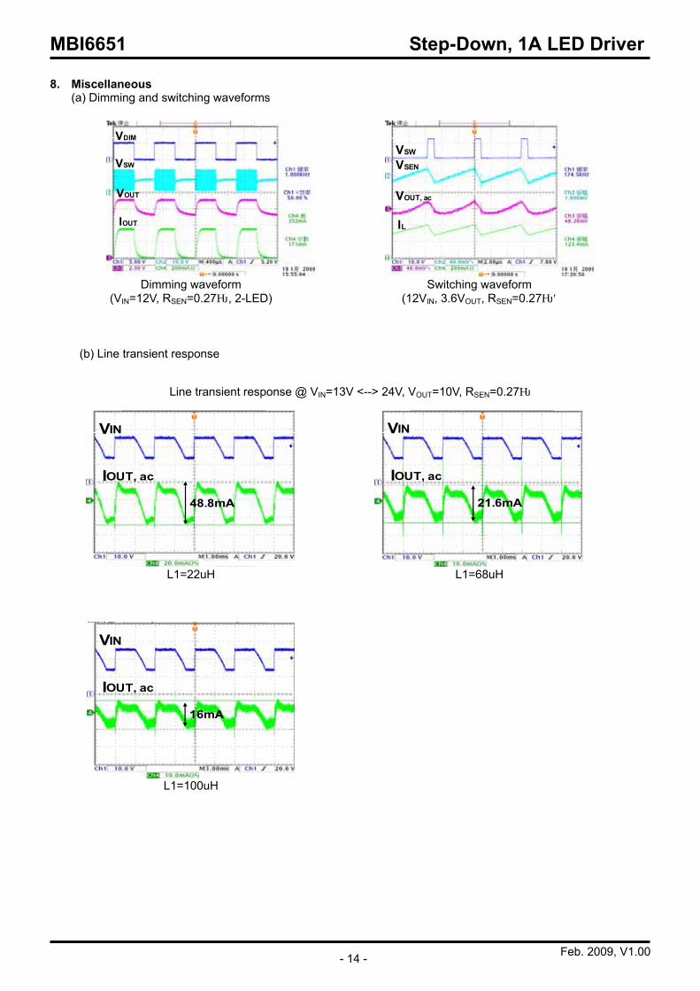
8. Miscellaneous
(a) Dimming and switching waveforms
VDIM
VSW
VOUT
IOUT
VSEN
VSW
VOUT, ac
IL
Dimming waveform Switching waveform (VIN=12V, RSEN=0.27Ω, 2-LED) (12VIN, 3.6VOUT, RSEN=0.27Ω)
(b) Line transient response
Line transient response @ VIN=13V <--> 24V, VOUT=10V, RSEN=0.27Ω
VIN
IOUT, ac
48.8mA
VIN
IOUT, ac
21.6mA
L1=22uH L1=68uH
VIN
IOUT, ac
16mA
L1=100uH
MBI6651 Step-Down, 1A LED Driver
Feb. 2009, V1.00 - 15 -
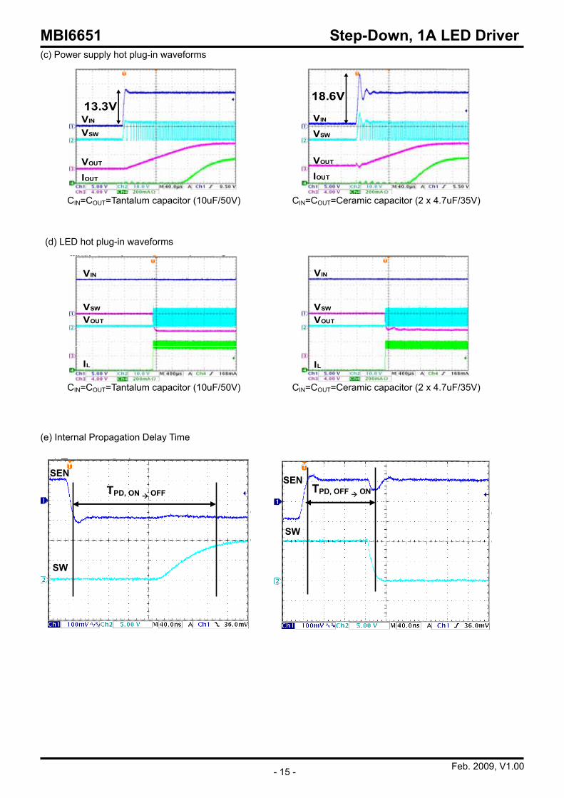
(c) Power supply hot plug-in waveforms
VIN
VSW
VOUT
IOUT
13.3V
VIN
VSW
VOUT
IOUT
18.6V
CIN=COUT=Tantalum capacitor (10uF/50V) CIN=COUT=Ceramic capacitor (2 x 4.7uF/35V)
(d) LED hot plug-in waveforms
VIN
VSW
VOUT
IL
VIN
VSW
VOUT
IL
CIN=COUT=Tantalum capacitor (10uF/50V) CIN=COUT=Ceramic capacitor (2 x 4.7uF/35V)
(e) Internal Propagation Delay Time
SEN
SW
TPD, ON OFF SEN
SW
TPD, OFF ON
MBI6651 Step-Down, 1A LED Driver
Feb. 2009, V1.00 - 16 -
VIN
VSW
VOUT
IOUT404mA 350mA
Application Information
The MBI6651 is a simple and high efficient buck converter with capability to drive up to 1A of loading. The MBI6651
adopts hysteretic PFM control scheme to regulate loading and input voltage variations. The hysteretic PFM control
requires no loop compensation bringing very fast load transient response and achieving excellent efficiency at light
loading.
Setting Output Current The output current (IOUT) is set by an external resistor, RSEN. The relationship between IOUT and RSEN is as below;
VSEN=0.1V;
RSEN=(VSEN/IOUT)=(0.1V/IOUT);
IOUT=(VSEN/RSEN)=(0.1V/RSEN) where RSEN is the resistance of the external resistor connecting to SEN terminal and VSEN is the voltage of external
resistor. The magnitude of current (as a function of RSEN) is around 1000mA at 0.1Ω.
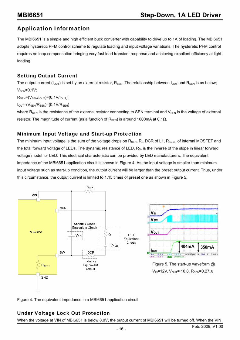
Minimum Input Voltage and Start-up Protection The minimum input voltage is the sum of the voltage drops on RSEN, RS, DCR of L1, Rds(on) of internal MOSFET and
the total forward voltage of LEDs. The dynamic resistance of LED, RS, is the inverse of the slope in linear forward
voltage model for LED. This electrical characteristic can be provided by LED manufacturers. The equivalent
impedance of the MBI6651 application circuit is shown in Figure 4. As the input voltage is smaller than minimum
input voltage such as start-up condition, the output current will be larger than the preset output current. Thus, under
this circumstance, the output current is limited to 1.15 times of preset one as shown in Figure 5.
Figure 4. The equivalent impedance in a MBI6651 application circuit Under Voltage Lock Out Protection When the voltage at VIN of MBI6651 is below 8.0V, the output current of MBI6651 will be turned off. When the VIN
Figure 5. The start-up waveform @
VIN=12V, VOUT= 10.8, RSEN=0.27Ω
MBI6651 Step-Down, 1A LED Driver
Feb. 2009, V1.00 - 17 -
VSW
VOUT
IIN
IL
voltage of MBI6651 resumes to 8.0V, the output current of MBI6651 will be turned on again.
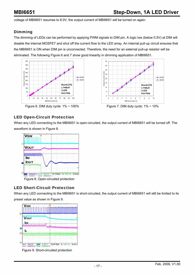
Dimming The dimming of LEDs can be performed by applying PWM signals to DIM pin. A logic low (below 0.5V) at DIM will
disable the internal MOSFET and shut off the current flow to the LED array. An internal pull-up circuit ensures that
the MBI6651 is ON when DIM pin is unconnected. Therefore, the need for an external pull-up resistor will be
eliminated. The following Figure 6 and 7 show good linearity in dimming application of MBI6651.
0
50
100
150
200
250
300
350
400
450
0 10 20 30 40 50 60 70 80 90 100
DIM Duty Cycle (%)
Out
put C
urre
nt (m
A)
24VIN36VIN
RSEN=0.27ΩL1=68uH3-LEDfDIM=1kHz
0
5
10
15
20
25
30
35
40
0 1 2 3 4 5 6 7 8 9 10
DIM Duty Cycle (%)
Out
put C
urre
nt (m
A)
24VIN36VIN
RSEN=0.27ΩL1=68uH3-LEDfDIM=1kHz
Figure 6. DIM duty cycle: 1% ~ 100% Figure 7. DIM duty cycle: 1% ~ 10%
LED Open-Circuit Protection When any LED connecting to the MBI6651 is open-circuited, the output current of MBI6651 will be turned off. The
waveform is shown in Figure 8.
VSW
VOUT
IINIOUT
LED Short-Circuit Protection When any LED connecting to the MBI6651 is short-circuited, the output current of MBI6651 will still be limited to its
preset value as shown in Figure 9.
Figure 9. Short-circuited protection
Figure 8. Open-circuited protection
MBI6651 Step-Down, 1A LED Driver
Feb. 2009, V1.00 - 18 -
VIN
VSW
VOUT
IOUT
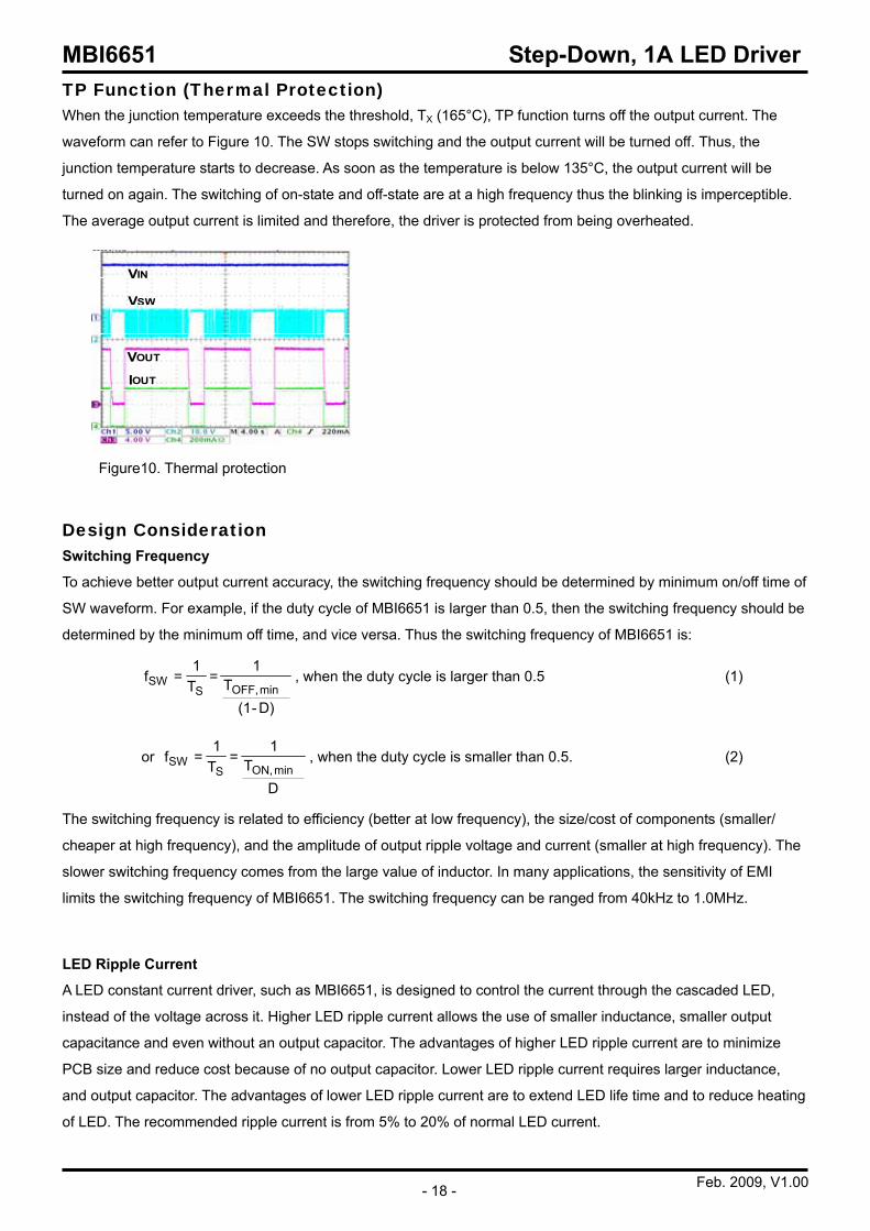
TP Function (Thermal Protection) When the junction temperature exceeds the threshold, TX (165°C), TP function turns off the output current. The
waveform can refer to Figure 10. The SW stops switching and the output current will be turned off. Thus, the
junction temperature starts to decrease. As soon as the temperature is below 135°C, the output current will be
turned on again. The switching of on-state and off-state are at a high frequency thus the blinking is imperceptible.
The average output current is limited and therefore, the driver is protected from being overheated.
Figure10. Thermal protection
Design Consideration Switching Frequency
To achieve better output current accuracy, the switching frequency should be determined by minimum on/off time of
SW waveform. For example, if the duty cycle of MBI6651 is larger than 0.5, then the switching frequency should be
determined by the minimum off time, and vice versa. Thus the switching frequency of MBI6651 is:
D)-(1 T
1 =
T1
=fmin OFF,S
SW , when the duty cycle is larger than 0.5 (1)
or
D T
1 =
T1
=fmin ON,S
SW , when the duty cycle is smaller than 0.5. (2)
The switching frequency is related to efficiency (better at low frequency), the size/cost of components (smaller/
cheaper at high frequency), and the amplitude of output ripple voltage and current (smaller at high frequency). The
slower switching frequency comes from the large value of inductor. In many applications, the sensitivity of EMI
limits the switching frequency of MBI6651. The switching frequency can be ranged from 40kHz to 1.0MHz.
LED Ripple Current
A LED constant current driver, such as MBI6651, is designed to control the current through the cascaded LED,
instead of the voltage across it. Higher LED ripple current allows the use of smaller inductance, smaller output
capacitance and even without an output capacitor. The advantages of higher LED ripple current are to minimize
PCB size and reduce cost because of no output capacitor. Lower LED ripple current requires larger inductance,
and output capacitor. The advantages of lower LED ripple current are to extend LED life time and to reduce heating
of LED. The recommended ripple current is from 5% to 20% of normal LED current.
MBI6651 Step-Down, 1A LED Driver
Feb. 2009, V1.00 - 19 -
Component Selection Inductor Selection
The inductance is determined by two factors: the switching frequency and the inductor ripple current. The
calculation of the inductance, L1, can be described as
LSWOUTds(on)SENOUTIN I∆ x f
D x ))I x (R - V- V- V( > L1
where Rds(on) is the on-resistance of internal MOSFET of the MBI6651. The typical is 0.45Ω at 12VIN. D is the duty cycle of the MBI6651, D=VOUT/VIN.
fSW is the switching frequency of the MBI6651.
IL is the ripple current of inductor, IL=(1.15xIOUT)–(0.85xIOUT)=0.3xIOUT.
When selecting an inductor, not only the inductance but also the saturation current that should be considered as
the factors to affect the performance of module. In general, it is recommended to choose an inductor with 1.5 times
of LED current as the saturation current. Also, the larger inductance gains the better line/load regulation. However,
the inductance and saturation current become a trade-off at the same inductor size. An inductor with shield is
recommended to reduce the EMI interference, however, this is another trade-off with heat dissipation.
Schottky Diode Selection The MBI6651 needs a flywheel diode, D1, to carry the inductor current when the MOSFET is off. The
recommended flywheel diode is schottky diode with low forward voltage for better efficiency. Two factors determine
the selection of schottky diode. One is the maximum reverse voltage. The recommended rated voltage of the
reverse voltage is at least 1.5 times of input voltage. The other is the maximum forward current, which works when
the MOSFET is off. And the recommended forward current is 1.5 times of output current. Users should carefully
choose an appropriate schottky diode which can perform low leakage current at high temperature.
Input Capacitor Selection
The input capacitor, CIN, can supply pulses of current for the MBI6651 when the MOSFET is ON. And CIN is
charged by input voltage when the MOSFET is OFF. As the input voltage is lower than the tolerable input voltage,
the internal MOSFET of the MBI6651 remains constantly ON, and the LED current is limited to 1.15 times of normal
current. The recommended value of input capacitor is 10uF to stabilize the lighting system.
The rated voltage of input capacitor should be at least 1.5 times of input voltage. A tantalum or ceramic capacitor
can be used as an input capacitor. The advantages of tantalum capacitor are high capacitance and low ESR. The
advantages of ceramic capacitor are high frequency characteristic, small size and low cost. Due to low ESR
characteristic of ceramic capacitor, please do not use hot plugging. Users can choose an appropriate one for their
applications.
Output Capacitor Selection (Optional)
A capacitor paralleled with cascaded LED can reduce the LED ripple current and allow smaller inductance.
MBI6651 Step-Down, 1A LED Driver
Feb. 2009, V1.00 - 20 -
PCB Layout Consideration To enhance the efficiency and stabilize the system, careful considerations of PCB layout is important. There are
several factors should be considered.
1. A complete ground area is helpful to eliminate the switching noise.
2. Keep the IC’s GND pin and the ground leads of input and output filter capacitors less than 5mm.
3. To maximize output power efficiency and minimize output ripple voltage, use a ground plane and solder the IC’s
GND pin directly to the ground plane.
4. To stabilize the system, the heat sink of the MBI6651 is recommended to connect to ground plane directly.
5. Enhance the heat dissipation, the area of ground plane, which IC’s heat sink is soldered on, should be as large
as possible.
6. The input capacitor should be placed to IC’s VIN pin as close as possible.
7. To avoid the parasitic effect of trace, the RSEN should be placed to IC’s VIN and SEN pins as close as possible.
8. The area, which is composed of IC’s SW pin, schottky diode and inductor, should be wide and short.
9. The path, which flows large current, should be wide and short to eliminate the parasite element.
10. When SW is ON/OFF, the direction of power loop should keep the same way to enhance the efficiency. The
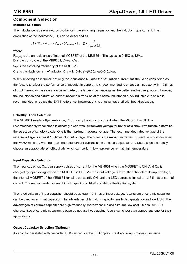
sketch is shown as Figure11.
+-
+ C
R
LED1 LEDn
L1
SW
D1
SW --> ON
SW --> OFF
IN
VIN
SEN
Figure 11. Power loop of MBI6651
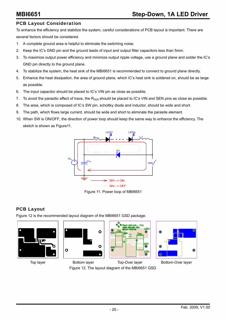
PCB Layout Figure 12 is the recommended layout diagram of the MBI6651 GSD package.
Top layer Bottom layer Top-Over layer Bottom-Over layer Figure 12. The layout diagram of the MBI6651 GSD
MBI6651 Step-Down, 1A LED Driver
Feb. 2009, V1.00 - 21 -
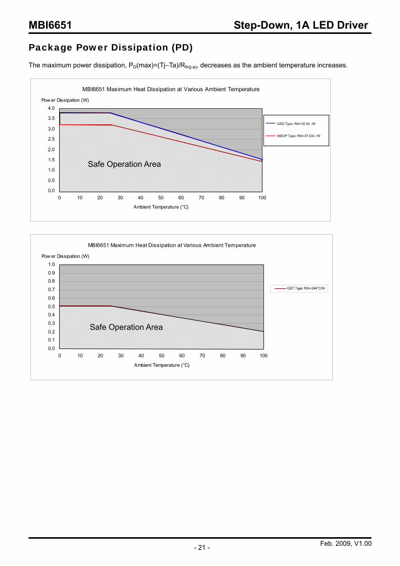
Package Power Dissipation (PD)
The maximum power dissipation, PD(max)=(Tj–Ta)/Rth(j-a), decreases as the ambient temperature increases.
MBI6651 Maximum Heat Dissipation at Various Ambient Temperature
0.0
0.5
1.0
1.5
2.0
2.5
3.0
3.5
4.0
0 10 20 30 40 50 60 70 80 90 100
Ambient Temperature (°C)
Pow er Dissipation (W)
GSD Type: Rth=32.9°C/W
MBI6651 Maximum Heat Dissipation at Various Ambient Temperature
0.0
0.10.2
0.3
0.40.5
0.6
0.7
0.80.9
1.0
0 10 20 30 40 50 60 70 80 90 100
Ambient Temperature (°C)
Pow er Dissipation (W)
GST Type: Rth=244°C/W
Safe Operation Area
Safe Operation Area
GSD Type: Rth=32.9/W
MSOP Type: Rth=37.53/W
MBI6651 Step-Down, 1A LED Driver
Feb. 2009, V1.00 - 22 -
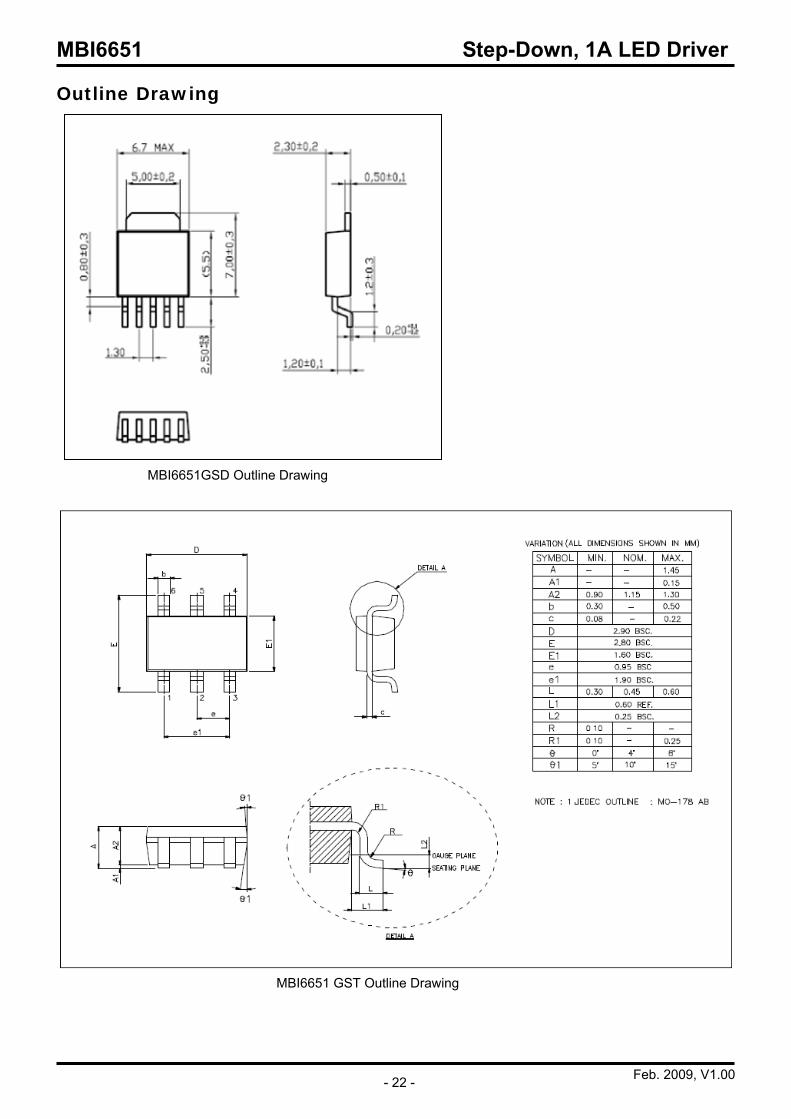
MBI6651GSD Outline Drawing
MBI6651 GST Outline Drawing
Outline Drawing
MBI6651 Step-Down, 1A LED Driver
Feb. 2009, V1.00 - 23 -
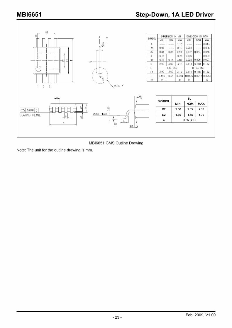
MBI6651 GMS Outline Drawing
Note: The unit for the outline drawing is mm.
0.65 BSCe
1.701.651.60E2
2.102.052.00D2
MAX.NOM.MIN.
8LSYMBOL
0.65 BSCe
1.701.651.60E2
2.102.052.00D2
MAX.NOM.MIN.
8LSYMBOL
MBI6651 Step-Down, 1A LED Driver
Feb. 2009, V1.00 - 24 -
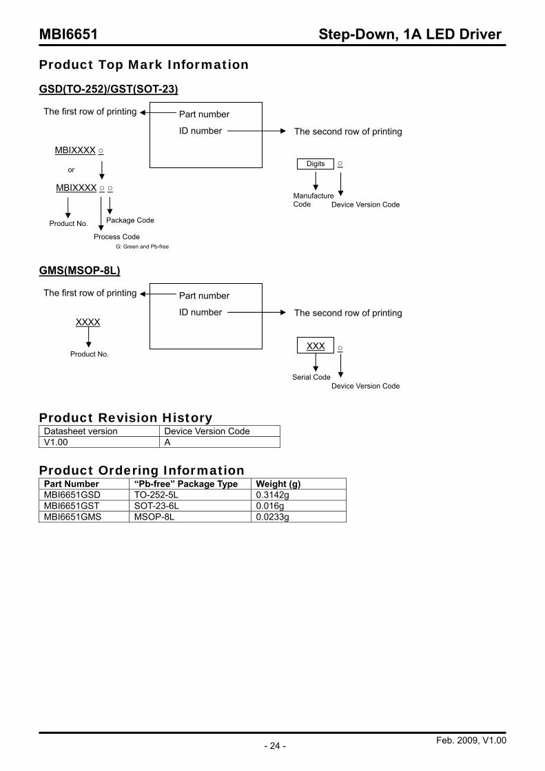
Product Top Mark Information
GSD(TO-252)/GST(SOT-23)
GMS(MSOP-8L)
Product Revision History Datasheet version Device Version Code V1.00 A
Product Ordering Information Part Number “Pb-free” Package Type Weight (g) MBI6651GSD TO-252-5L 0.3142g MBI6651GST SOT-23-6L 0.016g MBI6651GMS MSOP-8L 0.0233g
Process Code G: Green and Pb-free
Part number
ID number
ManufactureCode Device Version Code
The second row of printing
The first row of printing
Product No. Package Code
MBIXXXX
Digits
MBIXXXX
or
Part number
ID number
Serial Code Device Version Code
The second row of printing
The first row of printing
Product No. XXX
XXXX

MBI6651 Step-Down, 1A LED Driver
Feb. 2009, V1.00 - 25 -
Disclaimer
Macroblock reserves the right to make changes, corrections, modifications, and improvements to their products and
documents or discontinue any product or service without notice. Customers are advised to consult their sales
representative for the latest product information before ordering. All products are sold subject to the terms and
conditions supplied at the time of order acknowledgement, including those pertaining to warranty, patent
infringement, and limitation of liability. Macroblock’s products are not designed to be used as components in device intended to support or sustain life or
in military applications. Use of Macroblock’s products in components intended for surgical implant into the body, or
other applications in which failure of Macroblock’s products could create a situation where personal death or injury
may occur, is not authorized without the express written approval of the Managing Director of Macroblock.
Macroblock will not be held liable for any damages or claims resulting from the use of its products in medical and
military applications. All text, images, logos and information contained on this document is the intellectual property of Macroblock.
Unauthorized reproduction, duplication, extraction, use or disclosure of the above mentioned intellectual property
will be deemed as infringement.