Embed Size (px)
Citation preview
MC92602 Reduced Interface SerDes Design Verification Board
User’s Guide
MC92602DVBUG Rev. 3, 06/2005

MC92602 Reduced Interface SerDes Design Verification Board User’s Guide, Rev. 3
Freescale Semiconductor iii
Contents
Paragraph Page Number Title Number
Chapter 1 General Information
1.1 Introduction...................................................................................................................... 1-11.2 Design Verification Board Features ................................................................................. 1-11.3 Specifications................................................................................................................... 1-21.4 Abbreviation List ............................................................................................................. 1-21.5 Related Documentation.................................................................................................... 1-31.6 Block Diagram................................................................................................................. 1-31.7 Board Components .......................................................................................................... 1-31.8 Contact Information......................................................................................................... 1-3
Chapter 2 Hardware Preparation and Installation
2.1 Unpacking Instructions .................................................................................................... 2-12.2 MC92602DVB Package Contents ................................................................................... 2-12.3 Hardware Preparation ...................................................................................................... 2-12.3.1 Setting the Power Supply and Voltage Regulators ...................................................... 2-12.3.2 Setting the Voltage Regulators..................................................................................... 2-22.3.3 HSTL Voltage Reference Regulator ............................................................................ 2-32.4 Reference Clock Source................................................................................................... 2-32.4.1 Using the Onboard Oscillator ...................................................................................... 2-42.4.2 External Reference Clock Source ................................................................................ 2-42.4.3 Supplying a Clock to the MC92602 ............................................................................ 2-42.4.4 3.3V_CLK_OUTn SMA Connectors .......................................................................... 2-52.4.5 Clock Frequency Selection .......................................................................................... 2-52.5 Interface Components ...................................................................................................... 2-62.5.1 Parallel Inputs and Outputs.......................................................................................... 2-62.5.1.1 Parallel Inputs .......................................................................................................... 2-62.5.1.2 Parallel Outputs ....................................................................................................... 2-72.5.2 +VDDQ and Ground (GND) Access Connections........................................................ 2-72.5.3 Serial Inputs and Outputs............................................................................................. 2-72.6 Special Test Connection................................................................................................... 2-72.7 Test Traces ....................................................................................................................... 2-8
MC92602 Reduced Interface SerDes Design Verification Board User’s Guide, Rev. 3
iv Freescale Semiconductor
Paragraph Page Number Title Number
Chapter 3
Laboratory Equipment and Quick Setup Evaluation
3.1 Recommended Laboratory Equipment ............................................................................ 3-13.2 Quick Setup Data-Eye Diagram ...................................................................................... 3-23.2.1 Quick Setup Data-Eye Generation and Observation ................................................... 3-33.2.1.1 Equipment Setup...................................................................................................... 3-33.2.1.2 Parallel Input Connections....................................................................................... 3-43.2.2 Basic Eye ObservationTest Procedure..................................................................... 3-53.2.3 Quick Setup Bit Error Rate Checking.......................................................................... 3-63.2.3.1 Equipment Setup...................................................................................................... 3-63.2.3.2 Parallel I/O Connections.......................................................................................... 3-73.2.3.3 Quick Setup BERC Test Procedure ......................................................................... 3-7
Chapter 4 Test Setups
4.1 Serial Link Verification Using a Serial Bit Error Rate Tester (BERT) ............................ 4-14.1.1 Test Setup for Full-Speed Mode .................................................................................. 4-24.1.2 Test Setup for Half-Speed Mode ................................................................................. 4-24.2 Jitter Testing..................................................................................................................... 4-34.2.1 Jitter Test System Calibration ...................................................................................... 4-34.2.2 Reference Clock Jitter Transfer Test............................................................................ 4-44.2.3 Reference Clock Jitter Tolerance Test ......................................................................... 4-54.2.4 Data Jitter Tolerance Test............................................................................................. 4-6
Appendix A Connector Signals
A.1 Input: 2 × 10 (0.100") Connectors.................................................................................... A-1A.1.1 Control Signal Input Connectors ................................................................................ A-1A.1.2 Transmitter Parallel Data Input Connectors ............................................................... A-3A.2 Output: 2 × 20 (0.100") Connectors................................................................................. A-4A.3 TEST_0 Connector ......................................................................................................... A-5
Appendix B Parts List
B.1 Design Verification Board Parts List ...............................................................................B-1
MC92602 Reduced Interface SerDes Design Verification Board User’s Guide, Rev. 3
Freescale Semiconductor v
Paragraph Page Number Title Number
Appendix C Prescaler for Jitter Measurement
C.1 Divide-by-xx Prescaler Description .................................................................................C-1C.2 Prescaler Components......................................................................................................C-2
Appendix D Revision History

MC92602 Reduced Interface SerDes Design Verification Board User’s Guide, Rev. 3
vi Freescale Semiconductor
MC92602 Reduced Interface SerDes Design Verification Board User’s Guide, Rev. 3
Freescale Semiconductor 1-1
Chapter 1 General Information
1.1 Introduction
This users guide describes the MC92602 design verification board, Rev. B and higher. The design verification board (DVB) facilitates the full evaluation of the MC92602 Quad Reduced Interface SerDes. It should be read in conjunction with the MC92602 Quad 1.25 Gbaud Reduced Interface SerDes Reference Guide. This design verification board is intended for evaluation and testing purposes only. Freescale does not guarantee its performance in a production environment.
This board was designed to be used with laboratory equipment (pattern generators, data analyzers, BERT, scopes, etc.) or connected to other evaluation boards. Access to the MC92602 device (verification chip) is through connectors to each pin, to allow complete in-depth design verification testing of the chip design. This allows the user to check any or all features/functions of the MC92602 device.
The four parallel data input ports and all configuration/control signal pins, are accessed through common 2 × 10, 0.100" male connectors (headers). The parallel data output ports are accessed through 2 × 20, 0.100" connectors. Device JTAG port signals are also accessed with a separate connector.
The MC92602 high-speed serial receivers and transmitters are accessed via SMA coaxial connectors for signal integrity measurements.
A single 5.0-V power source is required for the DVB operation. All necessary voltages are generated by regulators onboard. The reference clock for the MC92602 chip may be provided using either an external clock or the onboard crystal oscillator. Clock drivers on the DVB provide additional clock signals for triggering analyzer instrumentation and scopes.
1.2 Design Verification Board FeaturesThe functional, physical, and performance features of the MC92602DVB are as follows:
A single external 5.0-V to onboard regulators supply power to all onboard circuitry. Reference clock source is a 250-MHz crystal oscillator or an external clock source. Parallel data and control interfaces accessible through standard 0.100", 2 row connectors for data
generators and analyzers. The full-duplex differential data links accessible through SMA connectors. Two pairs of 50-Ω test traces with SMA connections facilitate TDR measurements of the
characteristic impedance of representative board traces. Connector provided for JTAG test access port
General Information
MC92602 Reduced Interface SerDes Design Verification Board User’s Guide, Rev. 3
1-2 Freescale Semiconductor
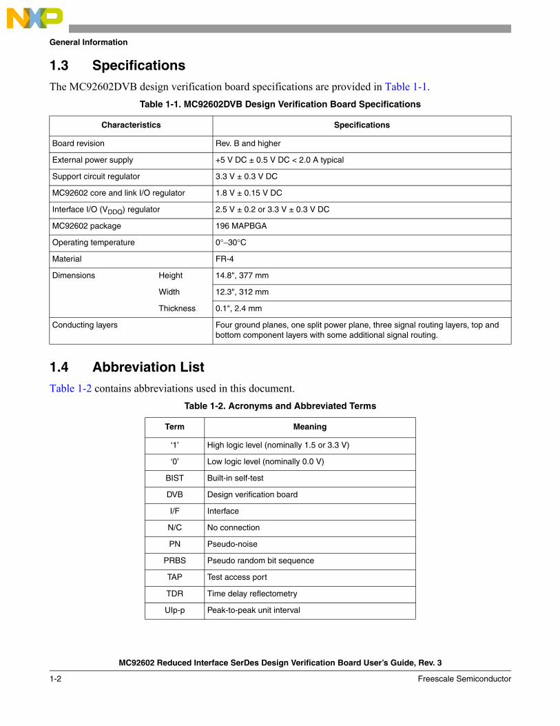
1.3 SpecificationsThe MC92602DVB design verification board specifications are provided in Table 1-1.
1.4 Abbreviation ListTable 1-2 contains abbreviations used in this document.
Table 1-1. MC92602DVB Design Verification Board Specifications
Characteristics Specifications
Board revision Rev. B and higher
External power supply +5 V DC ± 0.5 V DC < 2.0 A typical
Support circuit regulator 3.3 V ± 0.3 V DC
MC92602 core and link I/O regulator 1.8 V ± 0.15 V DC
Interface I/O (VDDQ) regulator 2.5 V ± 0.2 or 3.3 V ± 0.3 V DC
MC92602 package 196 MAPBGA
Operating temperature 0°−30°C
Material FR-4
Dimensions Height 14.8", 377 mm
Width 12.3", 312 mm
Thickness 0.1", 2.4 mm
Conducting layers Four ground planes, one split power plane, three signal routing layers, top and bottom component layers with some additional signal routing.
Table 1-2. Acronyms and Abbreviated Terms
Term Meaning
‘1’ High logic level (nominally 1.5 or 3.3 V)
‘0’ Low logic level (nominally 0.0 V)
BIST Built-in self-test
DVB Design verification board
I/F Interface
N/C No connection
PN Pseudo-noise
PRBS Pseudo random bit sequence
TAP Test access port
TDR Time delay reflectometry
UIp-p Peak-to-peak unit interval
General Information
MC92602 Reduced Interface SerDes Design Verification Board User’s Guide, Rev. 3
Freescale Semiconductor 1-3
1.5 Related DocumentationRelated documentation includes the following:
MC92602 Quad 1.25 Gbaud Reduced Interface SerDes Reference Guide (MC92602RM) MC92602DVB schematics MC100ES6222 data sheet MC100ES8111 data sheet MPC9456 data sheet
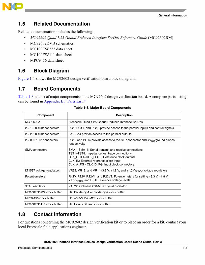
1.6 Block DiagramFigure 1-1 shows the MC92602 design verification board block diagram.
1.7 Board ComponentsTable 1-3 is a list of major components of the MC92602 design verification board. A complete parts listing can be found in Appendix B, Parts List.
1.8 Contact InformationFor questions concerning the MC92602 design verification kit or to place an order for a kit, contact your local Freescale field applications engineer.
Table 1-3. Major Board Components
Component Description
MC92602ZT Freescale Quad 1.25 Gbaud Reduced Interface SerDes
2 × 10, 0.100" connectors PG1–PG11, and PG13 provide access to the parallel inputs and control signals
2 × 20, 0.100" connectors LA1–LA4 provide access to the parallel outputs
2 × 8, 0.100" connectors PG12 and PG14 provide access to the SFP connector and +VDD/ground planes, respectively.
SMA connectors SMA1–SMA16: Serial transmit and receive connectionsTST1–TST8: Impedance test trace connectionsCLK_OUT1–CLK_OUT6: Reference clock outputsCLK_IN: External reference clock inputCLK_A_PG - CLK_D_PG: Input clock connectors
LT1587 voltage regulators VR33, VR18, and VR1: +3.3 V, +1.8 V, and +1.5 (VDDQ) voltage regulators
Potentiometers R12V, R22V, R22V1, and R22V2: Potentiometers for setting +3.3 V, +1.8 V, +1.5 VDDQ, and HSTL reference voltage levels
XTAL oscillator Y1, Y2: Onboard 250-MHz crystal oscillator
MC100ES6222 clock buffer U2: Divide-by-1 or divide-by-2 clock buffer
MPC9456 clock buffer U3: +3.3-V LVCMOS clock buffer
MC100ES8111 clock buffer U4: Level shift and clock buffer
General Information
MC92602 Reduced Interface SerDes Design Verification Board User’s Guide, Rev. 3
1-4 Freescale Semiconductor
Figure 1-1. MC92602 Design Verification Board Block Diagram
MC92602
2 × 20, 0.100"
RECV_A
2×10, 0.100" Connectors
XMIT_A
+3.3-VRegulator
+1.5-VRegulator
+5 V
MC100MPC9456
Horizontal 50-Ω
Test Traces
Vertical 50-ΩTest Traces
XMIT_B Ctrl/Tst
RECV_B
RECV_C
RECV_D
XMIT_C XMIT_DControl
2×10, 0.100" Connectors
SW1
Connectors
1.5V_CLK_OUT5
1.5V_CLK_OUT6
CLK_IN
RLINK_D0
RLINK_C0
RLINK_B0
RLINK_A0
XLINK_D0
XLINK_C0
XLINK_B0
XLINK_A0
TST1 TST2
TST5 TST6
TST3 TST7TST4 TST8
0.100" Connector
+1.5 V/GND
R22V1
R12V
+3.3 V
TPA
GND
+1.8-VRegulator
R22V
3.3V_CLK_OUT2
3.3V_CLK_OUT3
HSTL_VREF
R22V2
X-TALOsc
CLK_B_PG
CLK_A_PG
CLK_C_PG
CLK_D_PG
ES6222
MC100ES8111
3.3V_CLK_OUT1
HSTL_VREF
LA4
LA3
LA2
LA1
PG1
PG6
PG7 PG4
PG5
+1.5 V
+1.8 V
Reduced InterfaceSerDes
PG10
PG11PG8PG8
PG3
PG13PG2
3.3V_CLK_OUT4
PG9

MC92602 Reduced Interface SerDes Design Verification Board User’s Guide, Rev. 3
Freescale Semiconductor 2-1
Chapter 2 Hardware Preparation and InstallationThis chapter provides unpacking, hardware preparation, configuration-installation instructions, and description of the interface components for the MC92602DVB.
2.1 Unpacking InstructionsUnpack the board from the shipping carton. Refer to the packing list and verify that all items are present. Save the packing material for storing and reshipping of the equipment.
2.2 MC92602DVB Package ContentsTable 2-1 describes the contents of the MC92602DVB kit.
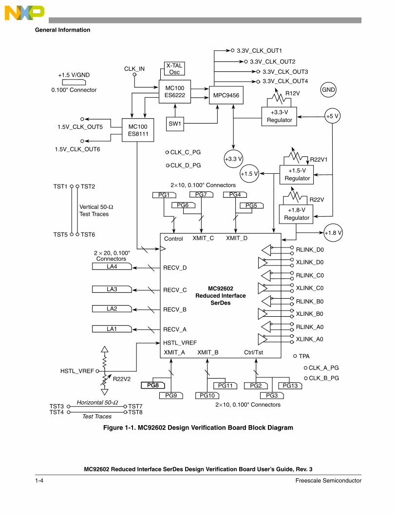
2.3 Hardware PreparationOperation of the MC92602DVB requires proper setup of the power supply and voltage regulators as well as the reference clock. Figure 2-1 depicts the location of the major components on the board. The following sections describe proper setup of the MC92602DVB.
2.3.1 Setting the Power Supply and Voltage Regulators
The MC92602DVB requires a single +5.0-V supply. Fully operational, the board will draw a maximum current less than 2.0 amps from the +5.0-V supply. Actual current consumption depends on the user set voltage levels, clock frequencies, and the MC92602 operating mode. The board contains two +5.0-V connection posts and two ground connection posts. These duplicate connections simplify using a four-wire supply: supply and ground, force and sense.
Table 2-1. MC92602DVB Kit Contents
Quantity Item
1 MC92602DVB design verification board
1 MC92602DVB Reduced Interface SerDes Design Verification Board User’s Guide
1 MC92602 Quad 1.25 Gbaud Reduced Interface SerDes Reference Guide
1 Complete set of MC92602DVB design verification board schematics
45 0.100" shunts
10 Square pin receptacle patch cords
Hardware Preparation and Installation
MC92602 Reduced Interface SerDes Design Verification Board User’s Guide, Rev. 3
2-2 Freescale Semiconductor
Figure 2-1. Top Side Part Location Diagram
2.3.2 Setting the Voltage Regulators
The +5.0-V supply is used to power 3 onboard voltage regulators, VR33, VR18, and VR15. These regulators generate +3.3, +1.8, and +1.5/1.8 V (VDDQ), respectively. The +3.3-V supply provides power to the oscillator and clock buffer chips. This supply can be varied over the range +3.3 V ± 0.3 V using the R12V potentiometer.
The +1.8-V supply is used to power the MC92602 core logic, transceivers, and on-chip phase-locked loop (PLL). This regulator can be adjusted over the range +1.8 V ± 0.15 V using R22V.
The +1.5-V (HSTL) VDDQ supply powers the MC92602 control signal, parallel input, and output interface circuitry. This voltage level is determined by the desired logic interface. The +1.5-V supply can be adjusted using a R22V1 potentiometer from +1.5 V + 0.45 V/ 0.15 V. If desired, the +1.5-V regulator can be adjusted to match the +1.8-V range for evaluation in those systems that do not contain a separate +1.5-V supply.
SerialDifferentialSMAConnectors
+5-V PowerConnectors
Voltage
Horizontal50-ΩTest Traces
RegulatorsCrystalOscillator
ClockBuffers
DIPSwitch
MC92602
+1.5- and +1.8-VPowerConnectors
50-ΩVerticalTest Traces
2 × 20Connectors
2 × 10Connectors
2 × 8Connector
+3.3-V PowerConnection
2 × 10Connectors
2 × 8Connector
HSTLReferenceTest Point
NOTE:Freescale has begun the transition of marking Printed Circuit Boards (PCBs) with the Freescale Semiconductor signature/logo. PCBs may have either Motorola or Freescale markings during the transition period. These changes will have no impact on form, fit, or function of the current product.
Hardware Preparation and Installation
MC92602 Reduced Interface SerDes Design Verification Board User’s Guide, Rev. 3
Freescale Semiconductor 2-3
The +3.3-V, +1.8-V, and +VDDQ supplies are accessible via connection posts. Note that these regulators should be set to voltage limits within the operating ranges described in the MC92602 Quad 1.25 Gbaud Reduced Interface SerDes Reference Guide. Failure to operate within these ranges could cause damage to the MC92602. Freescale will not guarantee MC92602 operation beyond the ranges specified. The R12V, R22V, and R22V1 potentiometers will be factory set for +3.3, +1.8, and +1.5 V, respectively.
2.3.3 HSTL Voltage Reference Regulator
The HSTL I/O has a voltage reference that must be adjusted to set the logic high/low switch point. For a nominal +1.5 V on the +1.5-V, VDDQ supply, R22V2 should be set such that the voltage at the HSTL_VREF test point is +0.75 V. For those systems whose HSTL voltage will be +1.8 V, this potentiometer should be set to +0.9 V. The R22V2 potentiometer is typically factory set for +0.8 V.
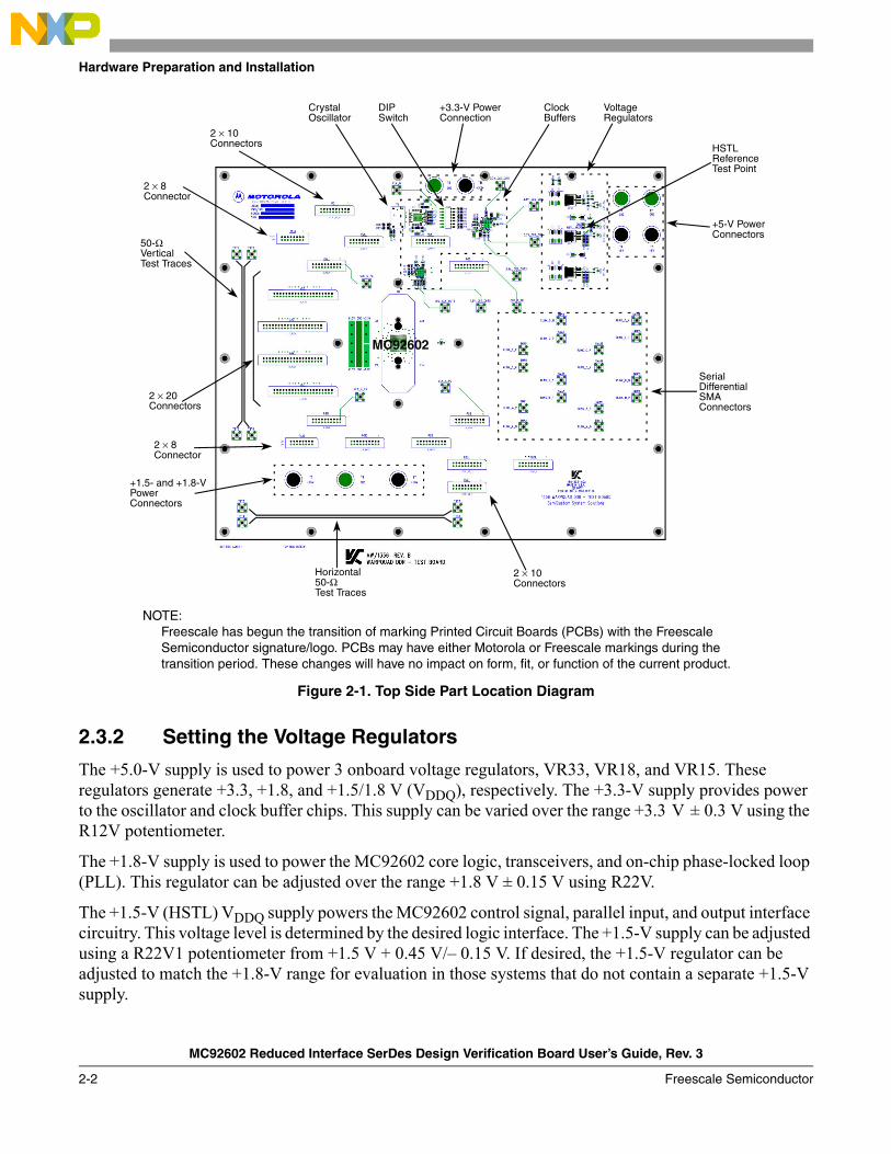
2.4 Reference Clock SourceThrough a combination of clock buffers, a reference clock is supplied to the MC92602 and several SMA output connectors. The input reference clock for the MC92602 can be supplied using either an onboard crystal oscillator, or by directly driving an external reference clock into the boards clock buffer circuit via SMA connector, CLK_IN. The clock circuitry for the MC92602DVB is shown in Figure 2-2.
Figure 2-2. MC92602DVB Clock Circuitry
Y2
Y1
EN
EN
ENCLK_0
REF_CLK_P
CLK
CLK
DIV 1/2
CSELDIV 1/2
DIV by 1
REF_CLK_N
1
7
SW1
U2
U3
MC100ES6222
MPC9456
250-MHzOscillator
+
+
CLK_1
CLK_IN
3.3V_CLK_OUT1
3.3V_CLK_OUT2
3.3V_CLK_OUT3
3.3V_CLK_OUT4
23456
1.5V_CLK_OUT5
1.5V_CLK_OUT6
DIV 1/2
U4 MC100ES8111
PECLto
HSTLBuffer

Hardware Preparation and Installation
MC92602 Reduced Interface SerDes Design Verification Board User’s Guide, Rev. 3
2-4 Freescale Semiconductor
2.4.1 Using the Onboard Oscillator
There are two available positions for using onboard oscillators. A standard 14-pin DIP socket is available on the board to allow the user to easily change frequencies by swapping in crystal oscillators with other values. The onboard oscillators must be two times (2×) the desired MVC92602 reference clock frequency. The default reference clock frequency oscillator supplied with the board is 250 MHz.
Crystal oscillators used with this board should have +3.3-V complementary PECL outputs capable of driving a line terminated with 50 Ω . Oscillators conforming to these specifications are also available in J-lead SMT packages and can be soldered onto the underside of the MC92602DVB at location Y2. This oscillator, Y2, can then be enabled by placing SW1 switch 1 in the off position. Both types of crystal oscillators are available from external vendors in a variety of frequencies. Once either type of oscillator is installed, SW1 switch 2 must be placed in the on position to select the onboard oscillator.
2.4.2 External Reference Clock Source
The input reference clock can also be supplied by using an external reference clock into the clock buffer circuit on the board via the CLK_IN SMA connector. To supply an external reference clock, switch number 2 on SW1 must be set to the off position. The user must then supply a 1.0-Vp-p input clock via the SMA connector. The CLK_IN input is AC coupled on the board and, therefore, does not require any DC biasing of the input signal. This external clock input is also terminated with a 50-Ω impedance.
2.4.3 Supplying a Clock to the MC92602
The input reference clock, from either the onboard oscillator or an external source, is applied to a MC100ES6222 clock buffer. This buffer has an input clock select multiplexer, and a programmable divide-by-one/divide-by-two function. The buffer also contains a master reset (Enable). It is recommended that this reset, found on SW1 switch 4, be activated, then deactivated after changing the divide-by-xx switch. This will ensure proper frequency generation.
Between the MC100ES6222 output and the MC92602 reference clock inputs, REF_CLK_P and REF_CLK_N, is an MC100ES8111 which performs a PECL to HSTL level shift. It also drives two SMA connectors, 1.5V_CLK_OUT5 and 1.5V_CLK_OUT6, with HSTL level clock signals.
NOTEThe outputs of the MCP100ES8111 expect to see a DC 50-Ω path to ground. Therefore, if a DC blocker is being used with the 1.5V_CLK_OUT5 or 1.5V_CLK_OUT6 outputs as a trigger or signal to an oscilloscope, a 50-Ω feed through termination must be placed in line before the DC blocker and before the attachment to the oscilloscope. A 3dB attenuator may be used in place of the 50-Ω feed through termination.

Hardware Preparation and Installation
MC92602 Reduced Interface SerDes Design Verification Board User’s Guide, Rev. 3
Freescale Semiconductor 2-5
2.4.4 3.3V_CLK_OUTn SMA Connectors
Four single-ended, 3.3-V level, clock signals are available on SMA connectors to drive other instruments. Between the MC100ES8111 output and the 4 SMAs, is an MPC9456 which performs a differential PECL to single-ended +3.3-V LVTTL/CMOS level shift. These CMOS outputs are series terminated on the board, then connect to the SMA connectors labeled 3.3V_CLK_OUT1, 3.3V_CLK_OUT2, 3.3V_CLK_OUT3, and 3.3V_CLK_OUT4. All of the outputs of the MPC9456 can be disabled by setting the DIP switch SW1, switch 7 to the off position.
2.4.5 Clock Frequency Selection
To accommodate the fact that the MC92602 can receive data on both edges of the reference clock (DDR), of which many pieces of test equipment are single-edge triggered (SDR), the MC92602DVB clock outputs can be programmed to be either the same as the supplied frequency or half the supplied frequency by setting SW1, switches 3, 5, and 6 to either on (divide-by-one) or to off (divide-by-2). This allows the interface between the board and the bench to be either single data rate (SDR) with a double speed clock, or double data rate (DDR) with a single speed clock.
The 1.5V_CLK_OUTn SMA outputs will always follow the clock supplied to the MC92602 and the frequency is programmed via SW1, switch 3. SMA outputs 3.3V_CLK_OUT1 and 3.3V_CLK_OUT2 can be programmed by setting SW1, switch 5 and 3.3V_CLK_OUT3 and 3.3V_CLK_OUT4 can be programmed by setting SW1, switch 6. Table 2-2 lists the switch positions and output frequencies. The input frequency, CLK_IN refers to either the onboard oscillator frequency or the externally applied clock source frequency.
NOTEOnly those frequencies listed in the MC92602 Quad 1.25 Gbaud Reduced Interface SerDes Reference Guide are considered valid. Freescale does not guarantee operation of the MC92602 at frequencies other than those listed in the reference Guide.
Table 2-2. SW1 Settings and Output Frequencies
SW1Switch
SwitchPosition
MC92602REF_CLK_P, REF_CLK_N,
and 1.5V_CLK_OUTn
3.3V_CLK_OUT1,3.3V_CLK_OUT2
3.3V_CLK_OUT,3.3V_CLK_OUT4
3 On CLK_IN N/A N/A
Off CLK_IN/2 N/A N/A
5 On N/A CLK_IN N/A
Off N/A CLK_IN/2 N/A
6 On N/A N/A CLK_IN
Off N/A N/A CLK_IN/2
Hardware Preparation and Installation
MC92602 Reduced Interface SerDes Design Verification Board User’s Guide, Rev. 3
2-6 Freescale Semiconductor
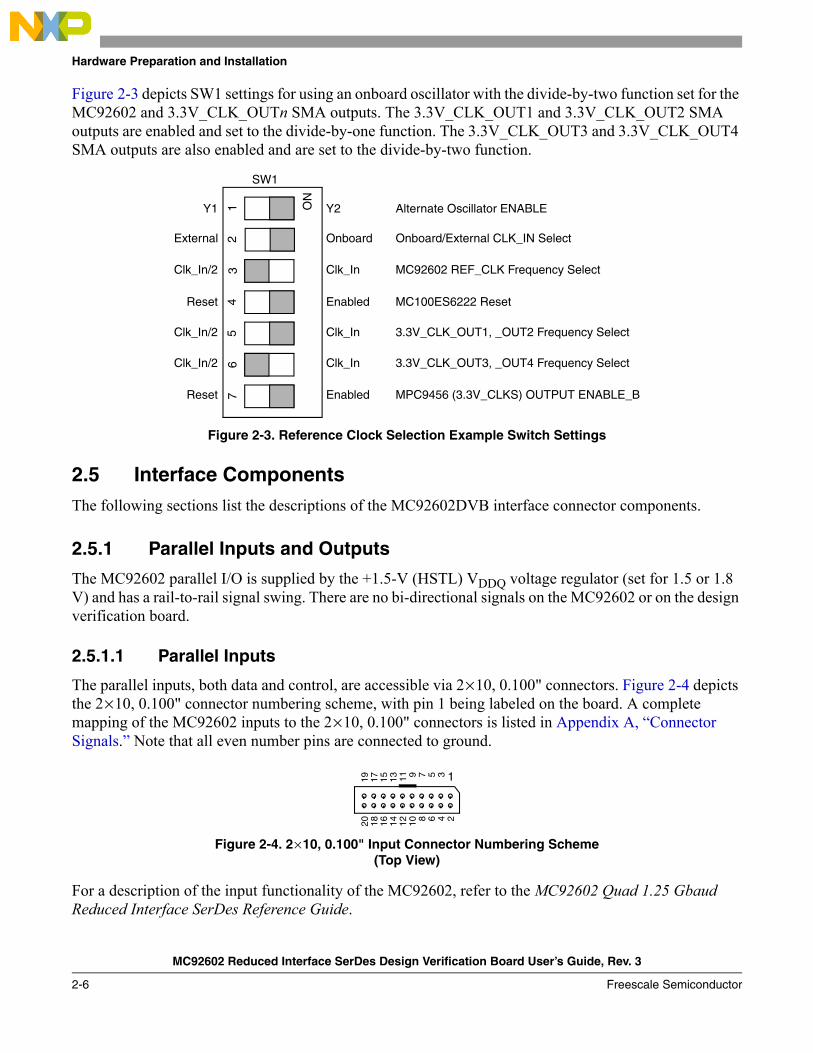
Figure 2-3 depicts SW1 settings for using an onboard oscillator with the divide-by-two function set for the MC92602 and 3.3V_CLK_OUTn SMA outputs. The 3.3V_CLK_OUT1 and 3.3V_CLK_OUT2 SMA outputs are enabled and set to the divide-by-one function. The 3.3V_CLK_OUT3 and 3.3V_CLK_OUT4 SMA outputs are also enabled and are set to the divide-by-two function.
Figure 2-3. Reference Clock Selection Example Switch Settings
2.5 Interface ComponentsThe following sections list the descriptions of the MC92602DVB interface connector components.
2.5.1 Parallel Inputs and Outputs
The MC92602 parallel I/O is supplied by the +1.5-V (HSTL) VDDQ voltage regulator (set for 1.5 or 1.8 V) and has a rail-to-rail signal swing. There are no bi-directional signals on the MC92602 or on the design verification board.
2.5.1.1 Parallel Inputs
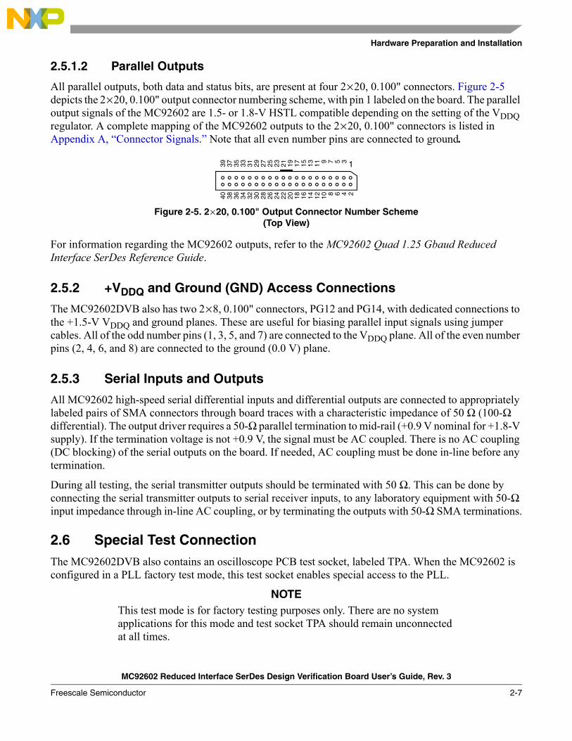
The parallel inputs, both data and control, are accessible via 2 × 10, 0.100" connectors. Figure 2-4 depicts the 2 × 10, 0.100" connector numbering scheme, with pin 1 being labeled on the board. A complete mapping of the MC92602 inputs to the 2 × 10, 0.100" connectors is listed in Appendix A, Connector Signals. Note that all even number pins are connected to ground.
Figure 2-4. 2 × 10, 0.100" Input Connector Numbering Scheme(Top View)
For a description of the input functionality of the MC92602, refer to the MC92602 Quad 1.25 Gbaud Reduced Interface SerDes Reference Guide.
12
34
56
ON
SW1
Onboard/External CLK_IN Select
MC92602 REF_CLK Frequency Select
MC100ES6222 Reset
3.3V_CLK_OUT1, _OUT2 Frequency Select
3.3V_CLK_OUT3, _OUT4 Frequency Select
MPC9456 (3.3V_CLKS) OUTPUT ENABLE_B7
Alternate Oscillator ENABLEY1
External
Clk_In/2
Reset
Clk_In/2
Clk_In/2
Reset
Y2
Onboard
Clk_In
Enabled
Clk_In
Clk_In
Enabled
1
23
45
67
89
1011
1213
1415
1617
1819
20
Hardware Preparation and Installation
MC92602 Reduced Interface SerDes Design Verification Board User’s Guide, Rev. 3
Freescale Semiconductor 2-7
2.5.1.2 Parallel Outputs
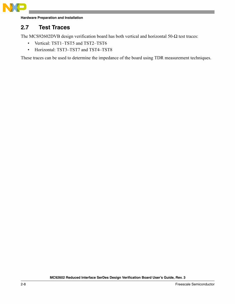
All parallel outputs, both data and status bits, are present at four 2 × 20, 0.100" connectors. Figure 2-5 depicts the 2 × 20, 0.100" output connector numbering scheme, with pin 1 labeled on the board. The parallel output signals of the MC92602 are 1.5- or 1.8-V HSTL compatible depending on the setting of the VDDQ regulator. A complete mapping of the MC92602 outputs to the 2 × 20, 0.100" connectors is listed in Appendix A, Connector Signals. Note that all even number pins are connected to ground.
Figure 2-5. 2 × 20, 0.100" Output Connector Number Scheme(Top View)
For information regarding the MC92602 outputs, refer to the MC92602 Quad 1.25 Gbaud Reduced Interface SerDes Reference Guide.
2.5.2 +VDDQ and Ground (GND) Access Connections
The MC92602DVB also has two 2 × 8, 0.100" connectors, PG12 and PG14, with dedicated connections to the +1.5-V VDDQ and ground planes. These are useful for biasing parallel input signals using jumper cables. All of the odd number pins (1, 3, 5, and 7) are connected to the VDDQ plane. All of the even number pins (2, 4, 6, and 8) are connected to the ground (0.0 V) plane.
2.5.3 Serial Inputs and Outputs
All MC92602 high-speed serial differential inputs and differential outputs are connected to appropriately labeled pairs of SMA connectors through board traces with a characteristic impedance of 50 Ω (100-Ω differential). The output driver requires a 50-Ω parallel termination to mid-rail (+0.9 V nominal for +1.8-V supply). If the termination voltage is not +0.9 V, the signal must be AC coupled. There is no AC coupling (DC blocking) of the serial outputs on the board. If needed, AC coupling must be done in-line before any termination.
During all testing, the serial transmitter outputs should be terminated with 50 Ω . This can be done by connecting the serial transmitter outputs to serial receiver inputs, to any laboratory equipment with 50-Ω input impedance through in-line AC coupling, or by terminating the outputs with 50-Ω SMA terminations.
2.6 Special Test ConnectionThe MC92602DVB also contains an oscilloscope PCB test socket, labeled TPA. When the MC92602 is configured in a PLL factory test mode, this test socket enables special access to the PLL.
NOTEThis test mode is for factory testing purposes only. There are no system applications for this mode and test socket TPA should remain unconnected at all times.
1
23
45
67
89
1011
1213
1415
1617
1819
2021
2223
2425
2627
2829
3031
3233
3435
3637
3839
40
Hardware Preparation and Installation
MC92602 Reduced Interface SerDes Design Verification Board User’s Guide, Rev. 3
2-8 Freescale Semiconductor
2.7 Test TracesThe MCS92602DVB design verification board has both vertical and horizontal 50-Ω test traces:
Vertical: TST1TST5 and TST2TST6 Horizontal: TST3TST7 and TST4TST8
These traces can be used to determine the impedance of the board using TDR measurement techniques.
MC92602 Reduced Interface SerDes Design Verification Board User’s Guide, Rev. 3
Freescale Semiconductor 3-1
Chapter 3 Laboratory Equipment and Quick Setup EvaluationThis chapter begins with a listing of the recommended test equipment needed to perform complete evaluations on the MC92602. Chapter 4, Test Setups, covers specific setup configurations for this equipment depending on the desired feature under test.
The quick setup evaluation procedures outlined below describe how the MC92602DVB can be used to evaluate the data eye diagram and a simple error rate test using the internal test features of the MC92602 with a minimal amount of test equipment. Only a power supply and sampling oscilloscope are required.
Details of testing in specific systems is left to the user. For more information regarding the MC92602 feature set, refer to the MC92602 Quad 1.25 Gbaud Reduced Interface SerDes Reference Guide.
3.1 Recommended Laboratory EquipmentEvaluation of the MC92602 feature set is possible using the MC92602DVB evaluation kit in conjunction with several pieces of test equipment. The quick setup evaluations and other tests listed in this guide utilize the basic set of test equipment listed in Table 3-1. Equivalent instrumentation may be substituted. Not all pieces of test equipment are necessary for all tests.
Table 3-1. Recommended Test Equipment
Quantity Equipment
1 MC92602DVB evaluation kit
1 Tektronix TDS 8000 digital sampling oscilloscope
1 Tektronix 80E04 TDR/sampling head (20 GHz)
3 Tektronix 80E03 sampling heads (20 GHz)
1 Hewlett-Packard HP16700 logic analysis system
5 Hewlett-Packard HP16522A pattern generators
2 Hewlett-Packard HP16557D logic analyzers
1 Hewlett Packard HP6624A system DC power supply
Laboratory Equipment and Quick Setup Evaluation
MC92602 Reduced Interface SerDes Design Verification Board User’s Guide, Rev. 3
3-2 Freescale Semiconductor
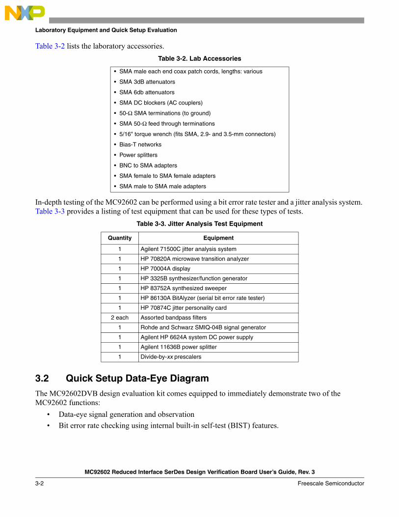
Table 3-2 lists the laboratory accessories.
In-depth testing of the MC92602 can be performed using a bit error rate tester and a jitter analysis system. Table 3-3 provides a listing of test equipment that can be used for these types of tests.
3.2 Quick Setup Data-Eye DiagramThe MC92602DVB design evaluation kit comes equipped to immediately demonstrate two of the MC92602 functions:
Data-eye signal generation and observation Bit error rate checking using internal built-in self-test (BIST) features.
Table 3-2. Lab Accessories
• SMA male each end coax patch cords, lengths: various
• SMA 3dB attenuators
• SMA 6db attenuators
• SMA DC blockers (AC couplers)
• 50-Ω SMA terminations (to ground)
• SMA 50-Ω feed through terminations
• 5/16" torque wrench (fits SMA, 2.9- and 3.5-mm connectors)
• Bias-T networks
• Power splitters
• BNC to SMA adapters
• SMA female to SMA female adapters
• SMA male to SMA male adapters
Table 3-3. Jitter Analysis Test Equipment
Quantity Equipment
1 Agilent 71500C jitter analysis system
1 HP 70820A microwave transition analyzer
1 HP 70004A display
1 HP 3325B synthesizer/function generator
1 HP 83752A synthesized sweeper
1 HP 86130A BitAlyzer (serial bit error rate tester)
1 HP 70874C jitter personality card
2 each Assorted bandpass filters
1 Rohde and Schwarz SMIQ-04B signal generator
1 Agilent HP 6624A system DC power supply
1 Agilent 11636B power splitter
1 Divide-by-xx prescalers
Laboratory Equipment and Quick Setup Evaluation
MC92602 Reduced Interface SerDes Design Verification Board User’s Guide, Rev. 3
Freescale Semiconductor 3-3
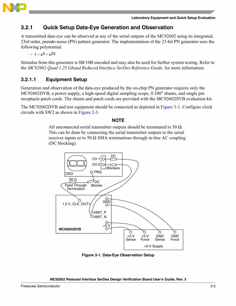
3.2.1 Quick Setup Data-Eye Generation and Observation
A transmitted data-eye can be observed at any of the serial outputs of the MC92602 using its integrated, 23rd order, pseudo-noise (PN) pattern generator. The implementation of the 23-bit PN generator uses the following polynomial.
Stimulus from this generator is 8B/10B encoded and may also be used for further system testing. Refer to the MC92602 Quad 1.25 Gbaud Reduced Interface SerDes Reference Guide, for more information.
3.2.1.1 Equipment Setup
Generation and observation of the data-eye produced by the on-chip PN generator requires only the MC92602DVB, a power supply, a high-speed digital sampling scope, 0.100" shunts, and single pin receptacle patch cords. The shunts and patch cords are provided with the MC92602DVB evaluation kit.
The MC92602DVB and test equipment should be connected as depicted in Figure 3-1. Configure clock circuits with SW2 as shown in Figure 2-3.
NOTEAll unconnected serial transmitter outputs should be terminated to 50 Ω . This can be done by connecting the serial transmitter outputs to the serial receiver inputs or to 50 Ω SMA terminations through in-line AC coupling (DC blocking).
Figure 3-1. Data-Eye Observation Setup
f 1 x5 x23+ +=
MC92602DVB
+5-V Supply
+5-V GND+5-V GND
+5 V
GND
XMIT_NXMIT_P
1.5 V_CLK_OUT1
CH 1
CH 2
TRIG
DCBlocker
DC
Blockers
DSO
Sense Force Sense Force
50 Ω
Feed ThroughTermination
Laboratory Equipment and Quick Setup Evaluation
MC92602 Reduced Interface SerDes Design Verification Board User’s Guide, Rev. 3
3-4 Freescale Semiconductor
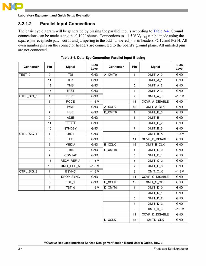
3.2.1.2 Parallel Input Connections
The basic eye diagram will be generated by biasing the parallel inputs according to Table 3-4. Ground connections can be made using the 0.100" shunts. Connections to +1.5 V VDDQ can be made using the square pin receptacle patch cords and jumpering to the odd numbered pins of headers PG12 and PG14. All even number pins on the connector headers are connected to the boards ground plane. All unlisted pins are not connected.
Table 3-4. Data-Eye Generation Parallel Input Biasing
Connector Pin SignalBiasLevel
Connector Pin SignalBiasLevel
TEST_0 9 TDI GND A_XMIT0 1 XMIT_A_0 GND
11 TCK GND 3 XMIT_A_1 GND
13 TMS GND 5 XMIT_A_2 GND
15 TRST GND 7 XMIT_A_3 GND
CTRL_SIG_0 1 REPE GND 9 XMIT_A_K +1.5 V
3 RCCE +1.5 V 11 XCVR_A_DISABLE GND
5 WSE GND A_XCLK 15 XMIT_A_CLK GND
7 HSE GND B_XMIT0 1 XMIT_B_0 GND
9 ADIE GND 3 XMIT_B_1 GND
11 RESET GND 5 XMIT_B_2 GND
15 STNDBY GND 7 XMIT_B_3 GND
CTRL_SIG_1 1 LBOE GND 9 XMIT_B_K +1.5 V
3 LBE GND 11 XCVR_B_DISABLE GND
5 MEDIA GND B_XCLK 15 XMIT_B_CLK GND
7 TBIE GND C_XMIT0 1 XMIT_C_0 GND
9 COMPAT GND 3 XMIT_C_1 GND
13 RECV_REF_A +1.5 V 5 XMIT_C_2 GND
15 XMIT_REF_A +1.5 V 7 XMIT_C_3 GND
CTRL_SIG_2 1 BSYNC +1.5 V 9 XMIT_C_K +1.5 V
3 DROP_SYNC GND 11 XCVR_C_DISABLE GND
5 TST_1 GND C_XCLK 15 XMIT_C_CLK GND
7 TST_0 +1.5 V D_XMIT0 1 XMIT_D_0 GND
3 XMIT_D_1 GND
5 XMIT_D_2 GND
7 XMIT_D_3 GND
9 XMIT_D_K +1.5 V
11 XCVR_D_DISABLE GND
D_XCLK 15 XMITD_CLK GND
Laboratory Equipment and Quick Setup Evaluation
MC92602 Reduced Interface SerDes Design Verification Board User’s Guide, Rev. 3
Freescale Semiconductor 3-5
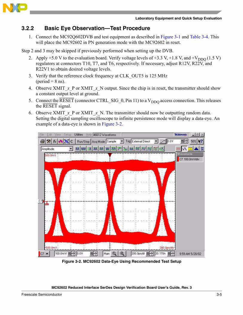
3.2.2 Basic Eye Observation—Test Procedure1. Connect the MC92Q602DVB and test equipment as described in Figure 3-1 and Table 3-4. This
will place the MC92602 in PN generation mode with the MC92602 in reset.
Step 2 and 3 may be skipped if previously performed when setting up the DVB.2. Apply +5.0 V to the evaluation board. Verify voltage levels of +3.3 V, +1.8 V, and +VDDQ (1.5 V)
regulators at connectors T10, T7, and T6, respectively. If necessary, adjust R12V, R22V, and R22V1 to obtain desired voltage levels.
3. Verify that the reference clock frequency at CLK_OUT5 is 125 MHz (period = 8 ns).
4. Observe XMIT_x_P or XMIT_x_N output. Since the chip is in reset, the transmitter should show a constant output level at ground.
5. Connect the RESET (connector CTRL_SIG_0, Pin 11) to a VDDQ access connection. This releases the RESET signal.
6. Observe XMIT_x_P or XMIT_x_N. The transmitter should now be outputting random data. Setting the digital sampling oscilloscope to infinite persistence mode will display a data-eye. An example of a data-eye is shown in Figure 3-2.
Figure 3-2. MC92602 Data-Eye Using Recommended Test Setup
Laboratory Equipment and Quick Setup Evaluation
MC92602 Reduced Interface SerDes Design Verification Board User’s Guide, Rev. 3
3-6 Freescale Semiconductor
3.2.3 Quick Setup Bit Error Rate Checking
In addition to having an integrated PN generator, the MC92602 also has a bit error rate checker (BERC). An integrated 23rd order signature analyzer, that is synchronized to the incoming PN stream is used to count code group mismatch errors relative to the internal PN reference pattern. The following test procedure will describe how to use this BIST feature. For more information concerning the MC92602 BIST, refer to the MC92602 Quad 1.25 Gbaud Reduced Interface SerDes Reference Guide.
3.2.3.1 Equipment Setup
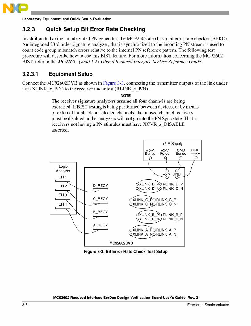
Connect the MC92602DVB as shown in Figure 3-3, connecting the transmitter outputs of the link under test (XLINK_x_P/N) to the receiver under test (RLINK_x_P/N).
NOTE
The receiver signature analyzers assume all four channels are being exercised. If BIST testing is being performed between devices, or by means of external loopback on selected channels, the unused channel receivers must be disabled or the analyzers will not go into the PN Sync state. That is, receivers not having a PN stimulus must have XCVR_x_DISABLE asserted.
Figure 3-3. Bit Error Rate Check Test Setup
XLINK_A_NXLINK_A_P
MC92602DVB
+5-V Supply
+5-V GND+5-V GND
+5 V GND
RLINK_D_NRLINK_D_P
XLINK_D_NXLINK_D_PD_RECV
C_RECV
B_RECV
A_RECV
CH 1
CH 2
CH 3
CH 4
Sense Force Sense Force
LogicAnalyzer
RLINK_C_NRLINK_C_P
XLINK_C_NXLINK_C_P
RLINK_B_NRLINK_B_P
XLINK_B_NXLINK_B_P
RLINK_A_NRLINK_A_P
Laboratory Equipment and Quick Setup Evaluation
MC92602 Reduced Interface SerDes Design Verification Board User’s Guide, Rev. 3
Freescale Semiconductor 3-7
3.2.3.2 Parallel I/O Connections
The bias connections for the parallel inputs to perform the quick setup BERC test are the same as those for the quick setup eye-diagram and shown in Table 3-4.
The parallel outputs are connected to a data analysis system. The data analyzer may be used to observe the start up sequence and the status and errors detected by the internal data analyzers.
3.2.3.3 Quick Setup BERC Test Procedure
1. Connect the MC92602DVB and test equipment as described in Section 3.2.3.1, Equipment Setup. This will place the MC92602 in PN generation mode with the MC92602 held in reset and set the receivers to BERC mode using the recovered clock.
Steps 2 and 3 may be skipped if previously performed when setting up the DVB.2. Apply +5.0 V to the evaluation board. Verify voltage levels of +3.3 V, +1.8 V, and +VDDQ (1.5 V)
regulators at connectors T10, T7, and T6, respectively. If necessary, adjust R12V, R22V, and R22V1 to obtain desired voltage levels.
3. Verify that the reference clock frequency at CLK_OUT1 is 156.25 MHz (period = 6.4 ns).
4. Connect the RESET (connector CTRL_SIG_0, pin 11) to a +1.5 V VDDQ access connection. This releases the RESET signal.
5. Observe the parallel outputs on the data analyzer. As described in the MC92602 Quad 1.25 Gbaud Reduced Interface SerDes Reference Guide, the MC92602 will start and lock the PLL, initialize the receivers, perform byte alignment, and reset the bit error counter.
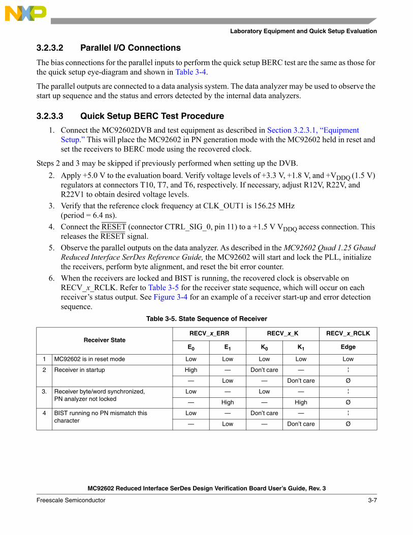
6. When the receivers are locked and BIST is running, the recovered clock is observable on RECV_x_RCLK. Refer to Table 3-5 for the receiver state sequence, which will occur on each receivers status output. See Figure 3-4 for an example of a receiver start-up and error detection sequence.
Table 3-5. State Sequence of Receiver
Receiver StateRECV_x_ERR RECV_x_K RECV_x_RCLK
E0 E1 K0 K1 Edge
1 MC92602 is in reset mode Low Low Low Low Low
2 Receiver in startup High — Don’t care — ¦
— Low — Don’t care Ø
3. Receiver byte/word synchronized, PN analyzer not locked
Low — Low — ¦
— High — High Ø
4 BIST running no PN mismatch this character
Low — Don’t care — ¦
— Low — Don’t care Ø
Laboratory Equipment and Quick Setup Evaluation
MC92602 Reduced Interface SerDes Design Verification Board User’s Guide, Rev. 3
3-8 Freescale Semiconductor
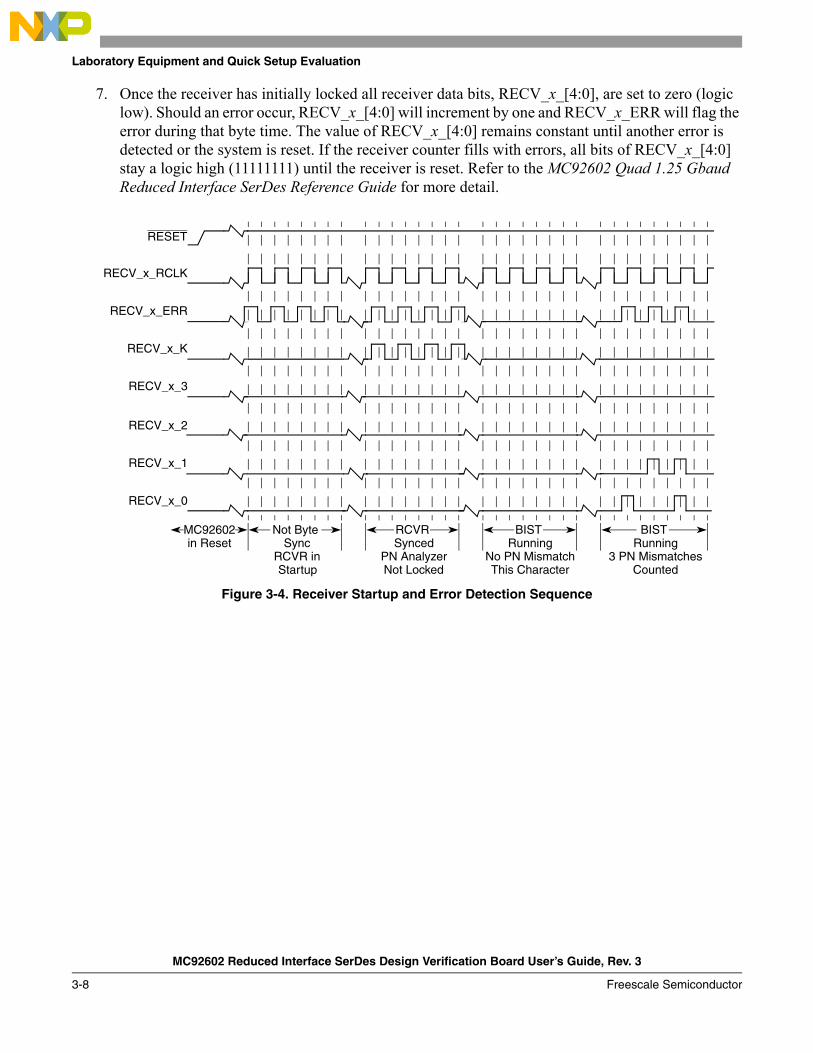
7. Once the receiver has initially locked all receiver data bits, RECV_x_[4:0], are set to zero (logic low). Should an error occur, RECV_x_[4:0] will increment by one and RECV_x_ERR will flag the error during that byte time. The value of RECV_x_[4:0] remains constant until another error is detected or the system is reset. If the receiver counter fills with errors, all bits of RECV_x_[4:0] stay a logic high (11111111) until the receiver is reset. Refer to the MC92602 Quad 1.25 Gbaud Reduced Interface SerDes Reference Guide for more detail.
Figure 3-4. Receiver Startup and Error Detection Sequence
BIST
Counted3 PN Mismatches
Running
RECV_x_RCLK
RECV_x_ERR
RECV_x_K
RECV_x_3
RESET
RECV_x_1
RECV_x_0
RECV_x_2
MC92602in Reset
RCVR BIST Not Byte
Not LockedPN Analyzer
Synced
This CharacterNo PN Mismatch
Running
StartupRCVR in
Sync
MC92602 Reduced Interface SerDes Design Verification Board User’s Guide, Rev. 3
Freescale Semiconductor 4-1
Chapter 4 Test SetupsThis chapter outlines the laboratory test equipment setup and procedure to evaluate the features of the MC92602 in more depth than those outlined in the previous chapter. These setups are meant to be guidelines only and are not implied to be complete. Details of testing in specific system applications are left to the user.
4.1 Serial Link Verification Using a Serial Bit Error Rate Tester (BERT)
This test setup is used to observe the rate at which the MC92602 produces errors given either pseudo-random (PRBS) patterns or user-defined pattern sets generated by the serial bit error rate tester (BERT). The MC92602 is placed in repeater mode, REPE = high, thereby disabling the parallel receiver and transmitter buses. Testing performed using the ten-bit interface mode does not require the insertion of idle characters for word recognition or byte alignment. If verification using the 8B/10B encoder or other MC92602 features is required, then appropriate idle insertion and timing requirements as outlined in the MC92602 Quad 1.25 Gbaud Reduced Interface SerDes Reference Guide, must be followed.
Test Setups
MC92602 Reduced Interface SerDes Design Verification Board User’s Guide, Rev. 3
4-2 Freescale Semiconductor
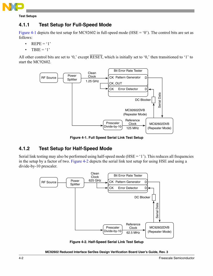
4.1.1 Test Setup for Full-Speed Mode
Figure 4-1 depicts the test setup for MC92602 in full-speed mode (HSE = 0). The control bits are set as follows:
REPE = 1 TBIE = 1
All other control bits are set to 0, except RESET, which is initially set to 0, then transitioned to 1 to start the MC92602.
Figure 4-1. Full Speed Serial Link Test Setup
4.1.2 Test Setup for Half-Speed Mode
Serial link testing may also be performed using half-speed mode (HSE = 1). This reduces all frequencies in the setup by a factor of two. Figure 4-2 depicts the serial link test setup for using HSE and using a divide-by-10 prescaler.
Figure 4-2. Half-Speed Serial Link Test Setup
CK Error Detector D
CK Pattern Generator D
Bit Error Rate TesterCleanClock
1.25 GHz
PowerSplitter
PrescalerDivide-by-10
Ser
ial D
ata
ReferenceClock
125 MHz
DC Blocker
CK_OUT
RF Source
MC92602DVB(Repeater Mode)
MC92602DVB(Repeater Mode)
RF Source
CK Error Detector D
CK Pattern Generator D
Bit Error Rate TesterCleanClock
625 GHzPowerSplitter
PrescalerDivide-by-10
MC92602DVB
Ser
ial D
ata
ReferenceClock
62.5 MHz (Repeater Mode)
DC Blocker
Test Setups
MC92602 Reduced Interface SerDes Design Verification Board User’s Guide, Rev. 3
Freescale Semiconductor 4-3
4.2 Jitter TestingThe following tests are guidelines for verifying the performance of the MC92602 in noisy conditions. Results will vary depending on input reference frequencies, MC92602 mode of operation, test setup and equipment, and test environment.
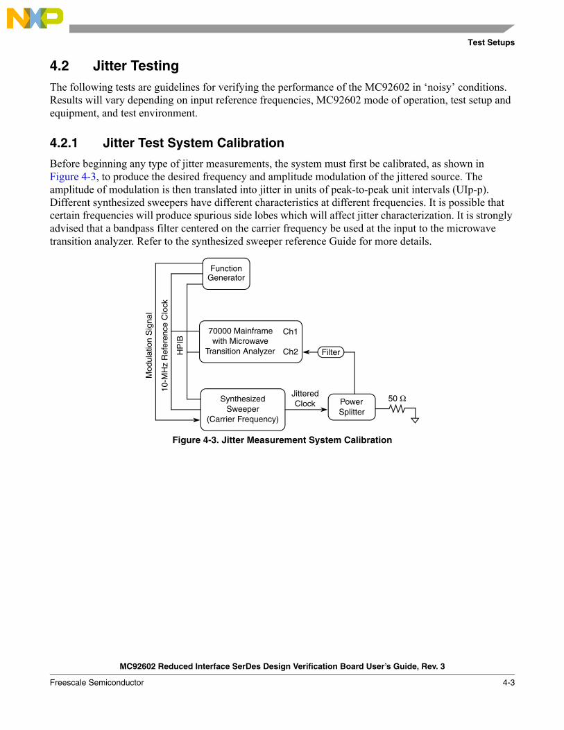
4.2.1 Jitter Test System Calibration
Before beginning any type of jitter measurements, the system must first be calibrated, as shown in Figure 4-3, to produce the desired frequency and amplitude modulation of the jittered source. The amplitude of modulation is then translated into jitter in units of peak-to-peak unit intervals (UIp-p). Different synthesized sweepers have different characteristics at different frequencies. It is possible that certain frequencies will produce spurious side lobes which will affect jitter characterization. It is strongly advised that a bandpass filter centered on the carrier frequency be used at the input to the microwave transition analyzer. Refer to the synthesized sweeper reference Guide for more details.
Figure 4-3. Jitter Measurement System Calibration
FunctionGenerator
Mod
ulat
ion
Sig
nal
10-M
Hz
Ref
eren
ce C
lock
HP
IB
PowerSplitter
JitteredClock
Filter
SynthesizedSweeper
(Carrier Frequency)
70000 Mainframewith Microwave
Transition Analyzer
Ch1
Ch2
50 Ω
Test Setups
MC92602 Reduced Interface SerDes Design Verification Board User’s Guide, Rev. 3
4-4 Freescale Semiconductor
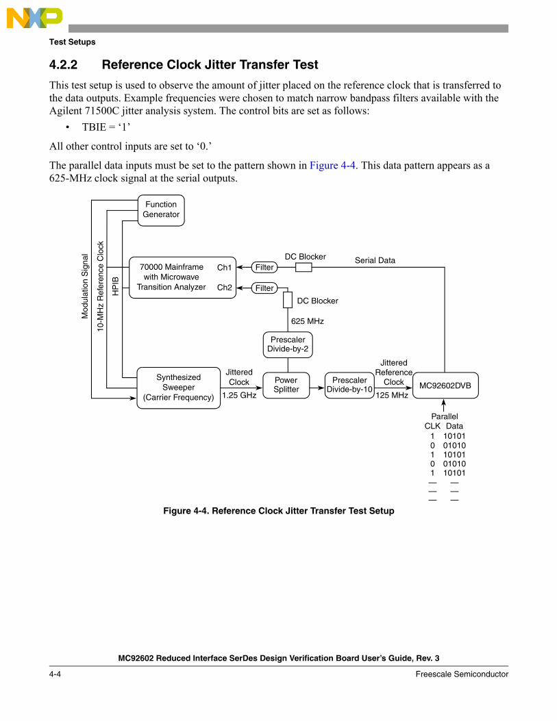
4.2.2 Reference Clock Jitter Transfer Test
This test setup is used to observe the amount of jitter placed on the reference clock that is transferred to the data outputs. Example frequencies were chosen to match narrow bandpass filters available with the Agilent 71500C jitter analysis system. The control bits are set as follows:
TBIE = 1
All other control inputs are set to 0.
The parallel data inputs must be set to the pattern shown in Figure 4-4. This data pattern appears as a 625-MHz clock signal at the serial outputs.
Figure 4-4. Reference Clock Jitter Transfer Test Setup
70000 Mainframewith Microwave
Transition Analyzer
Ch1
Ch2
FunctionGenerator
Mod
ulat
ion
Sig
nal
10-M
Hz
Ref
eren
ce C
lock
HP
IB
PowerSplitter
JitteredClock
1.25 GHz
PrescalerDivide-by-10 MC92602DVB
Serial Data
JitteredReference
Clock
125 MHz
Filter
Filter
Data
SynthesizedSweeper
(Carrier Frequency)
DC Blocker
10101
PrescalerDivide-by-2
DC Blocker
625 MHz
01010101010101010101
———
ParallelCLK
10101———

Test Setups
MC92602 Reduced Interface SerDes Design Verification Board User’s Guide, Rev. 3
Freescale Semiconductor 4-5
4.2.3 Reference Clock Jitter Tolerance Test
The test setup, as shown in Figure 4-5, is used to observe the amount of jitter placed on the reference clock that does not produce errors on the serial data outputs as compared to the input serial data stream. The MC92602 is placed in ten-bit interface mode (TBIE) and repeater mode (REPE). The serial data stream can be set to either PRBS or user-defined data. The control bits are set as follows:
REPE = 1 TBIE = 1
All other control inputs are set to 0.
Figure 4-5. Reference Clock Jitter Tolerance Test Setup
RF Source
70000 Mainframewith Microwave
Transition Analyzer
Ch1
Ch2
FunctionGenerator
Mod
ulat
ion
Sig
nal
10-M
Hz
Ref
eren
ce C
lock
HP
IB
CK Error Detector D
CK Pattern Generator D
Bit Error Rate TesterCleanClock
1.25 GHz
Bit Error Rate Data over the HPIB
PowerSplitter
JitteredClock
1.25 GHz
PrescalerDivide-by-10 MC92602DVB
Ser
ial D
ata
JitteredReference
Clock
125 MHz
SynthesizedSweeper
(Carrier Frequency)
DC Blocker

Test Setups
MC92602 Reduced Interface SerDes Design Verification Board User’s Guide, Rev. 3
4-6 Freescale Semiconductor
4.2.4 Data Jitter Tolerance Test
The test setup, as shown in Figure 4-6, is used to observe the amount of jitter placed on the serial data inputs that does not produce errors on the serial data outputs. The MC92602 is placed in ten-bit interface mode (TBIE) and repeater mode (REPE). The serial data stream can be set to either PRBS or user-defined data. The control bits are set as follows:
REPE = 1 TBIE = 1
All other control inputs are set to 0.
Figure 4-6. Data Jitter Tolerance Test Setup
RF Source
70000 Mainframewith Microwave
Transition Analyzer
Ch1
Ch2
FunctionGenerator
Mod
ulat
ion
Sig
nal
10-M
Hz
Ref
eren
ce C
lock
HP
IB
CK Error Detector D
CK Pattern Generator D
Bit Error Rate TesterCleanClock
1.25 GHz
Bit Error Rate Data Over the HPIB
PowerSplitter
Jittered Clock
1.25 GHz
PrescalerDivide-by-10
MC92602DVB
Ser
ial D
ata
ReferenceClock
125 MHz (Repeater Mode)
SynthesizedSweeper
(Carrier Frequency)
DC Blocker
MC92602 Reduced Interface SerDes Design Verification Board User’s Guide, Rev. 3
Freescale Semiconductor A-1
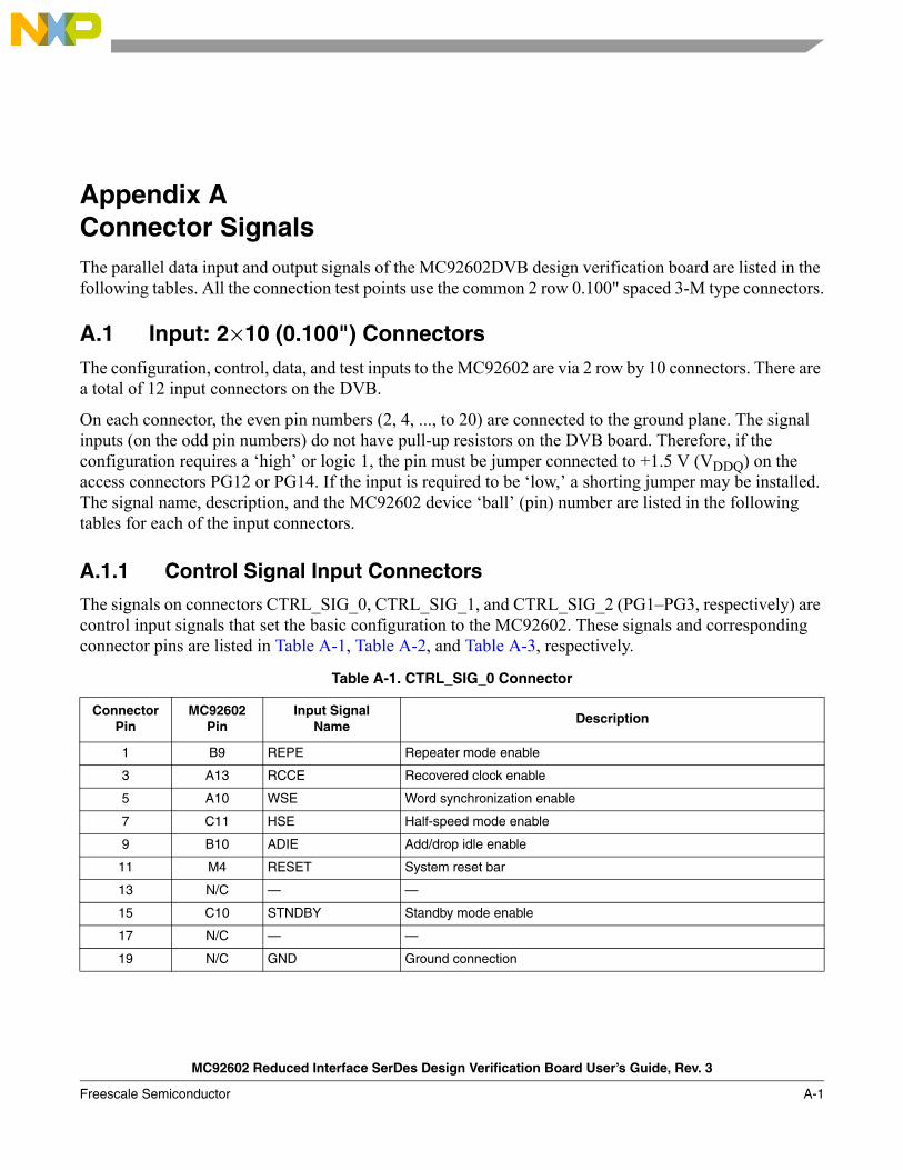
Appendix A Connector SignalsThe parallel data input and output signals of the MC92602DVB design verification board are listed in the following tables. All the connection test points use the common 2 row 0.100" spaced 3-M type connectors.
A.1 Input: 2 × 10 (0.100") ConnectorsThe configuration, control, data, and test inputs to the MC92602 are via 2 row by 10 connectors. There are a total of 12 input connectors on the DVB.
On each connector, the even pin numbers (2, 4, ..., to 20) are connected to the ground plane. The signal inputs (on the odd pin numbers) do not have pull-up resistors on the DVB board. Therefore, if the configuration requires a high or logic 1, the pin must be jumper connected to +1.5 V (VDDQ) on the access connectors PG12 or PG14. If the input is required to be low, a shorting jumper may be installed. The signal name, description, and the MC92602 device ball (pin) number are listed in the following tables for each of the input connectors.
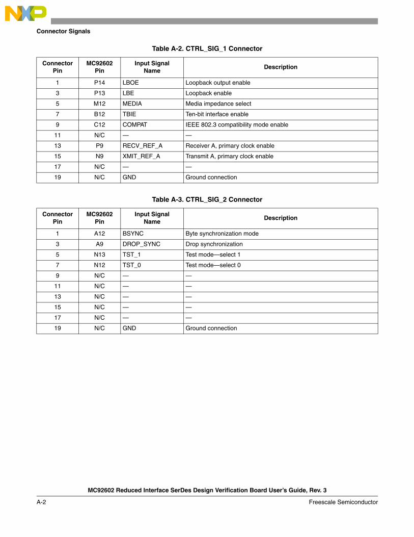
A.1.1 Control Signal Input Connectors
The signals on connectors CTRL_SIG_0, CTRL_SIG_1, and CTRL_SIG_2 (PG1PG3, respectively) are control input signals that set the basic configuration to the MC92602. These signals and corresponding connector pins are listed in Table A-1, Table A-2, and Table A-3, respectively.
Table A-1. CTRL_SIG_0 Connector
ConnectorPin
MC92602Pin
Input SignalName
Description
1 B9 REPE Repeater mode enable
3 A13 RCCE Recovered clock enable
5 A10 WSE Word synchronization enable
7 C11 HSE Half-speed mode enable
9 B10 ADIE Add/drop idle enable
11 M4 RESET System reset bar
13 N/C — —
15 C10 STNDBY Standby mode enable
17 N/C — —
19 N/C GND Ground connection
Connector Signals
MC92602 Reduced Interface SerDes Design Verification Board User’s Guide, Rev. 3
A-2 Freescale Semiconductor
Table A-2. CTRL_SIG_1 Connector
ConnectorPin
MC92602Pin
Input SignalName
Description
1 P14 LBOE Loopback output enable
3 P13 LBE Loopback enable
5 M12 MEDIA Media impedance select
7 B12 TBIE Ten-bit interface enable
9 C12 COMPAT IEEE 802.3 compatibility mode enable
11 N/C — —
13 P9 RECV_REF_A Receiver A, primary clock enable
15 N9 XMIT_REF_A Transmit A, primary clock enable
17 N/C — —
19 N/C GND Ground connection
Table A-3. CTRL_SIG_2 Connector
ConnectorPin
MC92602Pin
Input SignalName
Description
1 A12 BSYNC Byte synchronization mode
3 A9 DROP_SYNC Drop synchronization
5 N13 TST_1 Test mode—select 1
7 N12 TST_0 Test mode—select 0
9 N/C — —
11 N/C — —
13 N/C — —
15 N/C — —
17 N/C — —
19 N/C GND Ground connection
Connector Signals
MC92602 Reduced Interface SerDes Design Verification Board User’s Guide, Rev. 3
Freescale Semiconductor A-3
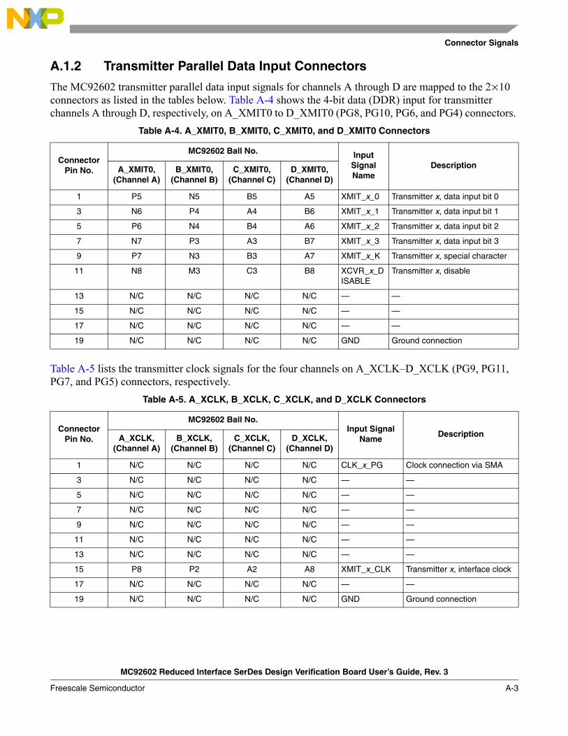
A.1.2 Transmitter Parallel Data Input Connectors
The MC92602 transmitter parallel data input signals for channels A through D are mapped to the 2 × 10 connectors as listed in the tables below. Table A-4 shows the 4-bit data (DDR) input for transmitter channels A through D, respectively, on A_XMIT0 to D_XMIT0 (PG8, PG10, PG6, and PG4) connectors.
Table A-5 lists the transmitter clock signals for the four channels on A_XCLKD_XCLK (PG9, PG11, PG7, and PG5) connectors, respectively.
Table A-4. A_XMIT0, B_XMIT0, C_XMIT0, and D_XMIT0 Connectors
Connector Pin No.
MC92602 Ball No. Input Signal Name
DescriptionA_XMIT0,(Channel A)
B_XMIT0,(Channel B)
C_XMIT0,(Channel C)
D_XMIT0,(Channel D)
1 P5 N5 B5 A5 XMIT_x_0 Transmitter x, data input bit 0
3 N6 P4 A4 B6 XMIT_x_1 Transmitter x, data input bit 1
5 P6 N4 B4 A6 XMIT_x_2 Transmitter x, data input bit 2
7 N7 P3 A3 B7 XMIT_x_3 Transmitter x, data input bit 3
9 P7 N3 B3 A7 XMIT_x_K Transmitter x, special character
11 N8 M3 C3 B8 XCVR_x_DISABLE
Transmitter x, disable
13 N/C N/C N/C N/C — —
15 N/C N/C N/C N/C — —
17 N/C N/C N/C N/C — —
19 N/C N/C N/C N/C GND Ground connection
Table A-5. A_XCLK, B_XCLK, C_XCLK, and D_XCLK Connectors
ConnectorPin No.
MC92602 Ball No.Input Signal
NameDescriptionA_XCLK,
(Channel A)B_XCLK,
(Channel B)C_XCLK,
(Channel C)D_XCLK,
(Channel D)
1 N/C N/C N/C N/C CLK_x_PG Clock connection via SMA
3 N/C N/C N/C N/C — —
5 N/C N/C N/C N/C — —
7 N/C N/C N/C N/C — —
9 N/C N/C N/C N/C — —
11 N/C N/C N/C N/C — —
13 N/C N/C N/C N/C — —
15 P8 P2 A2 A8 XMIT_x_CLK Transmitter x, interface clock
17 N/C N/C N/C N/C — —
19 N/C N/C N/C N/C GND Ground connection
Connector Signals
MC92602 Reduced Interface SerDes Design Verification Board User’s Guide, Rev. 3
A-4 Freescale Semiconductor
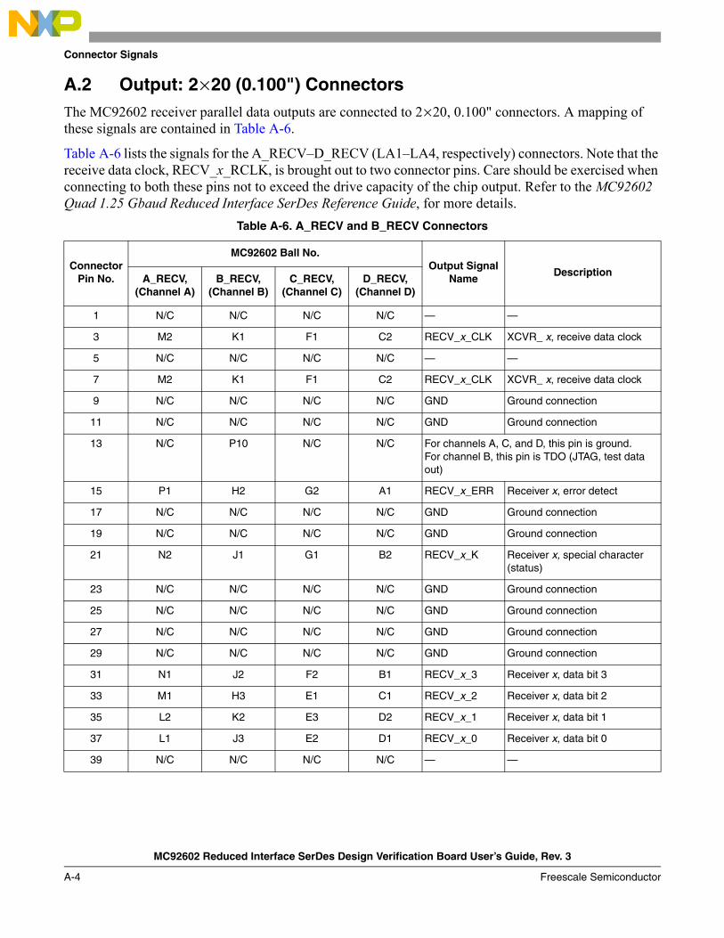
A.2 Output: 2 × 20 (0.100") ConnectorsThe MC92602 receiver parallel data outputs are connected to 2 × 20, 0.100" connectors. A mapping of these signals are contained in Table A-6.
Table A-6 lists the signals for the A_RECVD_RECV (LA1LA4, respectively) connectors. Note that the receive data clock, RECV_x_RCLK, is brought out to two connector pins. Care should be exercised when connecting to both these pins not to exceed the drive capacity of the chip output. Refer to the MC92602 Quad 1.25 Gbaud Reduced Interface SerDes Reference Guide, for more details.
Table A-6. A_RECV and B_RECV Connectors
ConnectorPin No.
MC92602 Ball No.Output Signal
NameDescription
A_RECV,(Channel A)
B_RECV,(Channel B)
C_RECV,(Channel C)
D_RECV,(Channel D)
1 N/C N/C N/C N/C — —
3 M2 K1 F1 C2 RECV_x_CLK XCVR_ x, receive data clock
5 N/C N/C N/C N/C — —
7 M2 K1 F1 C2 RECV_x_CLK XCVR_ x, receive data clock
9 N/C N/C N/C N/C GND Ground connection
11 N/C N/C N/C N/C GND Ground connection
13 N/C P10 N/C N/C For channels A, C, and D, this pin is ground.For channel B, this pin is TDO (JTAG, test data out)
15 P1 H2 G2 A1 RECV_x_ERR Receiver x, error detect
17 N/C N/C N/C N/C GND Ground connection
19 N/C N/C N/C N/C GND Ground connection
21 N2 J1 G1 B2 RECV_x_K Receiver x, special character (status)
23 N/C N/C N/C N/C GND Ground connection
25 N/C N/C N/C N/C GND Ground connection
27 N/C N/C N/C N/C GND Ground connection
29 N/C N/C N/C N/C GND Ground connection
31 N1 J2 F2 B1 RECV_x_3 Receiver x, data bit 3
33 M1 H3 E1 C1 RECV_x_2 Receiver x, data bit 2
35 L2 K2 E3 D2 RECV_x_1 Receiver x, data bit 1
37 L1 J3 E2 D1 RECV_x_0 Receiver x, data bit 0
39 N/C N/C N/C N/C — —
Connector Signals
MC92602 Reduced Interface SerDes Design Verification Board User’s Guide, Rev. 3
Freescale Semiconductor A-5
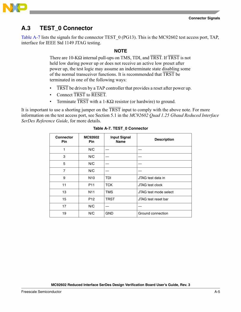
A.3 TEST_0 ConnectorTable A-7 lists the signals for the connector TEST_0 (PG13). This is the MC92602 test access port, TAP, interface for IEEE Std 1149 JTAG testing.
NOTEThere are 10-KΩ internal pull-ups on TMS, TDI, and TRST. If TRST is not held low during power up or does not receive an active low preset after power up, the test logic may assume an indeterminate state disabling some of the normal transceiver functions. It is recommended that TRST be terminated in one of the following ways:
TRST be driven by a TAP controller that provides a reset after power up. Connect TRST to RESET. Terminate TRST with a 1-KΩ resistor (or hardwire) to ground.
It is important to use a shorting jumper on the TRST input to comply with the above note. For more information on the test access port, see Section 5.1 in the MC92602 Quad 1.25 Gbaud Reduced Interface SerDes Reference Guide, for more details.
Table A-7. TEST_0 Connector
ConnectorPin
MC92602Pin
Input SignalName
Description
1 N/C — —
3 N/C — —
5 N/C — —
7 N/C — —
9 N10 TDI JTAG test data in
11 P11 TCK JTAG test clock
13 N11 TMS JTAG test mode select
15 P12 TRST JTAG test reset bar
17 N/C — —
19 N/C GND Ground connection

Connector Signals
MC92602 Reduced Interface SerDes Design Verification Board User’s Guide, Rev. 3
A-6 Freescale Semiconductor

MC92602 Reduced Interface SerDes Design Verification Board User’s Guide, Rev. 3
Freescale Semiconductor B-1
Appendix B Parts List
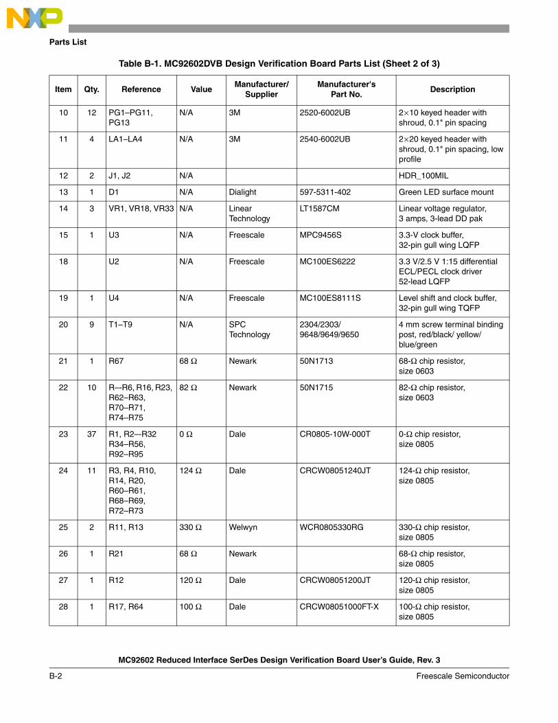
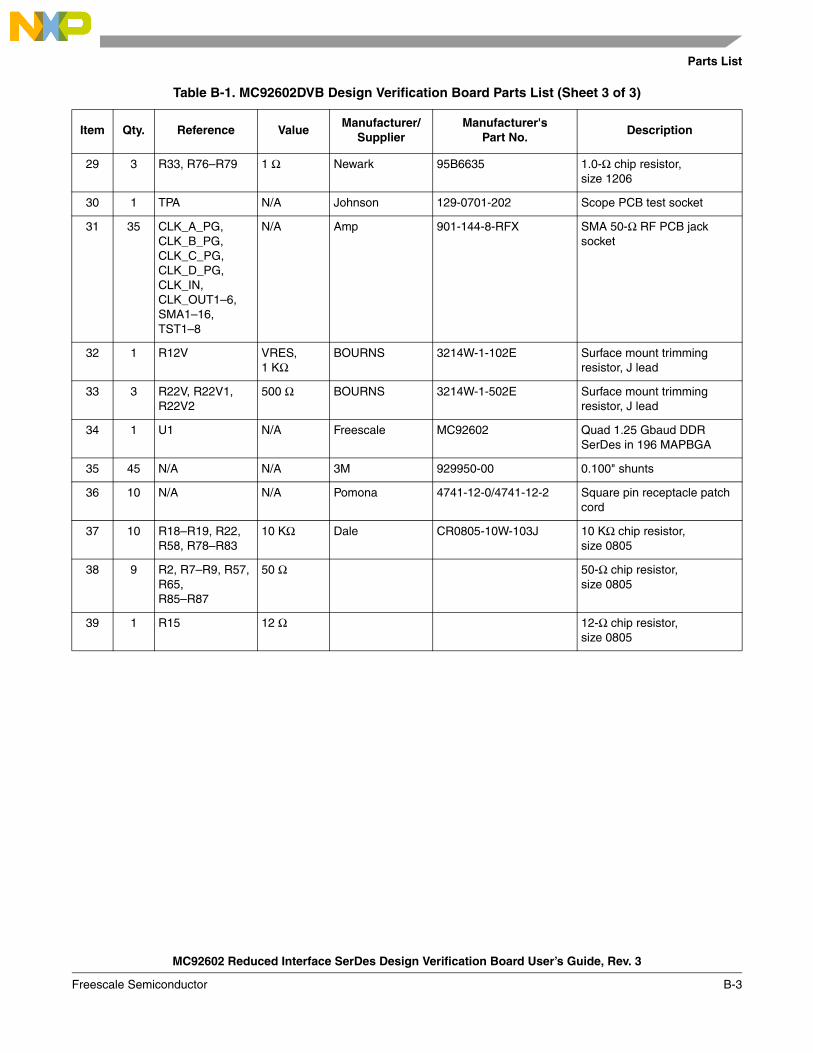
B.1 Design Verification Board Parts ListTable B-1 shows the parts used in constructing the MC92602DVB design verification board.
Table B-1. MC92602DVB Design Verification Board Parts List (Sheet 1 of 3)
Item Qty. Reference ValueManufacturer/
SupplierManufacturer's
Part No.Description
1 19 C1, C4, C18–C19, C24, C27, C30–C33, C54–C57, C208–C210, C303–C304
1 µF Newark 99F3410 Ceramic chip capacitor, 1 µF, size 1812
2 3 C7, C11, C21 100 µF Kemet T495X107K010AS 100 µF solid tantalum chip capacitor, low ESR, 10 V, size 7343H
3 5 C5, C12–C13, C22–C23
10 µF Kemet T495X106K035AS 10 µF solid tantalum chip capacitor, low ESR, 35 V, size 7343H
4 5 C3, C9, C10, C14, C20
0.1 µF Newark 93F8740 Ceramic chip capacitor, 0.1 µF, size 0805
5 45 C2, C5–C6, C15–C17, C25–C26, C28–C29, C34–C53, C58–C63, C201–C207, C301–302
0.01 µF Newark 93F2330 Ceramic chip capacitor, 0.01 µF, size 0805
6 1 Y1 250 MHz MF Electronics M2988-250M 250 MHz + 3.3 V PECL crystal oscillator—14-pin DIP
7 1 Y1 Socket N/A TTI 504-AG11D Socket, 14-pin DIP
8 1 SW1 N/A Newark 08C7815 7 pole DIP slide switches, 2 position (open or closed), surface mount
9 2 PG12, PG14 N/A 3M 2516-6002UB 2 × 8 keyed header with shroud, 0.1" pin spacing, low profile
Parts List
MC92602 Reduced Interface SerDes Design Verification Board User’s Guide, Rev. 3
B-2 Freescale Semiconductor
10 12 PG1–PG11, PG13
N/A 3M 2520-6002UB 2 × 10 keyed header with shroud, 0.1" pin spacing
11 4 LA1–LA4 N/A 3M 2540-6002UB 2 × 20 keyed header with shroud, 0.1" pin spacing, low profile
12 2 J1, J2 N/A HDR_100MIL
13 1 D1 N/A Dialight 597-5311-402 Green LED surface mount
14 3 VR1, VR18, VR33 N/A Linear Technology
LT1587CM Linear voltage regulator, 3 amps, 3-lead DD pak
15 1 U3 N/A Freescale MPC9456S 3.3-V clock buffer, 32-pin gull wing LQFP
18 U2 N/A Freescale MC100ES6222 3.3 V/2.5 V 1:15 differential ECL/PECL clock driver 52-lead LQFP
19 1 U4 N/A Freescale MC100ES8111S Level shift and clock buffer, 32-pin gull wing TQFP
20 9 T1–T9 N/A SPC Technology
2304/2303/ 9648/9649/9650
4 mm screw terminal binding post, red/black/ yellow/ blue/green
21 1 R67 68 Ω Newark 50N1713 68-Ω chip resistor, size 0603
22 10 R–-R6, R16, R23, R62–R63, R70–R71, R74–R75
82 Ω Newark 50N1715 82-Ω chip resistor, size 0603
23 37 R1, R2–-R32 R34–R56, R92–R95
0 Ω Dale CR0805-10W-000T 0-Ω chip resistor, size 0805
24 11 R3, R4, R10, R14, R20, R60–R61, R68–R69, R72–R73
124 Ω Dale CRCW08051240JT 124-Ω chip resistor, size 0805
25 2 R11, R13 330 Ω Welwyn WCR0805330RG 330-Ω chip resistor, size 0805
26 1 R21 68 Ω Newark 68-Ω chip resistor, size 0805
27 1 R12 120 Ω Dale CRCW08051200JT 120-Ω chip resistor, size 0805
28 1 R17, R64 100 Ω Dale CRCW08051000FT-X 100-Ω chip resistor, size 0805
Table B-1. MC92602DVB Design Verification Board Parts List (Sheet 2 of 3)
Item Qty. Reference ValueManufacturer/
SupplierManufacturer's
Part No.Description
Parts List
MC92602 Reduced Interface SerDes Design Verification Board User’s Guide, Rev. 3
Freescale Semiconductor B-3
29 3 R33, R76–R79 1 Ω Newark 95B6635 1.0-Ω chip resistor, size 1206
30 1 TPA N/A Johnson 129-0701-202 Scope PCB test socket
31 35 CLK_A_PG, CLK_B_PG, CLK_C_PG, CLK_D_PG, CLK_IN, CLK_OUT1–6, SMA1–16, TST1–8
N/A Amp 901-144-8-RFX SMA 50-Ω RF PCB jack socket
32 1 R12V VRES, 1 KΩ
BOURNS 3214W-1-102E Surface mount trimming resistor, J lead
33 3 R22V, R22V1, R22V2
500 Ω BOURNS 3214W-1-502E Surface mount trimming resistor, J lead
34 1 U1 N/A Freescale MC92602 Quad 1.25 Gbaud DDR SerDes in 196 MAPBGA
35 45 N/A N/A 3M 929950-00 0.100" shunts
36 10 N/A N/A Pomona 4741-12-0/4741-12-2 Square pin receptacle patch cord
37 10 R18–R19, R22, R58, R78–R83
10 KΩ Dale CR0805-10W-103J 10 KΩ chip resistor, size 0805
38 9 R2, R7–R9, R57, R65, R85–R87
50 Ω 50-Ω chip resistor, size 0805
39 1 R15 12 Ω 12-Ω chip resistor, size 0805
Table B-1. MC92602DVB Design Verification Board Parts List (Sheet 3 of 3)
Item Qty. Reference ValueManufacturer/
SupplierManufacturer's
Part No.Description

Parts List
MC92602 Reduced Interface SerDes Design Verification Board User’s Guide, Rev. 3
B-4 Freescale Semiconductor
MC92602 Reduced Interface SerDes Design Verification Board User’s Guide, Rev. 3
Freescale Semiconductor C-1
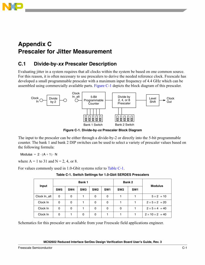
Appendix C Prescaler for Jitter Measurement
C.1 Divide-by-xx Prescaler DescriptionEvaluating jitter in a system requires that all clocks within the system be based on one common source. For this reason, it is often necessary to use prescalers to derive the needed reference clock. Freescale has developed a small programmable prescaler with a maximum input frequency of 4.4 GHz which can be assembled using commercially available parts. Figure C-1 depicts the block diagram of this prescaler.
Figure C-1. Divide-by-xx Prescaler Block Diagram
The input to the prescaler can be either through a divide-by-2 or directly into the 5-bit programmable counter. The bank 1 and bank 2 DIP switches can be used to select a variety of prescaler values based on the following formula:
where A = 1 to 31 and N = 2, 4, or 8.
For values commonly used in 1.0-Gbit systems refer to Table C-1.
Schematics for this prescaler are available from your Freescale field applications engineer.
Table C-1. Switch Settings for 1.0-Gbit SERDES Prescalers
InputBank 1 Bank 2
ModulusSW5 SW4 SW3 SW2 SW1 SW2 SW1
Clock In_alt 0 0 1 0 0 1 1 5 × 2 = 10
Clock In 0 0 1 0 0 1 1 2 × 5 × 2 = 20
Clock In 0 0 1 0 0 0 1 2 × 5 × 4 = 40
Clock In 0 1 0 0 1 1 1 2 × 10 × 2 = 40
Divideby 2
Bank 1 Switch
2, 4, or 8Divide by
Prescaler
5-BitProgrammable
Counter
Bank 2 Switch
LevelShift
ClockOut
ClockIn
ClockIn_alt
Modulus 2 A 1+( ) N⋅ ⋅=
Prescaler for Jitter Measurement
MC92602 Reduced Interface SerDes Design Verification Board User’s Guide, Rev. 3
C-2 Freescale Semiconductor
C.2 Prescaler ComponentsTable C-2 lists the major integrated circuit components needed for the prescaler.
Table C-2. Major Components for Divide-by-xx Prescaler
Part No. Manufacturer Supplier Comments
MC12093 Freescale Newark 1.1-GHz prescaler (divide by 2, 4, or 8)
MC100ELT23 On Semiconductor Newark Dual differential PECL to TTL translator, with separate inputs.
MC100ELT21 On Semiconductor Newark Single differential PECL to TTL translator.Alternative to above part.
MC100ELT26 On Semiconductor Newark Dual differential PECL to TTL translator, with common inputs. Alternative to above part.
HMMC-3122 Agilent Arrow 12-GHz divide-by-2 prescaler, GaAs HBT MMIC.
HMC364S8G Hittite Microwave Hittite 12-GHz divide-by-2 prescaler, GaAs HBT MMIC. Pin-for-pin alternative to above part.
HMC394LP4 Hittite Microwave Hittite 2.2-GHz programmable 5-bit counter, GaAs HBT MMIC.
MC92602 Reduced Interface SerDes Design Verification Board User’s Guide, Rev. 3
Freescale Semiconductor D-1
Appendix D Revision HistoryThis appendix provides a list of the major differences between revisions of the MC92602 Reduced Interface SerDes Design Verification Board Users Guide (MC92602DVBUG).
Table D-1 provides a revision history for this document.Table D-1. MC92602DVB Revision History
Rev. No. Date Substantive Change(s)
1 5/30/2002 Initial release.
1.1 10/1/2002 Editorial corrections.Appendix A: Added note concerning loading of RECV_x_CLK.
2 2/2004 Reformatted for new release.
3 12/2004 Reformatted to Freescale with minor edits.Added note to Figure 2-1. Top Side Part Location Diagram.Corrected pin numbers in Table 3-4. Data-Eye Generation Parallel Input Biasing.

Revision History
MC92602 Reduced Interface SerDes Design Verification Board User’s Guide, Rev. 3
D-2 Freescale Semiconductor

BackCover
How to Reach Us:
Home Page:www.freescale.com
E-mail:[email protected]
USA/Europe or Locations Not Listed:Freescale SemiconductorTechnical Information Center, CH3701300 N. Alma School Road Chandler, Arizona 85224 +1-800-521-6274 or [email protected]
Europe, Middle East, and Africa:Freescale Halbleiter Deutschland GmbHTechnical Information CenterSchatzbogen 781829 Muenchen, Germany+44 1296 380 456 (English)+46 8 52200080 (English)+49 89 92103 559 (German)+33 1 69 35 48 48 (French)[email protected]
Japan:Freescale Semiconductor Japan Ltd. Headquarters ARCO Tower 15F 1-8-1, Shimo-Meguro, Meguro-ku, Tokyo 153-0064 Japan 0120 191014 or +81 3 5437 [email protected]
Asia/Pacific:Freescale Semiconductor Hong Kong Ltd.Technical Information Center 2 Dai King Street Tai Po Industrial Estate Tai Po, N.T., Hong Kong +800 2666 [email protected]
For Literature Requests Only:Freescale Semiconductor Literature Distribution CenterP.O. Box 5405Denver, Colorado 802171-800-441-2447 or 303-675-2140Fax: [email protected]
Information in this document is provided solely to enable system and software implementers to use Freescale Semiconductor products. There are no express or implied copyright licenses granted hereunder to design or fabricate any integrated circuits or integrated circuits based on the information in this document.
Freescale Semiconductor reserves the right to make changes without further notice to any products herein. Freescale Semiconductor makes no warranty, representation or guarantee regarding the suitability of its products for any particular purpose, nor does Freescale Semiconductor assume any liability arising out of the application or use of any product or circuit, and specifically disclaims any and all liability, including without limitation consequential or incidental damages. “Typical” parameters that may be provided in Freescale Semiconductor data sheets and/or specifications can and do vary in different applications and actual performance may vary over time. All operating parameters, including “Typicals”, must be validated for each customer application by customer’s technical experts. Freescale Semiconductor does not convey any license under its patent rights nor the rights of others. Freescale Semiconductor products are not designed, intended, or authorized for use as components in systems intended for surgical implant into the body, or other applications intended to support or sustain life, or for any other application in which the failure of the Freescale Semiconductor product could create a situation where personal injury or death may occur. Should Buyer purchase or use Freescale Semiconductor products for any such unintended or unauthorized application, Buyer shall indemnify and hold Freescale Semiconductor and its officers, employees, subsidiaries, affiliates, and distributors harmless against all claims, costs, damages, and expenses, and reasonable attorney fees arising out of, directly or indirectly, any claim of personal injury or death associated with such unintended or unauthorized use, even if such claim alleges that Freescale Semiconductor was negligent regarding the design or manufacture of the part.
Freescale™ and the Freescale logo are trademarks of Freescale Semiconductor, Inc. All other product or service names are the property of their respective owners.
© Freescale Semiconductor, Inc. 2005. All rights reserved.
MC92602DVBUGRev. 3, 06/2005