Embed Size (px)
Citation preview
ABOV SEMICONDUCTOR Co., Ltd. LIGHT-TO-DIGITAL CONVERTER
MC8121
Data Sheet (REV.1.7)

MC8121
2 Jan 2015 REV1.7
REVISION HISTORY REVISION 0.0 (June 7, 2012)
- Initial Version
REVISION 0.1 (July 4, 2012) - Combine MC8111 & MC8121
- Correct register description
REVISION 0.2 (August 6, 2012)
- Add Optical characteristics
REVISION 1.0 (September 24, 2012)
- Change I2C slave address
- Change default values of registers
REVISION 1.1 (October 11, 2012)
- Add characteristics of CH1 PD
REVISION 1.2 (October 18, 2012) - Add Pinout & Package Dimension
REVISION 1.3 (November 06, 2012)
- Fix ODFN Package Dimension
- Correct device name for MC8121FN
REVISION 1.4 (January 15, 2013)
- Remove MC8111 related contents
REVISION 1.5 (January 22, 2013)
- Fix ID register description
REVISION 1.6 (March 08, 2013)
- Fix electrical characteristics
REVISION 1.61 (May 24, 2013)
- Correct unit notation
REVISION 1.62 (September 3, 2014)
- ATIME0, ATIME1, WTIME ‘11111111’ values are modified from 4608ms to 4590ms
MC8121
Jan 2015 REV1.7 3
REVISION 1.7 (January 16, 2015) - Correct spectral response
REVISION 1.7 Published by Design Team 2015 ABOV Semiconductor Co., Ltd. All rights reserved.
Additional information of this manual may be served by ABOV Semiconductor offices in Korea or Distributors. ABOV Semiconductor reserves the right to make changes to any information here in at any time without notice. The information, diagrams and other data in this manual are correct and reliable; however, ABOV Semiconductor is in no way responsible for any violations of patents or other rights of the third party generated by the use of this manual.
MC8121
4 Jan 2015 REV1.7
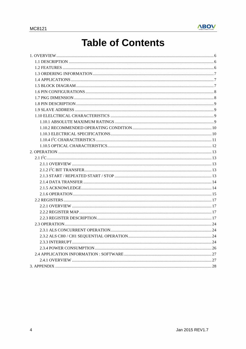
Table of Contents 1. OVERVIEW ....................................................................................................................................................... 6
1.1 DESCRIPTION ........................................................................................................................................... 6 1.2 FEATURES ................................................................................................................................................. 6 1.3 ORDERING INFORMATION .................................................................................................................... 7 1.4 APPLICATIONS ......................................................................................................................................... 7 1.5 BLOCK DIAGRAM .................................................................................................................................... 7 1.6 PIN CONFIGURATIONS ........................................................................................................................... 8 1.7 PKG DIMENSION ...................................................................................................................................... 8 1.8 PIN DESCRIPTION .................................................................................................................................... 9 1.9 SLAVE ADDRESS ..................................................................................................................................... 9 1.10 ELELCTRICAL CHARACTERISTICS ................................................................................................... 9
1.10.1 ABSOLUTE MAXIMUM RATINGS ............................................................................................... 9 1.10.2 RECOMMENDED OPERATING CONDITION ............................................................................ 10 1.10.3 ELECTRICAL SPECIFICATIONS ................................................................................................. 10 1.10.4 I2C CHARACTERISTICS ............................................................................................................... 11 1.10.5 OPTICAL CHARACTERISTICS .................................................................................................... 12
2. OPERATION ................................................................................................................................................... 13 2.1 I2C .............................................................................................................................................................. 13
2.1.1 OVERVIEW ...................................................................................................................................... 13 2.1.2 I2C BIT TRANSFER .......................................................................................................................... 13 2.1.3 START / REPEATED START / STOP ............................................................................................. 13 2.1.4 DATA TRANSFER ........................................................................................................................... 14 2.1.5 ACKNOWLEDGE ............................................................................................................................. 14 2.1.6 OPERATION ..................................................................................................................................... 15
2.2 REGISTERS .............................................................................................................................................. 17 2.2.1 OVERVIEW ...................................................................................................................................... 17 2.2.2 REGISTER MAP ............................................................................................................................... 17 2.2.3 REGISTER DESCRIPTION .............................................................................................................. 17
2.3 OPERATION ............................................................................................................................................. 24 2.3.1 ALS CONCURRENT OPERATION ................................................................................................. 24 2.3.2 ALS CH0 / CH1 SEQUENTIAL OPERATION ................................................................................ 24 2.3.3 INTERRUPT ...................................................................................................................................... 24 2.3.4 POWER CONSUMPTION ................................................................................................................ 26
2.4 APPLICATION INFORMATION : SOFTWARE .................................................................................... 27 2.4.1 OVERVIEW ...................................................................................................................................... 27
3. APPENDIX ...................................................................................................................................................... 28
MC8121
Jan 2015 REV1.7 5
List of Figures Figure 1-1 Block Diagram of MC8121 ................................................................................................... 7
Figure 1-2 Pinout – ODFN 2X2 6L(COL).............................................................................................. 8
Figure 1-3 Package Dimension – ODFN 2X2 6L(COL) ........................................................................ 8
Figure 1-4 Definition of ti rity ming for fast mode devices on the I2C bus .......................................... 11 Figure 1-5 Spectral response of MC8121 ............................................................................................. 12 Figure 2-1 Bit Transfer on the I2C-Bus ................................................................................................. 13 Figure 2-2 START and STOP Condition .............................................................................................. 14 Figure 2-3 STOP or Repeated START Condition ................................................................................ 14 Figure 2-4 Acknowledge on the I2C-Bus .............................................................................................. 15 Figure 2-5 I2C Write Protocol .............................................................................................................. 16 Figure 2-6 I2C Read Protocol ............................................................................................................... 16 Figure 2-7 ALS Operation .................................................................................................................... 24 Figure 2-8 ALS CH0 / CH1 Sequential Operation ............................................................................... 24 Figure 2-9 ALS CH0 Interrupt output (level or pulse interrupt) ........................................................... 25 Figure 2-10 ALS Interrupt Output (APER=1 or 2 & INTEDGE=0) .................................................... 25 Figure 2-11 Operating Modes ............................................................................................................... 27 Figure 3-1 Hardware pin connection diagram ...................................................................................... 28 Figure 3-2 I2C write example ............................................................................................................... 29 Figure 3-3 I2C read example ................................................................................................................ 29
MC8121
6 Jan 2015 REV1.7
MC8121
Digital Ambient Light Sensor
1. OVERVIEW
1.1 DESCRIPTION
The MC8121 is an advanced digital ambient light sensor (ALS) IC that transforms illuminance (light intensity) to a digital signal output. For ambient light sensing, MC8121 has two opened photodiodes(CH0/CH1). One is an whole ray responding photodiode and the other is a visible ray responding photodiode. The visible ray responding photodiode is coated with Infra Red cut off filter on a CMOS integrated circuit. The photovoltaic responses are converted into digital counter values by two internal ALS ADCs of 16-bit resolution. It closely approximates the human eye spectral response of visible wavelength. The operation voltage ranges from 2.4 to 3.6 volt.
The ALS features are ideal for reducing power consumption and adjusting brightness of display equipments like LCD, PDP, LED, virtual keyboard and portable projector, etc.
1.2 FEATURES
CMOS technology Independently programmable exposure time for ALS CH0 and CH1 ADCs Ambient Light Sensing Convert incident light intensity to digital data 16-bit ALS ADC resolution Automatic light flickering cancellation supporting Block off IR(Infrared) by IR cut off filter coating(CH0) Spectral response close to human eye Linear ALS response for easy design Low dark noise Additional Features I2C protocol interface Low stand-by current, 1uA typical Operating range 2.4 ~ 3.6V

MC8121
Jan 2015 REV1.7 7
1.3 ORDERING INFORMATION
DEVICE NAME PACKAGE−LEADS CH0 CH1
MC8121 chip sale IR cut off filter on wafer Visible + IR ray
MC8121FN ODFN 6L IR cut off filter on wafer Visible + IR ray
Table 1-1 Ordering Information
1.4 APPLICATIONS
Cell phone Display-equipped portable devices,etc..
1.5 BLOCK DIAGRAM
ALS CH0 ADC
ADC Counter
COMMAND CONTROL
INTERRUPT
I2C I/F
OSC 690kHz Timing Controller
ALS CH1 ADC
DATA REGISTER
SCL
SDA
ADDR DECODE
ADDR
VDD VSS
INT
CH0 : Visible ray
CH1 : Visible + IR ray
MEMORY (OTP)
for calibration
VPP
Figure 1-1 Block Diagram of MC8121
MC8121
8 Jan 2015 REV1.7
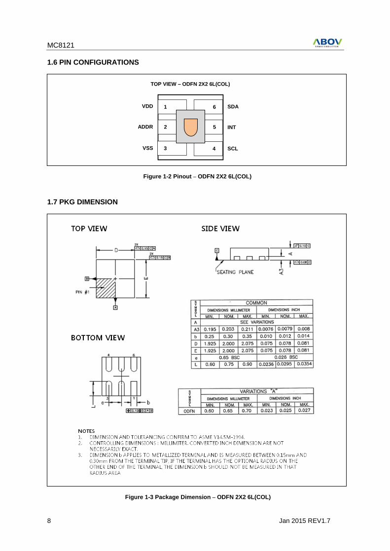
1.6 PIN CONFIGURATIONS
1.7 PKG DIMENSION
INT
1 SDA
SCL VSS
ADDR
VDD
TOP VIEW – ODFN 2X2 6L(COL)
2
3
6
5
4
Figure 1-3 Package Dimension – ODFN 2X2 6L(COL)
Figure 1-2 Pinout – ODFN 2X2 6L(COL)
MC8121
Jan 2015 REV1.7 9
1.8 PIN DESCRIPTION
PIN Number PIN Name Description I/O
1 VDD Power supply : 2.4 to 3.6V Power
2 ADDR Address Select Input
3 VSS Ground Power
4 SCL I2C Serial Clock Line Input
5 INT ALS Interrupt O(Open Drain)
6 SDA I2C Serial Data Line O(Open Drain)
Table 1-2 Pin Description – ODFN 2X2 6L(COL)
1.9 SLAVE ADDRESS
ADDR SLAVE ADDRESS
LOW / OPEN 0101_001
HIGH 1010_110
Table 1-3 Slave Address Selection
1.10 ELELCTRICAL CHARACTERISTICS
1.10.1 ABSOLUTE MAXIMUM RATINGS
Symbol Parameter Min. Max. Unit. Remark
VDD Supply voltage 0 4.0 V
Tstg Storage temperature range -40 85 ˚C
VO Digital ouput voltage range -0.5 4.0 V
IO Digital output current -1 20 mA
VHBM ESD tolerance, Human Body Model
8,000 V
Table 1-4 Absolute Maximum Ratings NOTE Stresses beyond those listed under “Absolute Maximum Ratings” may cause permanent damage to the device. This is a stress rating only and functional operation of the device at any other conditions beyond those indicated in the operational sections of this specification is not implied. Exposure to absolute maximum rating conditions for extended periods may affect device reliablility.

MC8121
10 Jan 2015 REV1.7
1.10.2 RECOMMENDED OPERATING CONDITION
Symbol Parameter Min. Typ. Max. Unit Remark
VDD Supply voltage 2.4 3.0 3.6 V
TA Operating temperature -40
85 ˚C
VIL SCL,SDA input low voltage
600 mV
VIH SCL,SDA input low voltage 1.4
V
Table 1-5 Recommended Operating Condition
1.10.3 ELECTRICAL SPECIFICATIONS
(VDD =3.0V, VSS =0V, TA=+25℃±10%)
Symbol Parameter Min. Typ. Max. Unit Remark VDD Power Supply 2.4 - 3.6 V
ISLEEP Stand-by Current 1 3 uA I2C interface enable IDDALS0 Active Current for ALS CH0 80 uA IDDALS1 Active Current for ALS CH1 80 uA
IDDALS01 Active Current for ALS CH0 and CH1 120 uA
λPCH0 Peak Sensitivity wavelength of ALS CH0 550 nm
λPCH1 Peak Sensitivity wavelength of ALS CH1 850 nm
fOSC Internal Oscillator Frequency 552 690 828 kHz
tINT ADC Integration/Conversion Time 100 500 ms 16-bit ADC data
VOL INT,SDA ouput low voltage 0 0.4 V 6mA sink current A0000L ADC Count Value of CH0
PD (ATIME0 = 06H, INTR[7]=1)
- 0 2 counts @0Lux, white color LED A0001L 5 counts @1Lux, white color LED A0200L 980 1090 1200 counts @200Lux, white color LED A1000L ADC Count Value of CH1
PD (ATIME0 = 06H, INTR[7]=1)
- 0 4 counts @0Lux, white color LED A1001L 8 counts @1Lux, white color LED A1200L 1334 1640 1975 counts @200Lux, white color LED
DFALS0 Full Scale ALS CH0 ADC Count 65535 counts
DFALS1 Full Scale ALS CH1 ADC Count 65535 counts
Table 1-6 Electrical Specifications
MC8121
Jan 2015 REV1.7 11
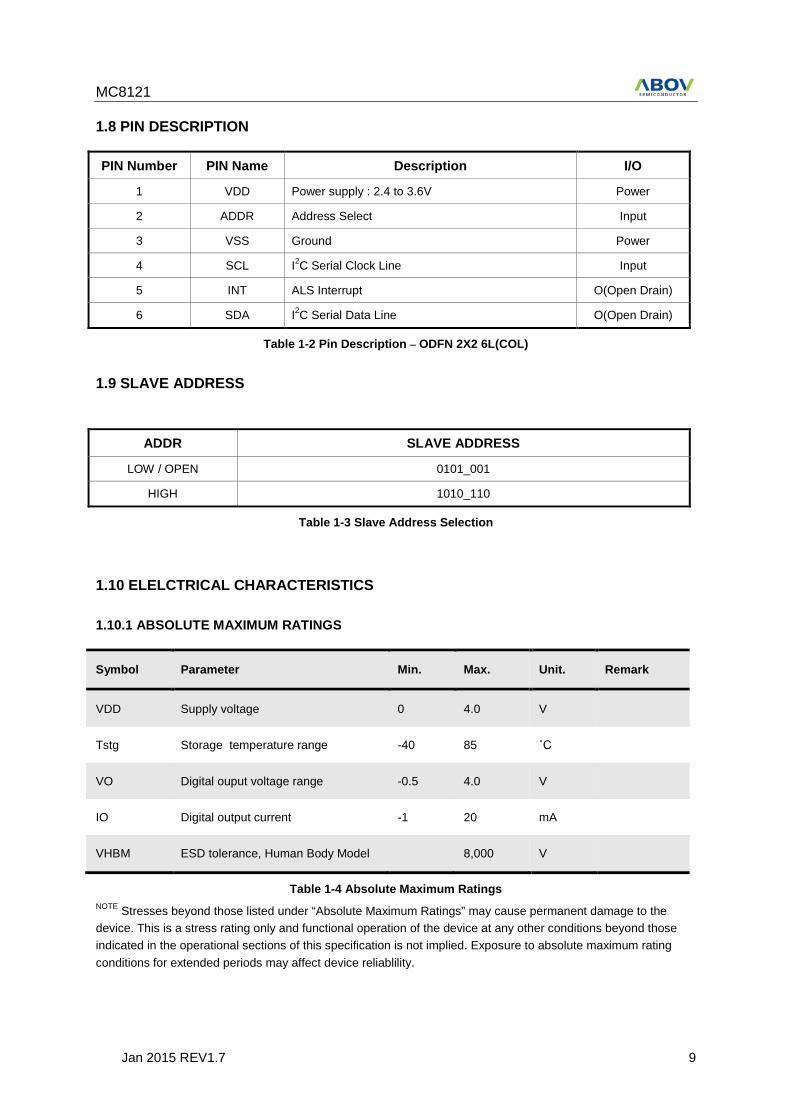
1.10.4 I2C CHARACTERISTICS
The following table and figure show the timing codition of SDA and SCL bus lines for fast mode I2C bus devices. NOTE1.
(VDD =3.0V, VSS =0V, TA=+25℃±10%)
Parameter SymbolNOTE2 Min Max Unit SCL clock frequency fSCL 0 400 kHz Hold time after (repeated) START condition. After this period, the first clock pulse is generated tHD;STA 0.6 - us
LOW period of the SCL clock tLOW 1.3 - us HIGH period of the SCL clock tHIGH 0.6 - us Setup time for a repeated START condition tSU;STA 0.6 - us Data hold time tHD;DAT 0 0.9 us Data setup time tSU;DAT 100 - ns Clock/data fall time tF 0 300 ns Clock/data rise time tR 0 300 ns Setup time for STOP condition tSU;STO 0.6 - us Bus free time between a STOP and START condtion tBUF 1.3 - us
Table 1-7 Timing characteristics of I2C
NOTE1 All timing is shown with respect to 30% VDD and 70% VDD.
SDA
SCL
tLOW
tF
tHD;STA
tR
tHD;DAT
tSU;DAT
tHIGH
tF
tSU;STA
tHD;DAT tBUF tR
tSU;STO
S Sr S P
Figure 1-4 Definition of ti rity ming for fast mode devices on the I2C bus
MC8121
12 Jan 2015 REV1.7
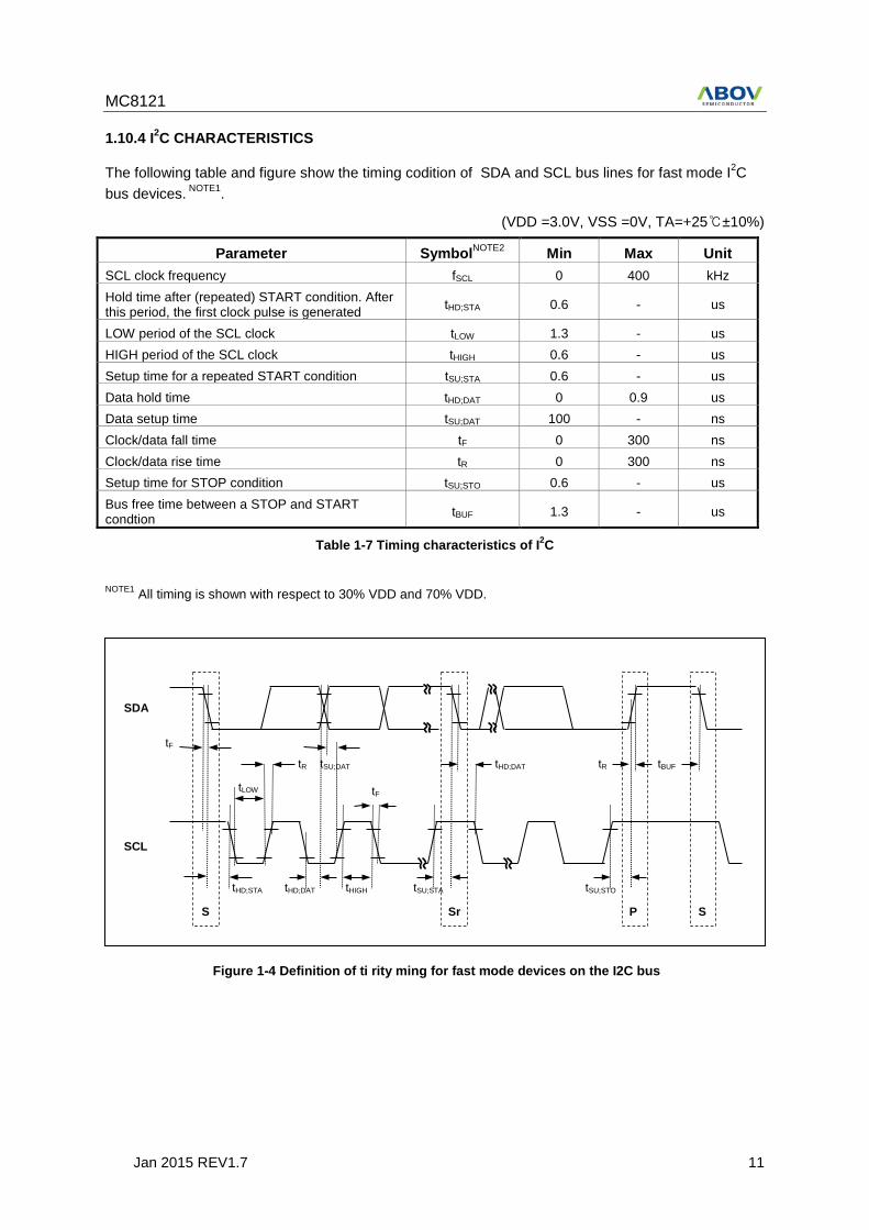
1.10.5 OPTICAL CHARACTERISTICS
A. Spectral response Spectrum of MC8121 is the below curve by using monochrometer and integrated sphere.
Figure 1-5 Spectral response of MC8121
MC8121
Jan 2015 REV1.7 13
2. OPERATION
2.1 I2C
2.1.1 OVERVIEW
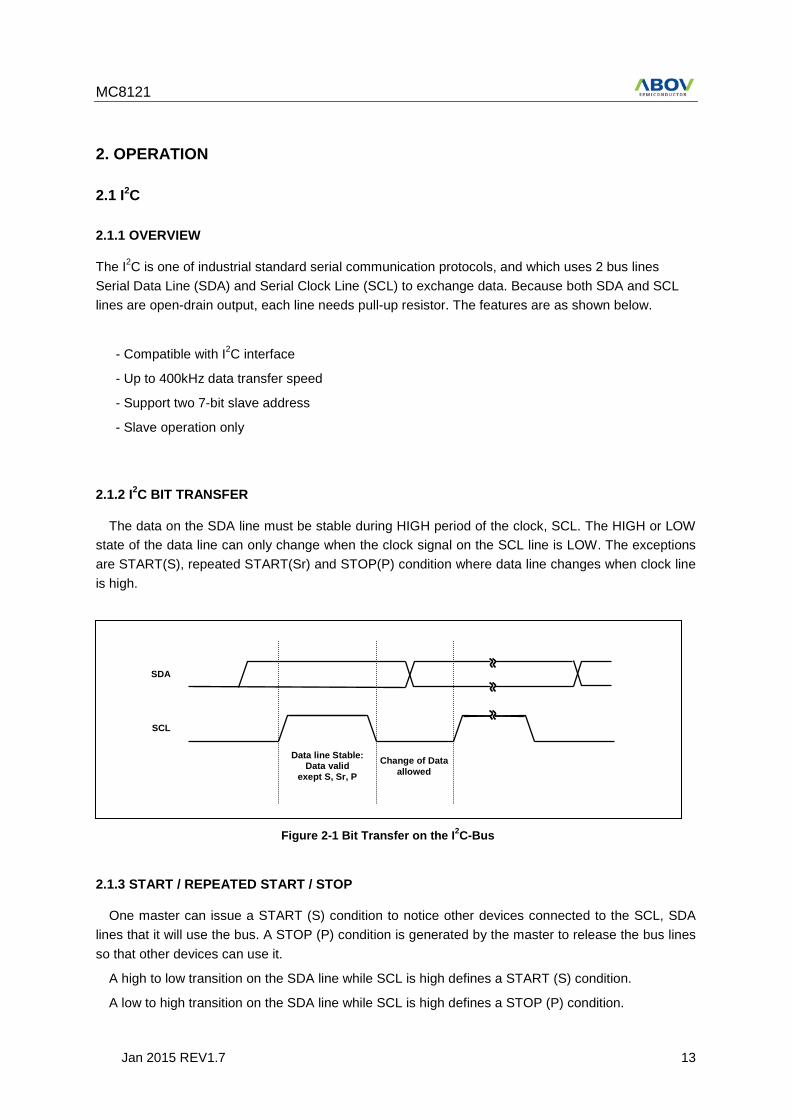
The I2C is one of industrial standard serial communication protocols, and which uses 2 bus lines Serial Data Line (SDA) and Serial Clock Line (SCL) to exchange data. Because both SDA and SCL lines are open-drain output, each line needs pull-up resistor. The features are as shown below.
- Compatible with I2C interface
- Up to 400kHz data transfer speed
- Support two 7-bit slave address
- Slave operation only
2.1.2 I2C BIT TRANSFER
The data on the SDA line must be stable during HIGH period of the clock, SCL. The HIGH or LOW state of the data line can only change when the clock signal on the SCL line is LOW. The exceptions are START(S), repeated START(Sr) and STOP(P) condition where data line changes when clock line is high.
2.1.3 START / REPEATED START / STOP
One master can issue a START (S) condition to notice other devices connected to the SCL, SDA lines that it will use the bus. A STOP (P) condition is generated by the master to release the bus lines so that other devices can use it.
A high to low transition on the SDA line while SCL is high defines a START (S) condition.
A low to high transition on the SDA line while SCL is high defines a STOP (P) condition.
SCL
SDA
Data line Stable: Data valid
exept S, Sr, P Change of Data
allowed
Figure 2-1 Bit Transfer on the I2C-Bus
MC8121
14 Jan 2015 REV1.7
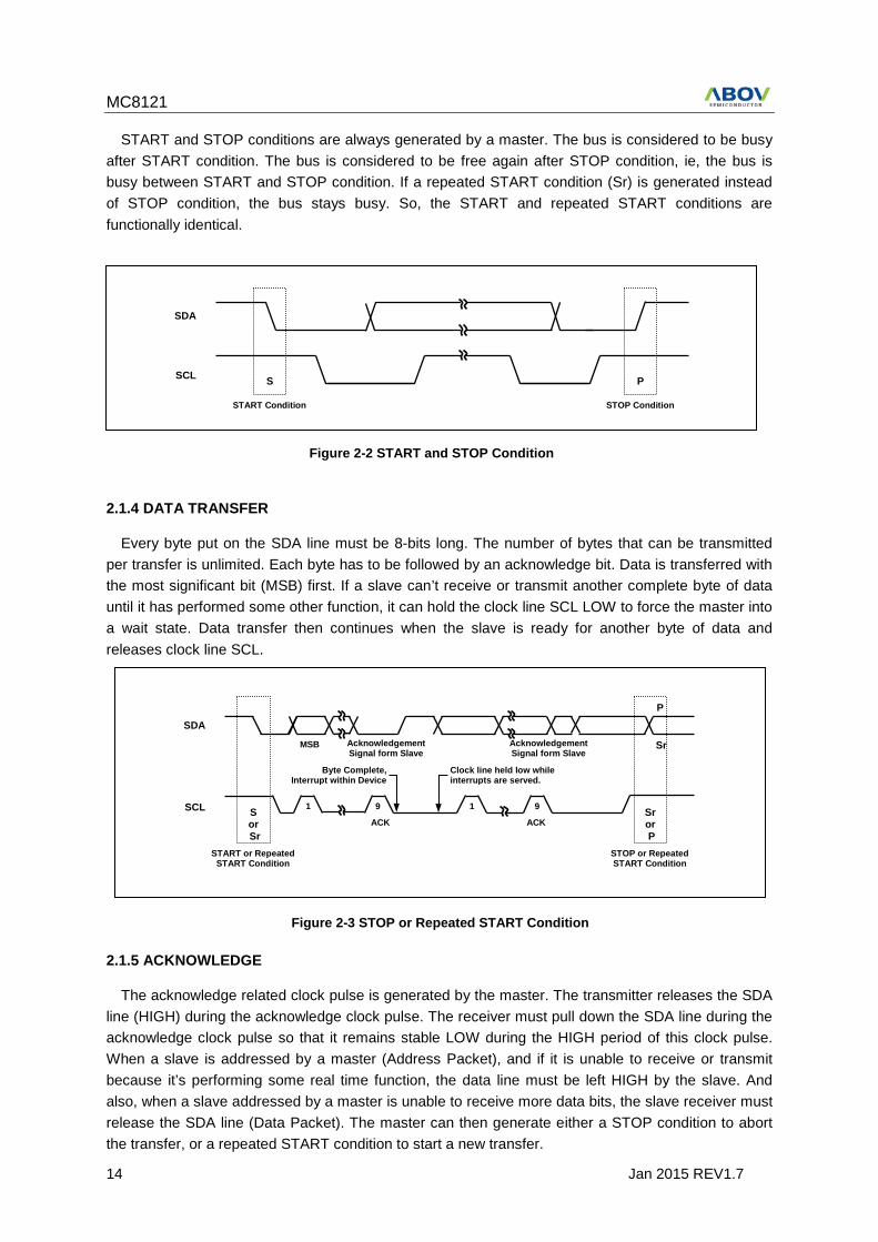
START and STOP conditions are always generated by a master. The bus is considered to be busy after START condition. The bus is considered to be free again after STOP condition, ie, the bus is busy between START and STOP condition. If a repeated START condition (Sr) is generated instead of STOP condition, the bus stays busy. So, the START and repeated START conditions are functionally identical.
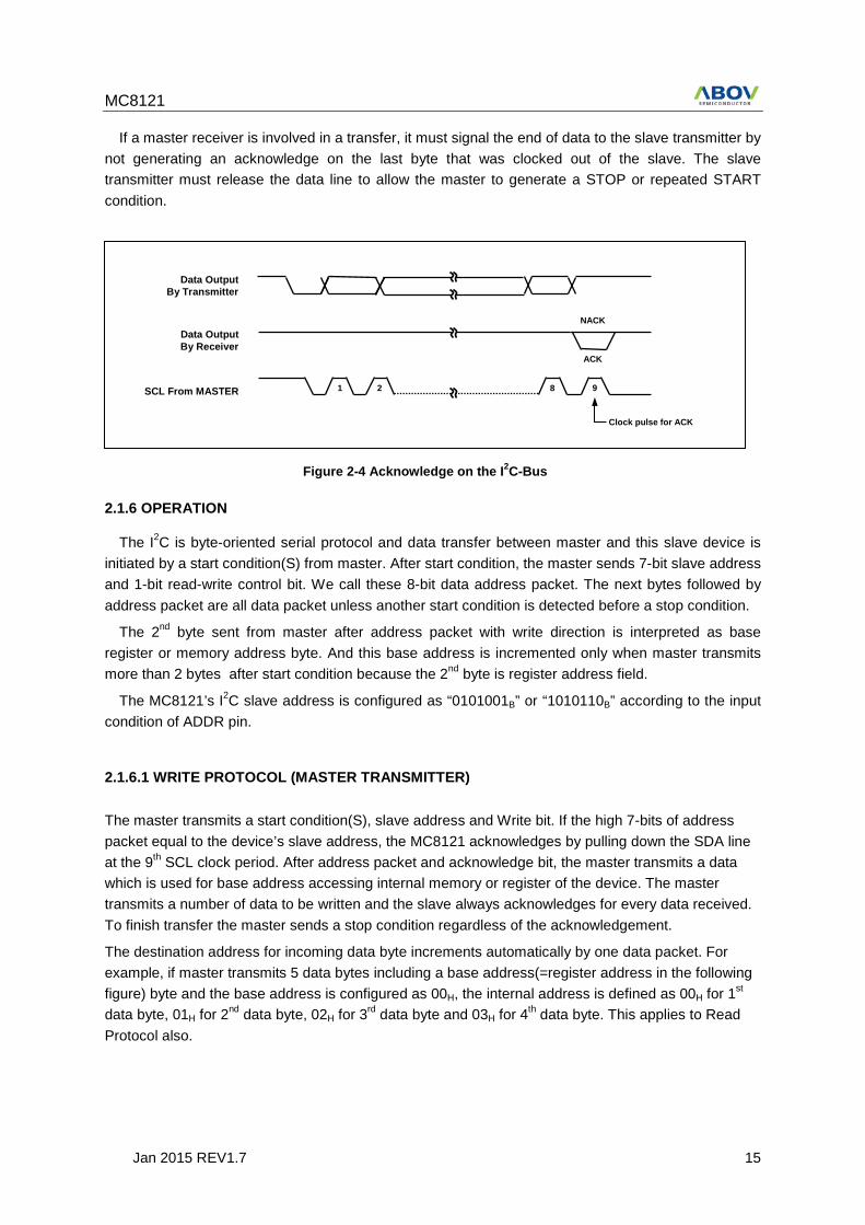
2.1.4 DATA TRANSFER
Every byte put on the SDA line must be 8-bits long. The number of bytes that can be transmitted per transfer is unlimited. Each byte has to be followed by an acknowledge bit. Data is transferred with the most significant bit (MSB) first. If a slave can’t receive or transmit another complete byte of data until it has performed some other function, it can hold the clock line SCL LOW to force the master into a wait state. Data transfer then continues when the slave is ready for another byte of data and releases clock line SCL.
2.1.5 ACKNOWLEDGE
The acknowledge related clock pulse is generated by the master. The transmitter releases the SDA line (HIGH) during the acknowledge clock pulse. The receiver must pull down the SDA line during the acknowledge clock pulse so that it remains stable LOW during the HIGH period of this clock pulse. When a slave is addressed by a master (Address Packet), and if it is unable to receive or transmit because it’s performing some real time function, the data line must be left HIGH by the slave. And also, when a slave addressed by a master is unable to receive more data bits, the slave receiver must release the SDA line (Data Packet). The master can then generate either a STOP condition to abort the transfer, or a repeated START condition to start a new transfer.
SCL
SDA
START Condition
S P
STOP Condition
START or Repeated START Condition
S or Sr
STOP or Repeated START Condition
Sr or P
MSB Acknowledgement Signal form Slave
Acknowledgement Signal form Slave
Byte Complete, Interrupt within Device
Clock line held low while interrupts are served.
1 9 1 9
ACK ACK
SDA
SCL
Sr
P
Figure 2-2 START and STOP Condition
Figure 2-3 STOP or Repeated START Condition
MC8121
Jan 2015 REV1.7 15
If a master receiver is involved in a transfer, it must signal the end of data to the slave transmitter by not generating an acknowledge on the last byte that was clocked out of the slave. The slave transmitter must release the data line to allow the master to generate a STOP or repeated START condition.
2.1.6 OPERATION
The I2C is byte-oriented serial protocol and data transfer between master and this slave device is initiated by a start condition(S) from master. After start condition, the master sends 7-bit slave address and 1-bit read-write control bit. We call these 8-bit data address packet. The next bytes followed by address packet are all data packet unless another start condition is detected before a stop condition.
The 2nd byte sent from master after address packet with write direction is interpreted as base register or memory address byte. And this base address is incremented only when master transmits more than 2 bytes after start condition because the 2nd byte is register address field.
The MC8121’s I2C slave address is configured as “0101001B” or “1010110B” according to the input condition of ADDR pin.
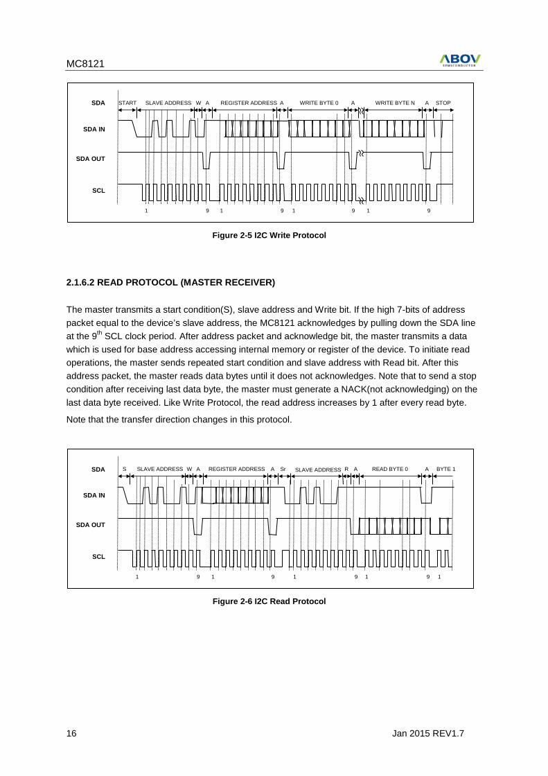
2.1.6.1 WRITE PROTOCOL (MASTER TRANSMITTER)
The master transmits a start condition(S), slave address and Write bit. If the high 7-bits of address packet equal to the device’s slave address, the MC8121 acknowledges by pulling down the SDA line at the 9th SCL clock period. After address packet and acknowledge bit, the master transmits a data which is used for base address accessing internal memory or register of the device. The master transmits a number of data to be written and the slave always acknowledges for every data received. To finish transfer the master sends a stop condition regardless of the acknowledgement.
The destination address for incoming data byte increments automatically by one data packet. For example, if master transmits 5 data bytes including a base address(=register address in the following figure) byte and the base address is configured as 00H, the internal address is defined as 00H for 1st data byte, 01H for 2nd data byte, 02H for 3rd data byte and 03H for 4th data byte. This applies to Read Protocol also.
1 2 8
Data Output By Transmitter
9
ACK
NACK
Clock pulse for ACK
Data Output By Receiver
SCL From MASTER
Figure 2-4 Acknowledge on the I2C-Bus
MC8121
16 Jan 2015 REV1.7
2.1.6.2 READ PROTOCOL (MASTER RECEIVER)
The master transmits a start condition(S), slave address and Write bit. If the high 7-bits of address packet equal to the device’s slave address, the MC8121 acknowledges by pulling down the SDA line at the 9th SCL clock period. After address packet and acknowledge bit, the master transmits a data which is used for base address accessing internal memory or register of the device. To initiate read operations, the master sends repeated start condition and slave address with Read bit. After this address packet, the master reads data bytes until it does not acknowledges. Note that to send a stop condition after receiving last data byte, the master must generate a NACK(not acknowledging) on the last data byte received. Like Write Protocol, the read address increases by 1 after every read byte.
Note that the transfer direction changes in this protocol.
SDA
SDA IN
SCL
START
9 9
SDA OUT
SLAVE ADDRESS W A REGISTER ADDRESS A WRITE BYTE 0 STOP A A WRITE BYTE N
9 9 1 1 1 1
SDA
SDA IN
SCL
S
9 9
SDA OUT
SLAVE ADDRESS W A REGISTER ADDRESS A Sr
9 9
A SLAVE ADDRESS READ BYTE 0 A BYTE 1
1 1 1 1 1
R
Figure 2-5 I2C Write Protocol
Figure 2-6 I2C Read Protocol
MC8121
Jan 2015 REV1.7 17
2.2 REGISTERS
2.2.1 OVERVIEW
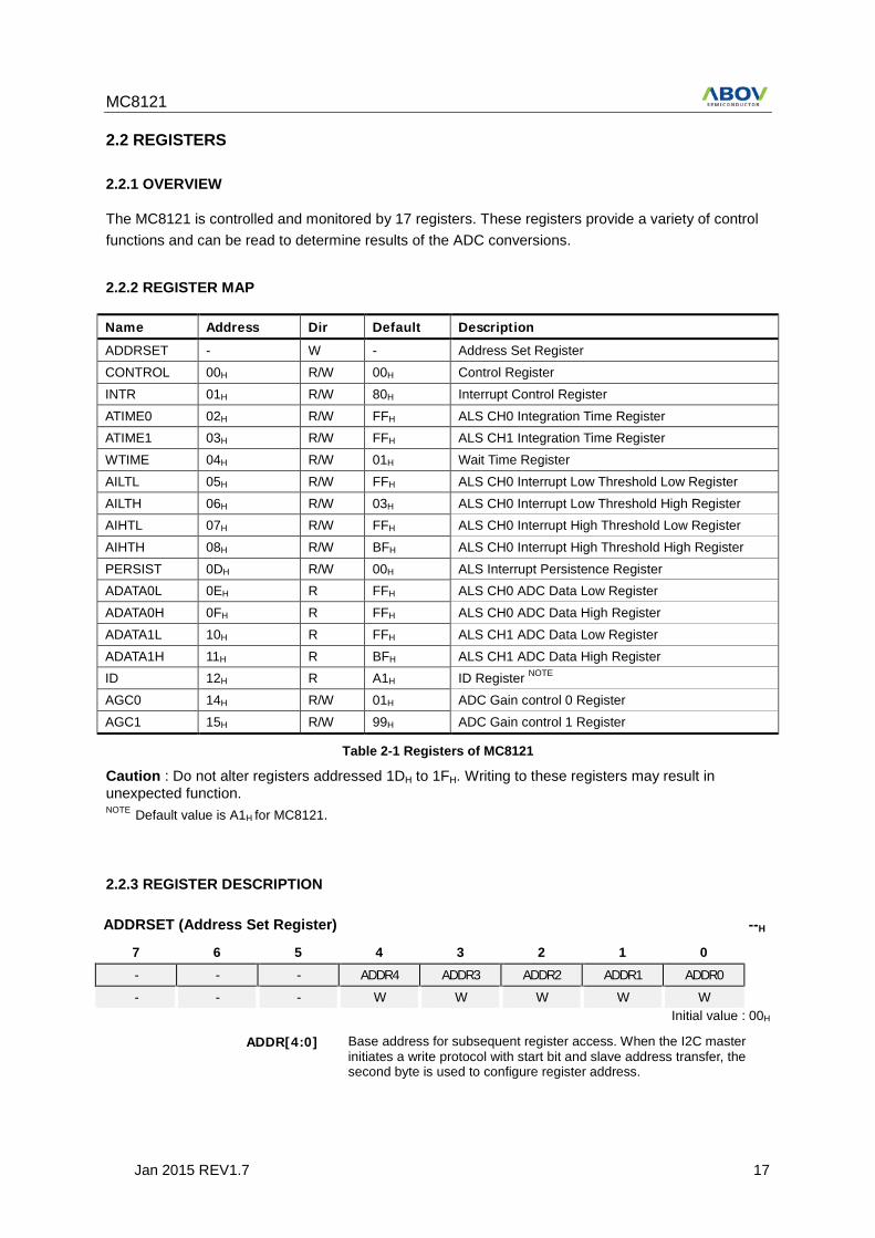
The MC8121 is controlled and monitored by 17 registers. These registers provide a variety of control functions and can be read to determine results of the ADC conversions.
2.2.2 REGISTER MAP
Name Address Dir Default Description
ADDRSET - W - Address Set Register CONTROL 00H R/W 00H Control Register INTR 01H R/W 80H Interrupt Control Register ATIME0 02H R/W FFH ALS CH0 Integration Time Register ATIME1 03H R/W FFH ALS CH1 Integration Time Register WTIME 04H R/W 01H Wait Time Register AILTL 05H R/W FFH ALS CH0 Interrupt Low Threshold Low Register AILTH 06H R/W 03H ALS CH0 Interrupt Low Threshold High Register AIHTL 07H R/W FFH ALS CH0 Interrupt High Threshold Low Register AIHTH 08H R/W BFH ALS CH0 Interrupt High Threshold High Register PERSIST 0DH R/W 00H ALS Interrupt Persistence Register ADATA0L 0EH R FFH ALS CH0 ADC Data Low Register ADATA0H 0FH R FFH ALS CH0 ADC Data High Register ADATA1L 10H R FFH ALS CH1 ADC Data Low Register ADATA1H 11H R BFH ALS CH1 ADC Data High Register ID 12H R A1H ID Register NOTE AGC0 14H R/W 01H ADC Gain control 0 Register AGC1 15H R/W 99H ADC Gain control 1 Register
Table 2-1 Registers of MC8121
Caution : Do not alter registers addressed 1DH to 1FH. Writing to these registers may result in unexpected function. NOTE Default value is A1H for MC8121.
2.2.3 REGISTER DESCRIPTION
ADDRSET (Address Set Register) --H
7 6 5 4 3 2 1 0 - - - ADDR4 ADDR3 ADDR2 ADDR1 ADDR0
- - - W W W W W Initial value : 00H
ADDR[4:0] Base address for subsequent register access. When the I2C master initiates a write protocol with start bit and slave address transfer, the second byte is used to configure register address.
MC8121
18 Jan 2015 REV1.7
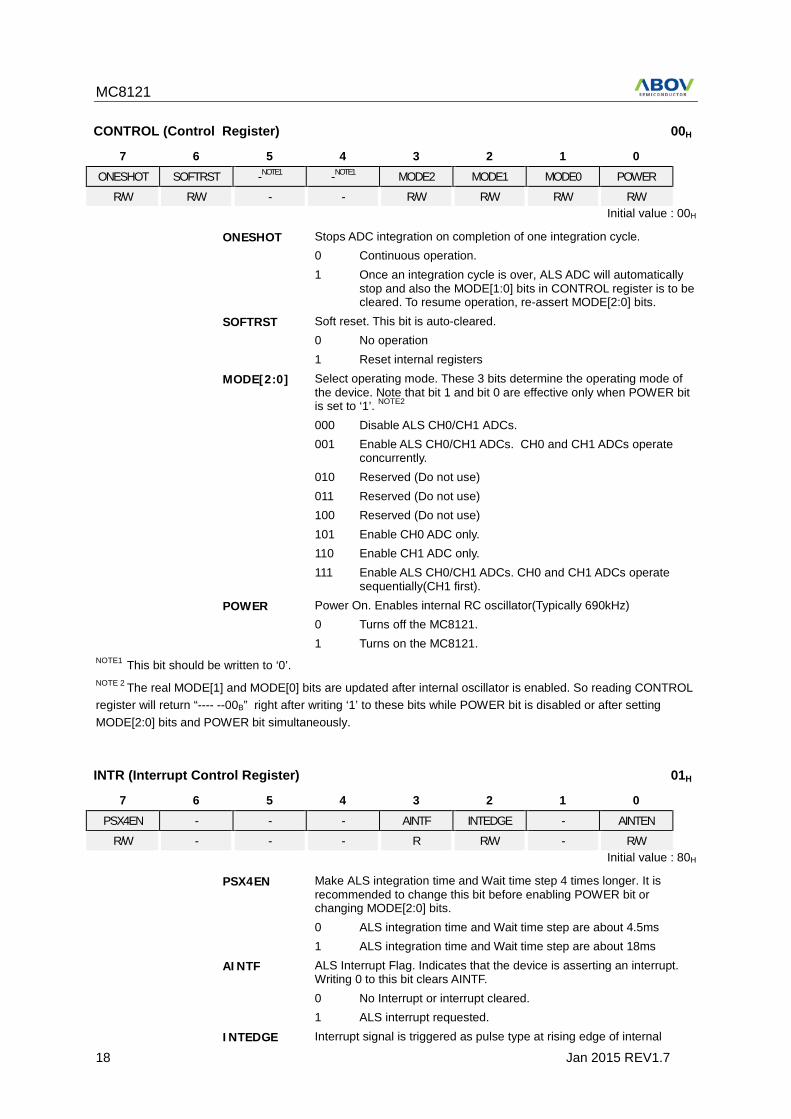
CONTROL (Control Register) 00H
7 6 5 4 3 2 1 0 ONESHOT SOFTRST - NOTE1 - NOTE1 MODE2 MODE1 MODE0 POWER
R/W R/W - - R/W R/W R/W R/W Initial value : 00H
ONESHOT Stops ADC integration on completion of one integration cycle. 0 Continuous operation. 1 Once an integration cycle is over, ALS ADC will automatically
stop and also the MODE[1:0] bits in CONTROL register is to be cleared. To resume operation, re-assert MODE[2:0] bits.
SOFTRST Soft reset. This bit is auto-cleared. 0 No operation 1 Reset internal registers
MODE[2:0] Select operating mode. These 3 bits determine the operating mode of the device. Note that bit 1 and bit 0 are effective only when POWER bit is set to ‘1’. NOTE2 000 Disable ALS CH0/CH1 ADCs. 001 Enable ALS CH0/CH1 ADCs. CH0 and CH1 ADCs operate
concurrently. 010 Reserved (Do not use) 011 Reserved (Do not use) 100 Reserved (Do not use) 101 Enable CH0 ADC only. 110 Enable CH1 ADC only. 111 Enable ALS CH0/CH1 ADCs. CH0 and CH1 ADCs operate
sequentially(CH1 first).
POWER Power On. Enables internal RC oscillator(Typically 690kHz) 0 Turns off the MC8121. 1 Turns on the MC8121.
NOTE1 This bit should be written to ‘0’.
NOTE 2 The real MODE[1] and MODE[0] bits are updated after internal oscillator is enabled. So reading CONTROL register will return “---- --00B” right after writing ‘1’ to these bits while POWER bit is disabled or after setting MODE[2:0] bits and POWER bit simultaneously.
INTR (Interrupt Control Register) 01H
7 6 5 4 3 2 1 0 PSX4EN - - - AINTF INTEDGE - AINTEN
R/W - - - R R/W - R/W Initial value : 80H
PSX4EN Make ALS integration time and Wait time step 4 times longer. It is recommended to change this bit before enabling POWER bit or changing MODE[2:0] bits. 0 ALS integration time and Wait time step are about 4.5ms 1 ALS integration time and Wait time step are about 18ms
AINTF ALS Interrupt Flag. Indicates that the device is asserting an interrupt. Writing 0 to this bit clears AINTF. 0 No Interrupt or interrupt cleared. 1 ALS interrupt requested.
INTEDGE Interrupt signal is triggered as pulse type at rising edge of internal
MC8121
Jan 2015 REV1.7 19
clock,typically 1.45us period. The host needs not to clear interrupt. 0 Level interrupt 1 Edge interrupt
AINTEN Enables ALS Interrupt generation. 0 ALS Interrupt output is disabled. 1 ALS Interrupt occurs on INT pin.
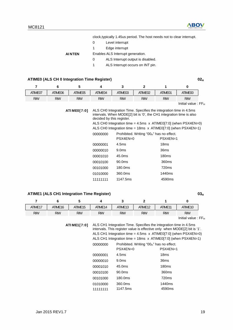
ATIME0 (ALS CH 0 Integration Time Register) 02H
7 6 5 4 3 2 1 0 ATIME07 ATIME06 ATIME05 ATIME04 ATIME03 ATIME02 ATIME01 ATIME00
R/W R/W R/W R/W R/W R/W R/W R/W Initial value : FFH
ATIME0[7:0] ALS CH0 Integration Time. Specifies the integration time in 4.5ms intervals. When MODE[2] bit is ‘0’, the CH1 integration time is also decided by this register. ALS CH0 Integration time = 4.5ms x ATIME0[7:0] (when PSX4EN=0) ALS CH0 Integration time = 18ms x ATIME0[7:0] (when PSX4EN=1)
00000000 Prohibited. Writing “00H” has no effect. PSX4EN=0 PSX4EN=1
00000001 4.5ms 18ms
00000010 9.0ms 36ms
00001010 45.0ms 180ms
00010100 90.0ms 360ms
00101000 180.0ms 720ms
01010000 360.0ms 1440ms
11111111 1147.5ms 4590ms
ATIME1 (ALS CH1 Integration Time Register) 03H
7 6 5 4 3 2 1 0 ATIME17 ATIME16 ATIME15 ATIME14 ATIME13 ATIME12 ATIME11 ATIME10
R/W R/W R/W R/W R/W R/W R/W R/W Initial value : FFH
ATIME1[7:0] ALS CH1 Integration Time. Specifies the integration time in 4.5ms intervals. This register value is effective only when MODE[2] bit is ‘1’. ALS CH1 Integration time = 4.5ms x ATIME0[7:0] (when PSX4EN=0) ALS CH1 Integration time = 18ms x ATIME0[7:0] (when PSX4EN=1)
00000000 Prohibited. Writing “00H” has no effect. PSX4EN=0 PSX4EN=1
00000001 4.5ms 18ms
00000010 9.0ms 36ms
00001010 45.0ms 180ms
00010100 90.0ms 360ms
00101000 180.0ms 720ms
01010000 11111111
360.0ms 1440ms 1147.5ms 4590ms
MC8121
20 Jan 2015 REV1.7
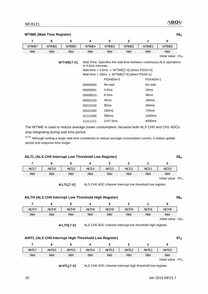
WTIME (Wait Time Register) 04H
7 6 5 4 3 2 1 0 WTIME7 WTIME6 WTIME5 WTIME4 WTIME3 WTIME2 WTIME1 WTIME0
R/W R/W R/W R/W R/W R/W R/W R/W Initial value : 01H
WTIME[7:0] Wait Time. Specifies the wait time between continuous ALS operations in 4.5ms intervals. Wait time = 4.5ms x WTIME[7:0] (when PSX4=0) Wait time = 18ms x WTIME[7:0] (when PSX4=1)
PSX4EN=0 PSX4EN=1
00000000 No wait No wait
00000001 4.5ms 18ms
00000010 9.0ms 36ms
00001010 45ms 180ms
00010100 90ms 360ms
00101000 180ms 720ms
01111000 360ms 1440ms
11111111 1147.5ms 4590ms
The WTIME is used to reduce average power consumption, because both ALS CH0 and CH1 ADCs stop integrating during wait time period. NOTE Although setting a larger wait time contributes to reduce average consumption current, it makes update period and response time longer.
AILTL (ALS CH0 Interrupt Low Threshold Low Register) 05H
7 6 5 4 3 2 1 0 AILTL7 AILTL6 AILTL5 AILTL4 AILTL3 AILTL2 AILTL1 AILTL0
R/W R/W R/W R/W R/W R/W R/W R/W Initial value : FFH
AILTL[7:0] ALS CH0 ADC channel interrupt low threshold low register.
AILTH (ALS CH0 Interrupt Low Threshold High Register) 06H
7 6 5 4 3 2 1 0 AILTH7 AILTH6 AILTH5 AILTH4 AILTH3 AILTH2 AILTH1 AILTH0
R/W R/W R/W R/W R/W R/W R/W R/W Initial value : 03H
AILTH[7:0] ALS CH0 ADC channel interrupt low threshold high register.
AIHTL (ALS CH0 Interrupt High Threshold Low Register) 07H
7 6 5 4 3 2 1 0 AIHTL7 AIHTL6 AIHTL5 AIHTL4 AIHTL3 AIHTL2 AIHTL1 AIHTL0
R/W R/W R/W R/W R/W R/W R/W R/W Initial value : FFH
AIHTL[7:0] ALS CH0 ADC channel interrupt high threshold low register.

MC8121
Jan 2015 REV1.7 21
AIHTH (ALS CH0 Interrupt High Threshold High Register) 08H
7 6 5 4 3 2 1 0 AIHTH7 AIHTH6 AIHTH5 AIHTH4 AIHTH3 AIHTH2 AIHTH1 AIHTH0
R/W R/W R/W R/W R/W R/W R/W R/W Initial value : BFH
AIHTH[7:0] ALS CH0 ADC channel interrupt high threshold high register.
The interrupt threshold registers store the values to be used as the high and low trigger points for the adc data registers. If the value of adc data register crosses below or equal to the low threshold specified, an interrupt can be asserted on the interrupt pin. Likewise, if the result from ADC conversion crosses above the high threshold specified, an interrupt can be asserted on the interrupt pin. The concatenated AILTH and AILTL is used as interrupt low threshold(=AILT) and the concatenated AIHTH and AIHTL is used as interrupt high threshold(=AIHT).
PERSIST (Interrupt Persistence Register) 0DH
7 6 5 4 3 2 1 0 - - - - APER3 APER2 APER1 APER0
- - - - R/W R/W R/W R/W Initial value : 00H
APER[3:0] ALS CH0 Interrupt persistence. These bit field control the rate of ALS interrupt request to host chip.
0000 Every ALS CH0 cycle generates an interrupt.
0001 1 consecutive ALS CH0 ADC value out of range.
0010 2 consecutive ALS CH0 ADC value out of range.
… …
1111 15 consecutive ALS CH0 ADC value out of range.
ADATA0L (ALS CH0 ADC Data Low Register) 0EH
7 6 5 4 3 2 1 0 ADATA0L7 ADATA0L6 ADATA0L5 ADATA0L4 ADATA0L3 ADATA0L2 ADATA0L1 ADATA0L0
R R R R R R R R Initial value : FFH
ADATA0L[7:0] ALS CH0 ADC data low register.
The ALS ADCs included in MC8121 are of 16-bit resolution, and the integrated values appear on two registers ADATA0L/ADATA0H and ADATA1L/ADATA1H respectively. All ALS ADC data registers are read-only.
MC8121
22 Jan 2015 REV1.7
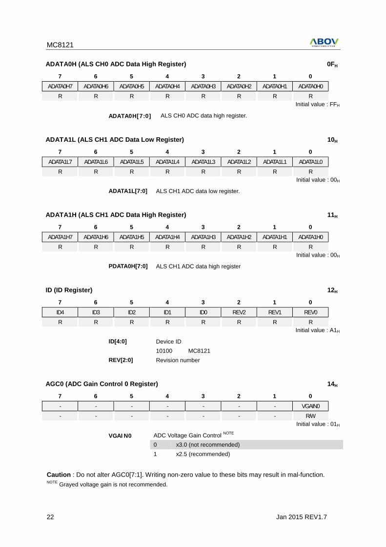
ADATA0H (ALS CH0 ADC Data High Register) 0FH
7 6 5 4 3 2 1 0 ADATA0H7 ADATA0H6 ADATA0H5 ADATA0H4 ADATA0H3 ADATA0H2 ADATA0H1 ADATA0H0
R R R R R R R R Initial value : FFH
ADATA0H[7:0] ALS CH0 ADC data high register.
ADATA1L (ALS CH1 ADC Data Low Register) 10H
7 6 5 4 3 2 1 0 ADATA1L7 ADATA1L6 ADATA1L5 ADATA1L4 ADATA1L3 ADATA1L2 ADATA1L1 ADATA1L0
R R R R R R R R Initial value : 00H
ADATA1L[7:0] ALS CH1 ADC data low register.
ADATA1H (ALS CH1 ADC Data High Register) 11H
7 6 5 4 3 2 1 0 ADATA1H7 ADATA1H6 ADATA1H5 ADATA1H4 ADATA1H3 ADATA1H2 ADATA1H1 ADATA1H0
R R R R R R R R Initial value : 00H
PDATA0H[7:0] ALS CH1 ADC data high register
ID (ID Register) 12H
7 6 5 4 3 2 1 0 ID4 ID3 ID2 ID1 ID0 REV2 REV1 REV0
R R R R R R R R Initial value : A1H
ID[4:0] Device ID 10100 MC8121
REV[2:0] Revision number
AGC0 (ADC Gain Control 0 Register) 14H
7 6 5 4 3 2 1 0 - - - - - - - VGAIN0
- - - - - - - R/W Initial value : 01H
VGAIN0 ADC Voltage Gain Control NOTE 0 x3.0 (not recommended) 1 x2.5 (recommended)
Caution : Do not alter AGC0[7:1]. Writing non-zero value to these bits may result in mal-function. NOTE Grayed voltage gain is not recommended.
MC8121
Jan 2015 REV1.7 23
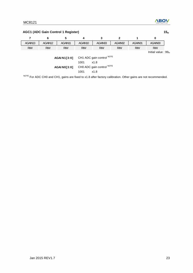
AGC1 (ADC Gain Control 1 Register) 15H
7 6 5 4 3 2 1 0 AGAIN13 AGAIN12 AGAIN11 AGAIN10 AGAIN03 AGAIN02 AGAIN01 AGAIN00
R/W R/W R/W R/W R/W R/W R/W R/W Initial value : 99H
AGAIN1[3:0] CH1 ADC gain control NOTE 1001 x1.8
AGAIN0[3:0] CH0 ADC gain control NOTE 1001 x1.8
NOTE For ADC CH0 and CH1, gains are fixed to x1.8 after factory calibration. Other gains are not recommended.
MC8121
24 Jan 2015 REV1.7
2.3 OPERATION
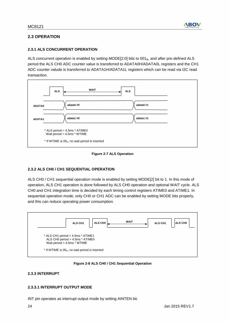
2.3.1 ALS CONCURRENT OPERATION
ALS concurrent operation is enabled by setting MODE[2:0] bits to 001B, and after pre-defined ALS period the ALS CH0 ADC counter value is transferred to ADATA0H/ADATA0L registers and the CH1 ADC counter valude is transferred to ADATA1H/ADATA1L registers which can be read via I2C read transaction.
2.3.2 ALS CH0 / CH1 SEQUENTIAL OPERATION
ALS CH0 / CH1 sequential operation mode is enabled by setting MODE[2] bit to 1. In this mode of operation, ALS CH1 operation is done followed by ALS CH0 operation and optional WAIT cycle. ALS CH0 and CH1 integration time is decided by each timing control registers ATIME0 and ATIME1. In sequential operation mode, only CH0 or CH1 ADC can be enabled by setting MODE bits properly, and this can reduce operating power consumption.
2.3.3 INTERRUPT
2.3.3.1 INTERRUPT OUTPUT MODE
INT pin operates as interrupt output mode by setting AINTEN bit.
WAIT ALS ALS
* ALS period = 4.5ms * ATIME0 Wait period = 4.5ms * WTIME
* If WTIME is 00H, no wait period is inserted
ADATA0 adata0 #0 adata0 #1
ADATA1 adata1 #0 adata1 #1
WAIT ALS CH1 ALS CH0
* ALS CH1 period = 4.5ms * ATIME1 ALS CH0 period = 4.5ms * ATIME0 Wait period = 4.5ms * WTIME
* If WTIME is 00H, no wait period is inserted
ALS CH1 ALS CH0
Figure 2-7 ALS Operation
Figure 2-8 ALS CH0 / CH1 Sequential Operation
MC8121
Jan 2015 REV1.7 25
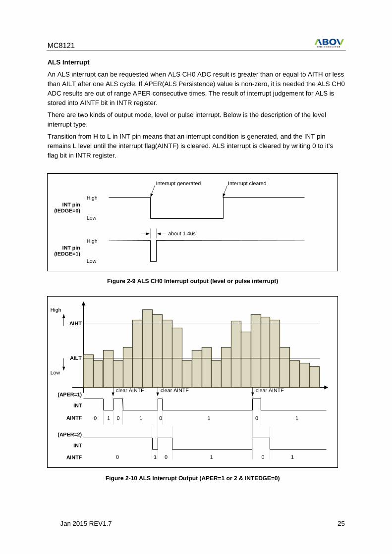
ALS Interrupt
An ALS interrupt can be requested when ALS CH0 ADC result is greater than or equal to AITH or less than AILT after one ALS cycle. If APER(ALS Persistence) value is non-zero, it is needed the ALS CH0 ADC results are out of range APER consecutive times. The result of interrupt judgement for ALS is stored into AINTF bit in INTR register.
There are two kinds of output mode, level or pulse interrupt. Below is the description of the level interrupt type.
Transition from H to L in INT pin means that an interrupt condition is generated, and the INT pin remains L level until the interrupt flag(AINTF) is cleared. ALS interrupt is cleared by writing 0 to it’s flag bit in INTR register.
INT pin (IEDGE=0)
High
Low
Interrupt generated Interrupt cleared
INT pin (IEDGE=1)
High
Low
about 1.4us
AILT
AIHT
High
Low
INT
INT
(APER=1)
(APER=2)
AINTF
AINTF 0 1 0 1 1 0
0 0 0 0 1 1 1 1
clear AINTF clear AINTF clear AINTF
Figure 2-10 ALS Interrupt Output (APER=1 or 2 & INTEDGE=0)
Figure 2-9 ALS CH0 Interrupt output (level or pulse interrupt)
MC8121
26 Jan 2015 REV1.7
2.3.4 POWER CONSUMPTION
Power consumption can be controlled through the use of the wait state timing because the wait state consumes only 60uA of power.
MC8121
Jan 2015 REV1.7 27
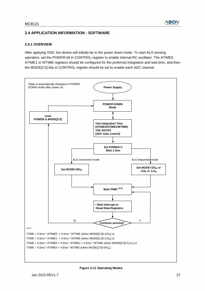
2.4 APPLICATION INFORMATION : SOFTWARE
2.4.1 OVERVIEW
After applying VDD, the device will initially be in the power down mode. To start ALS sensing operation, set the POWER bit in CONTROL register to enable internal RC oscillator. The ATIME0, ATIME1 or WTIME registers should be configured for the preferred integration and wait time, and then the MODE[2:0] bits in CONTROL register should be set to enable each ADC channel.
Power Supply
POWER DOWN Mode
•Set Integration Time (ATIME0/ATIME1/WTIME) •Set AGC0/1 (ADC Gain control)
Set POWER=1 Wait 1.4ms
State is automatically changed to POWER DOWN mode after power on.
Wait ITIME NOTE
• Wait Interrupt or •Read Data Registers
reset POWER & MODE[2:0]
Set MODE=101B or 110B or 111B Set MODE=001B
Continue sensing? N Y
ALS concurrent mode ALS sequential mode
NOTE
ITIME = 4.5ms * ATIME0 + 4.5ms * WTIME (when MODE[2:0]=101B) or ITIME = 4.5ms * ATIME1 + 4.5ms * WTIME (when MODE[2:0]=110B) or ITIME = 4.5ms * ATIME0 + 4.5ms * ATIME1 + 4.5ms * WTIME (when MODE[2:0]=111B) or ITIME = 4.5ms * ATIME0 + 4.5ms * WTIME (when MODE[2:0]=001B)
Figure 2-11 Operating Modes
MC8121
28 Jan 2015 REV1.7
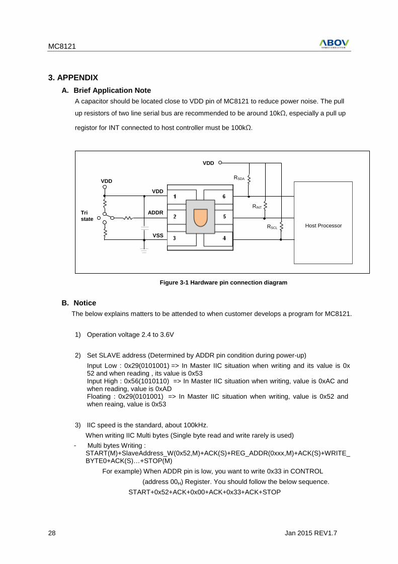
3. APPENDIX A. Brief Application Note
A capacitor should be located close to VDD pin of MC8121 to reduce power noise. The pull
up resistors of two line serial bus are recommended to be around 10kΩ, especially a pull up
registor for INT connected to host controller must be 100kΩ.
B. Notice The below explains matters to be attended to when customer develops a program for MC8121.
1) Operation voltage 2.4 to 3.6V
2) Set SLAVE address (Determined by ADDR pin condition during power-up)
Input Low : 0x29(0101001) => In Master IIC situation when writing and its value is 0x52 and when reading , its value is 0x53 Input High : 0x56(1010110) => In Master IIC situation when writing, value is 0xAC and when reading, value is 0xAD Floating : 0x29(0101001) => In Master IIC situation when writing, value is 0x52 and when reaing, value is 0x53
3) IIC speed is the standard, about 100kHz. When writing IIC Multi bytes (Single byte read and write rarely is used)
- Multi bytes Writing : START(M)+SlaveAddress_W(0x52,M)+ACK(S)+REG_ADDR(0xxx,M)+ACK(S)+WRITE_BYTE0+ACK(S)…+STOP(M)
For example) When ADDR pin is low, you want to write 0x33 in CONTROL (address 00H) Register. You should follow the below sequence.
START+0x52+ACK+0x00+ACK+0x33+ACK+STOP
Host Processor
VDD
Tri state
VDD
RSDA
RINT
RSCL
VDD
ADDR
VSS
Figure 3-1 Hardware pin connection diagram
MC8121
Jan 2015 REV1.7 29
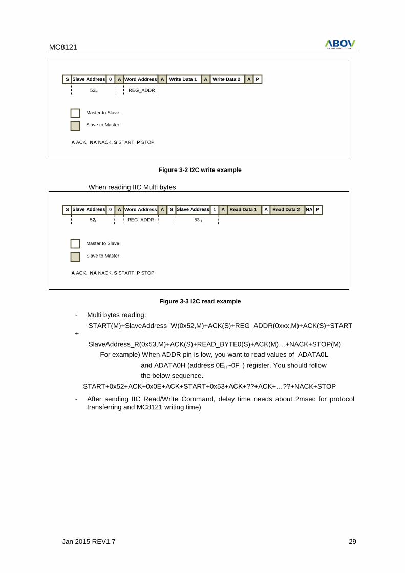
When reading IIC Multi bytes
- Multi bytes reading: START(M)+SlaveAddress_W(0x52,M)+ACK(S)+REG_ADDR(0xxx,M)+ACK(S)+START
+ SlaveAddress_R(0x53,M)+ACK(S)+READ_BYTE0(S)+ACK(M)…+NACK+STOP(M)
For example) When ADDR pin is low, you want to read values of ADATA0L and ADATA0H (address 0EH~0FH) register. You should follow the below sequence.
START+0x52+ACK+0x0E+ACK+START+0x53+ACK+??+ACK+…??+NACK+STOP
- After sending IIC Read/Write Command, delay time needs about 2msec for protocol transferring and MC8121 writing time)
Slave Address S 0 A
Word Address
A P Read Data 1
Master to Slave
Slave to Master
A ACK, NA NACK, S START, P STOP
S
Slave Address 1
A
A
Read Data 2
NA
52H 53H REG_ADDR
Slave Address S 0 A
Word Address
A A A P Write Data 1 Write Data 2
Master to Slave
Slave to Master
A ACK, NA NACK, S START, P STOP
52H REG_ADDR
Figure 3-2 I2C write example
Figure 3-3 I2C read example