Embed Size (px)
Citation preview

MCP19035High-Speed Synchronous Buck Controller
Features:
• Input Voltage Range: from 4.5V to 30V
• Targeted for Low-Voltage Power Trains with Output Current up to 20A
• High-Speed Voltage Mode, Analog Pulse-Width Modulation Control
• Power Good Output
• Internal Oscillator, Reference Voltage and Overcurrent Limit Threshold for Stand-Alone Applications.
• Multiple Switching Frequency Options (FSW):
- 300 kHz
- 600 kHz
• Integrated Synchronous MOSFET Drivers
• Multiple Dead-Time Options
• Internal Blocking Device for Bootstrap Circuit
• Integrated Current Sense Capability for Short Circuit Protection
• Internal Overtemperature Protection
• Under Voltage Lockout (UVLO)
• Integrated Linear Voltage Regulator
• 10-LD 3 X 3 mm DFN Package
Applications:
• Point of Loads
• Set-Top Boxes
• DSL Cable Modems
• FPGA’s/DSP’s Power Supply
• PC’s Graphic/Audio Cards
General Description
The MCP19035 is an application-optimized, high-speed synchronous buck controller that operates frominput voltage sources up to 30V. This controllerimplements a voltage-mode control architecture with afixed switching frequency of 300 kHz or 600 kHz. Thehigh-switching frequency facilitates the use of smallerpassive components, including the inductor andinput/output capacitors, allowing a compact, high-performance power supply solution. The MCP19035implements an adaptive anti-cross conduction schemeto prevent shoot-through in the external powerMOSFETs. Furthermore, the MCP19035 offers multipledead-time options, enabling an additional degree ofoptimization, allowing a higher efficiency power supplydesign.
The MCP19035 controller is intended to be used forapplications providing up to 20A of output currentsacross a wide input voltage range, up to 30V.
The SHDN input is used to turn the device on and off.While turned off, the current consumption is minimized.
The MCP19035 offers a Power Good feature(PWRGD), enabling fault detection and simplifyingsequencing.
Package Types
MCP190353x3 DFN*
COMP
FB
VIN
PHASE
BOOT
1
2
3
4
10
9
8
7 LDRV
HDRVSHDN
* Includes Exposed Thermal Pad (EP); see Table 3-1.
EP11
6PWRGD +VCC5
2012-2013 Microchip Technology Inc. DS22326B-page 1
MCP19035
Typical Application
CIN
COUT
L
Q1
Q2
MCP19035
HDRV
LDRV
PHASE
BOOT
+VCC
CBOOT
CVCC
+VOUT
VIN
PWRGD
COMP
FB
R1
R3C1R2
C3R4
C2
ON
OFF SHDN
GND
+VIN
DS22326B-page 2 2012-2013 Microchip Technology Inc.
MCP19035
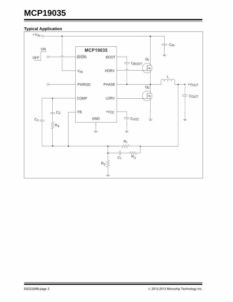
1.0 ELECTRICAL CHARACTERISTICS
Absolute Maximum Ratings †
VIN - VGND........................................................ -0.3V to +32V
VBOOT................................................................ -0.3V to +37V
VHDRV, HDRV Pin................. +VPHASE -0.3V to VBOOT+0.3V
VLDRV, LDRV Pin.....................+ (VGND-0.3V) to (VCC+0.3V)
Max. Voltage on Any Pin ...........+ (VGND-0.3V) to (VCC+0.3V)
Storage Temperature ....................................-65°C to +150°C
Maximum Junction Temperature................................. +150°C
ESD protection on all pins (HBM) .................................... 2 kV
ESD protection on all pins (MM) .....................................200V
† Notice: Stresses above those listed under “MaximumRatings” may cause permanent damage to the device.This is a stress rating only and functional operation ofthe device at those or any other conditions above thoseindicated in the operational sections of thisspecification is not intended. Exposure to maximumrating conditions for extended periods may affectdevice reliability.
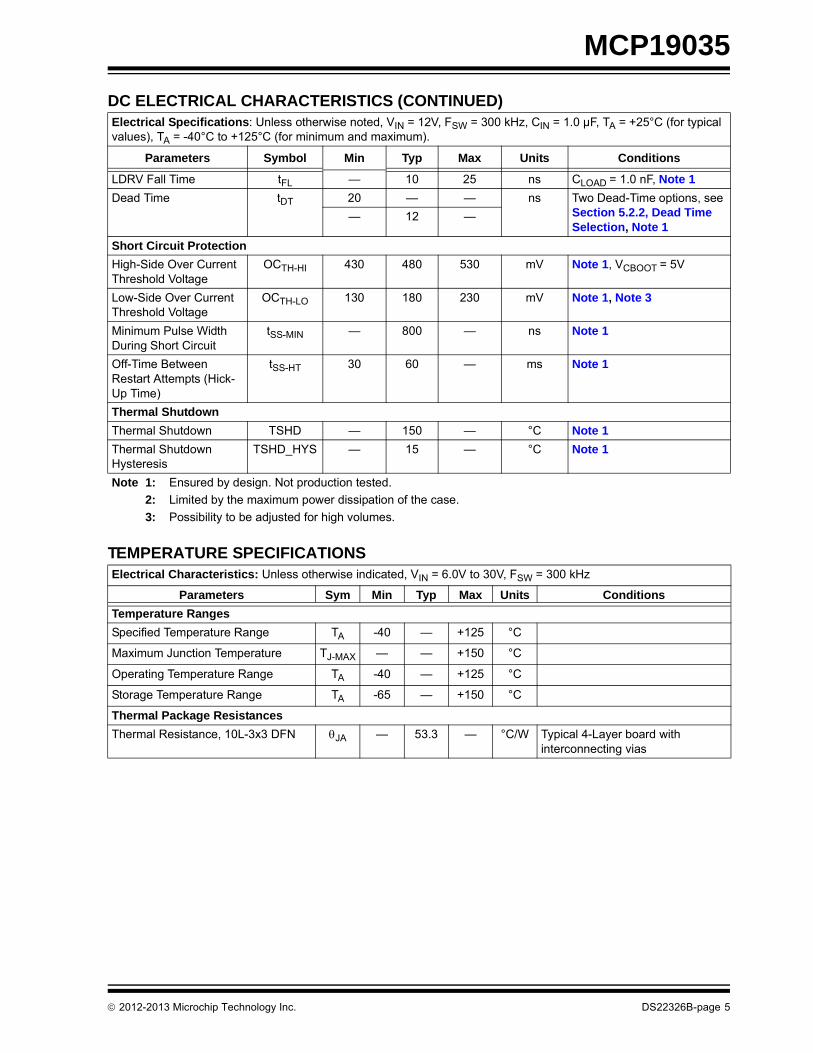
DC ELECTRICAL CHARACTERISTICSElectrical Specifications: Unless otherwise noted, VIN = 12V, FSW = 300 kHz, CIN = 1.0 µF, TA = +25°C (for typical values), TA = -40°C to +125°C (for minimum and maximum).
Parameters Symbol Min Typ Max Units Conditions
Inputs
Input Voltage Range VIN 4.5 — 30 V
UVLO (VIN Rising) UVLOON 4 4.2 4.4 V
UVLO (VIN Falling) UVLOOFF 3.4 3.6 3.8 V
UVLO Hysteresis UVLOHYST — 600 — mV
Input Quiescent Current I(VIN) — 6 8 mA
Shutdown Current IIN_SHDN — 25 50 µA SHDN = GND. Internal Voltage Regulator is also disabled
Linear Regulator
Output Voltage VCC 4.875 5 5.125 V 6V VIN < 30V
Output Current IVCC-OUT 50 — mA 6.5V VIN < 30V, Note 2
Short-Circuit Output Current
IVCC-OUT_SC — — 100 mA VIN = 6V, RLOAD < 0.1
Load Regulation — 0.1 — % Note 1
Line Regulation — 0.05 — % Note 1
Dropout Voltage — 0.75 1.3 V IVCC_OUT = 50 mA
Power Supply Rejection Ratio
PSRR — 70 — dB f 1000 Hz,IVCC_OUT = 50 mACIN = 0 µF, CVCC-OUT = 4.7 µF, Note 1
Internal Oscillator
Switching Frequency FSW 255 300 345 kHz 2 options, see Section 4.4, Internal Oscillator510 600 690 kHz
Ramp Signal Amplitude VRAMP 0.9 1 1.1 VPP Note 1
Reference Voltage
Reference Voltage Generator
VREF 585 600 615 mV
Note 1: Ensured by design. Not production tested.
2: Limited by the maximum power dissipation of the case.
3: Possibility to be adjusted for high volumes.
2012-2013 Microchip Technology Inc. DS22326B-page 3
MCP19035
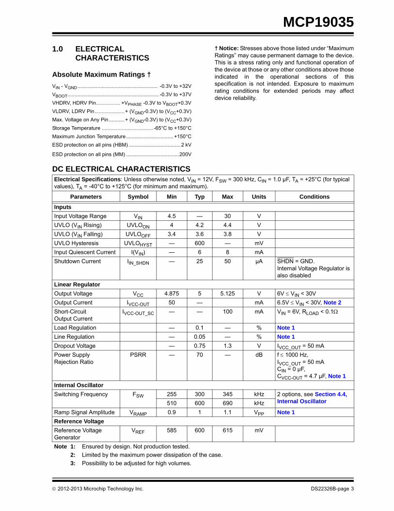
Error Amplifier
Gain Bandwidth Product GBP 6.5 10 — MHz Note 1
Open Loop Gain AOL 70 80 — dB Note 1
Input Offset Voltage VOS -5 0.1 5 mV Note 1
Input Bias Current (FB Pin)
IBIAS — — 5 nA Note 1
Error Amplifier Sink Current
ISINK — 5 — mA Note 1
Error Amplifier Source Current
ISOURCE — 5 — mA Note 1
PWM Section
Maximum Duty Cycle DCMAX 85 — — % Note 1
Minimum ON time tON(MIN) 50 — 100 ns 6V VIN < 30V, Note 1
Soft Start
Soft Start Time tSS — 8 — ms
Shutdown
Logic Low-to-High Threshold
SHDNHI 0.85 — — V 4.5V VIN < 30V, VCC goes from 0V to 5V
Logic High-to-Low Threshold
SHDNLO — — 0.4 V 4.5V VIN < 30V, VCC goes from 5V to 0V
Power Good
Power Good Threshold High
PGTH-H — 93 96 % of VREF
Power Good Threshold Low
PGTH-LOW 88 90 — % of VREF
Power Good Threshold Hysteresis
PGTH-HYS — 3 — % of VREF
Power Good Delay tPG-DELAY — 150 — us VFB = (PGTH-HI + 100 mV) to (PGTH-LOW – 100 mV)
Power Good Active Time-Out Period
tPG-TIME-OUT — 120 — ms VFB = (PGTH-HI – 100 mV) to (PGTH-HI + 100 mV)
MOSFET Drivers
High-Side Driver Pull-up Resistance
RHI-SOURCE — 2 3.5 VBOOT – VPHASE = 4.5V, IHDRV = 100 mA, Note 1
High-Side Driver Pull-Down Resistance
RHI-SINK — 2 3.5 VBOOT – VPHASE = 4.5V, IHDRV = 100 mA, Note 1
Low-Side Driver Pull-Up Resistance
RLO-SOURCE — 2 3.5 VCC = 5V, Note 1
Low-Side Driver Pull-Down Resistance
RLO-SINK — 1 2.5 VCC = 5V, Note 1
HDRV Rise Time tRH — 15 35 ns CLOAD = 1.0 nF, Note 1
HDRV Fall Time tFH — 15 35 ns CLOAD = 1.0 nF, Note 1
LDRV Rise Time tRL — 10 25 ns CLOAD = 1.0 nF, Note 1
DC ELECTRICAL CHARACTERISTICS (CONTINUED)Electrical Specifications: Unless otherwise noted, VIN = 12V, FSW = 300 kHz, CIN = 1.0 µF, TA = +25°C (for typical values), TA = -40°C to +125°C (for minimum and maximum).
Parameters Symbol Min Typ Max Units Conditions
Note 1: Ensured by design. Not production tested.
2: Limited by the maximum power dissipation of the case.
3: Possibility to be adjusted for high volumes.
DS22326B-page 4 2012-2013 Microchip Technology Inc.
MCP19035
LDRV Fall Time tFL — 10 25 ns CLOAD = 1.0 nF, Note 1
Dead Time tDT 20 — — ns Two Dead-Time options, see Section 5.2.2, Dead Time Selection, Note 1
— 12 —
Short Circuit Protection
High-Side Over Current Threshold Voltage
OCTH-HI 430 480 530 mV Note 1, VCBOOT = 5V
Low-Side Over Current Threshold Voltage
OCTH-LO 130 180 230 mV Note 1, Note 3
Minimum Pulse Width During Short Circuit
tSS-MIN — 800 — ns Note 1
Off-Time Between Restart Attempts (Hick-Up Time)
tSS-HT 30 60 — ms Note 1
Thermal Shutdown
Thermal Shutdown TSHD — 150 — °C Note 1
Thermal Shutdown Hysteresis
TSHD_HYS — 15 — °C Note 1
TEMPERATURE SPECIFICATIONSElectrical Characteristics: Unless otherwise indicated, VIN = 6.0V to 30V, FSW = 300 kHz
Parameters Sym Min Typ Max Units Conditions
Temperature Ranges
Specified Temperature Range TA -40 — +125 °C
Maximum Junction Temperature TJ-MAX — — +150 °C
Operating Temperature Range TA -40 — +125 °C
Storage Temperature Range TA -65 — +150 °C
Thermal Package Resistances
Thermal Resistance, 10L-3x3 DFN JA — 53.3 — °C/W Typical 4-Layer board with interconnecting vias
DC ELECTRICAL CHARACTERISTICS (CONTINUED)Electrical Specifications: Unless otherwise noted, VIN = 12V, FSW = 300 kHz, CIN = 1.0 µF, TA = +25°C (for typical values), TA = -40°C to +125°C (for minimum and maximum).
Parameters Symbol Min Typ Max Units Conditions
Note 1: Ensured by design. Not production tested.
2: Limited by the maximum power dissipation of the case.
3: Possibility to be adjusted for high volumes.
2012-2013 Microchip Technology Inc. DS22326B-page 5

MCP19035
NOTES:
DS22326B-page 6 2012-2013 Microchip Technology Inc.
MCP19035
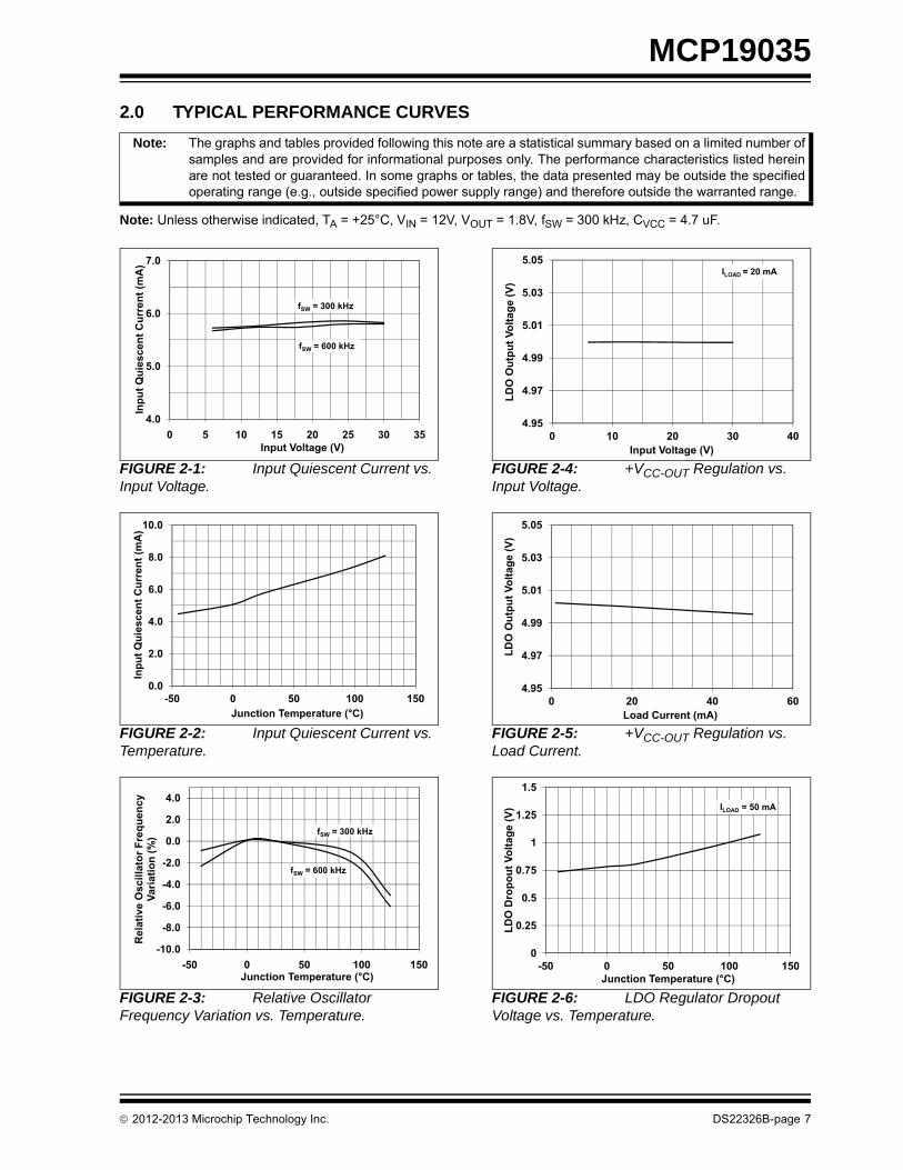
2.0 TYPICAL PERFORMANCE CURVES
Note: Unless otherwise indicated, TA = +25°C, VIN = 12V, VOUT = 1.8V, fSW = 300 kHz, CVCC = 4.7 uF.
FIGURE 2-1: Input Quiescent Current vs. Input Voltage.
FIGURE 2-2: Input Quiescent Current vs. Temperature.
FIGURE 2-3: Relative Oscillator Frequency Variation vs. Temperature.
FIGURE 2-4: +VCC-OUT Regulation vs. Input Voltage.
FIGURE 2-5: +VCC-OUT Regulation vs. Load Current.
FIGURE 2-6: LDO Regulator Dropout Voltage vs. Temperature.
Note: The graphs and tables provided following this note are a statistical summary based on a limited number ofsamples and are provided for informational purposes only. The performance characteristics listed hereinare not tested or guaranteed. In some graphs or tables, the data presented may be outside the specifiedoperating range (e.g., outside specified power supply range) and therefore outside the warranted range.
5.0
6.0
7.0
iesc
ent C
urre
nt (m
A)
fSW = 300 kHz
fSW = 600 kHz
4.00 5 10 15 20 25 30 35
Inpu
t Qu
Input Voltage (V)
4.0
6.0
8.0
10.0
iesc
ent C
urre
nt (m
A)
0.0
2.0
-50 0 50 100 150
Inpu
t Qui
Junction Temperature (°C)
-4.0
-2.0
0.0
2.0
4.0
Osc
illat
or F
requ
ency
Va
riatio
n (%
) fSW = 300 kHz
fSW = 600 kHz
-10.0
-8.0
-6.0
-50 0 50 100 150
Rel
ativ
eO V
Junction Temperature (°C)
4.99
5.01
5.03
5.05
Out
put V
olta
ge (V
)
ILOAD = 20 mA
4.95
4.97
0 10 20 30 40
LDO
O
Input Voltage (V)
4.99
5.01
5.03
5.05 O
utpu
t Vol
tage
(V)
4.95
4.97
0 20 40 60
LDO
Load Current (mA)
0 5
0.75
1
1.25
1.5
ropo
ut V
olta
ge (V
) ILOAD = 50 mA
0
0.25
0.5
-50 0 50 100 150
LDO
Dr
Junction Temperature (°C)
2012-2013 Microchip Technology Inc. DS22326B-page 7
MCP19035
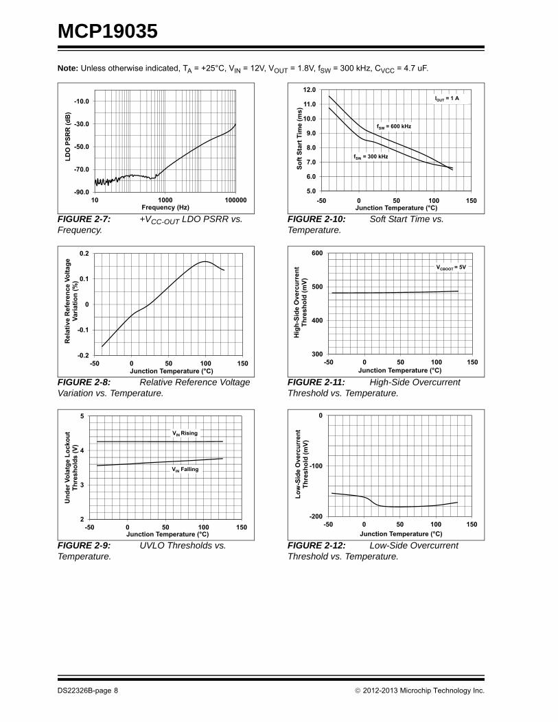
Note: Unless otherwise indicated, TA = +25°C, VIN = 12V, VOUT = 1.8V, fSW = 300 kHz, CVCC = 4.7 uF.
FIGURE 2-7: +VCC-OUT LDO PSRR vs. Frequency.
FIGURE 2-8: Relative Reference Voltage Variation vs. Temperature.
FIGURE 2-9: UVLO Thresholds vs. Temperature.
FIGURE 2-10: Soft Start Time vs. Temperature.
FIGURE 2-11: High-Side Overcurrent Threshold vs. Temperature.
FIGURE 2-12: Low-Side Overcurrent Threshold vs. Temperature.
-50.0
-30.0
-10.0
LDO
PSR
R (d
B)
-90.0
-70.0
10 1000 100000
L
Frequency (Hz)
0
0.1
0.2
ve R
efer
ence
Vol
tage
Va
riatio
n (%
)
-0.2
-0.1
-50 0 50 100 150
Rel
ativ
Junction Temperature (°C)
3
4
5
Vola
tge
Lock
out
hres
hold
s (V
)
VIN Rising
VIN Falling
2
3
-50 0 50 100 150
Und
er Th
Junction Temperature (°C)
8.0
9.0
10.0
11.0
12.0
t Sta
rt T
ime
(ms)
IOUT = 1 A
fSW = 600 kHz
fSW = 300 kHz
5.0
6.0
7.0
-50 0 50 100 150
Soft
Junction Temperature (°C)
fSW 300 kHz
400
500
600
Side
Ove
rcur
rent
hr
esho
ld (m
V)
VCBOOT = 5V
300
400
-50 0 50 100 150
Hig
h- Th
Junction Temperature (°C)
-100
0
-Sid
e O
verc
urre
nt
hres
hold
(mV)
-200-50 0 50 100 150
Low
- T
Junction Temperature (°C)
DS22326B-page 8 2012-2013 Microchip Technology Inc.
MCP19035
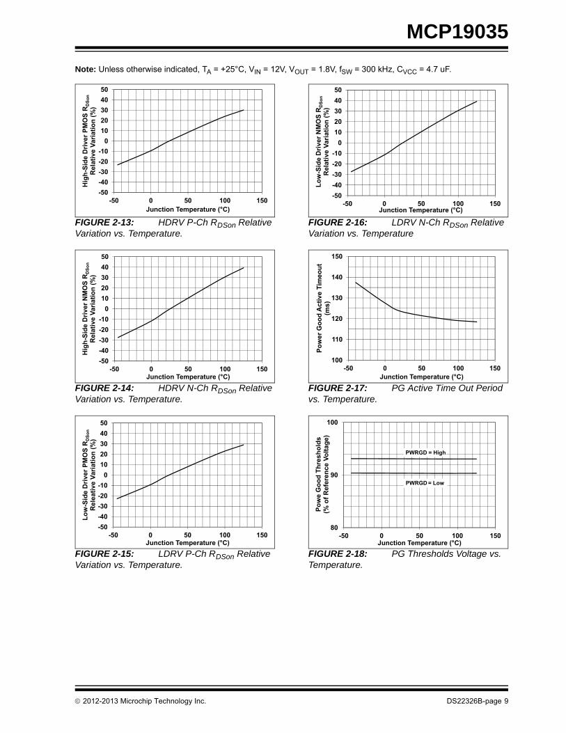
Note: Unless otherwise indicated, TA = +25°C, VIN = 12V, VOUT = 1.8V, fSW = 300 kHz, CVCC = 4.7 uF.
FIGURE 2-13: HDRV P-Ch RDSon Relative Variation vs. Temperature.
FIGURE 2-14: HDRV N-Ch RDSon Relative Variation vs. Temperature.
FIGURE 2-15: LDRV P-Ch RDSon Relative Variation vs. Temperature.
FIGURE 2-16: LDRV N-Ch RDSon Relative Variation vs. Temperature
FIGURE 2-17: PG Active Time Out Period vs. Temperature.
FIGURE 2-18: PG Thresholds Voltage vs. Temperature.
20-10
01020304050
de D
river
PM
OS
RD
Son
tive
Varia
tion
(%)
-50-40-30-20
-50 0 50 100 150
Hig
h-Si
dR
elat
Junction Temperature (°C)
-100
1020304050
e D
river
NM
OS
RD
Son
tive
Varia
tion
(%)
-50-40-30-20
-50 0 50 100 150
Hig
h-Si
deR
elat
Junction Temperature (°C)
-100
1020304050
e D
river
PM
OS
RD
Son
tive
Varia
tion
(%)
-50-40-30-20
-50 0 50 100 150
Low
-Sid
eR
elea
t
Junction Temperature (°C)
-100
1020304050
e D
river
NM
OS
RD
Son
tive
Varia
tion
(%)
-50-40-30-20
-50 0 50 100 150
Low
-Sid
eR
elat
Junction Temperature (°C)
120
130
140
150
Goo
d A
ctiv
e Ti
meo
ut
(ms)
100
110
-50 0 50 100 150
Pow
er G
Junction Temperature (°C)
90
100
Goo
d Th
resh
olds
R
efer
ence
Vol
tage
)
PWRGD = Low
PWRGD = High
80-50 0 50 100 150
Pow
e (%
of R
Junction Temperature (°C)
2012-2013 Microchip Technology Inc. DS22326B-page 9

MCP19035
NOTES:
DS22326B-page 10 2012-2013 Microchip Technology Inc.
MCP19035
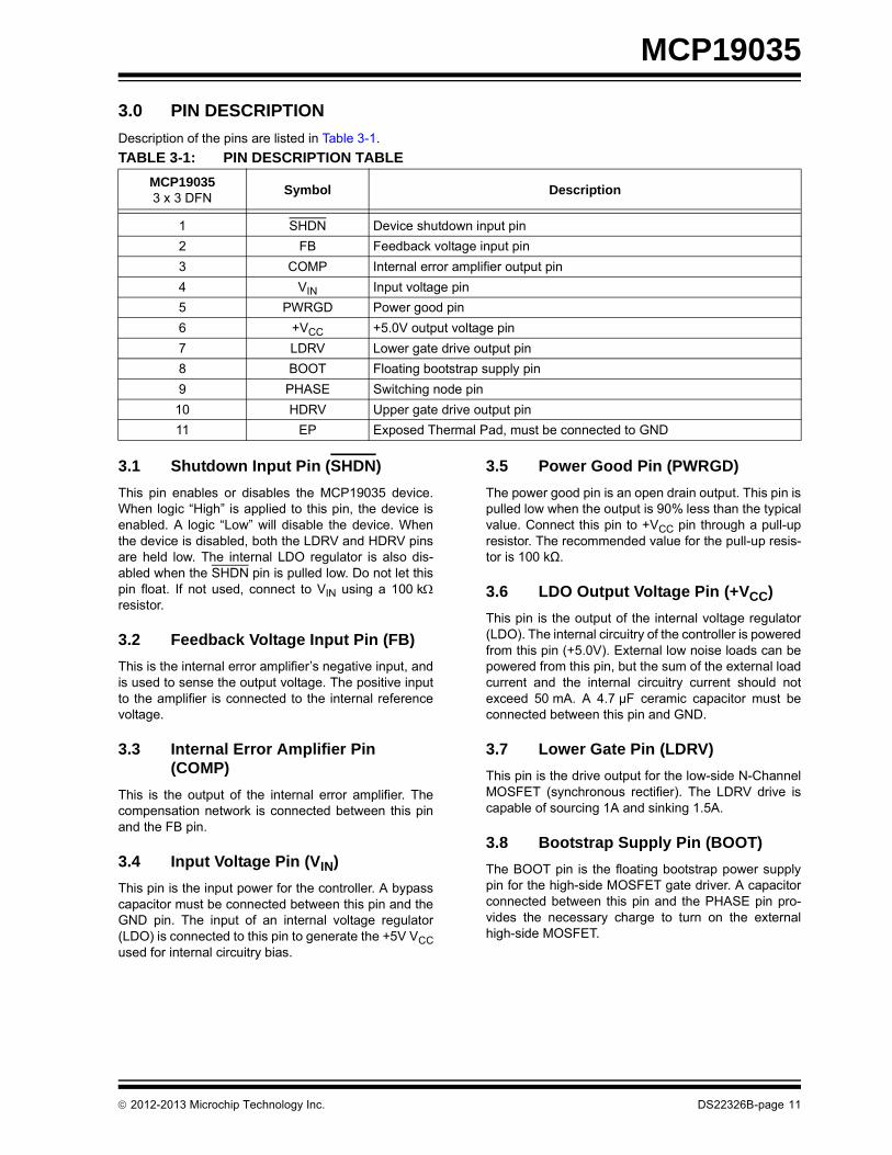
3.0 PIN DESCRIPTION
Description of the pins are listed in Table 3-1.
3.1 Shutdown Input Pin (SHDN)
This pin enables or disables the MCP19035 device.When logic “High” is applied to this pin, the device isenabled. A logic “Low” will disable the device. Whenthe device is disabled, both the LDRV and HDRV pinsare held low. The internal LDO regulator is also dis-abled when the SHDN pin is pulled low. Do not let thispin float. If not used, connect to VIN using a 100 kresistor.
3.2 Feedback Voltage Input Pin (FB)
This is the internal error amplifier’s negative input, andis used to sense the output voltage. The positive inputto the amplifier is connected to the internal referencevoltage.
3.3 Internal Error Amplifier Pin (COMP)
This is the output of the internal error amplifier. Thecompensation network is connected between this pinand the FB pin.
3.4 Input Voltage Pin (VIN)
This pin is the input power for the controller. A bypasscapacitor must be connected between this pin and theGND pin. The input of an internal voltage regulator(LDO) is connected to this pin to generate the +5V VCCused for internal circuitry bias.
3.5 Power Good Pin (PWRGD)
The power good pin is an open drain output. This pin ispulled low when the output is 90% less than the typicalvalue. Connect this pin to +VCC pin through a pull-upresistor. The recommended value for the pull-up resis-tor is 100 kΩ.
3.6 LDO Output Voltage Pin (+VCC)
This pin is the output of the internal voltage regulator(LDO). The internal circuitry of the controller is poweredfrom this pin (+5.0V). External low noise loads can bepowered from this pin, but the sum of the external loadcurrent and the internal circuitry current should notexceed 50 mA. A 4.7 μF ceramic capacitor must beconnected between this pin and GND.
3.7 Lower Gate Pin (LDRV)
This pin is the drive output for the low-side N-ChannelMOSFET (synchronous rectifier). The LDRV drive iscapable of sourcing 1A and sinking 1.5A.
3.8 Bootstrap Supply Pin (BOOT)
The BOOT pin is the floating bootstrap power supplypin for the high-side MOSFET gate driver. A capacitorconnected between this pin and the PHASE pin pro-vides the necessary charge to turn on the externalhigh-side MOSFET.
TABLE 3-1: PIN DESCRIPTION TABLE
MCP190353 x 3 DFN
Symbol Description
1 SHDN Device shutdown input pin
2 FB Feedback voltage input pin
3 COMP Internal error amplifier output pin
4 VIN Input voltage pin
5 PWRGD Power good pin
6 +VCC +5.0V output voltage pin
7 LDRV Lower gate drive output pin
8 BOOT Floating bootstrap supply pin
9 PHASE Switching node pin
10 HDRV Upper gate drive output pin
11 EP Exposed Thermal Pad, must be connected to GND
2012-2013 Microchip Technology Inc. DS22326B-page 11

MCP19035
3.9 Switching Node Pin (PHASE)
This pin provides a return path for the high-side gatedriver. It also provides a path for the charging of theBOOT capacitor, used while turning on the high-sideMOSFET. This pin also senses the switching transitionto eliminate cross conduction (shoot-through).
3.10 Upper Gate Drive Pin (HDRV)
This pin is the high-side N-channel MOSFET (controltransistor) gate drive output. The HDRV drive iscapable of sourcing and sinking 1A.
3.11 Exposed Thermal Pad (EP)
Analog ground and power ground are both connectedto this pin.
DS22326B-page 12 2012-2013 Microchip Technology Inc.
MCP19035
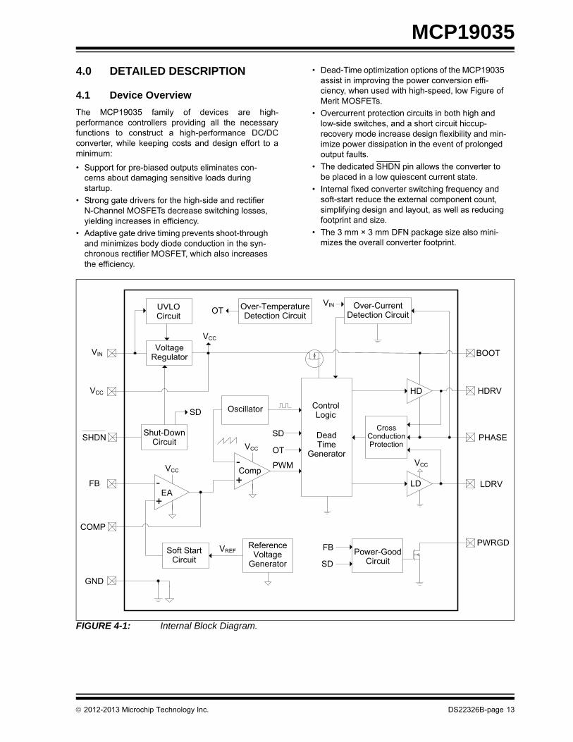
4.0 DETAILED DESCRIPTION
4.1 Device Overview
The MCP19035 family of devices are high-performance controllers providing all the necessaryfunctions to construct a high-performance DC/DCconverter, while keeping costs and design effort to aminimum:
• Support for pre-biased outputs eliminates con-cerns about damaging sensitive loads during startup.
• Strong gate drivers for the high-side and rectifier N-Channel MOSFETs decrease switching losses, yielding increases in efficiency.
• Adaptive gate drive timing prevents shoot-through and minimizes body diode conduction in the syn-chronous rectifier MOSFET, which also increases the efficiency.
• Dead-Time optimization options of the MCP19035 assist in improving the power conversion effi-ciency, when used with high-speed, low Figure of Merit MOSFETs.
• Overcurrent protection circuits in both high and low-side switches, and a short circuit hiccup-recovery mode increase design flexibility and min-imize power dissipation in the event of prolonged output faults.
• The dedicated SHDN pin allows the converter to be placed in a low quiescent current state.
• Internal fixed converter switching frequency and soft-start reduce the external component count, simplifying design and layout, as well as reducing footprint and size.
• The 3 mm × 3 mm DFN package size also mini-mizes the overall converter footprint.
FIGURE 4-1: Internal Block Diagram.
HDRV
LDRV
Oscillator
BOOT
ControlLogic
SHDN
VIN
PWRGD
COMP
FB
PHASECross
ConductionProtection
HD
LD
VoltageRegulator
Comp
DeadTime
Generator
+
-
VCC
Power-GoodCircuit
Shut-DownCircuit
+
-
SD
EA
SD
UVLOCircuit
Over-CurrentDetection Circuit
ReferenceVoltage
GeneratorSoft Start
CircuitFB
SD
GND
VREF
PWM
Over-TemperatureDetection CircuitOT
OT
VIN
VCC
VCC
VCC
VCC
2012-2013 Microchip Technology Inc. DS22326B-page 13
MCP19035
4.2 PWM Circuitry
The MCP19035 controller implements a fixedfrequency, voltage-mode control scheme. The internalPWM generator is comprised of an oscillator, erroramplifier, high-speed comparator and a latch. The erroramplifier generates the control voltage by amplifyingthe difference between voltage reference (600 mV,internally generated) and the voltage of the FB pin(feedback voltage). This control voltage is compared bythe high-speed comparator to an artificially generatedramp signal; the result is a PWM signal. An SR latch(Set-Reset flip-flop) is used to prevent the PWMcircuitry from turning on the external switch until thebeginning of the next clock cycle.
An external Compensation Network (Type-II orType-III) must be used to stabilize the control system.
4.3 Internal Reference Voltage VREF
An integrated, precision voltage reference is providedby the MCP19035. An external resistor divider is usedto program the converter’s output voltage. The nominalvalue of this internal reference voltage is 600 mV.
4.4 Internal Oscillator
The MCP19035 device provides two switchingfrequency options: 300 kHz and 600 kHz.
4.5 Under Voltage Lockout Circuit (UVLO)
An integrated Under Voltage Lockout Circuit (UVLO)prevents the converter from starting until the input volt-age is high enough for normal operation. The converterwill typically start at 4.2V and operate down to 3.6V.Hysteresis is added to prevent starting and stoppingduring startup, as a result of loading the input voltagesource.
4.6 Shutdown Input
The Shutdown input pin (SHDN) is used to enable anddisable the controller. When the SHDN pin is pulledlow, the MCP19035 is placed in Shutdown mode.During Shutdown, most of the internal circuits(including the LDO) are disabled, to minimize currentconsumption.
A 100 kΩ pull-up resistor is recommended between theSHDN pin and VIN pin. Note that the SHDN input is ahigh-impedance pin. Noise generated by the circuitslocated near this pin may inadvertently shut down thecontroller. To improve the noise immunity of this inputpin, we recommend placing a small capacitor betweenGND and SHDN, or decrease the value of the pull-upresistor. The Shutdown input pin should not be leftfloating.
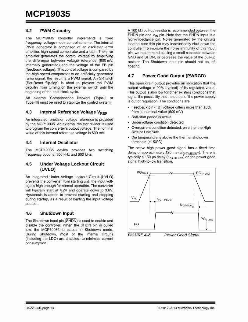
4.7 Power Good Output (PWRGD)
This open drain output provides an indication that theoutput voltage is 92% (typical) of its regulated value.This output is also low for other existing conditions thatsignal the possibility that the output of the power supplyis out of regulation. The conditions are:
• Feedback pin (FB) voltage differs more than ±8% from its nominal value (600 mV)
• Soft-start period is active
• Undervoltage condition detected
• Overcurrent condition detected, on either the High Side or Low Side
• Die temperature is above the thermal shutdown threshold (+150°C)
The active high power good signal has a fixed timedelay of approximately 120 ms (tPG-TIMEOUT). There istypically a 150 μs delay (tPG-DELAY) on the power goodsignal high-to-low transition.
FIGURE 4-2: Power Good Signal.
PGTH-LOW
tPG-TIMEOUT
PG
VFB
tPG-DELAY
PGTH-HI
PGV-LOW
DS22326B-page 14 2012-2013 Microchip Technology Inc.

MCP19035
4.8 Internal Voltage Regulator (LDO)
The MCP19035 controller offers an internal 5V LowDropout Voltage Regulator. This regulator provides thebias voltage for all internal circuits. A ceramic capacitor(4.7 μF minimum) must be connected between theoutput of this LDO (VCC pin) and ground (GND pin) forstable operation.
An external low noise load may be powered from thisregulator, but the total current consumed from the LDOoutput (internal circuitry of MCP19035 + external load)should not exceed 50 mA. The internal circuitry of theMCP19035 consume approximately 5 mA. The totalamount of current available to power the external loadcan be estimated from Equation 4-1:
EQUATION 4-1:
This LDO dissipates power within the MCP19035. Toavoid tripping the Overtemperature Protection Circuit,the designer must ensure that the maximum dietemperature is below +125°C under worst caseconditions (i.e. high input voltage). For furtherinformation regarding the maximum dissipated powerfor LDOs, see Microchip’s AN761 and AN792application notes.
The LDO is protected against overload and short-circuitconditions. Consistent performance of the internalMOS drivers is ensured by monitoring the LDO outputvoltage; if the voltage is lower than 3.3V typical, thechip will enter in Shut-Down mode to prevent damageto the external MOSFETs.
4.9 Internal MOSFET Drivers
Internal MOSFET drivers are capable of drivingexternal, “Logic Level” (+5V) MOSFETs.
The Low-Side Driver (LDRV) is referenced to the GNDpin and is capable of sourcing 1A and sinking 1.5A.
The High-Side Driver (HDRV) is floating and capable ofsourcing and sinking 1A. This driver is powered from anexternal bootstrap capacitor.
The drivers have non-overlapping timing that isgoverned by an adaptive delay circuit to minimize bodydiode conduction in the synchronous rectifier.
For the optimized Dead Time version of theMCP19035, the adaptive delay circuit is disabled andthe Dead Time has a fixed value.
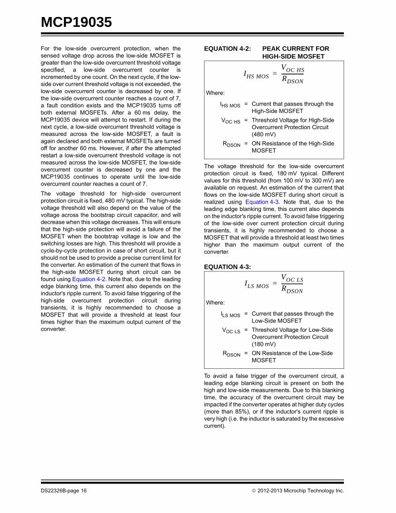
4.10 Overcurrent Protection
Overcurrent protection is accomplished by monitoringthe voltage across the external MOSFETs when theyare ON (conducting).
For the high-side overcurrent protection, when thesensed voltage drop across the high-side MOSFET isgreater than the high-side overcurrent thresholdvoltage, the high-side MOSFET is immediately turnedoff and the high-side overcurrent counter isincremented by one. On the next cycle, if the high-sideovercurrent threshold voltage is not exceeded, thehigh-side overcurrent counter is decreased by onecount. If the high-side overcurrent counter reaches acount of 7, a fault condition exists and the MCP19035turns off both external MOSFETs.
After a 60 ms delay, the MCP19035 will attempt torestart. If during the next cycle, a high-side overcurrentthreshold voltage is measured across the high-sideMOSFET, a fault is again declared and both externalMOSFETs are turned off for another 60 ms. However, ifafter the attempted restart a high-side overcurrentthreshold voltage is not measured across the high-sideMOSFET, the high-side overcurrent counter isdecreased by one and the MCP19035 continues tooperate until the high-side overcurrent counter reachesa count of 7.
The low-side overcurrent protection behaves much thesame way as the high-side overcurrent protection. Thedifference is that the low-side MOSFET is notimmediately turned off when a low-side overcurrentthreshold voltage is measured. It remains on until thenext cycle begins.
IExternal Load = 50 mA - fSW x (QG(High Side) + QG(Low Side)) - 5 mA
Where:
IExternal Load = Current Available for powering the External Load
fSW = Switching Frequency (300 kHz or 600 kHz)
QG(High Side) = Total Gate Charge of the High-Side MOSFET at 4.5V VGS
QG(Low Side) = Total Gate Charge of the Low-Side MOSFET at 4.5V VGS
2012-2013 Microchip Technology Inc. DS22326B-page 15
MCP19035
For the low-side overcurrent protection, when thesensed voltage drop across the low-side MOSFET isgreater than the low-side overcurrent threshold voltagespecified, a low-side overcurrent counter isincremented by one count. On the next cycle, if the low-side over current threshold voltage is not exceeded, thelow-side overcurrent counter is decreased by one. Ifthe low-side overcurrent counter reaches a count of 7,a fault condition exists and the MCP19035 turns offboth external MOSFETs. After a 60 ms delay, theMCP19035 device will attempt to restart. If during thenext cycle, a low-side overcurrent threshold voltage ismeasured across the low-side MOSFET, a fault isagain declared and both external MOSFETs are turnedoff for another 60 ms. However, if after the attemptedrestart a low-side overcurrent threshold voltage is notmeasured across the low-side MOSFET, the low-sideovercurrent counter is decreased by one and theMCP19035 continues to operate until the low-sideovercurrent counter reaches a count of 7.
The voltage threshold for high-side overcurrentprotection circuit is fixed, 480 mV typical. The high-sidevoltage threshold will also depend on the value of thevoltage across the bootstrap circuit capacitor, and willdecrease when this voltage decreases. This will ensurethat the high-side protection will avoid a failure of theMOSFET when the bootstrap voltage is low and theswitching losses are high. This threshold will provide acycle-by-cycle protection in case of short circuit, but itshould not be used to provide a precise current limit forthe converter. An estimation of the current that flows inthe high-side MOSFET during short circuit can befound using Equation 4-2. Note that, due to the leadingedge blanking time, this current also depends on theinductor's ripple current. To avoid false triggering of thehigh-side overcurrent protection circuit duringtransients, it is highly recommended to choose aMOSFET that will provide a threshold at least fourtimes higher than the maximum output current of theconverter.
EQUATION 4-2: PEAK CURRENT FOR HIGH-SIDE MOSFET
The voltage threshold for the low-side overcurrentprotection circuit is fixed, 180 mV typical. Differentvalues for this threshold (from 100 mV to 300 mV) areavailable on request. An estimation of the current thatflows on the low-side MOSFET during short circuit isrealized using Equation 4-3. Note that, due to theleading edge blanking time, this current also dependson the inductor's ripple current. To avoid false triggeringof the low-side over current protection circuit duringtransients, it is highly recommended to choose aMOSFET that will provide a threshold at least two timeshigher than the maximum output current of theconverter.
EQUATION 4-3:
To avoid a false trigger of the overcurrent circuit, aleading edge blanking circuit is present on both thehigh and low-side measurements. Due to this blankingtime, the accuracy of the overcurrent circuit may beimpacted if the converter operates at higher duty cycles(more than 85%), or if the inductor's current ripple isvery high (i.e. the inductor is saturated by the excessivecurrent).
IHS MOS
VOC HS
RDSON-----------------=
Where:
IHS MOS = Current that passes through the High-Side MOSFET
VOC HS = Threshold Voltage for High-Side Overcurrent Protection Circuit (480 mV)
RDSON = ON Resistance of the High-Side MOSFET
ILS MOS
VOC LS
RDSON-----------------=
Where:
ILS MOS = Current that passes through the Low-Side MOSFET
VOC LS = Threshold Voltage for Low-Side Overcurrent Protection Circuit (180 mV)
RDSON = ON Resistance of the Low-Side MOSFET
DS22326B-page 16 2012-2013 Microchip Technology Inc.
MCP19035
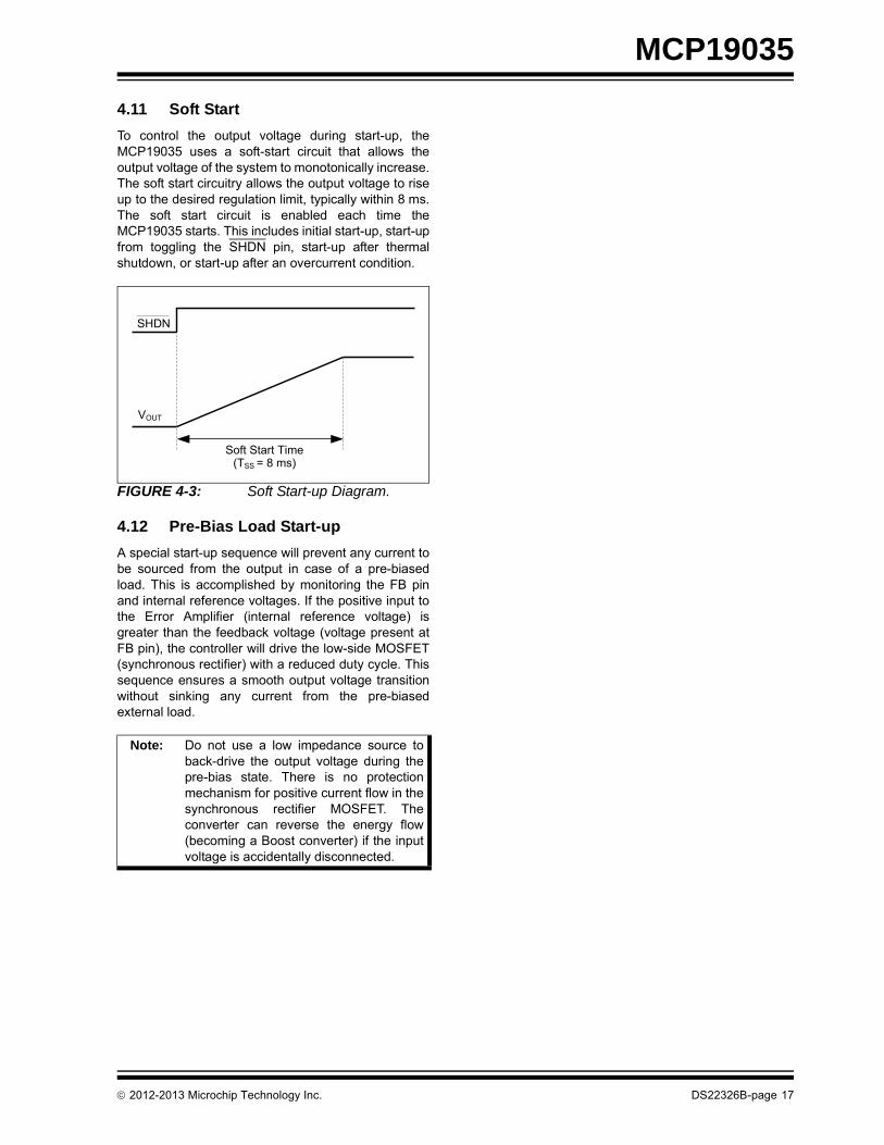
4.11 Soft Start
To control the output voltage during start-up, theMCP19035 uses a soft-start circuit that allows theoutput voltage of the system to monotonically increase.The soft start circuitry allows the output voltage to riseup to the desired regulation limit, typically within 8 ms.The soft start circuit is enabled each time theMCP19035 starts. This includes initial start-up, start-upfrom toggling the SHDN pin, start-up after thermalshutdown, or start-up after an overcurrent condition.
FIGURE 4-3: Soft Start-up Diagram.
4.12 Pre-Bias Load Start-up
A special start-up sequence will prevent any current tobe sourced from the output in case of a pre-biasedload. This is accomplished by monitoring the FB pinand internal reference voltages. If the positive input tothe Error Amplifier (internal reference voltage) isgreater than the feedback voltage (voltage present atFB pin), the controller will drive the low-side MOSFET(synchronous rectifier) with a reduced duty cycle. Thissequence ensures a smooth output voltage transitionwithout sinking any current from the pre-biasedexternal load.
Note: Do not use a low impedance source toback-drive the output voltage during thepre-bias state. There is no protectionmechanism for positive current flow in thesynchronous rectifier MOSFET. Theconverter can reverse the energy flow(becoming a Boost converter) if the inputvoltage is accidentally disconnected.
SHDN
VOUT
Soft Start Time (TSS = 8 ms)
2012-2013 Microchip Technology Inc. DS22326B-page 17

MCP19035
NOTES:
DS22326B-page 18 2012-2013 Microchip Technology Inc.
MCP19035
5.0 APPLICATION INFORMATION
5.1 Typical Applications
The MCP19035 synchronous buck controller operatesover an input voltage range up to a maximum of 30V.The output current capability depends only on theexternal MOSFET’s selection and can also be veryhigh, typically up to 20A.
Typical applications include POL modules for poweringDSPs, FPGAs and ASICs, and, in general, any step-down voltage conversion (from maximum 30V inputvoltage) for medium-to-high output current loads.
5.2 Design Procedure
To simplify this design process, an Excel®-baseddesign tool is available to support typical applications.This tool is available on the MCP19035 product website. Refer to AN1452 – “Using the MCP19035Synchronous Buck Converter Design Tool” for furtherdetails.
5.2.1 SWITCHING FREQUENCY AND THE MAXIMUM CONVERSION RATIO
The MCP19035 controller provides two options for theswitching frequency: 300 kHz and 600 kHz. In general,choosing a higher switching frequency allows the useof smaller size components (i.e. inductor and filteringcapacitors), but increases the switching losses. The300 kHz switching frequency is recommended forapplications requiring output currents up to 20A. Forapplications requiring output currents up to 10A, therecommended switching frequency is 600 kHz.
Due to the minimum “On Time” for the high-sideMOSFET driver (70 ns typical), the maximumconversion ratio must be limited to 20:1.
5.2.2 DEAD TIME SELECTION
Dead Time will affect the maximum obtainableefficiency of the converter. Selecting the Dead Timedepends on the external MOSFETs’ parameters. LowerFigure of Merit (FOM) transistors will permit the use ofshorter Dead Times. This may increase the converterefficiency by up to 2%.
Low Figure of Merit transistors allow the user to selecta low value for Dead Time (typical 12 ns) withoutcausing a shoot-through phenomenon. For low-FOMtransistors, the MCP19035 version with fixed 12 nsDead Time is recommended.
For typical medium Figure of Merit transistors, theMCP19035 version with the adaptive Dead-Timegenerator is recommended.
5.2.3 INDUCTOR SELECTION
The output inductor is responsible for smoothing thesquare wave created by the switching action and forcontrolling the output current ripple (∆IOUT). There is atrade off between efficiency and load transientresponse time when the value of the inductor ischosen. The smaller the inductance, the quicker theconverter can respond to transients in the load current.However, a smaller inductor requires a higher switchingfrequency to maintain the same level of output currentripple. Remember that increasing the switchingfrequency will also increase the switching losses in theMOSFETs.
A good compromise for the inductor current ripple is30% of the output current. The value of the inductor iscalculated in Equation 5-1:
EQUATION 5-1: INDUCTOR VALUE
The peak current in the inductor is determined inEquation 5-2:
EQUATION 5-2: INDUCTOR PEAK CURRENT
EQUATION 5-3: INDUCTOR RMS CURRENT
Additional care must be taken when selecting an induc-tor:
• Choose an inductor that has a saturation current larger than the calculated peak current. The tolerance of the inductor must also be considered (typically 20%).
• To minimize the conduction losses, choose an inductor with the lowest possible DC resistance. The maximum DC resistance specified in the data sheet will ensure the worst-case component spec-ification.
• There are many magnetic materials available for inductor core: ferrite, iron powder and composite materials. The ferrite offers the lowest core losses, but the saturation characteristic is “hard” (i.e. the inductance drops rapidly after the current reaches the saturation level). The losses of iron powder or composite material cores are higher than ferrite, but the saturation characteristic is “soft”, making it more suitable for voltage mode control converter, including the MCP19035.
L VINMAXVOUT–
VOUT
VINMAX
----------------------- 1fSW----------
10.3 IOUTMAX
------------------------------------------=
ILPEAKIOUTMAX
0.3 IOUTMAX
2------------------------------------------+=
ILRMSI
2OUT
IRipple2
3--------------------+=
2012-2013 Microchip Technology Inc. DS22326B-page 19

MCP19035
5.2.4 INPUT CAPACITOR SELECTION
The input capacitor is responsible for providing a lowimpedance voltage source for the step-down converter.This capacitor must be able to sustain high ripplecurrent, a consequence of the discontinuous inputcurrent of the buck converter. A low equivalent seriesresistance capacitor (ESR), preferably ceramic, isrecommended. For wide temperature rangeapplications, a multi-layer X7R dielectric isrecommended, while for applications with limitedtemperature range, a multi-layer X5R dielectric isacceptable. A higher ESR will produce a higher voltageripple and higher power losses. The capacitor voltagerating must be higher than the maximum operatinginput voltage of the converter.
The minimum capacitance is determined inEquation 5-4:
EQUATION 5-4: MINIMUM CAPACITANCE FOR INPUT CAPACITOR
The maximum ripple current in the input capacitoroccurs when the duty cycle is 50%. This must beconsidered worst case for calculating the inputcapacitor.
The RMS current in the input capacitor is estimatedwith Equation 5-5:
EQUATION 5-5: RMS CURRENT IN THE INPUT CAPACITOR
The input capacitor must be rated to sustain this RMScurrent without considerable losses.
5.2.5 OUTPUT CAPACITOR SELECTION
The output capacitor is responsible for smoothing theoutput voltage. It also plays an important role in thestability of the control system. The voltage ripple acrossthe output capacitor is the sum of ripple voltages due tothe Equivalent Series Resistance (ESR) and thevoltage sag due to the load current that must besupplied by the capacitor as the inductor is discharged.A low ESR capacitor, preferably ceramic, isrecommended. For wide temperature rangeapplications, a multi-layer X7R dielectric isrecommended, while for applications with limitedtemperature range, a multi-layer X5R dielectric isacceptable.
The output voltage ripple is estimated in Equation 5-6:
EQUATION 5-6: OUTPUT VOLTAGE RIPPLE
Minimum capacitance value is calculated according tothe demand of the load transient response. During atransient load current, the excessive energy stored bythe inductor must be absorbed by the output capacitoruntil the control loop sets the proper duty cycle.Equation 5-7 calculates the minimum value for theoutput capacitor value:
EQUATION 5-7: OUTPUT CAPACITOR MINIMUM VALUE
For applications that require low output voltageovershoot during a step load, the value of the outputcapacitor can become very large. In this case, it isrecommended to mix ceramic capacitors withaluminum or polymer electrolytic capacitors to reachthe recommended value.
CIN_MIN
IOUT D 1 D– fSW VRipple D IOUT ESR– -----------------------------------------------------------------------------------=
Where:
CIN_MIN = Minimum Capacitance of the Input Capacitor (in Farad)
IOUT = Output Current (A)
D = Duty Cycle (for worst case this is 0.5)
fSW = Switching Frequency (Hz)
VRipple = Input Voltage Ripple (usually between 0.1V and 0.5V)
ESR = Equivalent Series Resistance of the Capacitor (in Ohm)
IRMS CIN IOUT
IRipple
12----------------+
DVOUT IOUT
VIN-------------------------------- –=
VRipple IRipple ESR1
8 COUT fSW--------------------------------------+
=
Where:
IRipple = Inductor Current Ripple (A)
VRipple = Output Voltage Ripple (V)
COUT = Output Capacitor (F)
ESR = Equivalent Series Resistance of the Output Capacitor (Ohm)
COUT
L IOH2
IOL2–
Vf2
VOUT2–
------------------------------------=
Where:
IOH = Final Value of the Output Current
IOL = Initial Value of the Output Current
VOUT = Initial Output Voltage
Vf = Final Output Voltage
DS22326B-page 20 2012-2013 Microchip Technology Inc.
MCP19035
5.2.6 MOSFETS SELECTION
Choosing the right MOSFET is a critical part of thedesign for a switching regulator. Their performance willdirectly impact the efficiency and reliability of theregulator.
The MCP19035 synchronous buck controller offers anintegrated, logic-level MOSFET driver, and is capableof supplying 5V to drive the MOSFET gates. As aresult, logic-level MOSFETs must be used. SuitableMOSFETs should meet the requirement of voltage andcurrent rating.
A key parameter for evaluating the MOS transistorperformance is the Figure of Merit. For a givenMOSFET, this is defined as the product between theTotal Gate Charge (QG) and RDS(ON) (see Equation 5-8).
EQUATION 5-8: FIGURE OF MERIT
A lower FOM value means a higher-performance MOStransistor.
For the high-side MOSFET, power losses consist ofboth switching and conduction losses. Conductionlosses are high when the duty cycle of the converter ishigh. The conduction loss of the high-side MOSFETcan be estimated by multiplying the RDS(ON) with theRMS value of the current that passes through the tran-sistor (see Equation 5-9).
EQUATION 5-9: RMS VALUE FOR HIGH-SIDE CURRENT
The conduction losses for high-side MOS transistor areestimated in Equation 5-10:
EQUATION 5-10: CONDUCTION LOSSES FOR HIGH-SIDE MOSFET
The switching losses are more difficult to calculate,since they depend on many parameters. Equation 5-11shows an estimation of these losses:
EQUATION 5-11: SWITCHING LOSSES FOR HIGH-SIDE MOSFET
The ts(HL) and ts(LH) times can be estimated using thefollowing equations:
EQUATION 5-12:
The total power losses for the high-side MOSFET canbe calculated with Equation 5-13:
EQUATION 5-13: TOTAL POWER LOSSES FOR HIGH-SIDE MOSFET
For applications that operate with low duty cycle (lowerthan 30%) or high input voltage, the power losses forthe high-side transistor are mainly switching losses.For these applications, it is recommended to choose aMOSFET that offers a low Total Gate Charge.
For applications that operate with duty cycles higherthan 50%, the power losses for the high-side transistorare mainly conduction losses. For these applications,choose a MOSFET that has a low RDS(on).
FOM QG Tot RDS ON =
IRMS High-Side D IOUT2 IRipple
2
12----------------+
=
Where:
D = Duty Cycle
IOUT = Output Current (A)
IRipple = Current Ripple in the Inductor (typically 30% of the maximum output current) (A)
PCOND High-Side IRMS High-Side2 RDS on HS max =
PSW High-Side
VIN IOUT2
--------------------------- ts HL ts LH + fSW=
Where:
VIN = Input Voltage (V)
IOUT = Output Current (A)
fSW = Switching Frequency (Hz)
ts(HL) = MOSFET Switching Time (High-to-Low transition) (s)
ts(LH) = MOSFET Switching Time (Low-to-High transition) (s)
ts HL QG Total
IDRVSink
----------------------=
ts LH QG Total
IDRVSource
----------------------=
Where:
QG(Total) = High-side MOSFET Total Gate Charge
IDRVSink = Sink Peak Current for High-Side Driver (typical 1A)
IDRVSource = Source Peak Current for High-Side Driver (typical 1A)
PLoss High-Side PCOND High-Side PSW High-Side+=
2012-2013 Microchip Technology Inc. DS22326B-page 21

MCP19035
The low-side MOSFET (synchronous rectifier) is “soft-commutated” by the energy stored in the inductor , thusreducing the switching losses. For the low-side transis-tor, the power losses mainly consist of conductionlosses, body diode conduction losses and body diodereverse recovery losses.
Similarly to the high-side, the RMS current that passthrough the low-side MOSFET is calculated usingEquation 5-14:
EQUATION 5-14: RMS CURRENT FOR LOW-SIDE MOSFET
The conduction losses for low-side MOS transistor areestimated in Equation 5-15:
EQUATION 5-15: CONDUCTION LOSSES FOR LOW-SIDE TRANSISTOR
The body diode conduction loss is calculated inEquation 5-16:
EQUATION 5-16: BODY DIODE CONDUCTION LOSSES
The body diode recovery time losses will be calculatedusing Equation 5-17:
EQUATION 5-17: BODY DIODE REVERSE RECOVERY LOSSES
The total power loss for the low-side MOSFET can nowbe estimated by summing the power losses inEquation 5-18:
EQUATION 5-18: TOTAL POWER LOSS FOR LOW-SIDE MOSFET (SR)
The conduction losses are the dominant part of the totallosses for the low-side transistor; choose a MOSFETwith a low RDS(on).
The body diode conduction and reverse recoverylosses can be greatly minimized by reducing the DeadTimes necessary to prevent the shoot-through. Thiscan be achieved by choosing transistors that have avery low Figure of Merit (FOM) MOSFET for both sides.
5.2.7 BOOTSTRAP CAPACITOR SELECTION
The selection of the bootstrap capacitor is based uponthe total gate charge of the high-side power MOSFETand the allowable droop in gate drive voltage while thehigh-side power MOSFET is conducting (seeEquation 5-19).
EQUATION 5-19: BOOTSTRAP CAPACITOR
It is recommended that the voltage droop does notexceed 50 mV. A low ESR, ceramic capacitor, rated atleast 16 VDC, is recommended.
IRMS Low-Side 1 D– IOUT2 IRipple
2
12----------------+
=
Where:
D = Duty Cycle
IOUT = Output Current (A)
IRipple = Current Ripple in the Inductor (typically 30% of the maximum output current) (A)
PCOND Low-Side IRMS Low-Side2 RDS on LS max =
PLOSS BD IOUT VF tBD fSW=
Where:
VF = Forward Voltage of the Body Diode (V)
tBD = Total Conduction Time for Body Diode (s)
PRR
QRR VIN fSW2
----------------------------------------=
Where:
QRR = Reverse Recovery Charge of the Body Diode (C)
PLoss Low-Side PCOND Low-Side PLOSS BD PRR+ +=
CBOOT
QG Total
VDROOP------------------------=
Where:
QG(Total) = High-side MOSFET Total Gate Charge (C)
∆VDROOP = Allowable Gate Drive Voltage Droop (V)
DS22326B-page 22 2012-2013 Microchip Technology Inc.
MCP19035
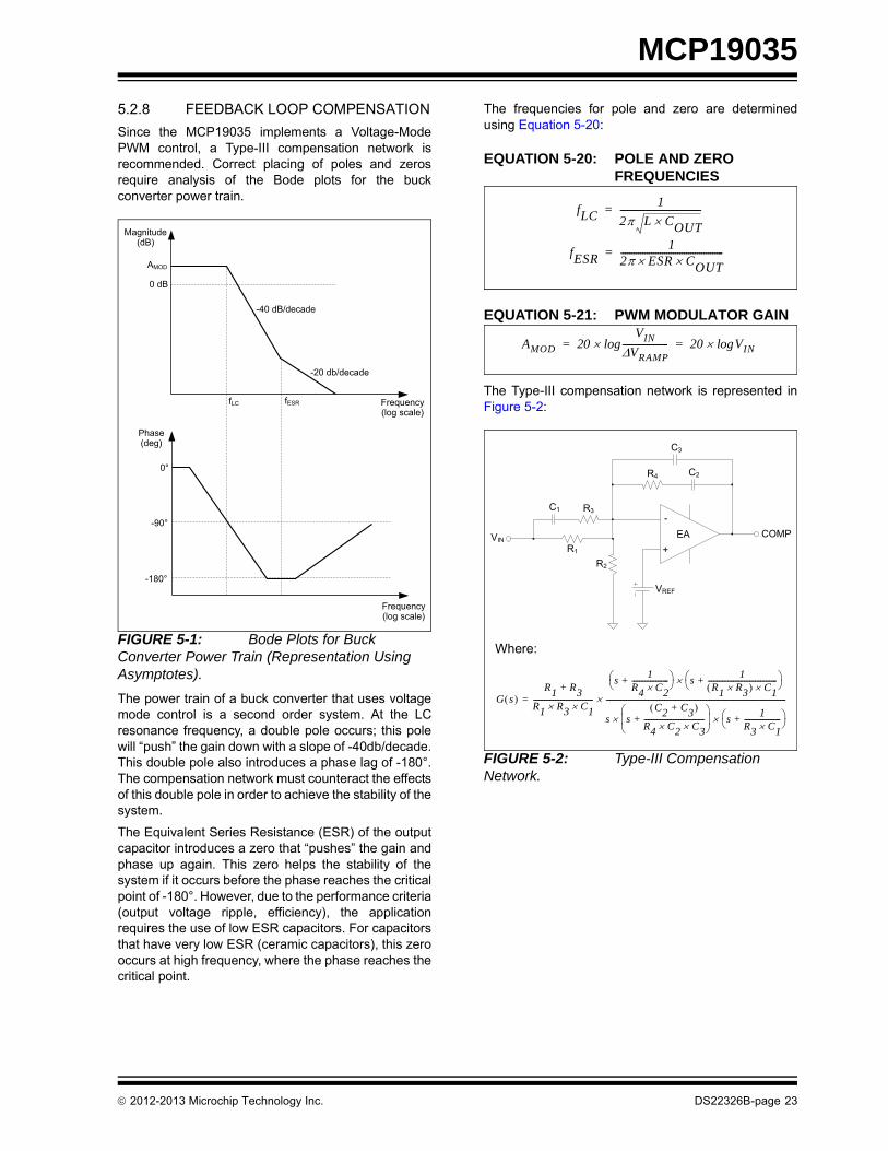
5.2.8 FEEDBACK LOOP COMPENSATION
Since the MCP19035 implements a Voltage-ModePWM control, a Type-III compensation network isrecommended. Correct placing of poles and zerosrequire analysis of the Bode plots for the buckconverter power train.
FIGURE 5-1: Bode Plots for Buck Converter Power Train (Representation Using Asymptotes).
The power train of a buck converter that uses voltagemode control is a second order system. At the LCresonance frequency, a double pole occurs; this polewill “push” the gain down with a slope of -40db/decade.This double pole also introduces a phase lag of -180°.The compensation network must counteract the effectsof this double pole in order to achieve the stability of thesystem.
The Equivalent Series Resistance (ESR) of the outputcapacitor introduces a zero that “pushes” the gain andphase up again. This zero helps the stability of thesystem if it occurs before the phase reaches the criticalpoint of -180°. However, due to the performance criteria(output voltage ripple, efficiency), the applicationrequires the use of low ESR capacitors. For capacitorsthat have very low ESR (ceramic capacitors), this zerooccurs at high frequency, where the phase reaches thecritical point.
The frequencies for pole and zero are determinedusing Equation 5-20:
EQUATION 5-20: POLE AND ZERO FREQUENCIES
EQUATION 5-21: PWM MODULATOR GAIN
The Type-III compensation network is represented inFigure 5-2:
FIGURE 5-2: Type-III Compensation Network.
Magnitude(dB)
Frequency(log scale)
AMOD
0 dB
-40 dB/decade
-20 db/decade
fLC fESR
Phase(deg)
0°
-90°
-180°
Frequency(log scale)
fLC1
2 L COUT-------------------------------------=
fESR1
2 ESR COUT-----------------------------------------------=
AMOD 20VIN
VRAMP---------------------log 20 VINlog= =
G s R1 R3+
R1 R3 C1---------------------------------
s1
R4 C2--------------------+
s1
R1 R3 C1--------------------------------------+
s sC2 C3+
R4 C2 C3---------------------------------+
s1
R3 C1--------------------+
---------------------------------------------------------------------------------------------------=
Where:
C1 R3
C3
R1
R2
C2
VREF
R4
+
-EAVIN
COMP
2012-2013 Microchip Technology Inc. DS22326B-page 23
MCP19035
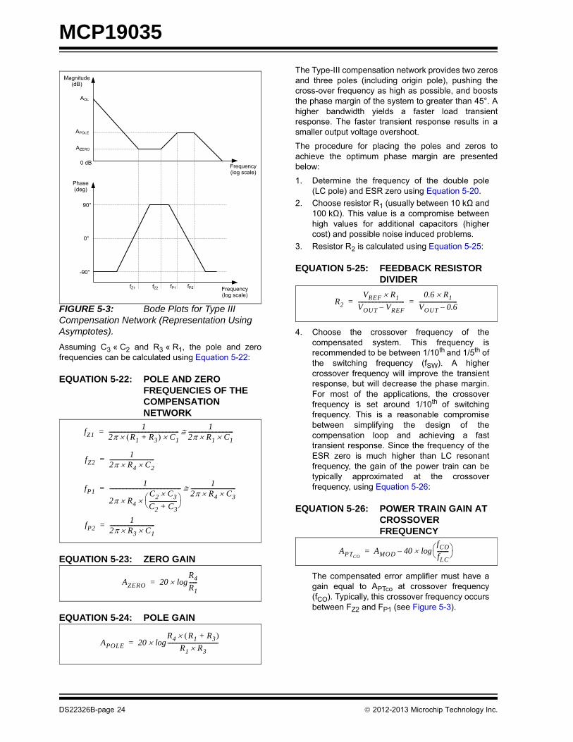
FIGURE 5-3: Bode Plots for Type III Compensation Network (Representation Using Asymptotes).
Assuming C3 « C2 and R3 « R1, the pole and zerofrequencies can be calculated using Equation 5-22:
EQUATION 5-22: POLE AND ZERO FREQUENCIES OF THE COMPENSATION NETWORK
EQUATION 5-23: ZERO GAIN
EQUATION 5-24: POLE GAIN
The Type-III compensation network provides two zerosand three poles (including origin pole), pushing thecross-over frequency as high as possible, and booststhe phase margin of the system to greater than 45°. Ahigher bandwidth yields a faster load transientresponse. The faster transient response results in asmaller output voltage overshoot.
The procedure for placing the poles and zeros toachieve the optimum phase margin are presentedbelow:
1. Determine the frequency of the double pole(LC pole) and ESR zero using Equation 5-20.
2. Choose resistor R1 (usually between 10 kΩ and100 kΩ). This value is a compromise betweenhigh values for additional capacitors (highercost) and possible noise induced problems.
3. Resistor R2 is calculated using Equation 5-25:
EQUATION 5-25: FEEDBACK RESISTOR DIVIDER
4. Choose the crossover frequency of thecompensated system. This frequency isrecommended to be between 1/10th and 1/5th ofthe switching frequency (fSW). A highercrossover frequency will improve the transientresponse, but will decrease the phase margin.For most of the applications, the crossoverfrequency is set around 1/10th of switchingfrequency. This is a reasonable compromisebetween simplifying the design of thecompensation loop and achieving a fasttransient response. Since the frequency of theESR zero is much higher than LC resonantfrequency, the gain of the power train can betypically approximated at the crossoverfrequency, using Equation 5-26:
EQUATION 5-26: POWER TRAIN GAIN AT CROSSOVER FREQUENCY
The compensated error amplifier must have again equal to APTco at crossover frequency(fCO). Typically, this crossover frequency occursbetween FZ2 and FP1 (see Figure 5-3).
Magnitude(dB)
Frequency(log scale)
AOL
0 dB
fZ1 fZ2
Phase(deg)
0°
90°
-90°
Frequency(log scale)
fP1 fP2
APOLE
AZERO
fZ11
2 R1 R3+ C1--------------------------------------------------
12 R1 C1--------------------------------=
fZ21
2 R4 C2--------------------------------=
fP11
2 R4
C2 C3C2 C3+--------------------
---------------------------------------------------1
2 R4 C3--------------------------------=
fP21
2 R3 C1--------------------------------=
AZERO 20R4
R1------log=
APOLE 20R4 R1 R3+
R1 R3------------------------------------log=
R2
VREF R1VOUT VREF–---------------------------------
0.6 R1VOUT 0.6–---------------------------= =
APTCOAMOD 40–
fCO
fLC-------- log=
DS22326B-page 24 2012-2013 Microchip Technology Inc.
MCP19035
5. The first zero of the compensation network mustbe placed at the fLC frequency. The capacitor C1is calculated using Equation 5-27:
EQUATION 5-27: CAPACITOR C1
6. The value of the resistor R4 is estimated usingEquation 5-28:
EQUATION 5-28: RESISTOR R4
7. The second zero of the compensation networkmust be placed at half of the fLC frequency. Thevalue of the capacitor C2 is calculated inEquation 5-29:
EQUATION 5-29: CAPACITOR C2
8. The first pole of the compensation network mustbe placed at fSW. The value of C3 is calculated inEquation 5-30:
EQUATION 5-30: CAPACITOR C3
9. The second pole of the compensation networkmust be placed at half of the fSW .The value forresistor R3 is calculated in Equation 5-31:
EQUATION 5-31: RESISTOR R3
The compensation circuit can be simulated with anyavailable simulator. The values of the components canbe adjusted to meet the initial design parameters(crossover frequency and phase margin). It is also nec-essary to ensure that the gain of the compensation cir-cuit does not exceed the gain of the error amplifier. Dueto the interactions between poles and zeros, it is highlyrecommended to use the design tool provided byMicrochip Technology Inc. to design and analyze thecompensation network.
C1
L COUTR1
----------------------------=
R4
fCO
fLC--------
1VIN-------- R1=
Where:
fCO = cross-over frequency for the compensated system (usually 1/10th of fSW)
C2 2L COUT
R4----------------------------=
C31
2 R4 fSW------------------------------------------=
R31
C1 fSW---------------------------------=
2012-2013 Microchip Technology Inc. DS22326B-page 25
MCP19035
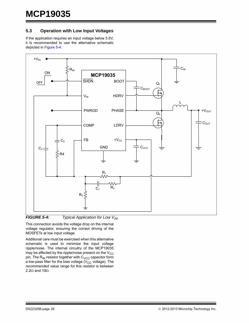
5.3 Operation with Low Input Voltages
If the application requires an input voltage below 5.5V,it is recommended to use the alternative schematicdepicted in Figure 5-4.
FIGURE 5-4: Typical Application for Low VIN.
This connection avoids the voltage drop on the internalvoltage regulator, ensuring the correct driving of theMOSFETs at low input voltage.
Additional care must be exercised when this alternativeschematic is used to minimize the input voltageripple/noise. The internal circuitry of the MCP19035may be affected by the ripple/noise present on the VCCpin. The RIN resistor together with CVCC capacitor forma low-pass filter for the bias voltage (VCC voltage). Therecommended value range for this resistor is between2.2 and 10.
CIN
COUT
L
Q1
Q2
MCP19035
HDRV
LDRV
PHASE
BOOT
+VCC
CBOOT
CVCC
+VOUT
SHDN
VIN
PWRGD
COMP
FB
R1
R3C1
R2
C3
R4
C2
+VIN
ON
OFF
RIN
GND
DS22326B-page 26 2012-2013 Microchip Technology Inc.
MCP19035
6.0 DESIGN EXAMPLE
This example illustrates the step-by-step design proce-dure for a 12V to 1.8V synchronous buck converterusing the MCP19035 controller. To minimize the designeffort, Microchip provides a design tool that is used tocalculate the component values. See AN1452 - “Usingthe MCP19035 Synchronous Buck Converter DesignTool” for further details (DS01452).
The electrical parameters are detailed in Table 6-1.
6.0.1 INDUCTOR SELECTION
The inductor must be sized for a typical ripple currentthat is around 30% of maximum output current. Theinductor value calculated with Equation 5-1 is 1.16 µH.To compensate against component tolerance, choosethe next higher standard value 1.5 µH (typically 20% forhigh current inductors).
The peak current in the inductor can be calculated withEquation 5-2, its value being 17.25A. The inductormust sustain, without saturating, this peak current. Tomaintain low-conduction losses, the DC resistance ofthe inductor must be as low as possible. Table 6-2shows some suitable inductors for this application.
TABLE 6-1: DESIGN EXAMPLE ELECTRICAL SPECIFICATION
Parameter Test Conditions Min Nominal Max Unit
Input Voltage (VIN) 8 12 14 V
Output Voltage (VOUT) 0 IOUT 15A — 1.8 — V
Line Regulation 8.0V VIN 14V — — 0.5 %
Load Regulation 0A IOUT 15A — — 0.5 %
Output ripple (VOUT_RIPPLE) IOUT = 15A — — 30 mV
Input ripple (VIN_RIPPLE) IOUT = 15A — — 0.3 V
Output overshoot Step from 3.75A to 11.25A — — 100 mV
Output undershoot Step from 11.25A to 3.75A — — 100 mV
Output current (IOUT) 0 — 15 A
Efficiency VIN = 12V, IOUT = 10A 90 — — %
TABLE 6-2: SUITABLE INDUCTORS FROM VARIOUS VENDORS
Vendor Part NumberInductance
(µH)DCR(m)
ISAT(A)
Coilcraft® XAL1010-152MEB 1.5 1.76 36.6
Wurth Elektronik® 7443320150 1.5 2.1 27
TDK - EPC® B82559A0142A013 1.4 1.5 22
Bourns® SRP1270-1R5M 1.5 2.1 48
2012-2013 Microchip Technology Inc. DS22326B-page 27

MCP19035
6.0.2 INPUT CAPACITOR SELECTION
The converter operates with a maximum duty cycle of22.5%. A ceramic capacitor (X7R dielectric) with a10 m ESR (typical) will be used. The minimumcapacitance for input capacitor, calculated inEquation 5-4, is 32.7 µF. Use two standard 22 µFcapacitors (X7R) rated at 25VDC in parallel.
6.0.3 OUTPUT CAPACITOR SELECTION
Based on a step load from 25% to 75% of the maximumoutput current, the minimum value for the output capac-itor can be determined with Equation 5-7. The mini-mum value is 456 µF. Choose the next higher standardvalue (500 µF). The ESR of the output capacitor willstrongly affect the output voltage ripple. Use five100 µF standard ceramic capacitors (X7R or X5Rdielectric) rated at 6.3VDC in parallel. The estimatedfinal value of the ESR is lower than 5 m. The outputvoltage ripple is now estimated with Equation 5-6.
6.0.4 MOSFETS SELECTION
Before the MOSFET selection, the total losses of theconverter should be estimated. For this application, theinput power can be estimated using Equation 6-1:
EQUATION 6-1: INPUT POWER
The total power losses are estimated in Equation 6-2:
EQUATION 6-2: TOTAL CONVERTER LOSSES
To achieve the efficiency goal (90%), the total powerlosses must be lower than 2W at 10A output current.Table 6-3 shows how these losses are distributed overthe converter components. The power losses distribu-tion varies with the design parameters. As a rule ofthumb, for designs that have higher conversion ratio(low duty cycles), the losses for the high-side MOSFETare mainly switching losses. For the low side, most ofthe losses will be the conduction losses.
An important part of the total power losses (over 75%)are dissipated by the MOSFETs.
For the high-side MOSFET, the total amount of losses(conduction and switching losses) should not exceed0.72W. This design has a higher conversion ratio(greater than 7:1), thus most of the losses of the high-side MOSFET will be switching losses. As a rule ofthumb, the switching losses will be considered to be70% of the total losses.
The conduction losses for the high-side MOSFET areestimated in Equation 5-10. High-side MOSFETconduction losses are high at low input voltages. Themaximum RDS(on) for the high-side MOSFET is:
EQUATION 6-3: MAXIMUM HIGH-SIDE RDS(ON)
For this design, where IRMS High-Side = 3.9A at 12Vinput voltage and 10A output current, the high-sideMOSFET should have a RDS(On) lower than 14 mΩ.
For the high-side MOSFET, most of the losses areswitching losses (70%). The maximum total gatecharge for the high-side MOSFET is:
EQUATION 6-4: MAXIMUM TOTAL GATE CHARGE FOR THE HIGH-SIDE MOSFET
The maximum Total Gate Charge (QG(Total)) at 4.5VVGS should be lower than 12 nC (calculated for 10Aoutput current).
PIN
UOUT IOUTmaxEff
------------------------------------------=
PLOSS PIN POUT–=
TABLE 6-3: ESTIMATION OF THE POWER LOSSES DISTRIBUTION
Component Losses (%)
High-Side MOSFET 36
Low-Side MOSFET 40
Inductor 10
Input Capacitor 2
Output Capacitor 1
PWM Controller 10
Traces DC Resistance 1
RDS on PLOSS High Side–
IRMS High Side–2
----------------------------------------- 0.3=
QG Total PLOSS High Side–
VIN Max IOUT fSW------------------------------------------------------- 0.7=
DS22326B-page 28 2012-2013 Microchip Technology Inc.
MCP19035
For the low-side MOSFET, losses are mainlyconduction losses. As a rule of thumb, the conductionlosses are considered to be 85% of the total losses. Forthis design, the maximum power losses (estimated at12V input voltage and 10A output current) for low-sideshould be lower than 0.9W. Estimate the maximumRDS(On) for the low-side MOSFET using Equation 6-5:
EQUATION 6-5: MAXIMUM RD(ON) OF LOW-SIDE MOSFET
In this design, IRMS Low-Side = 9.3A at 12V inputvoltage, 10A output current and the maximum RDS(On)for low-side MOSFET = 7.8 m.
For this design, Microchip's MCP87050 andMCP87022 high-performance MOSFETs can be used.Calculate the total losses introduced by these transis-tors using the provided equations. For the high-sideMOSFET (MCP87050), the total loss is 0.66W. Thelow-side MOSFET (MCP87022) will dissipate a 0.3Wloss.
6.0.5 BOOTSTRAP CAPACITOR SELECTION
From Equation 5-19, the value of the BootstrapCapacitor should be higher than 276 nF. Choose thestandard value 330 nF ceramic capacitor (X7R) ratedat 16 VDC.
6.0.6 DEAD TIME (DT) SELECTION
The MOSFET used in this design has a low Figure ofMerit parameter. The overall efficiency of the convertercan be improved by choosing the MCP19035 withoptimized Dead Time.
6.0.7 OVERCURRENT PROTECTION THRESHOLDS
The MCP19035 controller provides two fixed thresholdfor high and low-side overcurrent protection circuits.These thresholds are 480 mV (typical) for high-sideand 180 mV (typical) for the low-side. The peak currentfor the high-side is:
EQUATION 6-6: MAXIMUM PEAK CURRENT FOR A HIGH-SIDE MOSFET
For this design, the maximum peak current that flowsinto the high-side MOSFET is 87A.
The peak current for the low-side MOSFET is:
EQUATION 6-7: MAXIMUM PEAK CURRENT FOR A LOW-SIDE MOSFET
For this design, the maximum peak current that flowsinto the low-side MOSFET is 81A.
6.0.8 FEEDBACK LOOP COMPENSATION
For this design, the crossover frequency is 30 kHz,while the resonant frequency of LC tank is 5.88 kHz.With these parameters, and following the designprocedure described in Section 5.2, DesignProcedure, the value for compensation networkcomponents can be calculated.
The components used for the compensation networkmust be of good quality and tolerance. Therecommended dielectric for capacitors is C0G and thetolerance 5%. The recommended tolerance forresistors is 1%.
6.0.9 LAYOUT RECOMMENDATIONS
Good printed circuit board layout techniques areimportant to any switching circuitry, and switchingpower supplies are no different. Here are the guidelinesfor the PCB layout:
• The exposed pad of MCP19035 DFN case is the only connection to the internal device ground. Connect this pad directly to the board ground plane.
• Place at least four vias in the exposed pad land to help remove heat from the device.
• Use separate grounds for power and signal paths. Keep high current paths away from sensitive components and nodes (ex. feedback and compensation network components).
• Four layer PCBs are highly recommended to obtain optimum results regarding noise/EMI. Use an internal layer as ground plane.
RDS on PLOSS Low Side–
IRMS Low Side–2
---------------------------------------- 0.85=
IMAXHS
0.48RDS on HS-------------------------=
TABLE 6-4: COMPENSATION NETWORK COMPONENTS
Component Value Standard Value
R1 20 k 20 k
R2 10 k 10 k
R3 0.774 k 0.75 k
R4 8.6 k 8.2 k
C1 1.37 nF 1.2 nF
C2 6.36 nF 6.8 nF
C3 61 pF 68 pF
IMAXLS
0.18RDS on LS------------------------=
2012-2013 Microchip Technology Inc. DS22326B-page 29
MCP19035
• For double layer boards, a single ground plane (usually the bottom) is recommended.
• Use short, wide traces for the MOSFET’s gate drive connection (LDRV and HDRV signals).
• Place the main MOSFET (control/high-side MOS-FET) as close as possible to the input capacitors.
• Minimize the connections between MOSFETs, the inductor and the MCP19035 case (PHASE node). Place this node over a ground plane to minimize the radiated noise.
• Place the compensation network components
near the MCP19035 case and connect these components to a low noise ground (signal ground).
• Locate the VIN decoupling capacitor close to the MCP19035 case.
• Locate the Bootstrap Circuit capacitor close to the MCP19035 case.
• Minimize the area of high frequency current loops.
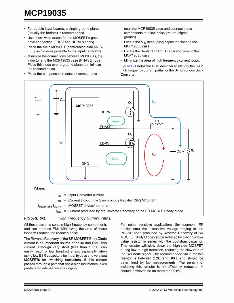
Figure 6-1 helps the PCB designer to identify the mainhigh frequency current paths for the Synchronous BuckConverter.
FIGURE 6-1: High Frequency Current Paths.
All these currents contain high-frequency componentsand can produce EMI. Minimizing the area of theseloops will reduce the radiated noise.
The Reverse Recovery of the SR MOSFET Body Diodecurrent is an important source of noise and EMI. Thiscurrent, although very short (less than 10 ns), caneasily reach a few hundred amps, especially whenusing low ESR capacitors for input bypass and very fastMOSFETs for switching transistors. If this currentpasses through a path that has a high inductance, it willproduce an intense voltage ringing.
For noise sensitive applications (for example, RFapplications) the excessive voltage ringing in thePHASE node produced by Reverse Recovery of SRMOSFET Body Diode can be reduced by placing a low-value resistor in series with the bootstrap capacitor.This resistor will slow down the high-side MOSFETduring low-to-high transition, reducing the slew rate ofthe SW node signal. The recommended value for thisresistor is between 2.2Ω and 10Ω, and should bedetermined by lab measurements. The penalty ofincluding this resistor is an efficiency reduction. Itshould, however, be no more than 0.5%.
CIN
COUT
L1
Q1
Q2
RL
MCP19035
HDRV
LDRV
PHASE
IIN
ISR
IHDRV
ILDRV
IRR
GND
Where:
IIN = Input Converter current
ISR = Current through the Synchronous Rectifier (SR) MOSFET
IHDRV and ILDRV = MOSFET drivers’ currents
IRR = Current produced by the Reverse Recovery of the SR MOSFET body diode
DS22326B-page 30 2012-2013 Microchip Technology Inc.
MCP19035
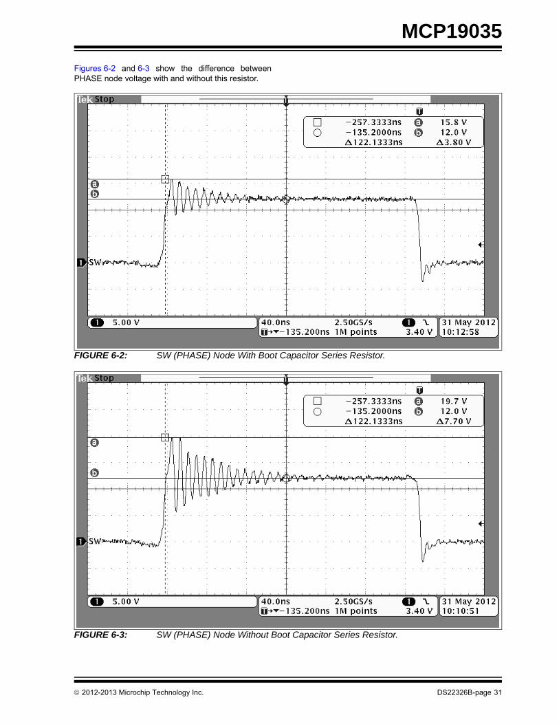
Figures 6-2 and 6-3 show the difference betweenPHASE node voltage with and without this resistor.
FIGURE 6-2: SW (PHASE) Node With Boot Capacitor Series Resistor.
FIGURE 6-3: SW (PHASE) Node Without Boot Capacitor Series Resistor.
2012-2013 Microchip Technology Inc. DS22326B-page 31
MC
P19035
DS
22
32
6B
-pa
ge
32
2
01
2-2
01
3 M
icroch
ip T
ech
no
log
y Inc.
100FC7
100FC8
100FC9
12
J2VOUT
100FC5
100FC6
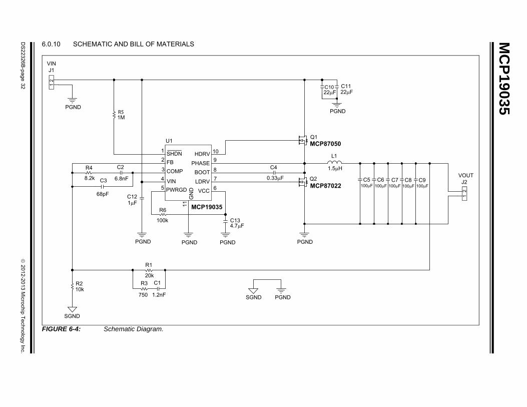
6.0.10 SCHEMATIC AND BILL OF MATERIALS
FIGURE 6-4: Schematic Diagram.
SHDN1
FB2
COMP3
VIN4
PWRGD5 VCC 6LDRV 7BOOT 8
PHASE 9HDRV 10
GN
D11
U1
MCP19035
Q1MCP87050
Q2MCP87022
PGND PGNDPGND
SGND
PGNDPGND
SGND PGND
PGND
1.5H
L1
10kR2
1MR5
6.8nF
C2
20k
R1
22FC10
22FC11
4.7FC13
1FC12
12
J1
1.2nF
C1
750
R3
8.2k
R4
68pF
C3
VIN
100k
R6
0.33F
C4
MCP19035
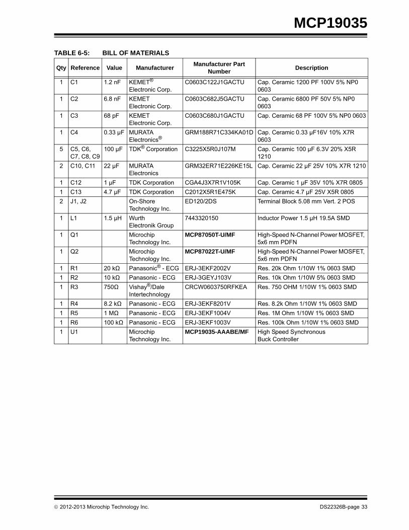
TABLE 6-5: BILL OF MATERIALS
Qty Reference Value ManufacturerManufacturer Part
NumberDescription
1 C1 1.2 nF KEMET® Electronic Corp.
C0603C122J1GACTU Cap. Ceramic 1200 PF 100V 5% NP0 0603
1 C2 6.8 nF KEMETElectronic Corp.
C0603C682J5GACTU Cap. Ceramic 6800 PF 50V 5% NP0 0603
1 C3 68 pF KEMETElectronic Corp.
C0603C680J1GACTU Cap. Ceramic 68 PF 100V 5% NP0 0603
1 C4 0.33 µF MURATA Electronics®
GRM188R71C334KA01D Cap. Ceramic 0.33 µF16V 10% X7R 0603
5 C5, C6, C7, C8, C9
100 µF TDK® Corporation C3225X5R0J107M Cap. Ceramic 100 µF 6.3V 20% X5R 1210
2 C10, C11 22 µF MURATA Electronics
GRM32ER71E226KE15L Cap. Ceramic 22 µF 25V 10% X7R 1210
1 C12 1 µF TDK Corporation CGA4J3X7R1V105K Cap. Ceramic 1 µF 35V 10% X7R 0805
1 C13 4.7 µF TDK Corporation C2012X5R1E475K Cap. Ceramic 4.7 µF 25V X5R 0805
2 J1, J2 On-Shore Technology Inc.
ED120/2DS Terminal Block 5.08 mm Vert. 2 POS
1 L1 1.5 µH Wurth Electronik Group
7443320150 Inductor Power 1.5 µH 19.5A SMD
1 Q1 Microchip Technology Inc.
MCP87050T-U/MF High-Speed N-Channel Power MOSFET, 5x6 mm PDFN
1 Q2 Microchip Technology Inc.
MCP87022T-U/MF High-Speed N-Channel Power MOSFET, 5x6 mm PDFN
1 R1 20 kΩ Panasonic® - ECG ERJ-3EKF2002V Res. 20k Ohm 1/10W 1% 0603 SMD
1 R2 10 kΩ Panasonic - ECG ERJ-3GEYJ103V Res. 10k Ohm 1/10W 5% 0603 SMD
1 R3 750Ω Vishay®/Dale Intertechnology
CRCW0603750RFKEA Res. 750 OHM 1/10W 1% 0603 SMD
1 R4 8.2 kΩ Panasonic - ECG ERJ-3EKF8201V Res. 8.2k Ohm 1/10W 1% 0603 SMD
1 R5 1 MΩ Panasonic - ECG ERJ-3EKF1004V Res. 1M Ohm 1/10W 1% 0603 SMD
1 R6 100 kΩ Panasonic - ECG ERJ-3EKF1003V Res. 100k Ohm 1/10W 1% 0603 SMD
1 U1 Microchip Technology Inc.
MCP19035-AAABE/MF High Speed Synchronous Buck Controller
2012-2013 Microchip Technology Inc. DS22326B-page 33

MCP19035
NOTES:
DS22326B-page 34 2012-2013 Microchip Technology Inc.
MCP19035
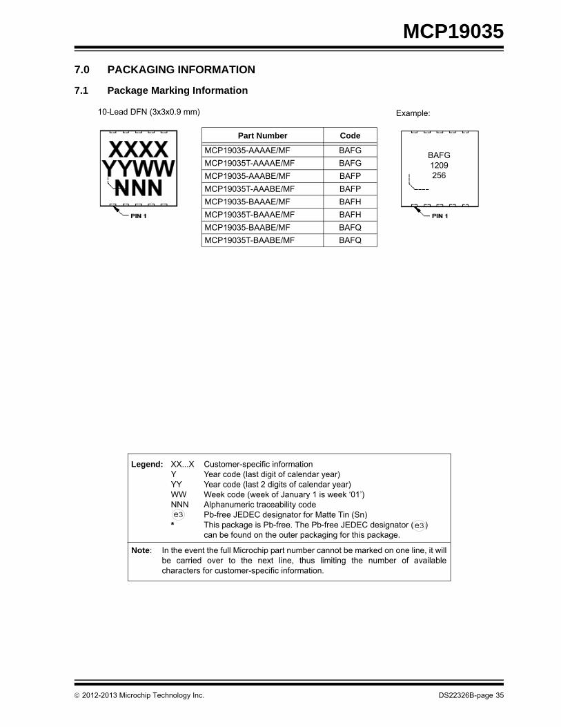
7.0 PACKAGING INFORMATION
7.1 Package Marking Information
Legend: XX...X Customer-specific informationY Year code (last digit of calendar year)YY Year code (last 2 digits of calendar year)WW Week code (week of January 1 is week ‘01’)NNN Alphanumeric traceability code Pb-free JEDEC designator for Matte Tin (Sn)* This package is Pb-free. The Pb-free JEDEC designator ( )
can be found on the outer packaging for this package.
Note: In the event the full Microchip part number cannot be marked on one line, it willbe carried over to the next line, thus limiting the number of availablecharacters for customer-specific information.
3e
3e
Part Number Code
MCP19035-AAAAE/MF BAFG
MCP19035T-AAAAE/MF BAFG
MCP19035-AAABE/MF BAFP
MCP19035T-AAABE/MF BAFP
MCP19035-BAAAE/MF BAFH
MCP19035T-BAAAE/MF BAFH
MCP19035-BAABE/MF BAFQ
MCP19035T-BAABE/MF BAFQ
BAFG1209256
10-Lead DFN (3x3x0.9 mm) Example:
2012-2013 Microchip Technology Inc. DS22326B-page 35
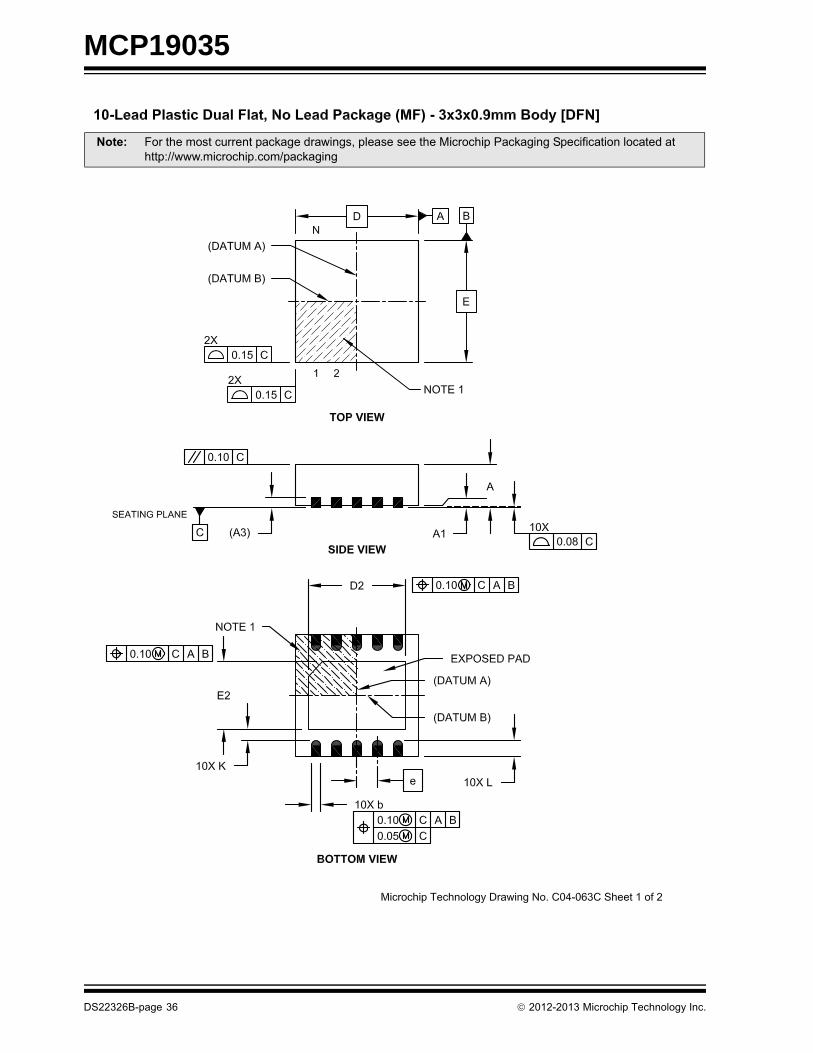
MCP19035
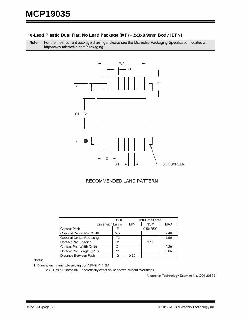
Note: For the most current package drawings, please see the Microchip Packaging Specification located at http://www.microchip.com/packaging
DS22326B-page 36 2012-2013 Microchip Technology Inc.
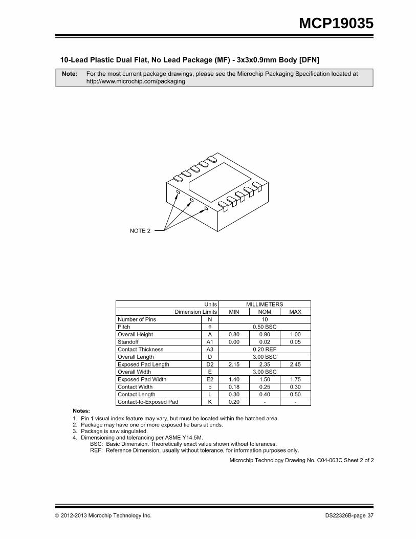
MCP19035
Note: For the most current package drawings, please see the Microchip Packaging Specification located at http://www.microchip.com/packaging
2012-2013 Microchip Technology Inc. DS22326B-page 37
MCP19035
Note: For the most current package drawings, please see the Microchip Packaging Specification located at http://www.microchip.com/packaging
DS22326B-page 38 2012-2013 Microchip Technology Inc.
MCP19035
APPENDIX A: REVISION HISTORY
Revision B (March 2013)
The following is the list of modifications:
1. Added the 600 kHz option Switching Frequencyparameter and related information throughoutthe document.
2. Updated the DC Electrical Characteristics tableto reflect the 600 kHz option for the SwitchingFrequency parameter.
3. Updated Figure 2-1, Figure 2-3, and Figure 2-10.
4. Updated Section 4.4 “Internal Oscillator”.
5. Updated the Switching Frequency value inEquation 4-1.
6. Updated Section 4.11 “Soft Start”.
7. Updated Figure 4-3.
8. Added a note to Section 4.12 “Pre-Bias LoadStart-up”.
9. Updated Section 5.2.1 “Switching Frequencyand the Maximum Conversion Ratio”.
10. Updated Section 7.1 “Package Marking Infor-mation” with the 600 kHz Switching Frequencyoption markings.
11. Updated the Product Identification System pagewith the 600 kHz Switching Frequency optionmarking information.
Revision A (November 2012)
• Original Release of this Document.
2012-2013 Microchip Technology Inc. DS22326B-page 39

MCP19035
NOTES:
DS22326B-page 40 2012-2013 Microchip Technology Inc.

MCP19035
PRODUCT IDENTIFICATION SYSTEM
To order or obtain information, e.g., on pricing or delivery, refer to the factory or the listed sales office.
PART NO. X /XX-X
Switching PackageTemperatureRange
Device
Device: MCP19035: High-Speed Synchronous Buck ControllerMCP19035T: High-Speed Synchronous Buck Controller
(Tape and Reel)
Switching Frequency:
A =300 kHzB =600 kHz
Reference Voltage: A =600 mV
LDRV OC Threshold:
A =200 mV
Dead Time: A =20 nsB =12 ns
Temperature Range: E = -40C to +125C (Extended)
Package: MF = Plastic Dual Flat, No Lead Package - 3x3x0.9 mm, 10-Lead
Examples:
a) MCP19035-AAAAE/MF: 300 kHz Switching Freq.,600 mV VREF, 200 mVLDRV OC Threshold,20 ns Dead Time,Extended Temperature, 10LD 3x3 DFN Package
b) MCP19035T-AAAAE/MF: Tape and Reel,300 kHz Switching Freq.,600 mV VREF, 200 mVLDRV OC Threshold,20 ns Dead Time, Extended Temperature, 10LD 3x3 DFN Package
c) MCP19035-AAABE/MF: 300 kHz Switching Freq.,600 mV VREF, 200 mVLDRV OC Threshold,12 ns Dead Time,Extended Temperature, 10LD 3x3 DFN Package
d) MCP19035T-AAABE/MF: Tape and Reel,300 kHz Switching Freq.,600 mV VREF, 200 mVLDRV OC Threshold,12 ns Dead Time, Extended Temperature, 10LD 3x3 DFN Package
e) MCP19035-BAAAE/MF: 600 kHz Switching Freq.,600 mV VREF, 200 mVLDRV OC Threshold,20 ns Dead Time,Extended Temperature, 10LD 3x3 DFN Package
f) MCP19035T-BAAAE/MF: Tape and Reel,600 kHz Switching Freq.,600 mV VREF, 200 mVLDRV OC Threshold,20 ns Dead Time, Extended Temperature, 10LD 3x3 DFN Package
g) MCP19035-BAABE/MF: 600 kHz Switching Freq.,600 mV VREF, 200 mVLDRV OC Threshold,12 ns Dead Time,Extended Temperature, 10LD 3x3 DFN Package
h) MCP19035T-BAABE/MF: Tape and Reel,600 kHz Switching Freq.,600 mV VREF, 200 mVLDRV OC Threshold,12 ns Dead Time, Extended Temperature, 10LD 3x3 DFN Package
Frequency
X
ReferenceVoltage
X
LDRV OCThreshold
X
DeadTime
2012-2013 Microchip Technology Inc. DS22326B-page 41

MCP19035
NOTES:
DS22326B-page 42 2012-2013 Microchip Technology Inc.
Note the following details of the code protection feature on Microchip devices:
• Microchip products meet the specification contained in their particular Microchip Data Sheet.
• Microchip believes that its family of products is one of the most secure families of its kind on the market today, when used in the intended manner and under normal conditions.
• There are dishonest and possibly illegal methods used to breach the code protection feature. All of these methods, to our knowledge, require using the Microchip products in a manner outside the operating specifications contained in Microchip’s Data Sheets. Most likely, the person doing so is engaged in theft of intellectual property.
• Microchip is willing to work with the customer who is concerned about the integrity of their code.
• Neither Microchip nor any other semiconductor manufacturer can guarantee the security of their code. Code protection does not mean that we are guaranteeing the product as “unbreakable.”
Code protection is constantly evolving. We at Microchip are committed to continuously improving the code protection features of ourproducts. Attempts to break Microchip’s code protection feature may be a violation of the Digital Millennium Copyright Act. If such actsallow unauthorized access to your software or other copyrighted work, you may have a right to sue for relief under that Act.
Information contained in this publication regarding deviceapplications and the like is provided only for your convenienceand may be superseded by updates. It is your responsibility toensure that your application meets with your specifications.MICROCHIP MAKES NO REPRESENTATIONS ORWARRANTIES OF ANY KIND WHETHER EXPRESS ORIMPLIED, WRITTEN OR ORAL, STATUTORY OROTHERWISE, RELATED TO THE INFORMATION,INCLUDING BUT NOT LIMITED TO ITS CONDITION,QUALITY, PERFORMANCE, MERCHANTABILITY ORFITNESS FOR PURPOSE. Microchip disclaims all liabilityarising from this information and its use. Use of Microchipdevices in life support and/or safety applications is entirely atthe buyer’s risk, and the buyer agrees to defend, indemnify andhold harmless Microchip from any and all damages, claims,suits, or expenses resulting from such use. No licenses areconveyed, implicitly or otherwise, under any Microchipintellectual property rights.
2012-2013 Microchip Technology Inc.
QUALITY MANAGEMENT SYSTEM CERTIFIED BY DNV
== ISO/TS 16949 ==
Trademarks
The Microchip name and logo, the Microchip logo, dsPIC, FlashFlex, KEELOQ, KEELOQ logo, MPLAB, PIC, PICmicro, PICSTART, PIC32 logo, rfPIC, SST, SST Logo, SuperFlash and UNI/O are registered trademarks of Microchip Technology Incorporated in the U.S.A. and other countries.
FilterLab, Hampshire, HI-TECH C, Linear Active Thermistor, MTP, SEEVAL and The Embedded Control Solutions Company are registered trademarks of Microchip Technology Incorporated in the U.S.A.
Silicon Storage Technology is a registered trademark of Microchip Technology Inc. in other countries.
Analog-for-the-Digital Age, Application Maestro, BodyCom, chipKIT, chipKIT logo, CodeGuard, dsPICDEM, dsPICDEM.net, dsPICworks, dsSPEAK, ECAN, ECONOMONITOR, FanSense, HI-TIDE, In-Circuit Serial Programming, ICSP, Mindi, MiWi, MPASM, MPF, MPLAB Certified logo, MPLIB, MPLINK, mTouch, Omniscient Code Generation, PICC, PICC-18, PICDEM, PICDEM.net, PICkit, PICtail, REAL ICE, rfLAB, Select Mode, SQI, Serial Quad I/O, Total Endurance, TSHARC, UniWinDriver, WiperLock, ZENA and Z-Scale are trademarks of Microchip Technology Incorporated in the U.S.A. and other countries.
SQTP is a service mark of Microchip Technology Incorporated in the U.S.A.
GestIC and ULPP are registered trademarks of Microchip Technology Germany II GmbH & Co. & KG, a subsidiary of Microchip Technology Inc., in other countries.
All other trademarks mentioned herein are property of their respective companies.
© 2012-2013, Microchip Technology Incorporated, Printed in the U.S.A., All Rights Reserved.
Printed on recycled paper.
ISBN: 978-1-62077-089-4
Microchip received ISO/TS-16949:2009 certification for its worldwide
DS22316B-page 43
headquarters, design and wafer fabrication facilities in Chandler and Tempe, Arizona; Gresham, Oregon and design centers in California and India. The Company’s quality system processes and procedures are for its PIC® MCUs and dsPIC® DSCs, KEELOQ® code hopping devices, Serial EEPROMs, microperipherals, nonvolatile memory and analog products. In addition, Microchip’s quality system for the design and manufacture of development systems is ISO 9001:2000 certified.

DS22316B-page 44 2012-2013 Microchip Technology Inc.
AMERICASCorporate Office2355 West Chandler Blvd.Chandler, AZ 85224-6199Tel: 480-792-7200 Fax: 480-792-7277Technical Support: http://www.microchip.com/supportWeb Address: www.microchip.com
AtlantaDuluth, GA Tel: 678-957-9614 Fax: 678-957-1455
BostonWestborough, MA Tel: 774-760-0087 Fax: 774-760-0088
ChicagoItasca, IL Tel: 630-285-0071 Fax: 630-285-0075
ClevelandIndependence, OH Tel: 216-447-0464 Fax: 216-447-0643
DallasAddison, TX Tel: 972-818-7423 Fax: 972-818-2924
DetroitFarmington Hills, MI Tel: 248-538-2250Fax: 248-538-2260
IndianapolisNoblesville, IN Tel: 317-773-8323Fax: 317-773-5453
Los AngelesMission Viejo, CA Tel: 949-462-9523 Fax: 949-462-9608
Santa ClaraSanta Clara, CA Tel: 408-961-6444Fax: 408-961-6445
TorontoMississauga, Ontario, CanadaTel: 905-673-0699 Fax: 905-673-6509
ASIA/PACIFICAsia Pacific OfficeSuites 3707-14, 37th FloorTower 6, The GatewayHarbour City, KowloonHong KongTel: 852-2401-1200Fax: 852-2401-3431
Australia - SydneyTel: 61-2-9868-6733Fax: 61-2-9868-6755
China - BeijingTel: 86-10-8569-7000 Fax: 86-10-8528-2104
China - ChengduTel: 86-28-8665-5511Fax: 86-28-8665-7889
China - ChongqingTel: 86-23-8980-9588Fax: 86-23-8980-9500
China - HangzhouTel: 86-571-2819-3187 Fax: 86-571-2819-3189
China - Hong Kong SARTel: 852-2943-5100 Fax: 852-2401-3431
China - NanjingTel: 86-25-8473-2460Fax: 86-25-8473-2470
China - QingdaoTel: 86-532-8502-7355Fax: 86-532-8502-7205
China - ShanghaiTel: 86-21-5407-5533 Fax: 86-21-5407-5066
China - ShenyangTel: 86-24-2334-2829Fax: 86-24-2334-2393
China - ShenzhenTel: 86-755-8864-2200 Fax: 86-755-8203-1760
China - WuhanTel: 86-27-5980-5300Fax: 86-27-5980-5118
China - XianTel: 86-29-8833-7252Fax: 86-29-8833-7256
China - XiamenTel: 86-592-2388138 Fax: 86-592-2388130
China - ZhuhaiTel: 86-756-3210040 Fax: 86-756-3210049
ASIA/PACIFICIndia - BangaloreTel: 91-80-3090-4444 Fax: 91-80-3090-4123
India - New DelhiTel: 91-11-4160-8631Fax: 91-11-4160-8632
India - PuneTel: 91-20-2566-1512Fax: 91-20-2566-1513
Japan - OsakaTel: 81-6-6152-7160 Fax: 81-6-6152-9310
Japan - TokyoTel: 81-3-6880- 3770 Fax: 81-3-6880-3771
Korea - DaeguTel: 82-53-744-4301Fax: 82-53-744-4302
Korea - SeoulTel: 82-2-554-7200Fax: 82-2-558-5932 or 82-2-558-5934
Malaysia - Kuala LumpurTel: 60-3-6201-9857Fax: 60-3-6201-9859
Malaysia - PenangTel: 60-4-227-8870Fax: 60-4-227-4068
Philippines - ManilaTel: 63-2-634-9065Fax: 63-2-634-9069
SingaporeTel: 65-6334-8870Fax: 65-6334-8850
Taiwan - Hsin ChuTel: 886-3-5778-366Fax: 886-3-5770-955
Taiwan - KaohsiungTel: 886-7-213-7828Fax: 886-7-330-9305
Taiwan - TaipeiTel: 886-2-2508-8600 Fax: 886-2-2508-0102
Thailand - BangkokTel: 66-2-694-1351Fax: 66-2-694-1350
EUROPEAustria - WelsTel: 43-7242-2244-39Fax: 43-7242-2244-393Denmark - CopenhagenTel: 45-4450-2828 Fax: 45-4485-2829
France - ParisTel: 33-1-69-53-63-20 Fax: 33-1-69-30-90-79
Germany - MunichTel: 49-89-627-144-0 Fax: 49-89-627-144-44
Italy - Milan Tel: 39-0331-742611 Fax: 39-0331-466781
Netherlands - DrunenTel: 31-416-690399 Fax: 31-416-690340
Spain - MadridTel: 34-91-708-08-90Fax: 34-91-708-08-91
UK - WokinghamTel: 44-118-921-5869Fax: 44-118-921-5820
Worldwide Sales and Service
11/29/12