Embed Size (px)
Citation preview
MIC2090/MIC2091 Current Limiting Power Distribution Switches
Micrel Inc. • 2180 Fortune Drive • San Jose, CA 95131 • USA • tel +1 (408) 944-0800 • fax + 1 (408) 474-1000 • http://www.micrel.com
General Description The MIC2090 and MIC2091 are high-side MOSFET power switches optimized for general-purpose 50mA or 100mA low power distribution in circuits requiring over-current limiting and circuit protection. Typical applications for these parts are for switching power in USB ports, portable consumer items, camera and camcorder motor protection, thermal printer head protection, and many other low current-load switching applications. The MIC2090 and MIC2091 come in two versions: auto-retry current limit and output latch off on an over current fault. The MIC2090 and MIC2091 are offered in a space saving 5-pin SOT-23 package with an operating junction temperature range of -40°C to +125°C. Data sheets and support documentation can be found on Micrel’s web site at: www.micrel.com.
Features • 1.8V to 5.5V supply voltage • 790 mΩ typical RDSON at 3.3V • MIC2090 is rated for 50mA minimum continuous current • MIC2091 is rated for 100mA minimum continuous
current • Reverse current blocking (OGI) • 20ns super fast reaction time to hard short at output • 10ms fault flag delay (tD_FAULT/) eliminates false
assertions • Auto-retry overcurrent and short-circuit protection (-1
version) • Latch-off on current limit (-2 version) • Thermal shutdown • Fault status flag indicates: over-current, over-
temperature, or UVLO • Under-voltage lockout (UVLO) • Low quiescent current Applications • USB peripherals • Camcorder • DSC • MP3/iPod • SD protection • USB low-power hub
_________________________________________________________________________________________________________________________
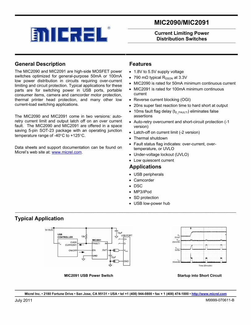
Typical Application
MIC2091 USB Power Switch Startup into Short Circuit
July 2011
M9999-070611-B
Micrel, Inc. MIC2090/MIC2091
July 2011 2 M9999-070611-B
Ordering Information
Part Number Marking Current Limit
Current-Limit Recovery
Junction Temperature Range Package
MIC2090-1YM5 L1K 50mA Auto-Retry –40°C to +125°C SOT-23-5
MIC2091-1YM5 M1K 100mA Auto-Retry –40°C to +125°C SOT-23-5
MIC2090-2YM5 L2K 50mA Latch-Off –40°C to +125°C SOT-23-5
MIC2091-2YM5 M2K 100mA Latch-Off –40°C to +125°C SOT-23-5
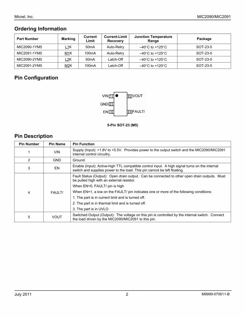
Pin Configuration
5-Pin SOT-23 (M5)
Pin Description Pin Number Pin Name Pin Function
1 VIN Supply (Input): +1.8V to +5.5V. Provides power to the output switch and the MIC2090/MIC2091 internal control circuitry.
2 GND Ground.
3 EN Enable (Input): Active-high TTL compatible control input. A high signal turns on the internal switch and supplies power to the load. This pin cannot be left floating.
4 FAULT/
Fault Status (Output): Open drain output. Can be connected to other open drain outputs. Must be pulled high with an external resistor. When EN=0, FAULT/ pin is high When EN=1, a low on the FAULT/ pin indicates one or more of the following conditions: 1. The part is in current limit and is turned off. 2. The part is in thermal limit and is turned off. 3. The part is in UVLO
5 VOUT Switched Output (Output): The voltage on this pin is controlled by the internal switch. Connect the load driven by the MIC2090/MIC2091 to this pin.
Micrel, Inc. MIC2090/MIC2091
July 2011 3 M9999-070611-B
Absolute Maximum Ratings(1) Supply Voltage (VIN) ..................................... −0.3V to +6.0V Output Voltage (VOUT). ................................. −0.3V to +6.0V FAULT/ Pin Voltage (VFAULT/) ....................... −0.3V to +6.0V FAULT/ Pin Current (I FAULT/) .......................................25mA EN Pin Voltage (VEN)...........................−0.3V to (VIN + 0.3V) Power Dissipation (PD) .............................. Internally Limited Maximum Junction Temperature (TJ)......................... 150°C Storage Temperature (TS).........................−65°C to +150°C Lead Temperature (soldering, 10s)............................ 260°C ESD HBM Rating(3)......................................................... 3kV ESD MM Rating(3).........................................................200V
Operating Ratings(2) Supply Voltage (VIN)..................................... +1.8V to +5.5V Output Voltage (VOUT) .................................. +1.8V to +5.5V EN Pin Voltage (VEN).............................................. 0V to VIN FAULT/ Pin Voltage (VFAULT/) .............................. 0V to 5.5V FAULT/ Pin Current (I FAULT/) .........................................1mA Ambient Temperature (TA) ..........................–40°C to +85°C Junction Temperature (TJ) ........................–40°C to +125°C Package Thermal Resistance SOT23-5 (θJA) ...............................................252.7°C/W
Electrical Characteristics(4) VIN = 5V; TA = 25°C, bold values indicate –40°C ≤ TA ≤ +85°C, unless noted.
Symbol Parameter Condition Min. Typ. Max. Units
Power Input Supply
VIN Input Voltage Range 1.8 5.5 V
Shutdown Current VEN ≤ 0.5V (switch off), VOUT = open 5 10 IVIN
Supply Current VEN ≥ 1.5V (switch on), VOUT = open 70 110 µA
VUVLO Under-Voltage Lockout Threshold VIN rising 1.75 V
VUVLO_HYS Under-Voltage Lockout Threshold Hysteresis 100 mV
Enable Input
Enable Logic Level High(5) VIH (MIN) 1.5 VEN
Enable Logic Level Low(5) VIL (MAX) 0.5 V
IEN Enable Bias Current VEN = 5V 0.1 µA
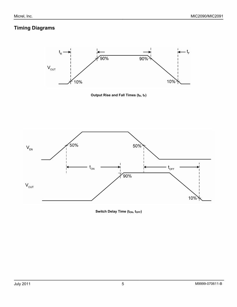
tON Output Turn-On Delay RL = 500Ω, CL = 0.1µF See “Timing Diagrams” 215 µs
tR Output Turn-On Rise Time RL = 500Ω, CL = 0.1µF See “Timing Diagrams” 5 µs
tOFF Output Turn-Off Delay RL = 500Ω, CL = 0.1µF See “Timing Diagrams” 125 µs
tF Output Turn-Off Fall Time RL = 500Ω, CL = 0.1µF See “Timing Diagrams” 115 µs
Internal Switch
MIC2090 VIN = 5.0V, IOUT = 50mA 700 1200
MIC2090 VIN = 3.3V, IOUT = 50mA 790 1200
MIC2090 VIN = 1.8V, IOUT = 50mA 1300
MIC2091 VIN = 5.0V, IOUT = 100mA 700 1200
MIC2091 VIN = 3.3V, IOUT = 100mA 790 1200
RDSON On Resistance RDS(ON)
MIC2091 VIN = 1.8V, IOUT = 100mA 1300
mΩ
Input-to-Output Leakage Current (Forward leakage Current)
MIC2090 and MIC2091, VEN ≤ 0.5V, (output off), VIN = 5.5V, VOUT = 0V 10 μA
Micrel, Inc. MIC2090/MIC2091
July 2011 4 M9999-070611-B
Electrical Characteristics(4) (Continued) VIN = 5V; TA = 25°C, bold values indicate –40°C ≤ TA ≤ +85°C, unless noted.
Symbol Parameter Condition Min. Typ. Max. Units
Output to Input Leakage Current (Reverse Leakage Current)
MIC2090 and MIC2091, VEN ≤ 0.5V, (output off), VOUT = 5.5V, VIN = 0V 10 µA
Current Limit
MIC2090 @ VOUT = 4.5V 50 75 100
MIC2090 @ VOUT = 0V 50 100 150
MIC2091 @ VOUT = 4.5V 100 150 200 ILIMIT Current-Limit Threshold
MIC2091 @ VOUT = 0V 100 175 250
mA
tSC_RESP Short-Circuit Response Time
Short circuit applied to output after switch is turned on, see “Timing Diagrams”. VIN = 3.3V. 20 ns
TAUTORESTART
Time After Switch Shuts Down From An Over-Current Condition Before It Tries To Turn On Again.
30 60 90 ms
FAULT/ Flag
Error Flag Output Voltage Output voltage high (1mA Sinking) 0.4 V
tD_FAULT/
Time After Switch Comes Into Current Limit Before The PIN FAULT/ Is Pulled Low.
When an over-current condition happens, the part will go into constant output current for this time. After this time it will turn off the output and pull low the PIN FAULT/. The MIC2090-1 and MIC2091-1 will automatically restart themselves after the auto restart time TAUTORESTART.
5 10 20 ms
tR_FAULT/ FAULT/ Rising Time FAULT/ is connected to VIN = 5V through 10kΩ and 100pF in parallel. See “Timing Diagrams” 5 µs
tF_FAULT/ FAULT/ Falling Time 1 µs
Reverse Voltage Protection (OGI)
OGI Output Voltage Greater Than Input Voltage (OGI)
If the output voltage is greater than the input voltage by this amount, the part will shut down. The enable pin must be recycled to reset.
85 mV
OGITIME Time that the output voltage can be greater than the input voltage before the chip is shut down.
10 ms
Thermal Protection
TJ Rising 150 TOVERTEMP Over-Temperature
Shutdown TJ Falling 140 °C
Notes: 1. Exceeding the absolute maximum rating may damage the device. 2. The device is not guaranteed to function outside its operating rating. 3. Devices are ESD sensitive. Handling precautions recommended. Human body model, 1.5k in series with 100pF. 4. Specification for packaged product only. 5. VIL(MAX) = Maximum positive voltage applied to the input which will be accepted by the device as a logic low.
VIH(MIN) = Minimum positive voltage applied to the input which will be accepted by the device as a logic high.
Micrel, Inc. MIC2090/MIC2091
July 2011 5 M9999-070611-B
Timing Diagrams
Output Rise and Fall Times (tR, tF)
Switch Delay Time (tON, tOFF)
Micrel, Inc. MIC2090/MIC2091
July 2011 6 M9999-070611-B
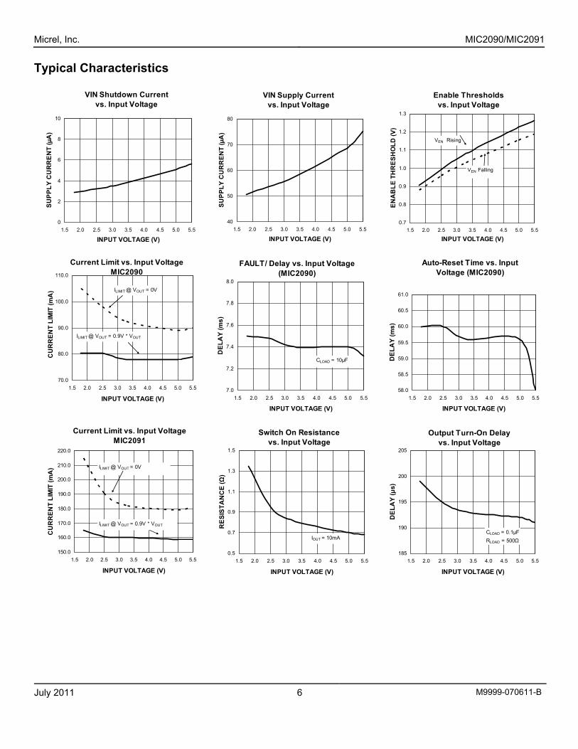
Typical Characteristics
VIN Shutdown Current vs. Input Voltage
0
2
4
6
8
10
1.5 2.0 2.5 3.0 3.5 4.0 4.5 5.0 5.5
INPUT VOLTAGE (V)
SUPP
LY C
UR
REN
T (µ
A)
VIN Supply Current vs. Input Voltage
40
50
60
70
80
1.5 2.0 2.5 3.0 3.5 4.0 4.5 5.0 5.5
INPUT VOLTAGE (V)
SUPP
LY C
UR
REN
T (µ
A)
Enable Thresholdsvs. Input Voltage
0.7
0.8
0.9
1.0
1.1
1.2
1.3
1.5 2.0 2.5 3.0 3.5 4.0 4.5 5.0 5.5
INPUT VOLTAGE (V)
ENA
BLE
TH
RES
HO
LD (V
)
VEN Rising
VEN Falling
Current Limit vs. Input Voltage MIC2090
70.0
80.0
90.0
100.0
110.0
1.5 2.0 2.5 3.0 3.5 4.0 4.5 5.0 5.5
INPUT VOLTAGE (V)
CU
RR
ENT
LIM
IT (m
A)
ILIMIT @ VOUT = 0.9V * VOUT
ILIMIT @ VOUT = 0V
FAULT/ Delay vs. Input Voltage (MIC2090)
7.0
7.2
7.4
7.6
7.8
8.0
1.5 2.0 2.5 3.0 3.5 4.0 4.5 5.0 5.5
INPUT VOLTAGE (V)
DEL
AY
(ms)
CLOAD = 10μF
Auto-Reset Time vs. Input Voltage (MIC2090)
58.0
58.5
59.0
59.5
60.0
60.5
61.0
1.5 2.0 2.5 3.0 3.5 4.0 4.5 5.0 5.5
INPUT VOLTAGE (V)
DEL
AY
(ms)
Current Limit vs. Input Voltage MIC2091
150.0
160.0
170.0
180.0
190.0
200.0
210.0
220.0
1.5 2.0 2.5 3.0 3.5 4.0 4.5 5.0 5.5
INPUT VOLTAGE (V)
CU
RR
ENT
LIM
IT (m
A)
ILIMIT @ VOUT = 0.9V * VOUT
ILIMIT @ VOUT = 0V
Switch On Resistancevs. Input Voltage
0.5
0.7
0.9
1.1
1.3
1.5
1.5 2.0 2.5 3.0 3.5 4.0 4.5 5.0 5.5
INPUT VOLTAGE (V)
RES
ISTA
NC
E (Ω
)
IOUT = 10mA
Output Turn-On Delayvs. Input Voltage
185
190
195
200
205
1.5 2.0 2.5 3.0 3.5 4.0 4.5 5.0 5.5
INPUT VOLTAGE (V)
DEL
AY
(μs)
CLOAD = 0.1μFRLOAD = 500Ω
Micrel, Inc. MIC2090/MIC2091
July 2011 7 M9999-070611-B
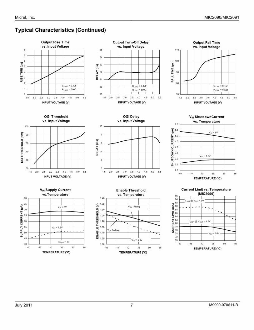
Typical Characteristics (Continued)
Output Rise Timevs. Input Voltage
0
1
2
3
4
5
6
7
8
1.5 2.0 2.5 3.0 3.5 4.0 4.5 5.0 5.5
INPUT VOLTAGE (V)
RIS
E TI
ME
(μs)
CLOAD = 0.1μFRLOAD = 500Ω
Output Turn-Off Delayvs. Input Voltage
29
30
31
32
33
34
35
1.5 2.0 2.5 3.0 3.5 4.0 4.5 5.0 5.5
INPUT VOLTAGE (V)
DEL
AY
(μs)
CLOAD = 0.1μFRLOAD = 500Ω
Output Fall Timevs. Input Voltage
70
80
90
100
110
1.5 2.0 2.5 3.0 3.5 4.0 4.5 5.0 5.5
INPUT VOLTAGE (V)
FALL
TIM
E (μ
s)
CLOAD = 0.1μFRLOAD = 500Ω
OGI Thresholdvs. Input Voltage
50
60
70
80
90
100
1.5 2.0 2.5 3.0 3.5 4.0 4.5 5.0 5.5
INPUT VOLTAGE (V)
OG
I TH
RES
HO
LD (m
V)
OGI Delayvs. Input Voltage
5
6
7
8
9
10
1.5 2.0 2.5 3.0 3.5 4.0 4.5 5.0 5.5
INPUT VOLTAGE (V)
DEL
AY
(ms)
VIN ShutdownCurrent vs. Temperature
2.0
2.5
3.0
3.5
4.0
4.5
5.0
5.5
6.0
-40 -15 10 35 60 85
TEMPERATURE (°C)
SHU
TDO
WN
CU
RR
ENT
(µA
)
VIN = 5V
VIN = 1.8V
VIN Supply Current vs.Temperature
40
45
50
55
60
65
70
75
80
-40 -15 10 35 60 85
TEMPERATURE (°C)
SUPP
LY C
UR
REN
T (µ
A)
VIN = 5V
VIN = 1.8V
RLOAD = 0
Enable Threshold vs. Temperature
1.00
1.05
1.10
1.15
1.20
1.25
1.30
1.35
1.40
-40 -15 10 35 60 85
TEMPERATURE (°C)
ENA
BLE
TH
RES
HO
LD (V
)
VEN Rising
VEN Falling
VIN = 5.0V
Current Limit vs. Temperature (MIC2090)
7072747678808284868890929496
-40 -15 10 35 60 85
TEMPERATURE (°C)
CU
RR
ENT
LIM
IT (m
A)
VIN = 5.0V
ILIMIT @ VOUT = 0V
ILIMIT @ VOUT = 4.5V
Micrel, Inc. MIC2090/MIC2091
July 2011 8 M9999-070611-B
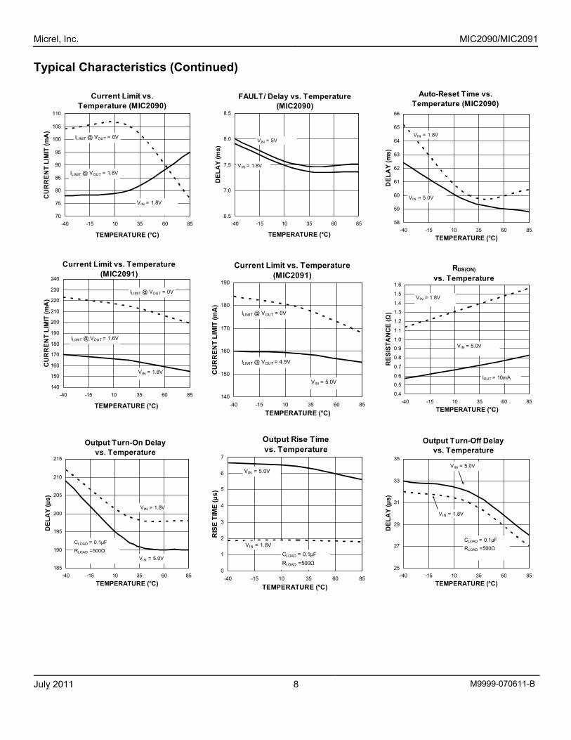
Typical Characteristics (Continued)
Current Limit vs.Temperature (MIC2090)
70
75
80
85
90
95
100
105
110
-40 -15 10 35 60 85
TEMPERATURE (°C)
CU
RR
EN
T LI
MIT
(mA
)
VIN = 1.8V
ILIMIT @ VOUT = 0V
ILIMIT @ VOUT = 1.6V
FAULT/ Delay vs. Temperature (MIC2090)
6.5
7.0
7.5
8.0
8.5
-40 -15 10 35 60 85
TEMPERATURE (°C)
DEL
AY
(ms)
VIN = 5V
VIN = 1.8V
Auto-Reset Time vs. Temperature (MIC2090)
58
59
60
61
62
63
64
65
66
-40 -15 10 35 60 85TEMPERATURE (°C)
DEL
AY
(ms)
VIN = 1.8V
VIN = 5.0V
Current Limit vs. Temperature (MIC2091)
140
150
160
170
180
190
200
210
220
230
240
-40 -15 10 35 60 85
TEMPERATURE (°C)
CU
RR
EN
T LI
MIT
(mA
)
VIN = 1.8V
ILIMIT @ VOUT = 0V
ILIMIT @ VOUT = 1.6V
Current Limit vs. Temperature (MIC2091)
140
150
160
170
180
190
-40 -15 10 35 60 85TEMPERATURE (°C)
CU
RR
ENT
LIM
IT (m
A)
VIN = 5.0V
ILIMIT @ VOUT = 0V
ILIMIT @ VOUT = 4.5V
RDS(ON)
vs. Temperature
0.4
0.5
0.6
0.7
0.8
0.9
1.0
1.1
1.2
1.3
1.4
1.5
1.6
-40 -15 10 35 60 85TEMPERATURE (°C)
RES
ISTA
NC
E (Ω
)
VIN = 5.0V
VIN = 1.8V
IOUT = 10mA
Output Turn-On Delayvs. Temperature
185
190
195
200
205
210
215
-40 -15 10 35 60 85TEMPERATURE (°C)
DEL
AY
(μs)
VIN = 1.8V
VIN = 5.0V
CLOAD = 0.1μFRLOAD =500Ω
Output Rise Timevs. Temperature
0
1
2
3
4
5
6
7
-40 -15 10 35 60 85TEMPERATURE (°C)
RIS
E T
IME
(μs)
VIN = 1.8V
VIN = 5.0V
CLOAD = 0.1μFRLOAD =500Ω
Output Turn-Off Delayvs. Temperature
25
27
29
31
33
35
-40 -15 10 35 60 85TEMPERATURE (°C)
DEL
AY
(μs)
VIN = 1.8V
VIN = 5.0V
CLOAD = 0.1μFRLOAD =500Ω
Micrel, Inc. MIC2090/MIC2091
July 2011 9 M9999-070611-B
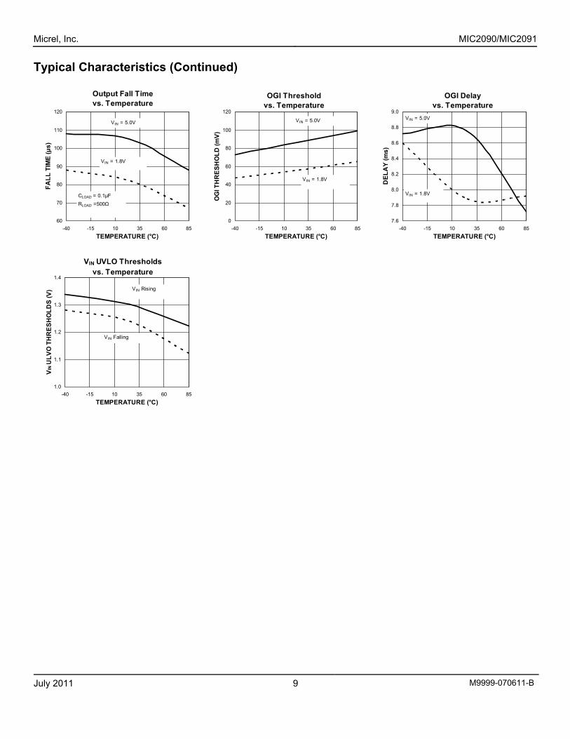
Typical Characteristics (Continued)
Output Fall Timevs. Temperature
60
70
80
90
100
110
120
-40 -15 10 35 60 85TEMPERATURE (°C)
FALL
TIM
E (μ
s)
VIN = 1.8V
VIN = 5.0V
CLOAD = 0.1μFRLOAD =500Ω
OGI Thresholdvs. Temperature
0
20
40
60
80
100
120
-40 -15 10 35 60 85TEMPERATURE (°C)
OG
I TH
RES
HO
LD (m
V)
VIN = 1.8V
VIN = 5.0V
OGI Delayvs. Temperature
7.6
7.8
8.0
8.2
8.4
8.6
8.8
9.0
-40 -15 10 35 60 85TEMPERATURE (°C)
DEL
AY
(ms)
VIN = 1.8V
VIN = 5.0V
VIN UVLO Thresholdsvs. Temperature
1.0
1.1
1.2
1.3
1.4
-40 -15 10 35 60 85TEMPERATURE (°C)
VIN U
LVO
TH
RES
HO
LDS
(V) VIN Rising
VIN Falling
Micrel, Inc. MIC2090/MIC2091
July 2011 10 M9999-070611-B
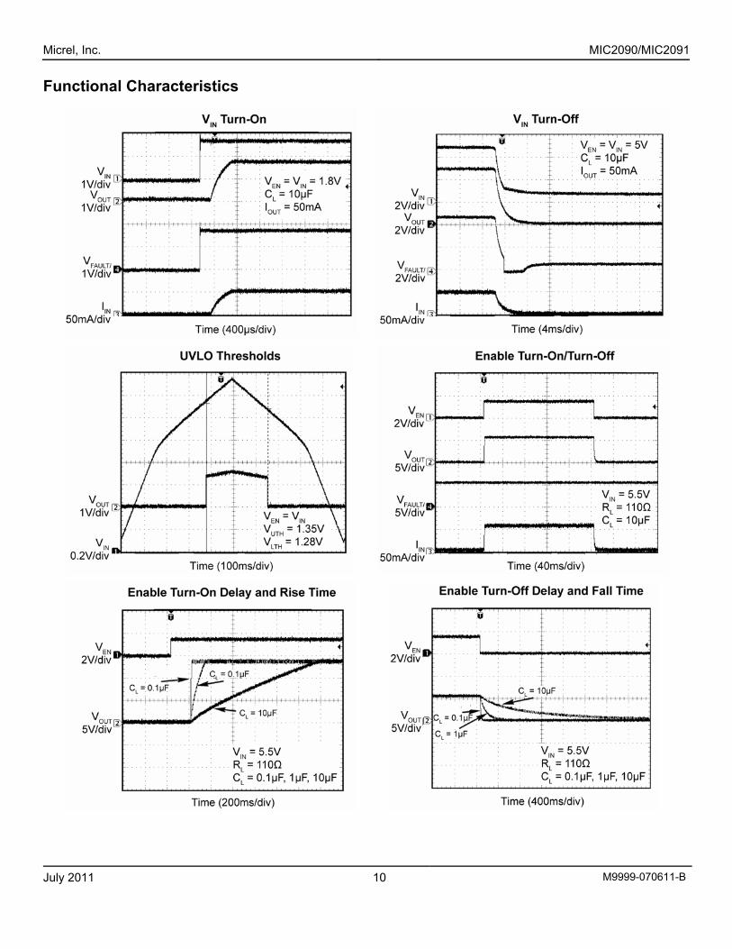
Functional Characteristics
Micrel, Inc. MIC2090/MIC2091
July 2011 11 M9999-070611-B
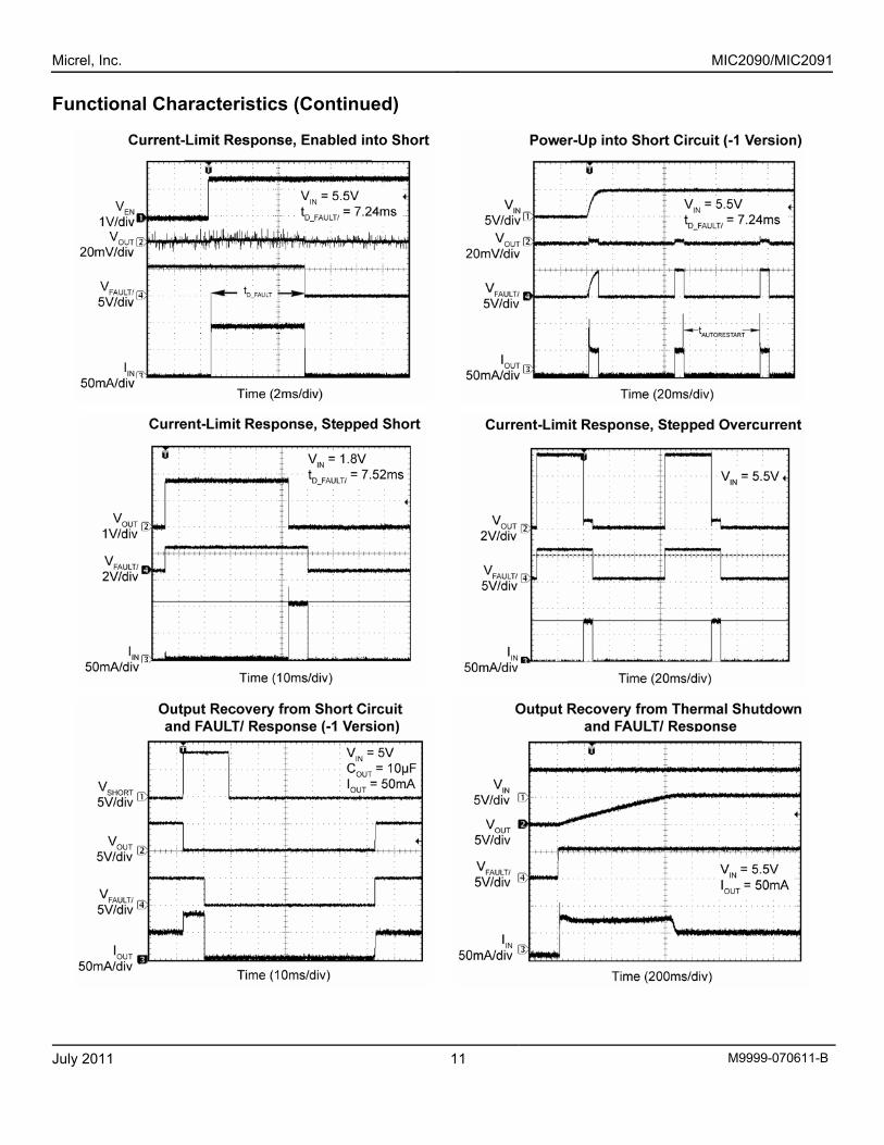
Functional Characteristics (Continued)
Micrel, Inc. MIC2090/MIC2091
July 2011 12 M9999-070611-B
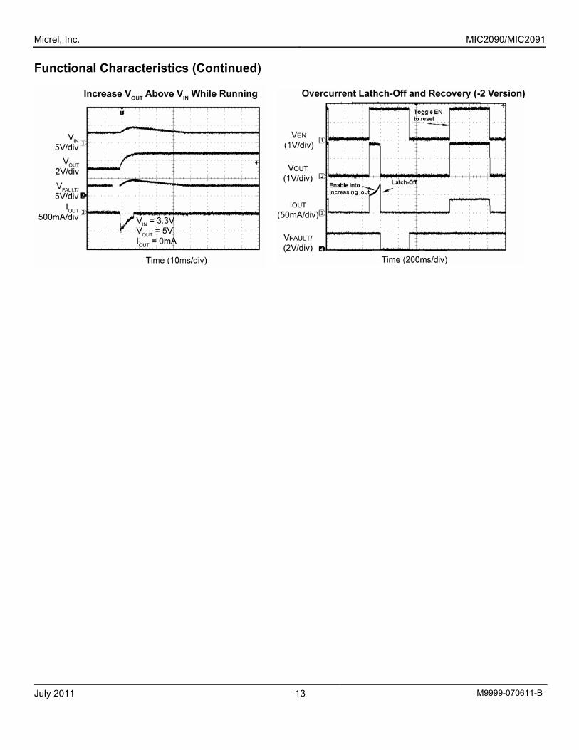
Functional Characteristics (Continued)
Micrel, Inc. MIC2090/MIC2091
July 2011 13 M9999-070611-B
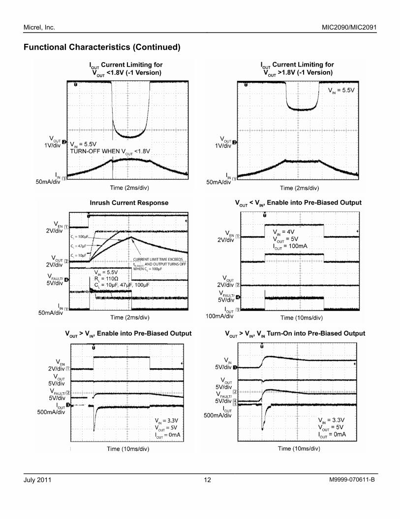
Functional Characteristics (Continued)
Micrel, Inc. MIC2090/MIC2091
July 2011 14 M9999-070611-B
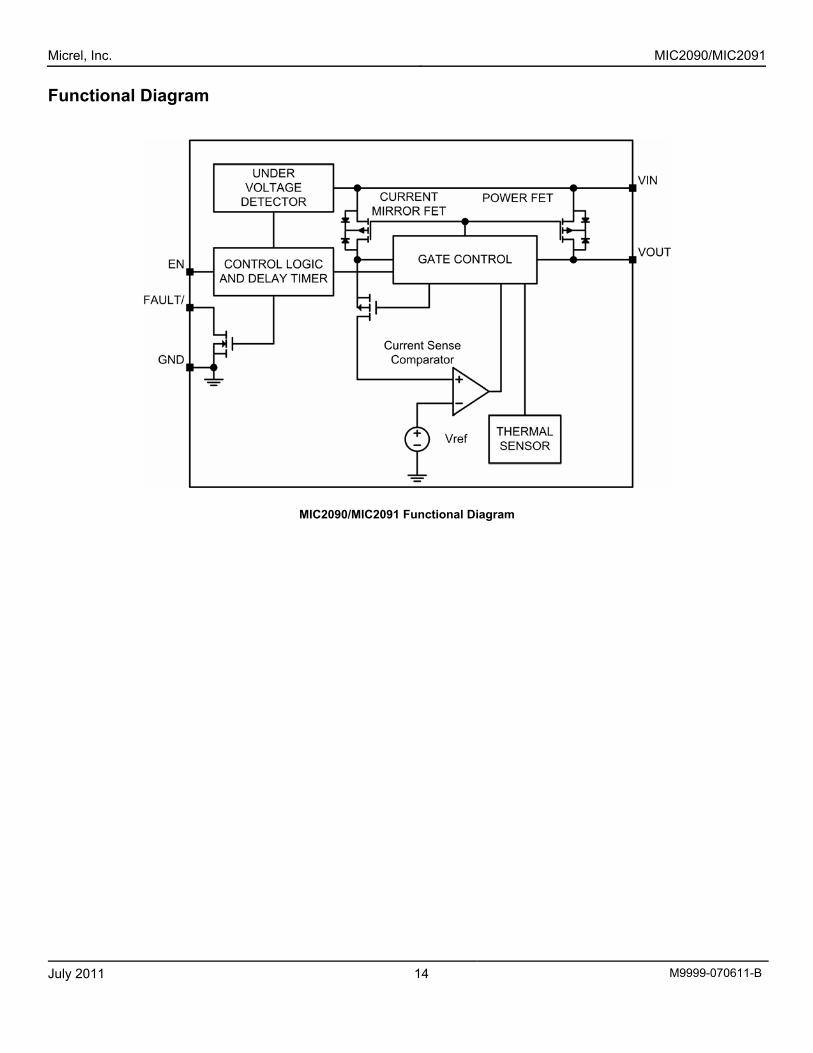
Functional Diagram
MIC2090/MIC2091 Functional Diagram
Micrel, Inc. MIC2090/MIC2091
July 2011 15 M9999-070611-B
Functional Description
VIN and VOUT VIN is both the power supply connection for the internal circuitry driving the switch and the input (source connection) of the power MOSFET switch. VOUT is the drain connection of the power MOSFET and supplies power to the load. In a typical circuit, current flows from VIN to VOUT toward the load. When the switch is disabled, current will not flow to the load, except for a small unavoidable leakage current of a few microamps (forward leakage current).
CIN
A minimum 1μF bypass capacitor positioned close to the VIN and GND pins of the switch is both good design practice and required for proper operation of the switch. This will control supply transients and ringing. Without a sufficient bypass capacitor, large current surges or a short may cause sufficient ringing on VIN (from supply lead inductance) to cause erratic operation of the switch’s control circuitry. For best performance, place a ceramic capacitor next to the IC. An additional 10µF (or greater) capacitor, positioned close to the VIN and GND pins of the switch is necessary if the distance between a larger bulk capacitor and the switch is greater than three inches. This additional capacitor limits input voltage transients at the switch caused by fast changing input currents that occur during a fault condition, such as current limit and thermal shutdown. When bypassing with capacitors of 10μF or more, it is good practice to place a smaller value capacitor in parallel with the larger to handle the high-frequency components of any line transients. Values in the range of 0.1μF to 1μF are recommended. Again, good quality, low-ESR capacitors, preferably ceramic, should be chosen.
COUT An output capacitor is required to reduce ringing and voltage sag on the output during a transient condition. A value between 1μF and 10μF is recommended. A 10μF or larger capacitor should be used if the distance between the MIC2090/MIC2091 and the load is greater than three inches. The internal switch in the MIC2090/MIC2091 turns off in (typically) 20ns. This extremely fast turn-off can cause an inductive spike in the output voltage when the internal switch turns off during an overcurrent condition. The larger value capacitor prevents the output from glitching too low.
Limitations on COUT
The part may enter current limit when turning on with a large output capacitance, which is an acceptable condition. However, if the part remains in current limit for a time greater than tD_FAULT, the FAULT/ pin will assert low. The maximum value of COUT may be approximated by Equation 1:
IN_MAX
ND_FAULT_MILIMIT_MINOUT_MAX V
TIC
×= Eq. 1
Where: ILIMIT_MIN and TD_FAULT_MIN are the minimum specified values listed in the Electrical Characteristic table and VIN_MAX is the maximum input voltage to the switch.
Current Sensing and Limiting The MIC2090/MIC2091 protects the system power supply and load from damage by continuously monitoring current through the on-chip power MOSFET. Load current is monitored by means of a current mirror in parallel with the power MOSFET switch. Current limiting is invoked when the load exceeds the over-current threshold. When current limiting is activated in the -1 version, the output current is constrained to the limit value, and remains at this level until either the load/fault is removed, the load’s current requirement drops below the limiting value, or the switch goes into thermal shutdown. If the overcurrent fault is large enough to drop VOUT below (typically) 1.8V, the internal MOSFET turns off very quickly (typically 20ns). This prevents excessive current from flowing through the device and damaging the internal MOSFET. The latch-off feature of the -2 version latches the output off when the output current exceeds the overcurrent threshold. VIN or the enable pin must be toggled to reset the latch.
Enable Input The EN pin is a TTL logic level compatible input which turns the internal MOSFET switch on and off. The FAULT/ pin remains high when the EN pin is pulled low and the output is turned off. Toggling the enable pin resets the output after an OGI (output greater than input) condition occurs. In the -2 version, toggling the enable pin resets the output after an overcurrent event.
Fault Output The FAULT/ is an N-channel open-drain output, which is asserted LOW when the MIC2090/MIC2091 switch either begins current limiting or enters thermal shutdown.
Micrel, Inc. MIC2090/MIC2091
July 2011 16 M9999-070611-B
During an overcurrent or short circuit, The FAULT/ signal asserts after a brief delay period, tD_FAULT/, in order to filter out false or transient over-current conditions. The FAULT/ output is open-drain and must be pulled HIGH with an external resistor. The FAULT/ signal may be wire-OR’d with other similar outputs, sharing a single pull-up resistor.
Power Dissipation and Thermal Shutdown Thermal shutdown is used to protect the MIC2090/MIC2091 switch from damage should the die temperature exceed a safe operating temperature. Thermal shutdown shuts off the output MOSFET and asserts the FAULT/ output if the die temperature reaches the over-temperature threshold, TOVERTEMP. The switch will automatically resume operation when the die temperature cools down to 140°C. If resumed operation results in reheating of the die, another shutdown cycle will occur and the switch will continue cycling between ON and OFF states until the reason for the overcurrent condition has been resolved. Depending upon the PCB layout, package type, ambient temperature, etc., hundreds of milliseconds may elapse from the time a fault occurs to the time the output MOSFET will be shut off. This delay is caused because of the time it takes for the die to heat after the fault condition occurs. Power dissipation depends on several factors such as the load, PCB layout, ambient temperature, and supply voltage. Calculation of power dissipation can be accomplished by Equation 2:
PD = RDS(ON) × (IOUT)2 Eq.2 To relate this to junction temperature, Equation 3 can be used:
TJ = PD × Rθ(J-A) + TA Eq. 3 Where:
TJ = Junction Temperature TA = Ambient Temperature
Rθ(J-A) is the thermal resistance of the package. In normal operation, excessive switch heating is most often caused by an output short circuit. If the output is shorted, when the switch is enabled, the MIC2090/MIC2091 switch limits the output current to the maximum value. The heat generated by the power dissipation of the switch continuously limiting the current
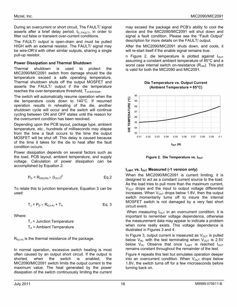
may exceed the package and PCB’s ability to cool the device and the MIC2090/MIC2091 will shut down and signal a fault condition. Please see the “Fault Output” description for more details on the FAULT/ output. After the MIC2090/MIC2091 shuts down, and cools, it will re-start itself if the enable signal remains true. n Figure 2, die temperature is plotted against IOUT assuming a constant ambient temperature of 85°C and a worst case internal switch on-resistance (RON). This plot is valid for both the MIC2090 and MIC2091.
Die Temperature vs. Output Current (Ambient Temperature = 85°C)
83
84
85
86
87
88
89
90
0.01 0.02 0.03 0.04 0.05 0.06 0.07 0.08 0.09 0.1
IOUT (A)
DIE
TEM
PER
ATU
RE
(°C)
Figure 2. Die Temperature vs. IOUT
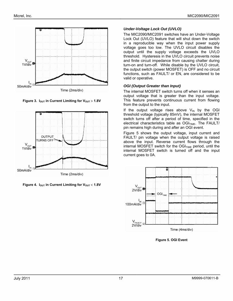
ILIMIT vs. IOUT Measured (-1 version only) When the MIC2090/MIC2091 is current limiting, it is designed to act as a constant current source to the load. As the load tries to pull more than the maximum current, VOUT drops and the input to output voltage differential increases. When VOUT drops below 1.8V, then the output switch momentarily turns off to insure the internal MOSFET switch is not damaged by a very fast short circuit event. When measuring IOUT in an overcurrent condition, it is important to remember voltage dependence, otherwise the measurement data may appear to indicate a problem when none really exists. This voltage dependence is illustrated in Figures 3 and 4. In Figure 3, output current is measured as VOUT is pulled below VIN, with the test terminating when VOUT is 2.5V below VIN. Observe that once ILIMIT is reached IOUT remains constant throughout the remainder of the test. Figure 4 repeats this test but simulates operation deeper into an overcurrent condition. When VOUT drops below 1.8V, the switch turns off for a few microseconds before turning back on.
Micrel, Inc. MIC2090/MIC2091
July 2011 17 M9999-070611-B
Figure 3. IOUT in Current Limiting for VOUT > 1.8V
Figure 4. IOUT in Current Limiting for VOUT < 1.8V
Under-Voltage Lock Out (UVLO) The MIC2090/MIC2091 switches have an Under-Voltage Lock Out (UVLO) feature that will shut down the switch in a reproducible way when the input power supply voltage goes too low. The UVLO circuit disables the output until the supply voltage exceeds the UVLO threshold. Hysteresis in the UVLO circuit prevents noise and finite circuit impedance from causing chatter during turn-on and turn-off. While disable by the UVLO circuit, the output switch (power MOSFET) is OFF and no circuit functions, such as FAULT/ or EN, are considered to be valid or operative.
OGI (Output Greater than Input) The internal MOSFET switch turns off when it senses an output voltage that is greater than the input voltage. This feature prevents continuous current from flowing from the output to the input. If the output voltage rises above VIN by the OGI threshold voltage (typically 85mV), the internal MOSFET switch turns off after a period of time, specified in the electrical characteristics table as OGITIME. The FAULT/ pin remains high during and after an OGI event. Figure 5 shows the output voltage, input current and FAULT/ pin voltage when the output voltage is raised above the input. Reverse current flows through the internal MOSFET switch for the OGITIME period, until the internal MOSFET switch is turned off and the input current goes to 0A.
Figure 5. OGI Event
Micrel, Inc. MIC2090/MIC2091
July 2011 18 M9999-070611-B
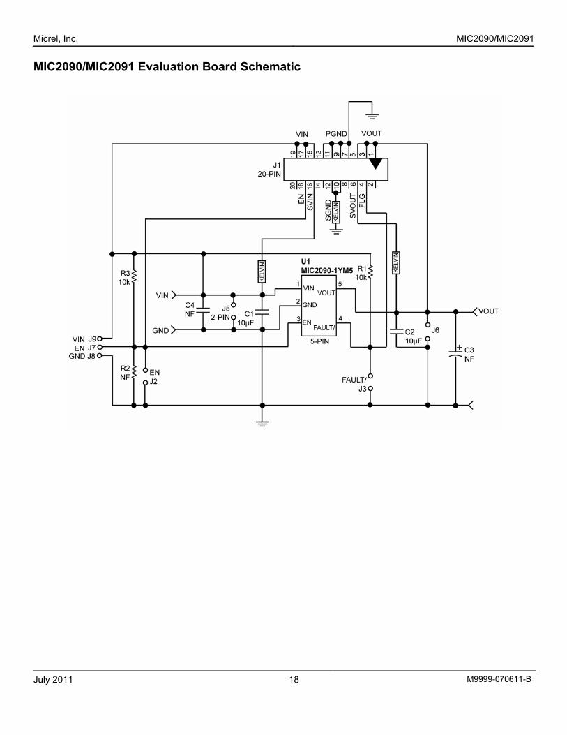
MIC2090/MIC2091 Evaluation Board Schematic
Micrel, Inc. MIC2090/MIC2091
July 2011 19 M9999-070611-B
Bill of Materials Item Part Number Manufacturer Description Qty. C1, C2 08056D106MAT2A AVX(1) 10µF, 6.3V Ceramic Capacitor, X5R 2 C3, C4 NF (No Fill) 2 R1, R3 CRCW06031002FRT1 Vishay Dale(2) 10k, 1%, 0603 Resistor 2 R2 NF (No Fill) 1 U1 MIC2090-1YM5 Micrel, Inc.(3) Current Limiting Power Distribution Switch 1 U1 MIC2091-1YM5 Micrel, Inc.(3) Current Limiting Power Distribution Switch 0 U1 MIC2090-2YM5 Micrel, Inc.(3) Current Limiting Power Distribution Switch 0 U1 MIC2091-2YM5 Micrel, Inc.(3) Current Limiting Power Distribution Switch 0
Notes: 1. AVX: www.avx.com. 2. Vishay Tel: www.vishay.com. 3. Micrel, Inc.: www.micrel.com.
Micrel, Inc. MIC2090/MIC2091
July 2011 20 M9999-070611-B
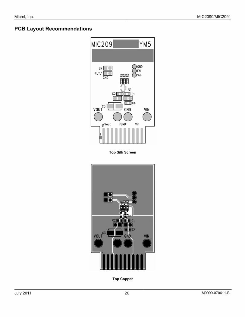
PCB Layout Recommendations
Top Silk Screen
Top Copper
Micrel, Inc. MIC2090/MIC2091
July 2011 21 M9999-070611-B
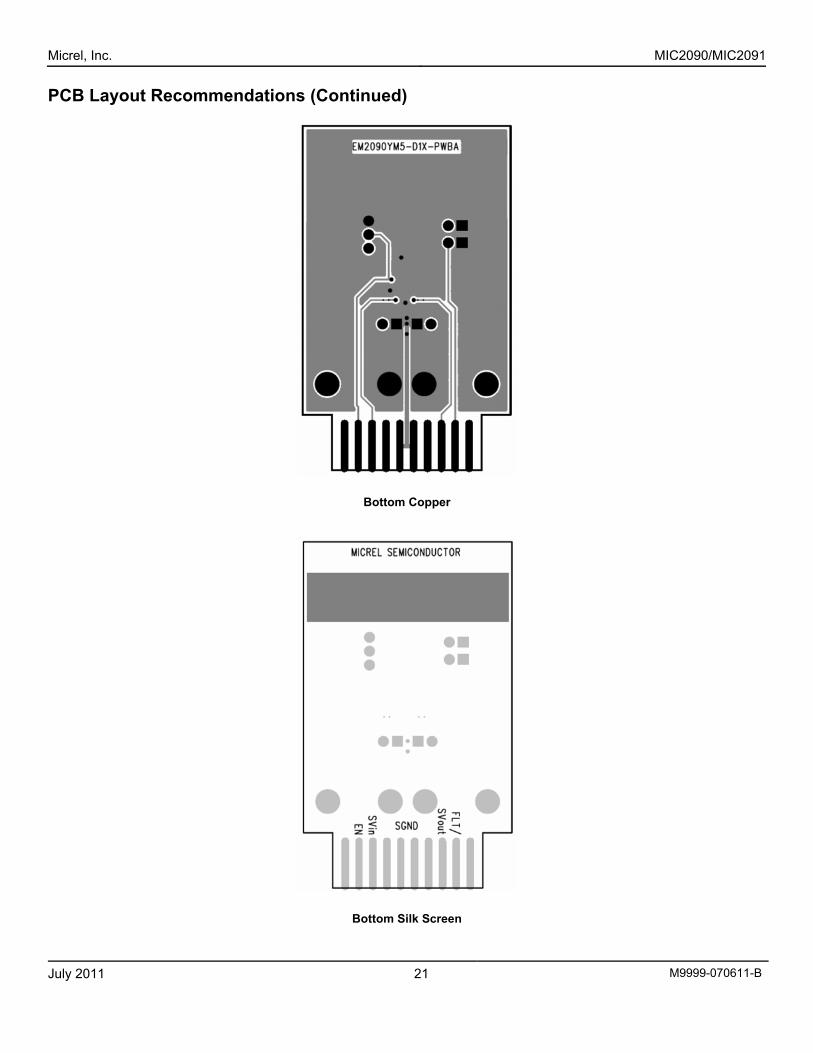
PCB Layout Recommendations (Continued)
Bottom Copper
Bottom Silk Screen
Micrel, Inc. MIC2090/MIC2091
July 2011 22 M9999-070611-B
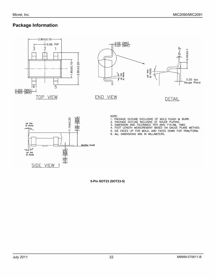
Package Information
5-Pin SOT23 (SOT23-5)
Micrel, Inc. MIC2090/MIC2091
July 2011 23 M9999-070611-B
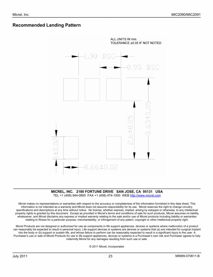
Recommended Landing Pattern
MICREL, INC. 2180 FORTUNE DRIVE SAN JOSE, CA 95131 USA TEL +1 (408) 944-0800 FAX +1 (408) 474-1000 WEB http://www.micrel.com
Micrel makes no representations or warranties with respect to the accuracy or completeness of the information furnished in this data sheet. This
information is not intended as a warranty and Micrel does not assume responsibility for its use. Micrel reserves the right to change circuitry, specifications and descriptions at any time without notice. No license, whether express, implied, arising by estoppel or otherwise, to any intellectual
property rights is granted by this document. Except as provided in Micrel’s terms and conditions of sale for such products, Micrel assumes no liability whatsoever, and Micrel disclaims any express or implied warranty relating to the sale and/or use of Micrel products including liability or warranties
relating to fitness for a particular purpose, merchantability, or infringement of any patent, copyright or other intellectual property right.
Micrel Products are not designed or authorized for use as components in life support appliances, devices or systems where malfunction of a product reasonably be expected to result in personal injury. Life support devices or systems are devices or systems that (a) are intended for surgical implainto the body or (b) support or sustain life, and whose failure to perform can be reasonably expected to result in a significant injury to the user. A
Purchaser’s use or sale of Micrel Products for use in life support appliances, devices or systems is a Purchaser’s own risk and Purchaser agrees to fully indemnify Micrel for any damages resulting from such use or sale.
can nt
© 2011 Micrel, Incorporated.