Embed Size (px)
Citation preview
Mercaptophosphonic acids as efficient linkers in quantum
dot sensitized solar cells
Journal: Journal of Materials Chemistry A
Manuscript ID: TA-ART-06-2015-004021.R1
Article Type: Paper
Date Submitted by the Author: 31-Jul-2015
Complete List of Authors: Aldakov, Dmitry; CEA-Grenoble, INAC/SPrAM Sajjad, Muhammad; University of St Andrews, SUPA School of Physics and Astronomy Ivanova, Valentina; CEA-Leti, Bansal, Ashu; University of St Andrews, SUPA School of Physics and Astronomy
Park, Jinhyung; CEA-Grenoble, INAC/SPrAM Reiss, P; Departement de Recherche Fondamentale sur la Matiere Condensee, CEA Grenoble Samuel, Ifor; St Andrews, Organic Semiconductor Centre
Journal of Materials Chemistry A
1
Mercaptophosphonic acids as efficient linkers in
quantum dot sensitized solar cells
Dmitry Aldakov*,a,b,c
Muhammad T. Sajjad,d Valentina Ivanova,
e Ashu K. Bansal,
d Jinhyung
Park, a,b,c
Peter Reiss, a,b,c
Ifor D. W. Samueld
a Univ. Grenoble Alpes, INAC-SPRAM, F-38000 Grenoble, France
b CNRS, INAC-SPRAM, F-38000 Grenoble, France
c CEA, INAC-SPRAM, F-38000 Grenoble, France
d Organic Semiconductor Centre, School of Physics and Astronomy, University of St Andrews,
North Haugh, St Andrews, Fife, UK
e CEA, LETI, MINATEC Campus, 17 rue des Martyrs, 38054 Grenoble, France
KEYWORDS. Quantum dots, nanocrystals, quantum dot sensitized solar cells, phosphonic acids,
ZnO nanowires, charge transfer.
Abstract. Control over the deposition of quantum dots (QDs) on nanostructured semiconductors
is very important for the photovoltaic performance of QD sensitized solar cells. The best control
is typically achieved using bifunctional molecular linkers, such as mercaptopropionic acid
(MPA), to attach the QDs to metal oxides in a specific manner; however some materials, such as
ZnO, are not compatible with these molecules due to their pH sensitivity. We have developed
Page 1 of 35 Journal of Materials Chemistry A
2
new linkers, mercaptophosphonic acids of different length, which allow for efficient
functionalization of ZnO nanowires and also mesoporous TiO2 without damaging their surface.
Detailed XPS and contact angle studies of the mechanism of self-assembly of these acids show
that their strong chelation of the oxide surface prevents from protonic attack and etching. Using
these linkers, we show that colloidal ternary quantum dots, CuInS2, can be conformally and
homogeneously deposited on the functionalized metal oxides. Photophysical studies by means of
time-resolved photoluminescence spectroscopy confirm efficient electron transfer from the QDs
to the metal oxides with the rate and efficiency scaling with respect to the linker length and
nature. The efficiency of the QD sensitized solar cells fabricated with such assemblies also
strongly depends on the linkers used and follows the trends observed for the charge transfer.
Introduction
Quantum dots (QDs) have a series of appealing properties such as high absorption coefficients,
size dependence and easy tunability of their optical and electronic properties due to quantum
confinement, which make them very attractive materials for applications in different
technological areas, including biological labelling, light-emitting diodes and photovoltaic
devices. Furthermore, semiconductor QDs offer the possibility of multiple exciton generation,1
which could allow them to overcome the Shockley−Queisser limit in solar cells.2 QD based solar
cells are widely considered as a photovoltaic technology providing a high potential for becoming
a viable alternative to silicon and inorganic thin film based cells, and were recently called “the
next big thing in photovoltaics”.3
QD sensitized solar cells (QDSSCs) inherit the configuration of dye sensitized cells and their
efficiencies are rapidly progressing with a recent record of 8.21%.4 It is of high importance for
photovoltaic applications to have controlled surface properties and size distribution of the QDs to
Page 2 of 35Journal of Materials Chemistry A
3
avoid charge recombination and trapping. Colloidal QDs allow for tailored surface engineering
and narrow size distribution, in addition they have the advantage of reproducible synthesis,
which can be separated from the solar cell fabrication process. Moreover, specific organic
ligands or inorganic external shells can be used to passivate their surface in order to avoid charge
carrier trapping. Thus, the preparation of QDs can be improved independently before supplying
QD inks with optimal properties ready for deposition in the cell. Currently, most of the colloidal
QDs used for solar cells contain toxic metals such as Pb and Cd, which limit the upscaling and
further industrial uptake. Development of “eco-friendly” QDs without heavy elements is thus of
high importance. Ternary and quaternary nanocrystals combine the classical advantages of QDs
with their non-toxicity and possibility to fine tune their properties in a larger range due to the
wider choice of composition.5 Recently, several important works showing a successful use of
non-toxic ternary colloidal QDs in QDSSCs have appeared;6–14 typically the QDs are deposited
on TiO2 with only one example of sensitization of ZnO nanowires.15
There are several ways to deposit colloidal QDs onto nanostructured metal oxides (NMOs):
simple physisorption, electrophoresis, or linker-assisted deposition (self-assembly). The last of
these possibilities is typically considered as resulting in the best control over the QD coverage,
moreover it allows to fine tune the distance between the QDs and a NMO in order to maximise
charge transfer and minimise recombination processes.16–18 The nature of the linker molecule
plays an important role in the charge transfer process: its anchoring group can have an effect on
the charge injection;19–22 its conjugation can facilitate the charge transfer by improving electronic
coupling through a conjugated bridge;23,24 finally, it was shown that the length of the linkers
directly influences the charge transfer dynamics and efficiency.22,24–27 It is generally expected
that the shortest linker binding QDs to NMOs results in better electron injection as the distance
Page 3 of 35 Journal of Materials Chemistry A
4
necessary for electron tunnelling is smaller. However, the linker length dependence is more
complicated as although the charge transfer becomes more efficient for short linkers, the
probability of charge recombination also increases.28 Hence there is trade-off in which the
positive effect of short linkers can be counterbalanced by undesired recombination processes. In
addition, colloidal QDs are typically surrounded by a layer of passivating ligands containing long
alkyl chains, rendering their binding to NMOs via short linkers less efficient.
Linker-assisted deposition using bifunctional molecules can be realized either (i) by
exchanging the ligands on the QDs first with these molecules followed by the attachment of the
QDs to the untreated electrode (ex situ approach); or (ii) by functionalising the NMO first
followed by the assembly of the QDs (in situ approach).16 The ex situ method generally yields
high coverage of the electrodes (reported up to 34%),29,30 however during the ligand exchange
with smaller bifunctional molecules the surface of the QDs can be severely perturbed with the
formation of less passivated spots and occurrence of the defect states. The in situ method is
simpler and even though it generally results in lower QD coverage (around 20%),31–33 it has the
advantage of keeping the pristine passivating ligand shell of the QDs intact and thus naturally
better protects the QD surface against the formation of defects and traps.34 In both the in situ and
ex situ deposition methods, the nature of the NMO has to be taken into account. ZnO, for
example, is easily etched by carboxylic acid type linkers such as widely used 2-
mercaptopropionic acid (MPA).35–39 One of the potential alternatives for the sensitisation of zinc
oxide with QDs is the use of mercaptophosphonic acids. They are known to bind strongly to the
surface of metal oxides due to bi- or tridentate coordination,40–43 and thus the condensation of the
phosphonic acid moiety with the ZnO surface is more stable than that of the carboxylic acid.44
Finally, it has been shown that the charge injection from excited organic dyes to semiconductor
Page 4 of 35Journal of Materials Chemistry A
5
electrodes can be faster when they are adsorbed via phosphonic acid anchors than via carboxylic
acid anchors45,46 even though depending on the dye structure this order can be reversed.47–49 To
the best of our knowledge, no examples of using mercaptophosphonic acids for the attachment of
QDs on NMOs were reported, although one work describes the use of a mercaptophosphinic acid
(R2-PO2H) for the attachment of PbS to TiO2 for QD mesoscopic cells.50 Having the pka and
structure similar to phosphonic acids, phosphinic acids can also be applicable as linkers for
QDSSCs. At the same time, owing to the bidentate binding mode to the NMOs because of the
presence of two substituents, their adsorption constants should be lower compared to phosphonic
acids (having bi- or tridentate coordination), making these latter more promising candidates for
the attachment of QDs to sensitive NMOs, such as ZnO.
The aim of this work is to develop new linkers for the in situ deposition of QDs onto TiO2 and
ZnO nanostructured electrodes in view of their application in solar cells. We show that the use of
mercaptophosphonic acids, so far unexplored as linkers in QD sensitized solar cells, leads to
efficient coverage of the surface of the NMOs enabling the attachment of QDs with various
surface ligands. Moreover, due to the rapid bi- or tridentate binding of the phosphonic acids to
the surface of the NMO, it is compatible even with pH-sensitive ZnO nanowire electrodes. We
have investigated the deposition of the linkers on various substrates by measuring contact angles
and by carrying out a detailed X-ray photoelectron spectroscopy (XPS) analysis to confirm
efficient functionalization and to elucidate the binding mode. Our study shows that the linker
nature and length strongly influence the rate and efficiency of the charge transfer between the
QDs and the semiconductor electrodes. Finally, QD sensitized solar cells based on these
assemblies have been fabricated and characterized. The photovoltaic efficiency of the cells
Page 5 of 35 Journal of Materials Chemistry A
6
strongly depends on the used linker molecule and follows the trends identified by the
photophysical studies.
Results and discussion
Surface functionalization of ZnO and TiO2. Mesoporous TiO2 and ZnO nanowires were first
functionalized with MPA, which has been reported by various groups for the specific deposition
of QDs.17,20,51 Under standard conditions without pH control, the zinc oxide surface was
seriously corroded at the very initial functionalization stages followed by the complete
dissolution of the nanowires at prolonged times. Similar behaviour was observed before in the
case of exposure of ZnO nanostructures to acidic conditions during dye loading and was
explained by the adsorption of protons present in solution followed by the dissolution of the ZnO
material.36,37,39,52 It was estimated that the dissolution of ZnO colloids starts when the pH is
below 7.4.53 In the case of nanowires, the dissolution is face-sensitive and more rapid than in
case of bulk flat films.37
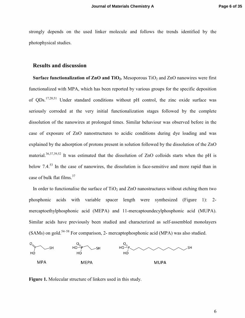
In order to functionalise the surface of TiO2 and ZnO nanostructures without etching them two
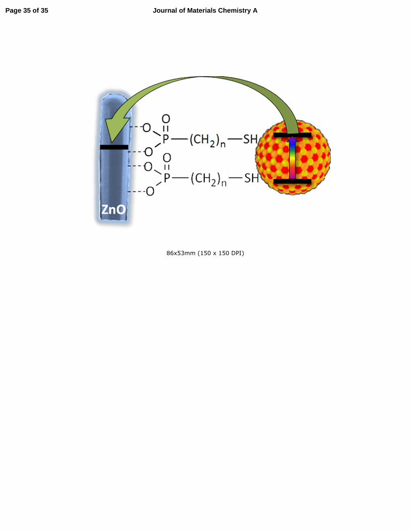
phosphonic acids with variable spacer length were synthesized (Figure 1): 2-
mercaptoethylphosphonic acid (MEPA) and 11-mercaptoundecylphosphonic acid (MUPA).
Similar acids have previously been studied and characterized as self-assembled monolayers
(SAMs) on gold.54–58 For comparison, 2- mercaptophosphonic acid (MPA) was also studied.
Figure 1. Molecular structure of linkers used in this study.
Page 6 of 35Journal of Materials Chemistry A
7
After the functionalization of the ZnO nanowires in the solutions of phosphonic acids, no signs
of surface damage or etching were observed. Alkylphosphonic acids are stronger compared to
alkylcarboxylic acids, with reported values of the first pKa of MUPA SAMs on gold of 2-4.559,60
while that of MPA is 5.5-6.5.61 So one could expect even stronger ZnO etching by phosphonic
acids, which was indeed observed in case of prolonged exposure of a layer of ZnO to different
phosphonic acids.62,63 However, in case of the acids studied in this work other factors likely play
a determining role. Our interpretation of the observed unexpected stability of ZnO nanostructures
in the presence of bifunctional phosphonic acids is as follows: carboxylic acids bind to ZnO in a
mono- or sometimes bidentate mode allowing for reversible adsorption-desorption and exposing
the substrate surface to the protons of the low pH solution, which gradually dissolve ZnO. In the
case of phosphonic acids, the binding is faster and stronger as bi- and tri-dentate surface
coordination modes are preferentially realised,40,41,64 limiting the desorption of bound
phosphonates, which naturally protect the ZnO surface from protonic attack. A similar
phenomenon of protection of flat ZnO surfaces against acidic etching by phosphonic acid SAMs’
has been previously observed by Perkins et al.41
Mercaptophosphonic acids are in principle capable of binding to the ZnO by either the
phosphonate or the thiol group. In the latter case the consequent binding to the QDs will not be
efficient so the exact binding mode of the acids needs to be determined. Static contact angle
measurements were performed on flat sputtered ZnO surfaces to avoid undesired effects on the
angle from surface patterning. Compared to clean ZnO surface (θ = 32°), measured contact
angles for the functionalized substrates increase significantly (MEPA, θ = 81°; MUPA, 90°)
indicating the presence of more hydrophobic surfaces, which is in line with previous studies of
SAMs having thiol function on top.65–67 For comparison, freshly cleaned Au substrates were
Page 7 of 35 Journal of Materials Chemistry A
8
exposed to the solutions of phosphonic acids and in this case the contact angles measured were
much lower than those on ZnO with 21° and 50° for Au/MEPA and Au/MUPA, respectively,
confirming the presence of hydrophilic surfaces as previously observed in case of SAMs with
phosphonic acids pointing outwards.60 Taken together, these results clearly indicate the
preferential phosphonate binding of the new linkers to ZnO, which goes in line with previous
comparative studies.41 This binding mode is also expected from the hard-soft acid-base (HSAB)
theory of Pearson with a hard acid Zn2+ from ZnO reacting predominantly with phosphonates
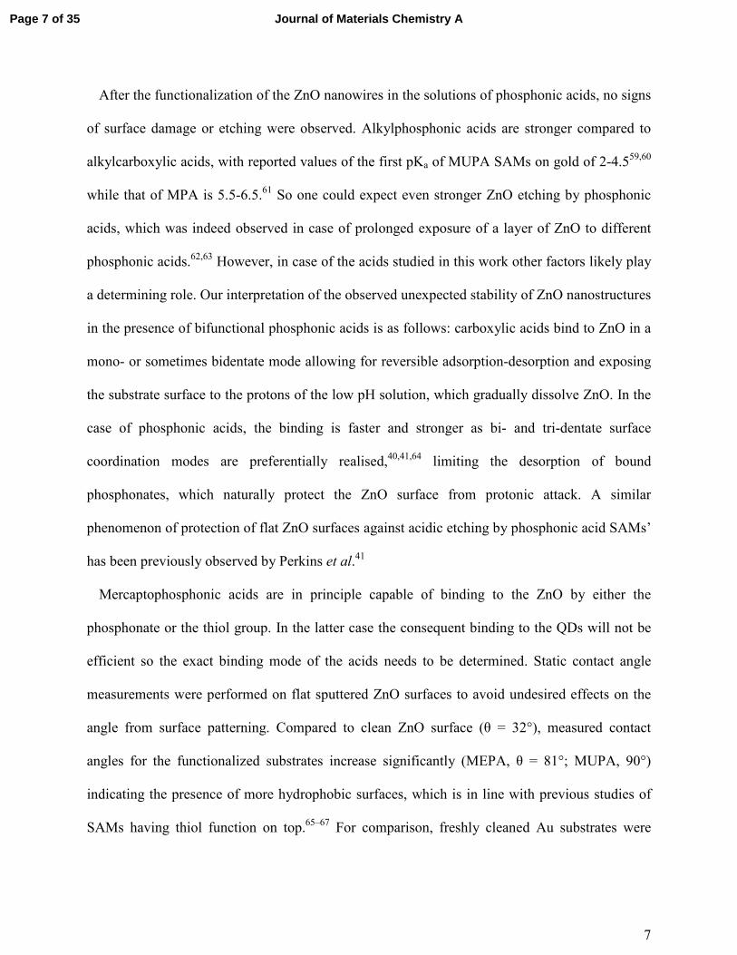
being hard bases in contrast to soft thiol groups (Figure 2).
Figure 2. Scheme of MEPA binding to different surfaces. Thiol binding to the Au surface may
lead to dimerization of the linker molecule via formation of hydrogen bonds.
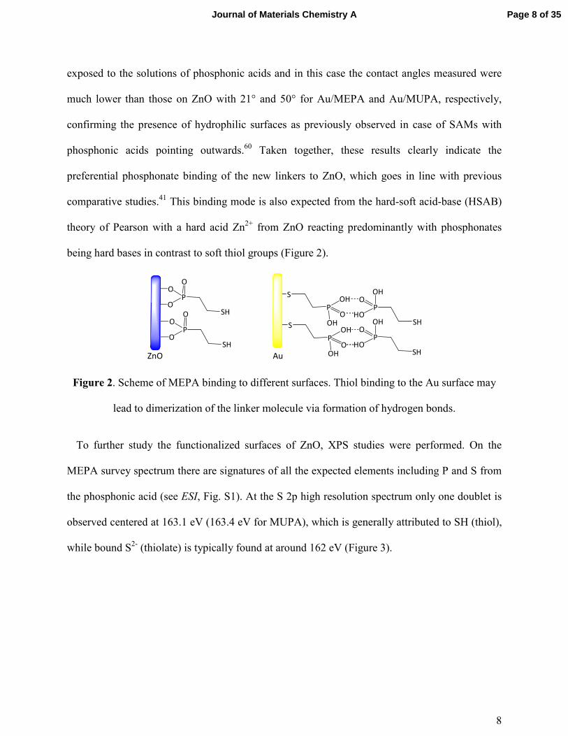
To further study the functionalized surfaces of ZnO, XPS studies were performed. On the
MEPA survey spectrum there are signatures of all the expected elements including P and S from
the phosphonic acid (see ESI, Fig. S1). At the S 2p high resolution spectrum only one doublet is
observed centered at 163.1 eV (163.4 eV for MUPA), which is generally attributed to SH (thiol),
while bound S2- (thiolate) is typically found at around 162 eV (Figure 3).
SH
PO
O
O
S
P
OH
OH
O
S
P
OH
OH
OSH
P
OH
HO
O
SH
P
OH
HO
O
ZnO Au
SH
PO
O
O
Page 8 of 35Journal of Materials Chemistry A
9
Figure 3. High resolution XPS spectrum of S 2p in ZnO/MEPA.
The fact that 100% of sulfur in ZnO/MEPA layers is in thiol form is important for the
subsequent assembly of the QDs: under certain conditions, thiol compounds are capable of
forming disulfide bridges rendering the attachment of QDs inefficient, while in our case the
SAMs are disulfide-free. Moreover, the observed XPS signal serves as an additional
corroboration of the SAMs bound by phosphonate. Another important observation is the absence
of signal of undesired oxidized sulfur species at 168 eV, which were previously observed in
some mercaptophosphonic SAMs.67 The elemental ratio of S and P for both assembled
phosphonic acid monolayers on ZnO is close to 1.4, which is higher than unity expected from the
mere stoichiometry. It can be explained by partial signal attenuation because of the deeper
phosphonate groups partially masked by exterior thiols.
In the case of layers of linker molecules assembled on gold, two signals of S 2p3/2 sulfur are
observed, at 162.2 and 163.4 eV (161.7 and 163.3 eV for MUPA) corresponding to 65% of
bound (thiolate) and 35% unbound (thiol) forms, respectively (Fig. S2, ESI). Such behavior can
be explained by a different binding mode of mercaptophosphonic acids assembled on Au with
170 168 166 164 162 160 158
S 2p1/2
CP
S,
a.u
.
Binding energy, eV
S 2p3/2
Page 9 of 35 Journal of Materials Chemistry A
10
subsequent possibility of intermolecular hydrogen bonding between the exterior phosphonic
groups (Fig. 2).54 This corroborates the contact angle data, indicating that on ZnO surfaces
phosphonate surface binding is preferential while on Au the binding occurs via sulfur.
Assembly of QDs on mercaptophosphonic acid functionalised metal oxides. Following the
successful formation of MEPA and MUPA linker layers on NMOs, ternary semiconductor
quantum dots were deposited by self-assembly from solution. Colloidal CuInS2 QDs of 3-4 nm
size covered with native dodecanethiol ligands were synthesized according to standard
procedures.68 The colour of both ZnO and TiO2 electrodes changes to dark brown after overnight
immersion into a chloroform solution of CuInS2 nanocrystals and abundant rinsing with an
appropriate solvent, which is also reflected by the absorption spectrum of ZnO after the QD
deposition (Figure 4). The difference of the spectra before and after assembly corresponds to the
contribution of the CuInS2 QDs to the absorption spectrum (see Fig. S7). We also note a weak
photoluminescence signal centered at 820 nm corresponding to the emission of the CuInS2
nanocrystals.
Page 10 of 35Journal of Materials Chemistry A
11
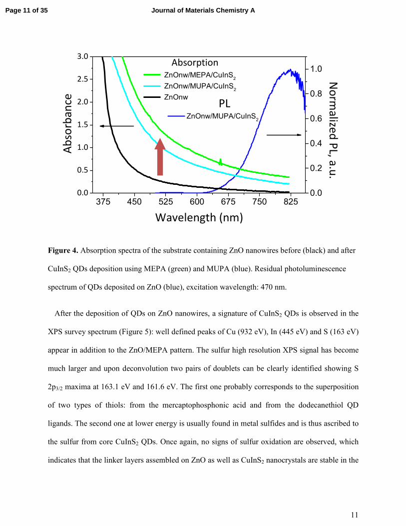
Figure 4. Absorption spectra of the substrate containing ZnO nanowires before (black) and after
CuInS2 QDs deposition using MEPA (green) and MUPA (blue). Residual photoluminescence
spectrum of QDs deposited on ZnO (blue), excitation wavelength: 470 nm.
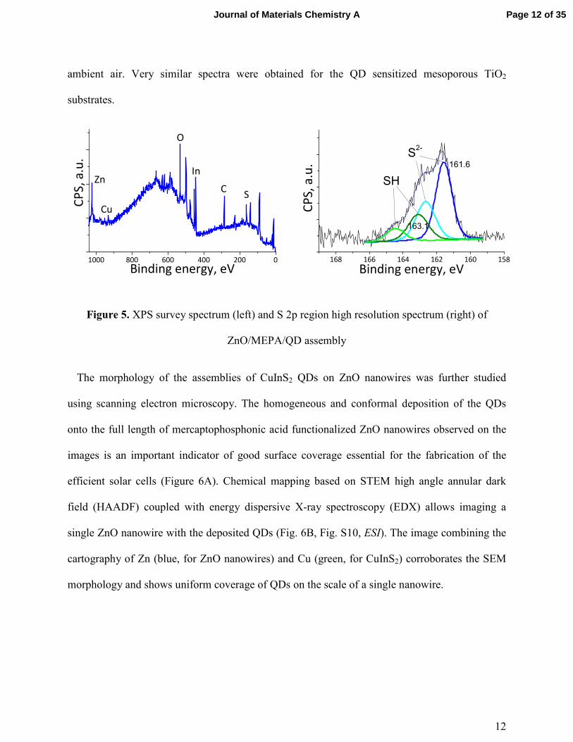
After the deposition of QDs on ZnO nanowires, a signature of CuInS2 QDs is observed in the
XPS survey spectrum (Figure 5): well defined peaks of Cu (932 eV), In (445 eV) and S (163 eV)
appear in addition to the ZnO/MEPA pattern. The sulfur high resolution XPS signal has become
much larger and upon deconvolution two pairs of doublets can be clearly identified showing S
2p3/2 maxima at 163.1 eV and 161.6 eV. The first one probably corresponds to the superposition
of two types of thiols: from the mercaptophosphonic acid and from the dodecanethiol QD
ligands. The second one at lower energy is usually found in metal sulfides and is thus ascribed to
the sulfur from core CuInS2 QDs. Once again, no signs of sulfur oxidation are observed, which
indicates that the linker layers assembled on ZnO as well as CuInS2 nanocrystals are stable in the
375 450 525 600 675 750 8250.0
0.2
0.4
0.6
0.8
1.0
PL ZnOnw/MUPA/CuInS
2
AbsorptionA
bso
rba
nce
No
rma
lized
PL, a
.u.
Wavelength (nm)
0.0
0.5
1.0
1.5
2.0
2.5
3.0
ZnOnw/MEPA/CuInS2
ZnOnw/MUPA/CuInS2
ZnOnw
Page 11 of 35 Journal of Materials Chemistry A
12
ambient air. Very similar spectra were obtained for the QD sensitized mesoporous TiO2
substrates.
Figure 5. XPS survey spectrum (left) and S 2p region high resolution spectrum (right) of
ZnO/MEPA/QD assembly
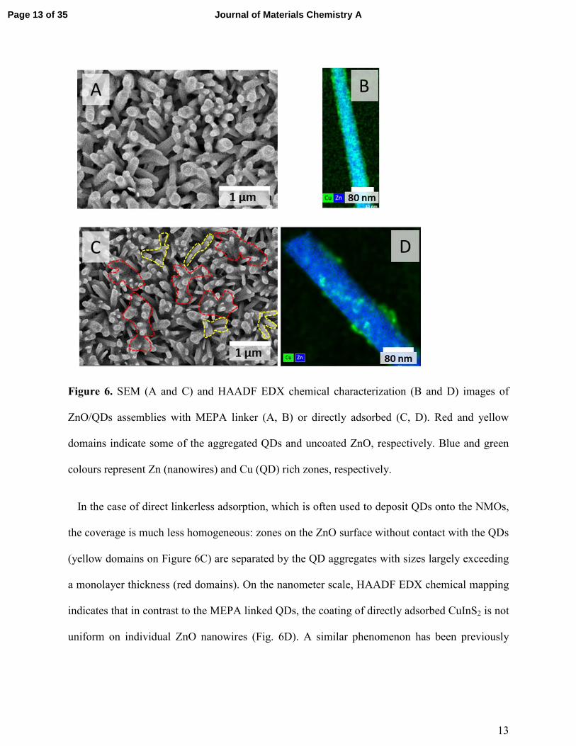
The morphology of the assemblies of CuInS2 QDs on ZnO nanowires was further studied
using scanning electron microscopy. The homogeneous and conformal deposition of the QDs
onto the full length of mercaptophosphonic acid functionalized ZnO nanowires observed on the
images is an important indicator of good surface coverage essential for the fabrication of the
efficient solar cells (Figure 6A). Chemical mapping based on STEM high angle annular dark
field (HAADF) coupled with energy dispersive X-ray spectroscopy (EDX) allows imaging a
single ZnO nanowire with the deposited QDs (Fig. 6B, Fig. S10, ESI). The image combining the
cartography of Zn (blue, for ZnO nanowires) and Cu (green, for CuInS2) corroborates the SEM
morphology and shows uniform coverage of QDs on the scale of a single nanowire.
168 166 164 162 160 1581000 800 600 400 200 0
CP
S,
a.u
.
SH
Binding energy, eV
161.6
163.1
S2-
CP
S,
a.u
.
Cu
S
In
C
O
Binding energy, eV
Zn
Page 12 of 35Journal of Materials Chemistry A
13
Figure 6. SEM (A and C) and HAADF EDX chemical characterization (B and D) images of
ZnO/QDs assemblies with MEPA linker (A, B) or directly adsorbed (C, D). Red and yellow
domains indicate some of the aggregated QDs and uncoated ZnO, respectively. Blue and green
colours represent Zn (nanowires) and Cu (QD) rich zones, respectively.
In the case of direct linkerless adsorption, which is often used to deposit QDs onto the NMOs,
the coverage is much less homogeneous: zones on the ZnO surface without contact with the QDs
(yellow domains on Figure 6C) are separated by the QD aggregates with sizes largely exceeding
a monolayer thickness (red domains). On the nanometer scale, HAADF EDX chemical mapping
indicates that in contrast to the MEPA linked QDs, the coating of directly adsorbed CuInS2 is not
uniform on individual ZnO nanowires (Fig. 6D). A similar phenomenon has been previously
Page 13 of 35 Journal of Materials Chemistry A
14
observed in the case of mesoporous TiO2 electrodes sensitized by directly adsorbed CdSe QDs,
which aggregated in the pores and on top of the TiO2 layer.32,69
Preliminary ex situ ligand exchange of colloidal CuInS2 QDs with mercaptophosphonic acids
has been attempted to explore this alternative route of their deposition on the NMOs. However,
adding the solution of QDs in chloroform to the solution of MEPA in formamide followed by
stirring resulted in the precipitation of the QDs. We attribute the observed aggregation of the
QDs to interparticle hydrogen bonding between of the phosphonic acid groups at outer
extremities of the ligand shell. This interpretation is supported by our study of
mercaptophosphonic acids binding to Au (vide supra) and by other previous results of
intermolecular binding of similar compounds.54,55,59 For this reason, all further work was
performed using TiO2 and ZnO pre-functionalized by mercaptophosphonic acids rather than
using the ex situ ligand exchange approach.
Charge transfer dynamics. The dynamics of charge transfer from photoexcited nanocrystals
to the NMOs has been investigated by means of time-resolved photoluminescence (PL) studies.
In order to investigate the influence of linkers on the efficiency of charge transfer, several
systems were assembled and studied: we used mesoporous TiO2 and ZnO nanowires as
substrates with CuInS2 QDs deposited using first linkerless attachment followed by linker
assisted assembly using MPA, MEPA, or MUPA. The PL quantum yield (QY) was measured for
all the systems studied. The relatively high QY of the QD film on fused silica substrate (SiO2)
(6.7%) drops significantly to 0.1-0.8% for the systems deposited on TiO2 and ZnO substrate. On
SiO2 substrates the excitons generated in the QDs upon the absorption of light can decay either
radiatively or non-radiatively on surface or internal defects. In the assemblies with NMOs a third
exciton de-excitation pathway appears: injection of the excited electron of CuInS2 into the
Page 14 of 35Journal of Materials Chemistry A
15
conduction band of the TiO2 or ZnO. This electron transfer pathway competes with radiative
recombination thus decreasing the overall QY of the QDs. The QY decrease in assemblies can
therefore serve as an indirect indicator of electron transfer between excited CuInS2 QDs and
TiO2 or ZnO. At the same time it cannot be utilized directly to quantify its efficiency because of
other possible recombination pathways appearing upon QD-NMO binding via the linkers. For
instance, it cannot be excluded that new surface defect states are formed because of the
perturbation of the initial QD ligand shell by thiol groups of the ligands.
In order to quantify the charge injection efficiency in the assemblies, transient PL studies were
performed using time-correlated single photon counting at an excitation wavelength of 470 nm.
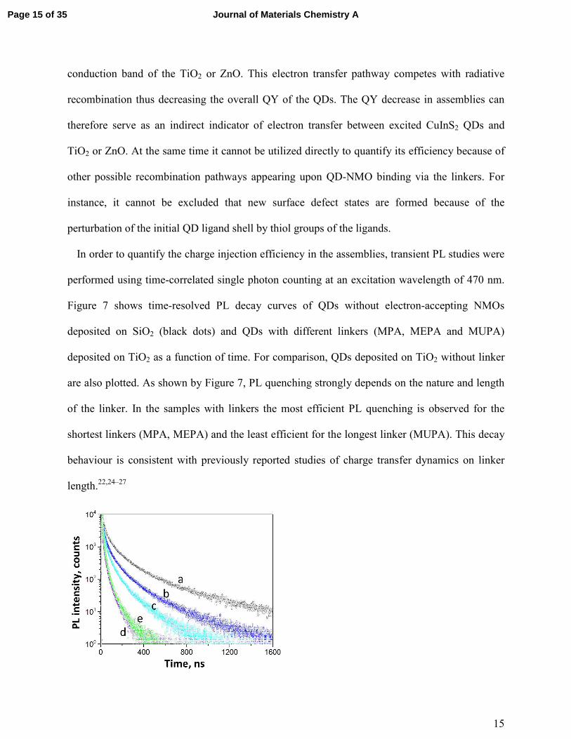
Figure 7 shows time-resolved PL decay curves of QDs without electron-accepting NMOs
deposited on SiO2 (black dots) and QDs with different linkers (MPA, MEPA and MUPA)
deposited on TiO2 as a function of time. For comparison, QDs deposited on TiO2 without linker
are also plotted. As shown by Figure 7, PL quenching strongly depends on the nature and length
of the linker. In the samples with linkers the most efficient PL quenching is observed for the
shortest linkers (MPA, MEPA) and the least efficient for the longest linker (MUPA). This decay
behaviour is consistent with previously reported studies of charge transfer dynamics on linker
length.22,24–27
Page 15 of 35 Journal of Materials Chemistry A
16
Figure 7. PL kinetics of CuInS2 without electron-accepting NMOs i.e. on SiO2 (a), CuInS2
with different linkers: MUPA (b), MEPA (c), MPA (d) deposited on TiO2 as function of time.
For comparison, linkerless CuInS2 deposited on TiO2 (e) is also plotted.
In the previous literature on time-resolved PL of ternary nanoparticles three exponential fits
were performed to describe the decay.68,70–74 Here, the three component decay lifetimes found
are 13, 93 and 486 ns for CuInS2 nanoparticles on SiO2 without electron-accepting NMOs, the
details about the fitting parameters are given in Table S1, supplementary information. The fastest
decay lifetime is typically associated with surface-related traps because of their shallow nature
and the slower decay times are due to intrinsic defect related trap states.68,70,71 Accordingly, the
observed fast (13 ns) and slower decay components (93 ns, 486 ns) can be attributed to radiative
recombination processes of QD surface defect states and of defect related donor-acceptor pairs,
respectively.72–74 Recently, these two longer lifetimes were further assigned to two distinct
processes: the shorter one to recombination processes of nearest donor-acceptor pairs and the
longer one to next-to-closest donor-acceptor neighbours.71 These donor and acceptor states in
ternary CuInS2 nanocrystals are believed to appear due to In, Cu antisite defects or sulfur
vacancies.74
The average PL decay lifetime was calculated using the weighted average of the fitted
exponentials as follows:
� = ���� + ���� + ������ + �� + �� (1)
where τ1, τ2, τ3 are the lifetimes of the fitted components and α1, α2, α3 the corresponding pre-
exponential factors. The large average lifetime (172 ns) we obtain for our ternary CuInS2
nanocrystals compared to that of binary nanocrystals confirms that intrinsic defect states are
mainly responsible for the emission we observe.5
Page 16 of 35Journal of Materials Chemistry A
17
The PL decay transients for the assemblies on NMOs can also be fitted with three exponentials
(Table S1 for detail). The average PL lifetimes measured for the QDs deposited on TiO2 or ZnO
were found to be generally much shorter than those on SiO2 (Figure 7, Table 1). This faster
decay is related to the electronic interaction between components of the assemblies with a
significant part of the excited electrons of QDs being rapidly injected into the conduction band of
TiO2 or ZnO rather than undergoing radiative decay observed for the samples on SiO2, which is
in line with the observed decrease of PL QY. If we assume that shortening of the QD lifetime is
exclusively due to electron transfer from CuInS2 to TiO2 or ZnO, neglecting potential
perturbation of the ligand shell as well as other possible secondary effects in the assemblies, then
the rate constant for electron transfer kET can be determined. Previous studies have estimated kET
using � � = 1/�(���������/������) − 1/�(������).13,27,51,75,76 However, such an approach
assumes a monoexponential decay in order to convert lifetime to rate constant and is therefore
not suitable for our data with its multiexponential decay. As we are trying to determine electron
transfer from the nanocrystal to the substrate, it is the additional rate of decay of PL due the TiO2
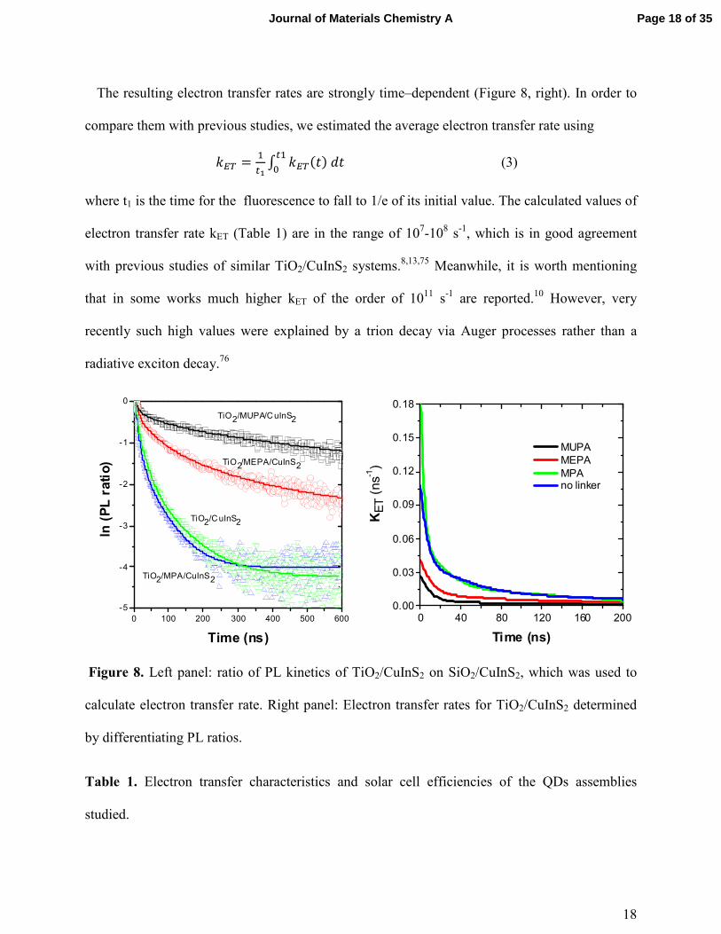
substrate that is of interest. We determine this by calculating the natural logarithm of the ratio of
the PL decay of QDs with electron-accepting NMO (i.e. on TiO2) to the PL decay of QDs
without NMO (on SiO2). In the absence of electron transfer, the resulting graph vs time would be
flat. Nonlinearity observed in our case indicates presence of an additional decay, which we
assign to a time-dependent electron transfer process (Figure 8, left). By fitting the data on the
figure with a three exponential decay followed by differentiation we can determine this electron
transfer rate according to77
� �(�) = − ��� � � !"#$%&'$()*+
"#$%&'$(,-.//01 (2)
Page 17 of 35 Journal of Materials Chemistry A
18
The resulting electron transfer rates are strongly time–dependent (Figure 8, right). In order to
compare them with previous studies, we estimated the average electron transfer rate using
� � = ��2 3 � �(�)4���
5 (3)
where t1 is the time for the fluorescence to fall to 1/e of its initial value. The calculated values of
electron transfer rate kET (Table 1) are in the range of 107-108 s-1, which is in good agreement
with previous studies of similar TiO2/CuInS2 systems.8,13,75 Meanwhile, it is worth mentioning
that in some works much higher kET of the order of 1011 s-1 are reported.10 However, very
recently such high values were explained by a trion decay via Auger processes rather than a
radiative exciton decay.76
Figure 8. Left panel: ratio of PL kinetics of TiO2/CuInS2 on SiO2/CuInS2, which was used to
calculate electron transfer rate. Right panel: Electron transfer rates for TiO2/CuInS2 determined
by differentiating PL ratios.
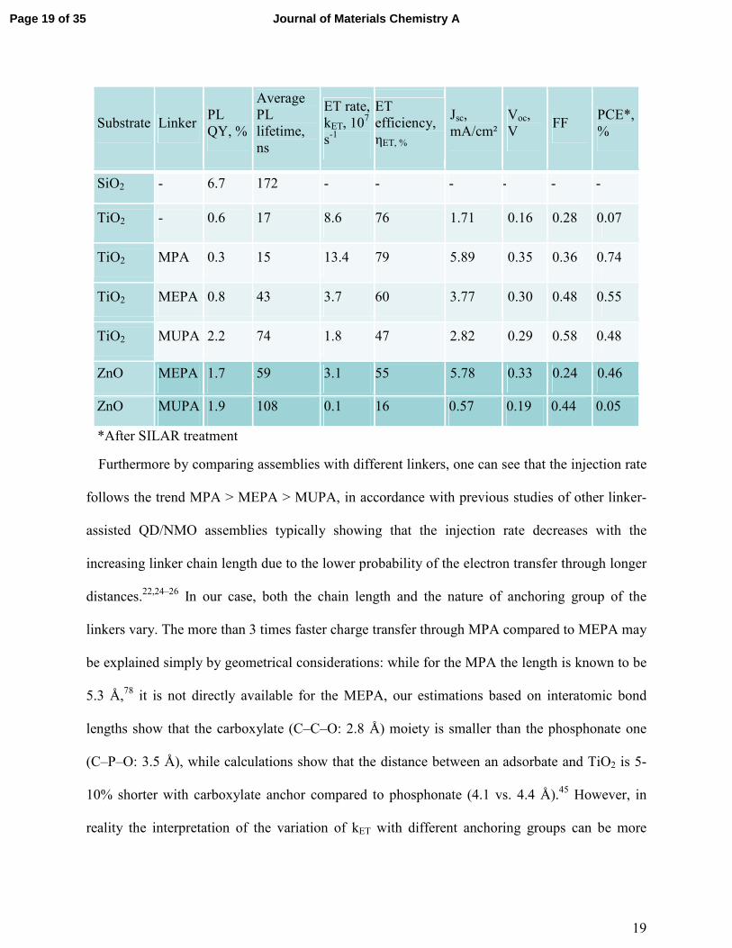
Table 1. Electron transfer characteristics and solar cell efficiencies of the QDs assemblies
studied.
0 40 80 120 160 2000.00
0.03
0.06
0.09
0.12
0.15
0.18
KET (ns-1
)
Time (ns)
MUPA
MEPA
MPA no linker
0 100 200 300 400 500 600
-5
-4
-3
-2
-1
0
TiO2/MPA/CuInS2
TiO2/MEPA/CuInS2
TiO2/CuInS2
ln (PL ratio)
Time (ns)
TiO2/MUPA/CuInS2
Page 18 of 35Journal of Materials Chemistry A
19
Substrate Linker PL QY, %
Average PL lifetime, ns
ET rate, kET, 107 s-1
ET efficiency, ηET, %
Jsc, mA/cm²
Voc, V
FF PCE*, %
SiO2 - 6.7 172 - - - - - -
TiO2 - 0.6 17 8.6 76 1.71 0.16 0.28 0.07
TiO2 MPA 0.3 15 13.4 79 5.89 0.35 0.36 0.74
TiO2 MEPA 0.8 43 3.7 60 3.77 0.30 0.48 0.55
TiO2 MUPA 2.2 74 1.8 47 2.82 0.29 0.58 0.48
ZnO MEPA 1.7 59 3.1 55 5.78 0.33 0.24 0.46
ZnO MUPA 1.9 108 0.1 16 0.57 0.19 0.44 0.05
*After SILAR treatment
Furthermore by comparing assemblies with different linkers, one can see that the injection rate
follows the trend MPA > MEPA > MUPA, in accordance with previous studies of other linker-
assisted QD/NMO assemblies typically showing that the injection rate decreases with the
increasing linker chain length due to the lower probability of the electron transfer through longer
distances.22,24–26 In our case, both the chain length and the nature of anchoring group of the
linkers vary. The more than 3 times faster charge transfer through MPA compared to MEPA may
be explained simply by geometrical considerations: while for the MPA the length is known to be
5.3 Å,78 it is not directly available for the MEPA, our estimations based on interatomic bond
lengths show that the carboxylate (C–C–O: 2.8 Å) moiety is smaller than the phosphonate one
(C–P–O: 3.5 Å), while calculations show that the distance between an adsorbate and TiO2 is 5-
10% shorter with carboxylate anchor compared to phosphonate (4.1 vs. 4.4 Å).45 However, in
reality the interpretation of the variation of kET with different anchoring groups can be more
Page 19 of 35 Journal of Materials Chemistry A
20
complex due to the specific interaction of these groups with the TiO2 surface realizing different
binding modes (mono-, bi- or tridentate) and bond strengths involved. Various studies comparing
the charge transfer in the case of the organic dyes attached to TiO2 substrates by carboxylic and
phosphonic anchors come to contradictory conclusions: some groups report faster injection
through phosphonates,45,46 while other through carboxylates.47–49,79 Most likely, the relative rates
depend strongly on the structure of the injecting moiety.80 Meanwhile, it should be noted that all
these studies have been made on the organic adsorbates conjugated to TiO2 surface, with the
electron injected directly through the anchoring group. In this case, slower injection through
phosphonates can be explained by lower electronic coupling of the dye with the anchor (and
thus TiO2 surface) because of the tetrahedral sp3 geometry of the phosphorus.49,79 In the case of
QDs attached to the TiO2, the linker is saturated, electron injection occurs essentially by
tunnelling and thus conjugation effects should be less applicable. A more systematic theoretical
study of the mechanism of charge transfer from QDs using linkers with different anchoring
groups is necessary.
In contrast to TiO2, charge injection from CuInS2 into the ZnO nanowires is much less studied.
The only values available for the ZnO/CuInS2:Zn system lie in the range of 107-108 s-1,15 which
is comparable to our results. Recent detailed photophysical studies by Židek et al. of the
ZnO/CdSe systems showed an ultrafast charge injection of the order of 1012 s-1,81,82 however care
should be taken while comparing CuInS2 and CdSe based systems: first, it is known that
contrary to the former, binary CdSe QDs exhibit band edge emission with much faster decay
rates on the order of tens of nanoseconds. Moreover, we have to consider that in the reported
CdSe based systems electron injection coexists with Auger recombination. Therefore, we can
Page 20 of 35Journal of Materials Chemistry A
21
assume that the mechanisms of charge injection in the two cases are quite different, which can
explain the discrepancy in observed kET.
The high electron injection rate (8.6 × 10⁷ s-1) observed for CuInS2 deposited via direct
adsorption onto TiO2 can be explained by the fact that such a linkerless mode provides for the
shortest distance between the QD and NMO thus avoiding the electron tunnelling through a
linker chain. Similar observations of higher injection rates were previously made in the case of
CdSe nanocrystals directly adsorbed on TiO2.33,69,83 However, as will be shown below, the solar
cell device efficiency obtained with this linkerless system is very low compared to the systems
with linkers.
In order to calculate the electron transfer efficiency ηET, we integrated the entire decay of QDs
on SiO2 and on electron-accepting NMOs. We then used the difference of area to calculate the
electron transfer efficiency ηET as follows84
6 � = 1 − 3 789:;<=>?/@;>��3 789:;A=>?�� (4)
where IQD on TiO2 and IQD on SiO2 are intensity decays of QDs on NMOs and on SiO2, respectively.
The electron transfer efficiencies calculated for the systems based on TiO2 show high values with
ηET = 79% for the best TiO2/MPA/CuInS2 assembly (Table 1), which are very close to the
previously reported values of CuInS2 nanocrystals deposited on TiO2.75 For systems based on
ZnO, the electron transfer efficiency is comparably low. This may be due to fact that ZnO
nanowires can present a large number of surface trap states compared to TiO2: transfer efficiency
in ZnO/QD systems depends strongly on the photoelectron recombination at the interface,
therefore defects on the surfaces of both ZnO and QDs could act as traps for the photoelectron
and thus lower the overall injection efficiency.85 Overall, fast electron injection together with
Page 21 of 35 Journal of Materials Chemistry A
22
high electron transfer efficiency obtained for the assemblies studied demonstrate the high
potential of these systems for use in photovoltaic cells.
Photovoltaic behavior. To investigate the effects of electron transfer rates on the photovoltaic
performance, QDSSCs based on the assemblies studied above have been fabricated and tested
under simulated sunlight using standard AM 1.5G conditions. Functionalization of mesoporous
TiO2 by new mercaptophosphonic linkers and deposition of QDs was followed by the coating of
the assemblies with an inorganic CdS passivation layer. Such layer was deposited by successive
ionic layer adsorption and reaction (SILAR) method consisting in consecutive dipping of the
substrate into the solutions with cationic and anionic precursors. In addition to slight contribution
of CdS coating to the light absorption (see Fig. S8), CdS and ZnS layers were shown to
significantly reduce recombination in the QDSSCs due to the suppression of undesired electron
transfer from the QD to the electrolyte because of the type I band alignment at the interface
QD/SILAR layer representing a potential energy barrier.18 The cell was completed by
introduction of the polysulfide electrolyte and CuxS counter-electrode. Unlike classical
iodide/triiodide electrolyte used in dye sensitized cells, this former does not etch the surface of
QDs and thus is preferentially used in QDSSCs.
Generally decent photovoltaic conversion efficiencies (PCEs) of 0.4-0.5% were achieved for
the cells, with open circuit voltage, Voc, values of the order of 0.3 V (Table 1, Fig. S11). The
parameter, which changes most significantly with the nature of the ligands, is the short circuit
current, Jsc. Interestingly, the trend in the variation of Jsc generally follows the calculated charge
injection efficiency with linkers having shorter chain length showing higher current and
efficiency. One drastic exception from this trend is CuInS2 directly adsorbed on TiO2 having one
of the fastest injection rates but also the lowest efficiency among all TiO2 based cells tested. The
Page 22 of 35Journal of Materials Chemistry A
23
explanation for this observation may come from the observed incomplete and non-homogeneous
coverage of the nanostructured metal electrodes by the QDs (Figure 6C, D). Consequently, even
though the injection of QDs in close contact with the electrode is rapid, a significant part of the
QDs is situated within the aggregates far from the electrode, increasing the losses and resulting
in low current and Voc. The highest PCE was achieved using classical mercaptopropionic acid as
a linker in accordance with the trend observed in electron transfer rate and efficiency.
There are very few examples of solar cells based on ZnO nanowire electrodes sensitized with
colloidal QDs. All of them have been fabricated using ex situ ligand exchange with a linker
molecule or electrophoresis for deposition and show relatively modest efficiencies (below 1%)
compared to their TiO2 counterparts.15,30,86,87 This can be explained by a high defect density in
the solution grown ZnO nanowires but also by the impossibility to use classical MPA ligands for
the direct functionalization of the nanowires because of the inevitable surface etching. By using
ZnO functionalization with the novel bifunctional linker MEPA we achieve 0.46% using as-
synthesized ternary CuInS2 QDs.
In summary, new mercaptophosphonic linkers for the homogeneous deposition of quantum
dots on nanostructured NMOs were developed. XPS studies showed that mercaptophosphonic
acids of various lengths form monolayers with the phosphonic group bound to the NMOs and the
thiol function pointing outwards. The deposition of ternary CuInS2 quantum dots on the
mercaptophosphonic SAMs is efficient and uniform as demonstrated by XPS, SEM, HAADF-
EDX and UV-vis absorption studies. Charge transfer processes investigated by time-resolved PL
studies show that the electron injection from the QDs to TiO2 or ZnO occurs at fast rates of 107-
108 s-1 with high transfer efficiencies of 50-80% and strong dependence on the linker length and
nature of the anchoring group. Photovoltaic cells based on ternary QDs on TiO2 and ZnO NMOs
Page 23 of 35 Journal of Materials Chemistry A
24
attached via the novel mercaptophosphonic acid linkers result in PCEs of 0.4-0.6%. The
efficiencies follow the trend observed in the charge transfer studies: shorter linkers lead to better
injection and thus increased Jsc, which results in higher overall efficiency. The studied
phosphonic acid based linkers result in slightly lower kET and PCE compared to
mercaptopropionic acid, probably due to the different binding geometry and eventually more
efficient electron transfer via the carboxylate function. On the other hand, contrary to
mercaptocarboxylic acids the investigated mercaptophosphonic acids provide an efficient way to
functionalize pH-sensitive ZnO nanowires with a variety of nanomaterials. Because of the high
binding strength owing to multidentate coordination through the phosphonic acid group, they
rapidly functionalize the surface of ZnO nanostructures without detectable etching damages
induced by the acidic solution. Linkerless attachment of the CuInS2 nanocrystals (direct
adsorption) leads to fast electron transfer but the corresponding PCE is low due to the
inhomogeneous and incomplete coverage of the NMOs. Further improvement of the photovoltaic
properties can be expected through the optimization of the light-harvesting properties (e.g. via
the adsorption of multiple layers of QDs) and nanocrystal surface passivation (e.g. via Zn or Cd
cation exchange).7
Experimental details
Synthesis. 2-Mercaptoethyl phosphonic acid (MEPA) was synthesized according to the
literature procedure.88 Triphenylmethanethiol (4.28 g, 15.4 mmol) was added to NaH (0.4 g, 15
mmol) in 130 ml dry tetrahydrofurane (THF), yielding a yellow solution. (2-
Bromoethyl)phosphonic acid diethyl ester (2.5 ml, 14 mmol) was added and the solution stirred
for 1 h. The excess NaH was quenched with 13 ml of water. The resulting mixture was
Page 24 of 35Journal of Materials Chemistry A

25
evaporated to ca. 15 ml, dissolved in 50 ml of water, and extracted with 3 x 80 ml of CH2Cl2.
The organic layer was concentrated by rotary evaporation and dried under vacuum. Upon
trituration with 20 ml of diethyl ether, a white solid formed. The mixture was cooled to -78°C
and filtered. After rinsing with cold (-78°C) diethyl ether, the white product, diethyl (2-
tritylsulfanylethyl)phosphonate was dried (5.2 g, 84% yield). 1H NMR (200 MHz, CDCl3): 7.24
(m, 15H), 3.88 (m, 4H), 2.33 (m, 2H), 1.62 (m, 2H), 1.15 (t, 6H).
To remove the trityl protection group, the product was dissolved in 25 ml of trifluoroacetic
acid (TFA). Triethylsilane was added dropwise to the rapidly stirred solution until the yellow
colour was gone and a white solid precipitated. Once the precipitate was removed via vacuum
filtration, the TFA was evaporated to yield a slightly brown oil. The oil was transferred to a flask
equipped with a Dean-Stark trap and condenser and hydrolyzed in 75 ml of refluxing 5 M HCl
for 72 h. The aqueous layer was washed with 2x100 ml of chloroform and was concentrated by
rotary evaporation and dried in vacuo to yield MEPA, an off-white solid (1.2 g, 71% yield). 1H
NMR (200 MHz, D2O) 2.73 (m, 2H), 2.05 (m, 2H), 1.21 (d, 1H).
11-Mercaptoundecyl phosphonic acid (MUPA) was synthesized according to the literature
procedure.55 Freshly distilled triethylphosphite (5.4 ml, 31.2 mmol) and 11-bromo-1-undecene (3
g, 12.9 mmol) were refluxed for 24 h under Ar flux. The solution was cooled, 20 ml of cold
deionized water was added and the mixture was stirred for 3 h. The organic compound was
extracted by chloroform (2x20 ml), washed with water, brine, dried over MgSO4 and purified by
column chromatography to yield 2.4 g (64% yield) of yellowish oil. 2 g of the oil were mixed
with thioacetic acid (1.89 ml, 27.3 mmol) and AIBN (5 mg, 0.03 mmol) and exposed to UV light
using 35 W mercury lamp in a photochemical reactor under stirring and cooling for 8 h.
Saturated sodium hydrocarbonate solution (20 ml) was slowly added and the organic phase was
Page 25 of 35 Journal of Materials Chemistry A
26
washed with water and brine to yield an orange yellow oil followed by its purification by column
chromatography to result in 1.37 g (52% yield) of diethyl 11-(acetylthio)undecylphosphonate.
This thioether has been hydrolyzed by dissolution in ethanol and concentrated HCl (35-37%) and
refluxing under Ar for 7 h and concentrated by rotary evaporator to give 0.965 g (92% yield) of
diethyl 11-mercaptoundecylphosphonate. The ester (0.8 g, 2.3 mmol) was hydrolyzed by adding
concentrated HCl and refluxing for 19 h to finally result in 11-mercaptoundecyl phosphonic acid
after drying in vacuo. 1H NMR (200 MHz, CDCl3): 7.17 (br, (2H), PO(OH)2), 2.52 (q, 2H,
CH2SH), 1.5-1.9 (m, 6H), 1.2-1.5 (m, 16H).
ZnO nanowires were grown according to published techniques:89 indium-doped tin oxide
(ITO) glass was cleaned by sonication in a deionized (DI) water, ethanol and acetone, followed
by 10 min. treatment in an UV ozone chamber. The substrate was then spin-coated with 5 mM
zinc acetate solution in ethanol followed by thermal treatment at 300 °C for 20 min. The seeded
substrate is then immersed into the ZnO growth solution (25 mM zinc nitrate, 12.5 mM
hexamethylenetetramine (HMTA), 5 mM PEI (end-capped, molecular weight 800 g/mol LS,
Aldrich), and 0.4 M ammonium hydroxide). The container was covered heated to 90°C. The
resulting nanowire arrays were rinsed with DI water and calcined in air at 450 °C for 30 min to
remove any residual organics.
QD synthesis. Synthesis of colloidal CuInS2 QDs roughly follows established route:68 indium
acetate (1.17 g, 4 mmol) is mixed with copper(I) iodide (0.760 g, 4 mmol) and 1-dodecanethiol
(DDT, 15 mL) in a three-necked flask. The reaction mixture is degassed under vacuum for 5 min
and purged with argon three times. The flask is heated to 100°C for 1 h for the complexation.
The temperature is then rapidly raised to 230°C for 15-30 min. After cooling, the colloidal QDs
are isolated by precipitating by addition of acetone, centrifuging, decanting the supernatant and
Page 26 of 35Journal of Materials Chemistry A
27
redispersing in chloroform. This purification procedure is typically repeated 3 times to get rid of
the free DDT and unreacted byproducts.
Characterisation. 1H NMR spectra were recorded on a Bruker AC 200 MHz spectrometer
using deuterated solvents containing TMS as internal standard. A Zeiss Ultrascan 55 scanning
electron microscope (SEM) was used to take images of the nanowires. Scanning transmission
electron microscopy (STEM) with HAADF and EDX was done on FEI-Titan microscopes
operated at 300 kV. X-ray photoelectron spectroscopy (XPS) measurements were performed on
an SSI S-Probe spectrometer from (Euroscan SA) using a monochromatic Al Kα X-ray source
(1486.6 eV) at a constant dwell time of 100 ms and pass energy of 50 eV. The core-level signals
were obtained at a photoelectron takeoff angle of 35°. The pressure in the analysis chamber was
maintained at 10−9 mbar or lower. All peaks were adjusted using the C 1s peak at 284.6 eV to
correct the binding energies for the charge shift. Photoelectrons were detected using a
hemispherical analyzer, with an angular acceptance of 30° and an energy resolution of 850 meV.
Elemental quantification was performed using CasaXPS software by the analysis of the integral
intensity of each core- level line weighed by its corresponding Scofield sensitivity factor
available from the internal database of the software. The contact angle measurements were
performed on flat layers of ZnO sputtered on glass by using Krüss drop shape analyser.
Photophysical studies. Absorption measurements were carried out using Varian Cary 300
UV-vis spectrophotometer and PL spectrum was obtained using Edinburgh Photonics Instrument
FLS980. The excitation wavelengths of 470 nm were used for PL measurements. The PL
lifetimes were measured by exciting the samples using 470 nm PicoQuant picosecond pulsed
lasers and PL was detected at 770 nm using time correlated single photon counting with time
resolution of ~200 ps. Further experimental details can be found elsewhere.
Page 27 of 35 Journal of Materials Chemistry A
28
QDs deposition. Freshly activated substrates of mesoporous TiO2 films (10 µm, Solaronix) or
ZnO nanowires were immersed into 5 mM DMSO solutions of MEPA and MUPA or aqueous
solution of 1 M MPA with 0.1 M H2SO4 for 12 h. After the removal, the substrates were
thoroughly rinsed with a pure solvent and dried under the Ar stream. Following the
functionalization, the substrates were immersed into the concentrated solutions of QDs in
chloroform for 24 h following by the abundant rinsing with fresh solvent and drying. The
sensitized substrates were coated by 10 layers of CdS by SILAR method (1 SILAR layer: 30 s
dip in 50 mM aqueous Cd(NO3)2, rinsing with water, 30 s dip in 50 mM aqueous Na2S, rinsing
with water).
Solar cell fabrication and testing. ZnO nanowire substrates were scraped to have an active
area of 0.36 cm². CuxS counter electrode was prepared from a brass sheet activated for 10 min. in
hot (70°C) concentrated HCl followed by dropping the polysulfide electrolyte solution (1 M S, 1
M Na2S, 0.1 M NaOH in H2O) and carefully rinsing with DI water. The cells were assembled
using Surlyn film (Solaronix, Switzerland) as a spacer; No mask was used, the active cell area
was 0.36 cm². Photovoltaic characteristics of the solar cells were evaluated using simulated AM
1.5 sunlight with an output power of 100 mW cm².
Acknowledgements. This work was supported by the Agence Nationale de la Recherche,
project QuePhélec (ANR-13-BS10-0011-01). The authors gratefully acknowledge Dr. Olivier
Renault at the Minatec Nanocharacterization platform for facilitating XPS measurements and Dr.
Pierre-Henri Jouneau from CEA/INAC/SP2M/LEMMA for helping with HAADF-EDX. MTS
and IDWS are thankful to ERC for financial support for exciton diffusion project, grant number
321305. AKB and IDWS also acknowledge financial support from EPSRC programme grant:
structured light, EP/J01771X.
Page 28 of 35Journal of Materials Chemistry A
29
Supporting information. Electronic supplementary information (ESI) available: XPS spectra,
details of the exponential fit of the PL decay transients, HAADF EDX images and other detailed
information. See DOI:
References
1 A. J. Nozik, M. C. Beard, J. M. Luther, M. Law, R. J. Ellingson and J. C. Johnson, Chem. Rev., 2010, 110, 6873–90.
2 J. B. Sambur, T. Novet and B. A. Parkinson, Science, 2010, 330, 63–6.
3 P. V Kamat, J. Phys. Chem. Lett., 2013, 4, 908–918.
4 K. Zhao, Z. Pan, I. Mora-Seró, E. Cánovas, H. Wang, Y. Song, X. Gong, J. Wang, M. Bonn, J. Bisquert and X. Zhong, J. Am. Chem. Soc., 2015, 137, 5602–5609.
5 D. Aldakov, A. Lefrançois and P. Reiss, J. Mater. Chem. C, 2013, 1, 3756.
6 H. McDaniel, N. Fuke, J. M. Pietryga and V. I. Klimov, J. Phys. Chem. Lett., 2013, 4, 355–361.
7 H. McDaniel, N. Fuke, N. S. Makarov, J. M. Pietryga and V. I. Klimov, Nat. Commun., 2013, 4, 1–10.
8 H. Mcdaniel, A. Y. Koposov, S. Draguta, N. S. Makarov, J. M. Pietryga and V. I. Klimov, J. Phys. Chem. C, 2014, 118, 16987–16994.
9 D. H. Jara, S. J. Yoon, K. G. Stamplecoskie and P. V Kamat, Chem. Mater., 2014.
10 P. K. Santra, P. V. Nair, K. G. Thomas and P. V. Kamat, J. Phys. Chem. Lett., 2013, 4, 722–729.
11 J. S. Niezgoda, E. Yap, J. D. Keene, J. R. Mcbride and S. J. Rosenthal, Nano Lett., 2014, 14, 3262–3269.
12 J. Luo, H. Wei, Q. Huang, X. Hu, H. Zhao, R. Yu, D. Li, Y. Luo and Q. Meng, Chem. Commun. (Camb)., 2013, 49, 3881–3.
Page 29 of 35 Journal of Materials Chemistry A
30
13 C.-C. Chang, J.-K. Chen, C.-P. Chen, C.-H. Yang and J.-Y. Chang, ACS Appl. Mater. Interfaces, 2013, 5, 11296–306.
14 T.-L. Li, Y.-L. Lee and H. Teng, Energy Environ. Sci., 2012, 5, 5315.
15 K.-T. Kuo, D.-M. Liu, S.-Y. Chen and C.-C. Lin, J. Mater. Chem., 2009, 19, 6780.
16 W. Li and X. Zhong, J. Phys. Chem. Lett., 2015, 6, 796–806.
17 D. F. Watson, J. Phys. Chem. Lett., 2010, 1, 2299–2309.
18 D. A. Hines and P. V Kamat, ACS Appl. Mater. Interfaces, 2014, 6, 3041–57.
19 D. A. Hines and P. V Kamat, J. Phys. Chem. C, 2013, 117, 14418–14426.
20 I. Mora-Seró, S. Giménez, T. Moehl, F. Fabregat-Santiago, T. Lana-Villareal, R. Gómez and J. Bisquert, Nanotechnology, 2008, 19, 424007.
21 J. T. Margraf, A. Ruland, V. Sgobba, D. M. Guldi and T. Clark, Langmuir, 2013, 29, 2434–8.
22 B.-R. Hyun, A. C. Bartnik, L. Sun, T. Hanrath and F. W. Wise, Nano Lett., 2011, 11, 2126–2132.
23 R. S. Dibbell, D. G. Youker and D. F. Watson, J. Phys. Chem. C, 2009, 113, 18643–18651.
24 H. Wang, E. R. McNellis, S. Kinge, M. Bonn and E. Cánovas, Nano Lett., 2013, 13, 5311–5.
25 D. Lawless, S. Kapoor and D. Meisel, J. Phys. Chem., 1995, 99, 10329–10335.
26 R. S. Dibbell and D. F. Watson, J. Phys. Chem. C, 2009, 113, 3139–3149.
27 J. Yang, T. Oshima, W. Yindeesuk, Z. Pan, X. Zhong and Q. Shen, J. Mater. Chem. A, 2014, 2, 20882–20888.
28 I. Mora-Seró, S. Giménez, F. Fabregat-Santiago, R. G. Omez, Q. Shen, T. Toyoda and J. Bisquert, Acc. Chem. Res., 2009, 42, 1848–1857.
29 H. Zhang, K. Cheng, Y. M. Hou, Z. Fang, Z. X. Pan, W. J. Wu, J. L. Hua and X. H. Zhong, Chem. Commun. (Camb)., 2012, 48, 11235–7.
30 C. Luan, A. Vaneski, A. S. Susha, X. Xu, H.-E. Wang, X. Chen, J. Xu, W. Zhang, C.-S. Lee, A. L. Rogach and J. A. Zapien, Nanoscale Res. Lett., 2011, 6, 340.
Page 30 of 35Journal of Materials Chemistry A
31
31 S. Giménez, T. Lana-Villarreal, R. Gómez, S. Agouram, V. Muñoz-Sanjosé and I. Mora-Seró, J. Appl. Phys., 2010, 108, 064310.
32 N. Guijarro, T. Lana-Villarreal, I. Mora-Seró, J. Bisquert and R. Gómez, J. Phys. Chem. C, 2009, 113, 4208–4214.
33 D. R. Pernik, K. Tvrdy, J. G. Radich and P. V Kamat, J. Phys. Chem. C, 2011, 115, 13511–13519.
34 J. B. Sambur, S. C. Riha, D. Choi and B. a Parkinson, Langmuir, 2010, 26, 4839–47.
35 T. P. Chou, Q. Zhang and G. Cao, J. Phys. Chem. C, 2007, 111, 18804–18811.
36 K. Keis, J. Lindgren, S.-E. Lindquist and A. Hagfeldt, Langmuir, 2000, 16, 4688–4694.
37 E. Palacios-Lidon, D. F. Pickup, P. S. Johnson, R. E. Ruther, R. Tena-Zaera, R. J. Hamers, J. Colchero, F. J. Himpsel, J. E. Ortega and C. Rogero, J. Phys. Chem. C, 2013, 117, 18414–18422.
38 Z. Qin, Y. Huang, J. Qi, L. Qu and Y. Zhang, Colloids Surf., A, 2011, 386, 179–184.
39 F. Yan, L. Huang, J. Zheng, J. Huang, Z. Lin, F. Huang and M. Wei, Langmuir, 2010, 26, 7153–7156.
40 P. J. Hotchkiss, M. Malicki, A. J. Giordano, N. R. Armstrong and S. R. Marder, J. Mater. Chem., 2011, 21, 3107.
41 C. L. Perkins, J. Phys. Chem. C, 2009, 113, 18276–18286.
42 P. B. Paramonov, S. A. Paniagua, P. J. Hotchkiss, S. C. Jones, N. R. Armstrong and S. R. Marder, Chem. Mater., 2008, 20, 5131–5133.
43 C. Queffélec, M. Petit, P. Janvier, D. A. Knight and B. Bujoli, Chem. Rev., 2012, 112, 3777–807.
44 E. Smecca, A. Motta, M. E. Fragala, Y. Aleeva, G. G. Condorelli, I. Udr and A. Doria, J. Phys. Chem. C, 2013.
45 R. Ernstorfer, L. Gundlach, S. Felber, W. Storck, R. Eichberger and F. Willig, J. Phys. Chem. B, 2006, 110, 25383–25391.
46 F. Ambrosio, N. Martsinovich and A. Troisi, J. Phys. Chem. C, 2012, 116, 2622–2629.
47 M. Nilsing, P. Persson and L. Ojamäe, Chem. Phys. Lett., 2005, 415, 375–380.
Page 31 of 35 Journal of Materials Chemistry A
32
48 G. Guerrero, J. G. Alauzun, M. Granier, D. Laurencin and P. H. Mutin, Dalt. Trans., 2013, 42, 12569–85.
49 L. Zhang and J. M. Cole, ACS Appl. Mater. Interfaces, 2015, 7, 3427–3455.
50 L. Etgar, J. Park, C. Barolo, K. Nazeeruddin, G. Viscardi and M. Graetzel, ACS Appl. Mater. Interfaces, 2011, 3, 3264–3267.
51 I. Robel, V. Subramanian, M. Kuno and P. V Kamat, J. Am. Chem. Soc., 2006, 128, 2385–93.
52 Q. Zhang, C. S. Dandeneau, X. Zhou and G. Cao, Adv. Mater., 2009, 21, 4087–4108.
53 D. W. Bahnemann, Isr. J. Chem., 1993, 33, 115–136.
54 Y. Chen, X.-J. Yang, B. Jin, L.-R. Guo, L.-M. Zheng and X.-H. Xia, J. Phys. Chem. C, 2009, 113, 4515–4521.
55 P. Fiurasek and L. Reven, Langmuir, 2007, 23, 2857–66.
56 D. Ito, M. L. Jespersen and J. E. Hutchison, ACS Nano, 2008, 2, 2001–6.
57 M. L. Jespersen, C. E. Inman, G. J. Kearns, E. W. Foster and J. E. Hutchison, J. Am. Chem. Soc., 2007, 129, 2803–7.
58 D. A. Smith, M. L. Wallwork, J. Zhang, J. Kirkham, C. Robinson, A. Marsh and M. Wong, J. Phys. Chem. B, 2000, 104, 8862–8870.
59 J. Zhang, J. Kirkham, C. Robinson, M. Wallwork, D. Smith, a Marsh and M. Wong, Anal. Chem., 2000, 72, 1973–8.
60 G. Y. Choi, J. F. Kang, A. Ulman, W. Zurawsky and C. Fleischer, Langmuir, 1999, 15, 8783–8786.
61 S. C. Burris, Y. Zhou, W. A. Maupin, A. J. Ebelhar and M. W. Daugherty, J. Phys. Chem., 2008, 112, 6811–6815.
62 S. K. Hau, Y.-J. Cheng, H.-L. Yip, Y. Zhang, H. Ma and A. K.-Y. Jen, ACS Appl. Mater. Interfaces, 2010, 2.
63 A. Bulusu, S. A. Paniagua, B. A. Macleod, A. K. Sigdel, J. J. Berry, D. C. Olson, S. R. Marder and S. Graham, Langmuir, 2013, 29, 3935–3942.
64 B. Zhang, T. Kong, W. Xu, R. Su, Y. Gao and G. Cheng, Langmuir, 2010, 26, 4514–22.
Page 32 of 35Journal of Materials Chemistry A
33
65 D. Aldakov, Y. Bonnassieux, B. Geffroy and S. Palacin, ACS Appl. Mater. Interfaces, 2009, 1, 584–9.
66 X. Han, S. Sun and T. He, Colloids Surf., B, 2013, 108, 66–71.
67 J. Amalric, P. H. Mutin, G. Guerrero, A. Ponche, A. Sotto and J.-P. Lavigne, J. Mater. Chem., 2009, 19, 141.
68 L. Li, A. Pandey, D. J. Werder, B. P. Khanal, J. M. Pietryga and V. I. Klimov, J. Am. Chem. Soc., 2011, 133, 1176–1179.
69 N. Guijarro, Q. Shen, S. Gimenez, I. Mora-Sero, J. Bisquert, T. Lana-Villarreal, T. Toyoda and R. Gomez, J. Phys. Chem. C, 2010, 114, 22352–22360.
70 T. K. C. Tran, Q. P. Le, Q. L. Nguyen, L. Li and P. Reiss, Adv. Nat. Sci. Nanosci. Nanotechnol., 2010, 1, 025007.
71 V. K. Komarala, C. Xie, Y. Wang, J. Xu and M. Xiao, J. Appl. Phys., 2012, 111, 124314.
72 K. Nose, Y. Soma, T. Omata and S. Otsuka-Yao-Matsuo, Chem. Mater., 2009, 21, 2607–2613.
73 L. Li, T. J. Daou, I. Texier, T. Thi, K. Chi, N. Q. Liem and P. Reiss, Chem. Mater., 2009, 21, 2422–2429.
74 T. Omata, K. Nose, K. Kurimoto and M. Kita, J. Mater. Chem. C, 2014, 2, 6867.
75 J. Sun, J. Zhao and Y. Masumoto, Appl. Phys. Lett., 2013, 102, 053119.
76 N. S. Makarov, H. Mcdaniel, N. Fuke, I. Robel and V. I. Klimov, J. Phys. Chem. Lett., 2014, 5, 111–118.
77 A. J. Ward, A. Ruseckas and I. D. W. Samuel, J. Phys. Chem. C, 2012, 116, 23931–23937.
78 C. D. Bain, E. B. Troughton, Y.-T. Tao, J. Evall, G. M. Whitesides and R. G. Nuzzo, J. Am. Chem. Soc., 1989, 335, 321–335.
79 M. J. Lundqvist, M. Nilsing, S. Lunell, B. Åkermark and P. Persson, J. Phys. Chem. B, 2006, 110, 20513–20525.
80 C. She, J. Guo, S. Irle, K. Morokuma, D. L. Mohler, H. Zabri, F. Odobel, K. T. Youm, F. Liu, J. T. Hupp and T. Lian, J. Phys. Chem. A, 2007, 111, 6832–6842.
81 K. Žídek, K. Zheng, C. S. Ponseca, M. E. Messing, L. R. Wallenberg, P. Chábera, M. Abdellah, V. Sundström and T. Pullerits, J. Am. Chem. Soc., 2012, 134, 12110–7.
Page 33 of 35 Journal of Materials Chemistry A
34
82 K. Zídek, K. Zheng, M. Abdellah, N. Lenngren, P. Chábera and T. Pullerits, Nano Lett., 2012, 12, 6393–9.
83 K. Tvrdy, P. A. Frantsuzov and P. V. Kamat, Proc. Natl. Acad. Sci. U. S. A., 2011, 108, 29–34.
84 J. R. Lakowicz, Principles of fluorescence spectroscopy, Springer Science & Business Media, 2007.
85 J. Xu, Z. Chen, J. A. Zapien, C. S. Lee and W. Zhang, Adv. Mater., 2014, 26, 5337–5367.
86 X. W. Sun, J. Chen, J. L. Song, D. W. Zhao, W. Q. Deng and W. Lei, Opt. Express, 2010, 18, 1296–301.
87 J. Chen, W. Lei, C. Li, Y. Zhang, Y. Cui, B. Wang and W. Deng, Phys. Chem. Chem. Phys., 2011, 13, 13182–4.
88 E. W. Foster, G. J. Kearns, S. Goto and J. E. Hutchison, Adv. Mater., 2005, 17, 1542–1545.
89 C. Xu, P. Shin, L. Cao and D. Gao, J. Phys. Chem. C, 2010, 114, 125–129.
Corresponding Author
Page 34 of 35Journal of Materials Chemistry A
86x53mm (150 x 150 DPI)
Page 35 of 35 Journal of Materials Chemistry A


![Connectors and Linkers[1]](https://img.pdfslide.net/doc/110x75/552fd66f550346dd568b45ae/connectors-and-linkers1.jpg)