Embed Size (px)
Citation preview

University of Kentucky University of Kentucky
UKnowledge UKnowledge
Center for Applied Energy Research Faculty Patents Center for Applied Energy Research
4-24-2018
Method for Production of Germanium Nanowires Encapsulated Method for Production of Germanium Nanowires Encapsulated
Within Multi-Walled Carbon Nanotubes Within Multi-Walled Carbon Nanotubes
Mark Crocker
Rodney Andrews University of Kentucky, [email protected]
Arumugam Pandurangan
Dali Qian University of Kentucky, [email protected]
Follow this and additional works at: https://uknowledge.uky.edu/caer_patents
Part of the Nanoscience and Nanotechnology Commons
Right click to open a feedback form in a new tab to let us know how this document benefits you. Right click to open a feedback form in a new tab to let us know how this document benefits you.
Recommended Citation Recommended Citation Crocker, Mark; Andrews, Rodney; Pandurangan, Arumugam; and Qian, Dali, "Method for Production of Germanium Nanowires Encapsulated Within Multi-Walled Carbon Nanotubes" (2018). Center for Applied Energy Research Faculty Patents. 49. https://uknowledge.uky.edu/caer_patents/49
This Patent is brought to you for free and open access by the Center for Applied Energy Research at UKnowledge. It has been accepted for inclusion in Center for Applied Energy Research Faculty Patents by an authorized administrator of UKnowledge. For more information, please contact [email protected].

(12) United States Patent Crocker et al.
(54) METHOD FOR PRODUCTION OF GERMANIUM NANOWIRES ENCAPSULATED WITHIN MULTI-WALLED CARBON NANOTUBES
(75) Inventors: Mark Crocker, Georgetown, KY (US); Rodney Andrews, Lexington, KY (US); Arumugam Pandurangan, Chennai (IN); Dali Qian, Lexington, KY (US)
(73) Assignee: THE UNIVERSITY OF KENTUCKY RESEARCH FOUNDATION, Lexington, KY (US)
( * ) Notice: Subject to any disclaimer, the term ofthispatent is extended or adjusted under 35 U.S.C. 154(b) by 905 days.
(21) Appl. No.: 12/942,396
(22) Filed: Nov. 9, 2010
(65)
(60)
(51)
(52)
Prior Publication Data US 2011/0111227 Al May 12, 2011
Related U.S. Application Data Provisional application No. 61/259,429, filed on Nov. 9, 2009.
Int. Cl. B32B 9/00 B82Y 30/00 B82Y 40/00 U.S. Cl.
(2006.01) (2011.01) (2011.01)
CPC ............... B82Y 30/00 (2013.01); B82Y 40/00 (2013.01); YJOT 428/2964 (2015.01); YJOT
428/30 (2015.01)
/4
US 9,950,926 B2 Apr. 24, 2018
(10) Patent No.: (45) Date of Patent:
(58) Field of Classification Search
(56)
CPC .. COlB 2202/00; COlB 2202/10; COlB 31/22 USPC ........... 428/408; 423/448; 252/500; 977/742 See application file for complete search history.
References Cited
U.S. PATENT DOCUMENTS
5,916,642 A * 6,090,363 A * 6,946,369 B2 7,141,488 B2 7,160,531 Bl 7,391,074 B2 7,446,335 B2 7,504,078 Bl 7,591,871 Bl
6/1999 Chang ............................. 29/509 7/2000 Green et al. ............... 423/447.1 9/2005 Mazen et al.
11/2006 Woelk et al. 1/2007 Jacques et al. 6/2008 Cohen
11/2008 Kortshagen et al. 3/2009 Jacques et al. 9/2009 Gerung et al.
2002/0193040 Al* 12/2002 Zhou ............................... 445/51 (Continued)
OTHER PUBLICATIONS
Filling Carbon Nanotubes with metal by arc-discharge method; the key role of sulfur; Demoney, Eur. Phys. J. B 4. 147-157 (1998).*
(Continued) Primary Examiner - Daniel H Miller (74) Attorney, Agent, or Firm - King & Schickli, PLLC (57) ABSTRACT A method is provided for producing germanium nanowires encapsulated within multi-walled carbon nanotubes. The method includes the steps of performing chemical vapor deposition using a combined germanium and carbon source having a general formula ofGeRc4-x)Lx, where x=O, 1, 2, or 3; R is selected from a group consisting of alkyl, cycloalkyl or aryl and L=hydrogen, halide or alkoxide and growing germanium nanowires encapsulated within multi-walled carbon nanotubes on a substrate. A reaction product of that method or process is also provided.
12 Claims, 14 Drawing Sheets
1 0
12
(56) References Cited
U.S. PATENT DOCUMENTS
2005/0064322 Al 3/2005 Babich et al. 2007 /027 5563 Al 11/2007 Babich et al.
OTHER PUBLICATIONS
US 9,950,926 B2 Page 2
Single step synthesis of germanium nanowires encapsulated within multi-walled carbon nanotubes; Pandurangan, Carbon 47 (2009) 1708-1714.* Pandurangan, A. et al., Single-Step Synthesis of Germanium Nanowires Encapsulated within Multi-walled Carbon Nanotubes, Carbon, vol. 47, Issue 7, Jun. 2009, pp. 1708-1714. Qian, Dali et al, Synthesis of Germanium/Multi-walled Carbon Nanotube Core-Sheath Structures via Chemical Vapor Deposition, Nanowires Science and Technology, ISBN 978-953-7619-899-3, pp. 113-130, Feb. 2010, Intech, Croatia.
* cited by examiner

U.S. Patent Apr. 24, 2018 Sheet 1 of 14 US 9,950,926 B2
10
12
14
Fig. 1

U.S. Patent Apr. 24, 2018 Sheet 2 of 14 US 9,950,926 B2
Fig. 2a

U.S. Patent Apr. 24, 2018 Sheet 3 of 14 US 9,950,926 B2
Fig. 2b

U.S. Patent Apr. 24, 2018 Sheet 4 of 14 US 9,950,926 B2
Fig. 3a
Fig. 3c

U.S. Patent Apr. 24, 2018 Sheet 5 of 14 US 9,950,926 B2
Fig. 3b
Fig. 3d

U.S. Patent Apr. 24, 2018 Sheet 6 of 14 US 9,950,926 B2

U.S. Patent Apr. 24, 2018 Sheet 7 of 14 US 9,950,926 B2

U.S. Patent Apr. 24, 2018 Sheet 8 of 14 US 9,950,926 B2

U.S. Patent Apr. 24, 2018 Sheet 9 of 14
Fig . 5a
US 9,950,926 B2

U.S. Patent Apr. 24, 2018 Sheet 10 of 14 US 9,950,926 B2
(b) Ge metal
37 35 29 27 33 31
Binding Energy (eV)
Fig. 5b
Fig. 5c

U.S. Patent
Fig. 6c
Apr. 24, 2018 Sheet 11 of 14 US 9,950,926 B2
Fig. 6a

U.S. Patent Apr. 24, 2018 Sheet 12 of 14 US 9,950,926 B2
Fig. 6b
Fig. 6d

U.S. Patent Apr. 24, 2018 Sheet 13 of 14 US 9,950,926 B2
Fig. 7a
Fig. 7c
U.S. Patent Apr. 24, 2018 Sheet 14 of 14 US 9,950,926 B2
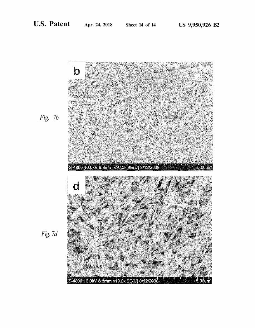
Fig. 7b
Fig. 7d

US 9,950,926 B2 1
METHOD FOR PRODUCTION OF GERMANIUM NANOWIRES
ENCAPSULATED WITHIN MULTI-WALLED CARBON NANOTUBES
This application claims the benefit of U.S. Provisional Patent Application Ser. No. 61/259,429 filed on 9 Nov. 2009, the entire disclosure of which is incorporated herein by reference.
2 catalyst was employed to catalyze the growth of the germa-nium nanowires which were then dispersed on an amor-phous carbon film and annealed. This resulted in the encap-sulation of the nanowires by well defined, curved graphene sheets. The presence of gold nanoparticles or residual cata-lysts on the surface of the nanowires is instrumental in initiating graphene sheet formation. Other methods which have been employed for the preparation of germanium/ carbon core sheet nanostructures include the arc discharge
TECHNICAL FIELD AND INDUSTRIAL APPLICABILITY OF THE INVENTION
10 synthesis of carbon nanotubes in the presence of germanium metal and the deposition of graphitic coatings on preformed germanium nanowires by their treatment with organic vapors at 700 and 900 degrees C.
The carbon arc discharge method, initially used for pro-The present invention relates generally to the field of nanotechnology and, more particularly, to a method of producing germanium nanowires encapsulated within multi-walled carbon nanotubes as well as to such nanowires as produced by that method.
15 ducing C60 fullerenes, is the most common and perhaps easiest way to produce multi-walled carbon nanotubes (MWCNTs ), as it is rather simple. This method creates MWCNTs through arc-vaporization of two carbon rods placed end to end, separated by approximately 1 mm, in an
BACKGROUND OF THE INVENTION 20 enclosure that is usually filled with inert gas at low pressure. A direct current of 50 to 100 A, driven by a potential difference of approximately 20 V, creates a high temperature discharge between the two electrodes. The discharge vapor-izes the surface of one of the carbon electrodes, and forms
Nanostructures such as nanotubes, nanowires and nano-belts are characterized by novel electronic and optical prop-erties intrinsically associated with their load dimensionality and the quantum confinement effect. Such nanostructures have potential applications in nanoelectronics, advanced composites, field emission devices, sensors, probes, optics and optoelectronics.
25 a small rod-shaped deposit on the other electrode. In order to produce MWCNTs filled with Ge (or indeed another element), a small cavity is bored out in the anode and packed with the desired element.
Silicon nanowires are of great technological importance in microelectronics. Silicon nanowires exhibit significant 30 differences in physical and chemical properties from bulk silicon. Compared to silicon, germanium nanostructures are
A disadvantage of the carbon arc discharge method is the fact that is produces a complex mixture of components which requires further purification, i.e., to separate the MWCNTs from the soot and the residual catalytic metals present in the crude product. Indeed, typical MWCNT yields do not exceed 50 weight percent, while single-walled carbon nanotube (SWCNT) yields can reach about 75 percent. This is also apparent for the Ge-filled MWCNTs reported by Dai et al. and by Loiseau et al. Low resolution TEM images of the Ge-filled MWCNTs obtained by Dai et al. clearly show the presence of signif icant amounts of spherical soot par-
of particular interest since the exciton Bohr radius of bulk germanium is larger than that of silicon. This results in more prominent quantum confinement effects. Germanium also 35 offers the advantage of lower processing temperatures with easier integration into conventional devices. Germanium also has much higher electron and hole mobility than silicon making germanium the preferred material for electronic devices scaled down to the Sub-100 nm regime.
Several growth methods are known in the art for the synthesis of germanium nanowires. These include laser ablation, thermal evaporation, super critical fluid synthesis, liquid-state synthesis, molecular beam epitaxy and chemical vapor deposition (CVD). CVD has been the most widely 45 employed of these synthesis methods to grow germanium nanowires from suitable catalysts and germanium precursors such as GeH4, Ge2H6, Ge(C5H5)2, C12H12Ge, Ge---Ge02 and Ge---GeI4. In most of the prior art CVD methods as well
40 ticles intimately mixed with the filled MWCNTs. Similarly, medium resolution TEM images reported by Loiseau et al. for MWCNTs filled with a variety of elements (including Ni, Sm, Dy, S, Sb, Pd, and Co) reveal the presence of amorphous
as the methods employing thermal evaporation of germa- 50 nium powders, gold nanoparticles have been typically selected as the catalyst for germanium nanowire growth via the vapor-liquid-solid (VLS) mechanism. This is due to the low utectic temperature of the G e - A u alloy. Other low melting point metals/alloys that have been employed as the 55 catalyst include Al, Cu, C u - N i and Fe(Ge).
Untreated germanium nanowires are reported to oxidize upon exposure to ambient conditions. Since germanium oxide coatings possess unfavorable electronic properties such nanowire oxidation degrades the performance of any 60 nanodevice incorporating germanium nanowires. Accord-ingly, it is necessary to protect any germanium nanowires from oxidation.
One way to control or limit germanium oxidation is by carbon-encapsulation of the carbon-germanium nanowires. 65 This has previously been done using a chemical vapor deposition (CVD) technique. Specifically, a supported gold
carbon particles mixed with the nanotubes. This presents a clear disadvantage for the production of Ge-filled MWCNTs for microelectronics applications since purification of the crude product would be required.
The present invention is a simple one or two step syn-thesis method using a combined germanium and carbon source. The nanowires resulting from the present invention are characterized by high thermal stability and high electri-cal conductivity. In contrast to the prior CVD methods, the current method is catalyst free while the reaction product is clean and pure, incorporating greater than 95 weight percent germanium nanowires encapsulated in MWCNTs and less than 5 weight percent amorphous material.
SUMMARY OF THE INVENTION
In accordance with the purposes of the present invention as described herein, a method is provided for the production of germanium nanowires encapsulated within multi-walled carbon nanotubes. The method may be broadly described as comprising the steps of performing chemical vapor deposi-tion using a combined germanium and carbon source having a general formula ofGeRc4-x)Lx (where x=O, 1, 2 or 3 and R is selected from a group consisting of alkyl, cycloalkyl or

US 9,950,926 B2 3
aryl and L=hydrogen, halide or alkoxide) and growing the germanium nanowires encapsulated within the multi-walled carbon nanotubes on a substrate. In a particularly useful embodiment, the combined germanium and carbon source has a general formula GeR4 where R is selected from alkyl, cycloalkyl or aryl. In yet another particularly useful embodi-ment, the combined germanium and carbon source is phe-ny ltrimethy !germane.
4 µm and an overall diameter of between about 50 and about 300 nm. The nanowire in the reaction product includes between about 95 and about 100 weight percent germanium and between about 5 and about O weight percent carbon. In one particularly useful embodiment the core includes between about 50 and about 99 weight percent germanium and between about 50 and about 1 weight percent iron.
In the following description there is shown and described several different embodiments of the invention, simply by The method may be a simple one step process using a
carrier gas selected from a group consisting of nitrogen, argon, helium, hydrogen and mixtures thereof. Alternatively, the method may include a two step process including first feeding said combined germanium and carbon source under an N2 carrier gas to form multi-walled carbon nanotube sheaths on channel walls of a template and then feeding said combined germanium and carbon source under a hydrogen and argon carrier gas mixture to fill the multi-walled carbon nanotube sheaths with germanium nanowires.
10 way of illustration of some of the modes best suited to carry out the invention. As it will be realized, the invention is capable of other different embodiments and its several details are capable of modification in various, obvious aspects all without departing from the invention. Accord-
15 ingly, the drawings and descriptions will be regarded as illustrative in nature and not as restrictive.
Alternatively, the method for the production of germa-nium nanowires encapsulated within multi-walled carbon 20 nanotubes may be described as comprising the steps of dissolving a combined germanium and carbon source in a liquid hydrocarbon solvent to form a feed solution, dispers-ing the feed solution into a stream of a carrier gas, intro-ducing the feed solution into a reactor through a reactor 25 inlet, volatilizing the feed solution in the reactor and grow-ing germanium nanowires encapsulated within multi-walled carbon nanotubes on a substrate in the reactor. The germa-nium and carbon source has a general formula of GeRc4-x)Lxas described above. 30
The method may further include the step of selecting the carrier gas from a group including nitrogen, argon, helium, hydrogen and mixtures thereof. The radical R in the general chemical formula of the combined germanium and carbon source may be selected from the group consisting of phenyl, 35 methyl, ethyl, n-propyl, isopropyl, n-butyl, tert-butyl, vinyl, ally! and cyclopentadienyl and mixtures thereof. In one particularly useful embodiment the combined germanium and carbon source is phenyltrimethylgermane. In yet another particularly useful embodiment the phenyltrimethylgermane 40 is mixed with ferrocene in the feed solution.
BRIEF DESCRIPTION OF THE DRAWINGS
The accompanying drawings incorporated herein and forming a part of the specification, illustrate several aspects of the present invention and together with the description serve to explain certain principles of the invention. In the drawings:
FIG. 1 is a cross sectional view of a nanowire incorpo-rating a germanium core surrounded by a multi-walled carbon nanotube sheath;
FIG. 2a is a scanning electron micrograph (SEM) image of Ge-filled MWCNTs synthesized at 800° C.;
FIG. 2b is a higher magnification SEM image showing MWCNTtips;
FIGS. 3a-3e are transmission electron micrograph (TEM) images of the Ge-filled MWCNT reaction product shown in FIGS. 2a and 2b;
FIGS. 4a and 4b are scanning/transmission electron micrograph (STEM) images of the Ge-filled MWCNT reac-tion product shown in FIGS. 2a-2b and 3a-3e;
FIG. 4c shows the results of energy dispersive x-ray spectroscopy (EDS) for the reaction product in FIG. 4b;
FIGS. Sa-Sc characterize the reaction product by respec-tively powder x-ray diffraction (XRD), x-ray photoelectron spectroscopy (XPS) spectrum and thermogravimetric analy-sis in air (10° C./min heating rate);
FIGS. 6a-6d are SEM images of reaction product using neat phenylmethylgermane starting material at, respectively 3, 4, 5 and 7 inches from the reactor inlet; and
The method includes providing the combined germanium and carbon source in the reactor at a concentration of between about 1,000 to about 10,000 ppm. In one useful embodiment the combined germanium and carbon source is 45 provided at a concentration of between about 1,850 to about 3,850 ppm. In another it is provided at a concentration of about 2,850 ppm. The method includes maintaining the reactor at a temperature of between about 800 and about 1,000 degrees C.
FIGS. 7a-7d are SEM images of the reaction product obtained using 50 weight percent phenylmethylgermane in xylene as the starting material at, respectively, 3, 4, 5 and 7
50 inches from the reactor inlet. The method also includes using a substrate made from a
material selected from a group consisting of quartz, anod-ized aluminum oxide, sapphire, aluminum coated quartz, aluminum coated silicon and mixtures thereof. The method may also include growing the encapsulated germanium 55 nanowires in an array by depositing germanium and carbon from the combined germanium and carbon source within the pores of a template.
In accordance with yet another aspect of the present invention, a reaction product from a process of growing 60 germanium nanowires is provided. The reaction product is characterized by comprising greater than 60, 70, 80, 90 and even 95 weight percent germanium nanowires encapsulated in multi-walled carbon nanotubes and, respectively, less than 40, 30, 20, 10, and even 5 weight percent amorphous 65 material in the absence of performing any purification step. The nanowire has a length of between about 6 and about 50
Reference will now be made in detail to the present preferred embodiment of the invention, examples of which are illustrated in the accompanying drawings.
DETAILED DESCRIPTION OF THE PREFERRED EMBODIMENTS OF THE
INVENTION
Reference is now made to FIG. 1 which is a cross sectional illustration of a nanowire 10 incorporating a ger-manium core 12 surrounded by a multi-walled carbon nano-tube (MWCNT) sheath 14 as produced in accordance with the method of the present invention. That method for the production of germanium nanowires encapsulated within MWCNTs may be broadly defined as comprising the steps of (1) performing chemical vapor deposition using a com-bined germanium and carbon source and (2) growing ger-

US 9,950,926 B2 5
manium nanowires encapsulated within multi-walled carbon nanotubes on a substrate. The germanium and carbon source has a general formula o f GeRc4-x)Lx, where x= O, 1, 2, or 3;
6 be mixed with a doping agent such as ferrocene including anywhere from between about 99 weight percent to about 50 weight percent phenyltrimethylgermane with the remainder ferrocene. In the case o f ( c ), a sufficient amount o f a hydrocarbon solvent such as pyridine, xylene, toluene or benzene is preferably added to ensure dissolution o f the ferrocene.
The reaction product resulting from the process o f the present invention for growing germanium nanowires encap-
R is selected from a group consisting o f alkyl, cycloalkyl or aryl and L = hydrogen, halide or alkoxide. In a particularly useful embodiment the combined germanium and carbon source has a general formula o f GeR4 where R is selected from a group consisting of alkyl, cycloalkyl or aryl. In yet another particularly useful embodiment o f the present inven-tion the combined germanium and carbon source comprises phenyltrimethylgermane. The phenyltrimethylgermane may be utilized neat or mixed with ferrocene.
The method o f the present invention for the production o f germanium nanowires encapsulated within MWCNTs may
10 sulated within multi-walled carbon nanotubes has a number o f distinct characteristics. Specifically, the reaction product obtained directly from the process is characterized by com-prising greater than 60 weight percent germanium nanowires encapsulated in multi-walled carbon nanotubes and less than
be more specifically defined as comprising the dissolving o f the combined germanium and carbon source in a liquid hydrocarbon solvent to form a feed solution, dispersing the feed solution into a stream o f carrier gas, introducing the feed solution in the carrier gas into a reactor through a reactor inlet, volatilizing the feed solution in the reactor and growing germanium nanowires encapsulated within MWCNTs on a substrate in the reactor. The liquid hydro-carbon solvent may be, for example, pyridine, benzene, toluene, xylene or any liquid hydrocarbon solvent appropri-
15 40 weight percent amorphous material. These purity num-bers are attained in the absence o f performing any purifica-tion step. In fact, the actual product may be characterized by comprising greater than 70, 80, 90 and even 95 weight percent germanium nanowires encapsulated in multi-walled
20 carbon nanotubes and less than, respectively, 30, 20, 10 and even 5 weight percent amorphous material in the absence o f performing any purification step. This pure, clean product is particularly advantageous for ultimate use in nanostructures including particularly those for nanoelectronic applications
25 relating to, but not limited to, advanced composites, field emission devices, sensors, probes, optics and optoelectron-
ate for dissolving the combined germanium and carbon source. The combined germanium and carbon source to solvent ratio should be between 1 :5 and 1 :0 and more preferably between 1:2 and 1:0. The carrier gas may be selected from a group including nitrogen, argon, helium, hydrogen and mixtures thereof. Mixtures o f from about 5 to 30 about 30 percent hydrogen and the remainder argon are particularly useful.
JCS.
The multi-walled carbon nanotubes that form the sheath 14 around the germanium core 12 have a thickness o f between about 5 and about 10 mm. The nanowire itself has a length o f between about 6 and about 50 µm and an overall diameter o f between about 50 and about 300 nm. Particu-larly useful embodiments o f nanowires prepared using the present method have a length o f between about 10 and about 50 µm and more preferably between about 20 and about 50 µm and an overall diameter o f between about 50 and about 300 nm. The nanowires also include between about 95 and about 100 weight percent germanium and between about 5 and about O weight percent carbon. Typically, the nanowires
As noted above, the germanium and carbon source has a general formula o f GeRc4-x)Lx where x= O, 1, 2 or 3; R is selected from a group consisting o f alkyl, cycloalkyl or aryl 35 and L = hydrogen, halide or alkoxide. In some particularly useful embodiments o f the invention, the radical R is selected from a group o f radicals consisting o f phenol, methyl, ethyl, vinyl, n-propyl, iso-propyl, ally!, n-butyl, tert-butyl, cyclopentadienyl and mixtures thereof.
The method further includes providing the combined germanium and carbon source in the reactor at a concentra-tion o f between about 1000 to about 10,000 ppm. In another particularly useful embodiment of the invention the method includes providing the combined carbon and germanium 45 carbon source in the reactor at a concentration o f between about 1,850 to about 3,850 ppm. In still another particularly useful embodiment o f the present invention the method includes providing the combined germanium and carbon source in the reactor at a concentration o f about 2,850 ppm. 50 In addition, the method includes maintaining the reactor at
40 include about 97 weight percent germanium and about 3 weight percent carbon. Where the combined germanium and carbon source is phenyltrimethylgermane mixed with ferro-cene, the core 12 includes between about 50 and about 99
a temperature o f between about 700 and about 1,000 degrees C . and more typically between about 800 and about 900 degrees C . during the production process.
The method further includes using a substrate made from 55 a material selected from a group consisting o f quartz, anodized aluminum oxide, sapphire, aluminum coated quartz, aluminum coated silicon and mixtures thereof. In one particularly useful embodiment the method includes grow-ing the encapsulated germanium nanowires in an array by 60 depositing germanium and carbon from the combined ger-manium and carbon source within pores in a template such as an anodized aluminum oxide template. Using phenylt-rimethylgermane as the combined germanium and carbon source is particularly beneficial when growing a germanium 65 nanowire array. The phenyltrimethylgermane may be used (a) neat, (b) mixed with a solvent such as xylene or (c) it may
weight percent germanium and between about 50 and about 1 weight percent iron. The following synthesis and examples are provided to further illustrate the invention, but it is not to be considered as limited thereto.
Example 1
Preparation o f Ge-Filled MWCNTs The two-zone furnace employed for the C V D preparation
consisted of a quartz tube reactor (with inner diameter o f 28 mm) and a flat quartz slide inserted at the reaction zone for additional deposition surface. Neat phenyltrimethylgermain (PTMG) was injected into the preheat zone o f the reactor at a rate o f 1 ml/h. After volatilization in the preheat zone (-250° C.), the PTMG was carried into the reaction zone o fthe furnace, maintained at 800° C. , by a 10% H i Ar sweep gas (750 cm3/min flow rate). The entire system was main-tained at a slight positive pressure (-0.75 kPa) versus atmospheric pressure. Typical C V D runs were o f 2 h dura-tion, after which the material deposited on the quartz slide was collected for analysis.
Characterizations Scanning electron microscopy (SEM) was performed
using a Hitachi S-2700 microscope equipped with a LaB 6

US 9,950,926 B2 7 8
electron gun, as well as a field emission Hitachi S-4800 high resolution microscope. Transmission electron microscopy (TEM), high-resolution TEM (HRTEM), scanning transmis-sion electron microscopy (STEM) and energy dispersive X-ray spectroscopy (EDS) were conducted using a JEOL 5 2010 field emission TEM operated at 200 kV. QuantitativeEDS analysis was perform under STEM mode by locatingthe analytical probe at the center position of the encapsu-lated Ge nanowires. EDS spectra were collected using anOxford Analytical detector. Spectra were background sub- 10 tracted and C/Ge peak fitting was performed using theEsVision microanalysis system. The error on the resultingGe and C concentrations is estimated at not more than+/-10%.
tion peaks (28=27.43, 45.45, 53.83, 66.13, 73.11, 83.79°) are in good agreement with literature values for the crystal-line face centered cubic phase of Ge with lattice parameter a=5.660 A. Furthermore, the neighbor interlayer spacing indexed in HRTEM images (see FIG. 3e) is approximately 3.29 A, which is very close to the calculated distance between neighboring (111) planes of 3.27 A. Thus the as-produced Ge@MWCNT/800 consists primarily of FCC Ge.
X-ray photoelectron spectroscopy (XPS) was used to study the oxidation state of the Ge in the nanowires. As shown in FIG. Sb, two Ge 3d photoelectron lines are observed. The signal corresponding to a binding energy of
Powder X-ray diffraction (XRD) measurements were per-formed on a Phillips X'Pert diffractomer using Cu Karadiation (A= l .5406 A) and a step size of 0.02 °. X-ray photoelectron spectroscopy (XPS) analyses were performed on a PHI 5600 LS instrunient, using a non-monochromatic Al source. The analysis area was 1 x3 mm. The C 1 s line (285.0 eV) was employed as a binding energy standard. Thermogravimetric analysis (TGA) was performed using a TA Instruments TGA Q500 system. Samples were heated in a flow of air (50 cm3/min) at 10° C./min from room temperature to 1000° C.
Representative scanning electron micrographs of the material prepared at 800° C. are shown in FIG. 2. These show the sample to consist mainly of nanowires, possessing diameters ofless than 500 nm (see FIG. 2b). The nanowires appear smooth, with little evidence of metal cluster forma-tion. Furthermore, from FIG. 2 and other micrographs, it is apparent that the as-synthesized nanowires are largely free from amorphous carbon and possess large aspect ratios, the typical length being in the order of 10 µm. In contrast, syntheses carried out at 700° C., 900° C. and 1000° C. did not yield Ge-containing nanowires. At 700° C. decomposi-tion of the precursor appears to be incomplete; consequently, only a few short wires are formed. Increase of the tempera-ture above 800° C. results in the formation of amorphous carbon, with Ge nanoparticle formation being favored over the formation of nanowires.
More detailed microstructural investigations were per-formed in TEM and STEM/EDS modes, the latter using a 1 nm analytical probe. As revealed by TEM, the product obtained at 800° C. (hereafter denoted as Ge@MWCNT/ 800) consists of crystalline Ge nanowires, encapsulated in athin MWCNT sheath. Typical TEM images at low magni-fication (see FIGS. 3a and 3b) reveal a pin-like morphology.TEM images at higher magnification (FIG. 3d, 3e) show thatthe Ge nanowires consist of well crystallized Ge cores whichare completely encapsulated by the sheath-like MWCNTs possessing a thickness of 5-10 nm. Ge incorporation withinthe graphene sheets of the MWCNTs is not observed accord-ing to EDS analysis under STEM mode. Quantitative EDS analysis of the tube cores (see FIG. 4) indicates a compo-sition of 95% Ge and 5% C (atom%). Given the existenceof 5-10 nm thick of graphene (C) layers covering the Ge core at the analytical probe position, we can reasonably concludethat the core consists of pure Ge, as supported by HRTEM observations that show clear fringes corresponding to single crystal Ge (see FIG. 3e). Furthermore, EDS analysis con-firmed that the near spherical heads of the nanowires consistof over 97 atom % Ge (the balance being C).
Powder XRD measurements were performed to identify crystalline phases in the as-synthesized samples. FIG. Sa shows the XRD pattern obtained from sample Ge@MWCNT/800. The positions of the observed diffrac-
15 29.7 eV can be assigned to Ge metal, albeit that it is slightly shifted (-0.3 eV) compared to typical 3d binding energies reported for bulk Get . This phenomenon has been observed previously and is attributed to the dimensional confinement of the Ge. The other signal at 32.5 eV is characteristic of
20 Ge02.t Deconvolution of the signals and integration indi-cates a Ge(O):Ge(IV) atomic ratio of 78:22, suggesting that the Ge nanowires are largely, although not completely, protected from oxidation. Additionally, it is likely that amorphous, partially oxidized Ge is present, which contrib-
25 utes to the Ge02 signal. While SEM analysis of Ge@MWCNT/800 suggests that nanowires constitute at least 80% of the sample, the presence of irregularly shaped Ge particles can be observed in some SEM images (as shown in FIG. 6c).
3o t NIST Standard Reference Database 20, Version 3.4 (Web Version), http:/ srdata.nist.gov/xps/.
The results of thermogravimetric analysis performed on Ge@MWCNT/800 in air are shown in FIG. Sc. Noteworthy is the observation that a pronounced increase in sample
35 weight commences at around 550° C., consistent with the oxidation of Ge to Ge02. This temperature corresponds to the initiation of MWCNT combustion, suggesting that Ge oxidation proceeds as the nanowires' outer carbon shells are
40 oxidized and the Ge cores are exposed. Allowing for the initial carbon content of3 wt.% in the sample (by elemental analysis), and assuming that all of the Ge present is oxidized to Ge02, the observed gain in sample weight (37%) corre-sponds to an initial molar Ge:Ge02 ratio of 86:14 (in
45 reasonable agreement with the value determined by XPS). In order to provide insight into the factors controlling
nanowire formation, CVD experiments were performed in which the deposited solid was sampled from quartz slides placed at fixed distances from the inlet, i.e., along the length
50 of the tube reactor. The reaction zone was again held at 800°
C. SEM images of these materials are shown in FIGS. 6 and7. Images 6a-6d correspond to a CVD run performed usingneat PTMG as the precursor, while images 7a-7d correspondto the product obtained using PTMG diluted to 50 wt% with
55 xylene. For both runs, light deposits of mainly amorphous Ge particles were obtained closest to the inlet. For the run using neat PTMG, nanowires could be found in a localized region of the reactor, between 4" and 5" from the inlet. Further away from the inlet, Ge particles were obtained
60 (FIG. 6d). Evidently, while carbon is available beginning at 4" from the inlet from cracking of the PTMG, the partial pressure of carbon in the atmosphere is insufficient to produce Ge-filled nanotubes along the entire length of the reactor. In contrast, when the PTMG/xylene mixture was
65 used, not only was the total yield of Ge-filled nanotubes increased (estimated at >50% based on Ge), Ge-filled nano-tubes were observed in the entire region 4"-7" from the inlet.

US 9,950,926 B2 9
Furthermore, the dimensions of the filled nanotubes were rather uniform, with diameters in the 200-300 nm range and lengths of 6-10 µm.
For the runs performed with both neat PTMG and PTMG/ xylene, structures could be observed which appear to cor-respond to the early stages of nanotube/nanowire growth. Examples of this are shown in the circled regions of FIG. 6b. CNT growth evidently occurs from the Ge particle and appears to carry Ge as a nanowire away from the initial particle. Presumably, this synthesis mode is the result of 10 wetting at the interface of the Ge and the growing carbon nanotube. This is illustrated in FIG. 3c, 3d, which shows the high degree of association between the carbon sheath and the Ge nanowire. It should be noted that the synthesis temperature used (800° C.) was more than 100° C. lower 15 than the melting point of Ge (938° C.). Differential scanning calorimetry (DSC) performed under N2 indicates a m.p. of 934° C. for the Ge nanowires. While this is only slightly lower than the melting point for bulk Ge, it has been reported that smaller nanoscale metal structures can exhibit much 20
10 practical application to thereby enable one of ordinary skill in the art to utilize the invention in various embodiments and with various modifications as are suited to the particular use contemplated. All such modifications and variations are within the scope of the invention as determined by the appended claims when interpreted in accordance with the breadth to which they are fairly, legally and equitably entitled. The drawings and preferred embodiments do not and are not intended to limit the ordinary meaning of the claims in their fair and broad interpretation in any way.
What is claimed: 1. A reaction product resulting from a process of growing
germanium nanowires encapsulated within multi-walled carbon nanotubes;
said reaction product being characterized by comprising greater than 60 weight percent germanium nanowires encapsulated in multi-walled carbon nanotubes and less than 40 weight percent amorphous material in the absence of performing any purification step, wherein said multi-walled carbon nanotubes form a sheath having a thickness of about 5 to about 10 nm. greater melting point depression. Hence, melting point
depression can be expected during the initial stages of nanowire growth. This effect, together with possible capil-lary action, can explain the apparently low Ge viscosity and the tendency for CNT filling by Ge.
This approach represents a simple method for the prepa-ration of carbon-encapsulated Ge nanowires. The nanowires can be tailored to dimensions of200-300 nm in diameter and 6-10 µm in length by selecting as CVD parameters a feed of 50 wt% PTMG in xylene and a process temperature of 800°
C. These results may offer new possibilities for the appli-cation of Ge nanowires in micro-electronic devices.
2. The reaction product of claim 1, wherein said reactionproduct is characterized by comprising greater than 70 weight percent germanium nanowires encapsulated in multi-
25 walled carbon nanotubes and less than 30 weight percent amorphous material in the absence of performing any puri-fication step.
3. The reaction product of claim 1, wherein said reactionproduct is characterized by comprising greater than 80
30 weight percent germanium nanowires encapsulated in multi-walled carbon nanotubes and less than 20 weight percent amorphous material in the absence of performing any puri-fication step.
Example 2 4. The reaction product of claim 1, wherein said reaction35 product is characterized by comprising greater than 90
weight percent germanium nanowires encapsulated in multi-walled carbon nanotubes and less than 10 weight percent amorphous material in the absence of performing any puri-
Using the apparatus described above, with AAO as the substrate, PTMG is fed to the CVD reactor at a rate of 1 ml/h, using N2 as the carrier gas (at a flow rate of 750 cm3/min) and a reactor temperature of 800-900 degrees C. These conditions are maintained for between 5 and 30 min, 40 providing sufficient time for MWCNT sheaths to form on the channel walls of the AAO. After this period has elapsed, the carrier gas is switched to 10% H2/Ar (750 cm3/min flow rate), while maintaining a PTMG injection rate of 1 ml/h. This results in the formation of Ge-nanowires in the pre-formed MWCNT sheaths. Typically PTMG injection into the H2/Ar carrier gas is maintained for at least 2 hours, resulting in the formation of long (50 µm) encapsulated nanowJres.
fication step. 5. The reaction product of claim 1, wherein said reaction
product is characterized by comprising greater than 95 weight percent germanium nanowires encapsulated in multi-walled carbon nanotubes and less than 5 weight percent amorphous material in the absence of performing any puri-
45 fication step. 6. The reaction product of claim 1 wherein said nanowire
has a length of between about 6 and about 50 µm and an overall diameter of between about 200 and about 300 nm.
The foregoing description of the preferred embodiments 7. The reaction product of claim 1 wherein said nanowire
50 has a length of between about 10 and about 50 µm and an overall diameter of between about 200 and about 300 nm. of the present invention have been presented for purposes of
illustration and description. It is not intended to be exhaus-tive or to limit the invention to the precise form disclosed. Obvious modifications or variations are possible in light of the above teachings. Dopants other than iron may be used. 55 Thus, one could mix the phenyltrimethylgermane (PTMG) with precursors of other metals or metalloid elements so as to introduce a range of metal dopants into the germanium. The metal dopant precursor used should be miscible with or soluble in the PTMG or PTMG solution. The metal dopant 60 should undergo thermal decomposition at a temperature above the temperature at which the injection is performed (ca. 250 deg. C.) and below the reactor temperature (700-1,000 deg. C.). Further, the dopant should form a solid solution with germanium in the nanowires. 65
The embodiments were chosen and described to provide the best illustration of the principles of the invention and its
8. The reaction product of claim 1 wherein said nanowirehas a length of between about 20 and about 50 µm and an overall diameter of between about 200 and about 300 nm.
9. The reaction product of claim 8 wherein said nanowireincludes between about 95 and about 100 weight percent germanium and between about 5 and about O weight percent carbon.
10. The nanowire of claim 1 wherein said core includesbetween about 50 and about 99 weight percent germanium and between about 50 and about 1 weight percent iron.
11. A reaction product resulting from the process of: performing chemical vapor deposition using a combined
germanium and carbon source having a general formula ofGeRc4-x)Lx, where x=O, 1, 2, or 3; R is selected from a group consisting of alkyl, cycloalkyl or aryl and L=hydrogen, halide or alkoxide; and

US 9,950,926 B2 11
growing germanium nanowires encapsulated within multi-walled carbon nanotubes;
said reaction product being characterized by comprising greater than 60 weight percent germanium nanowires encapsulated in multi-walled carbon nanotubes and less than 40 weight percent amorphous material in the absence of performing any purification step wherein said reaction product has a germanium to carbon ratio of 5: 1.
12. The reaction product of claim 1, wherein said reaction 10 product has a germanium to carbon ratio of 9: 1.
* * * * *
12